BIOTRONIK SE and KG CM06-1 Patient Device User Manual
BIOTRONIK SE & Co. KG Patient Device
Contents
- 1. Manual1
- 2. Manual2
- 3. Manual3
- 4. user manual
user manual

Applicant: Motorola Inc. FCC ID:IHDT56FV1
Exhibit 8
Page 1 of 8
G24 Developer Guide
Table of Contents
GENERAL.........................................................................................................................2
GENERAL DESCRIPTION............................................................................................ 3
GETTING STARTED...................................................................................................... 5
GENERAL PURPOSE SWITCHES............................................................................... 6
EMU
B
US
–
UID
PIN
........................................................................................................ 6
A/D
OPERATION
............................................................................................................... 6
GPIO ............................................................................................................................... 7
A
UDIO
.............................................................................................................................. 7
SPI................................................................................................................................... 7
G
ENERAL
P
OSITIONS
........................................................................................................ 8

Applicant: Motorola Inc. FCC ID:IHDT56FV1
Exhibit 8
Page 2 of 8
General
This document content describes the operation of the G24 Evaluation board (EVB) P1.
The G24 EVB supports two G24 versions: OEM, and fixed mobile. For the fixed mobile
a secondary board is mounted on EVB (“Piggy Board”, using connector P50).
The follow PDF file contains EVB schematic and layout (all References are searchable)
8899_schem_place_
s
earch.pdf
Applicant: Motorola Inc. FCC ID:IHDT56FV1
Exhibit 8
Page 3 of 8
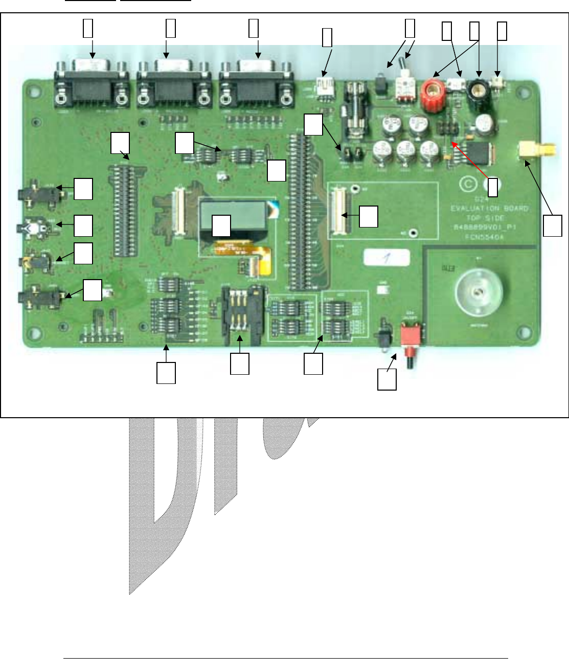
General Description
1) P210 - Battery socket connector for a Lithium-ion battery. Note: set P203 jumper to
battery, line 9.
2) J200, J201 – Lab Power Supply jacks. Note: set P203 jumper to P.S, line 9.
3) J230 – Wall Adapter connector. Note: set P203 jumper to adapter, line 9.
4) S200, D200 – Main power switch, and led indicator.
5) J380- EMU (Mini-USB) socket.
6) J300 – RS232-1, G24 UART 1.
7) J330 – RS232-2, G24 UART 2.
8) J350 – RS232-SPI, G24 SPI bus debugger (enabled with line 14).
9) P203 – Selecting power supply Source. Connect jumper to select 1 of 3 options (Wall
Adapter, lab power supply, or battery). Note: G24 EVB shall not work if not
connecting this jumper.
10) P2 – G24EVB on board Antenna.
11) S110, D701 – G24 On/Off Switch and led indicator.
12) S160, S161, S171, S170 – General switches for testing.
10
22
G24 EVB – Top View (Without 2
nd
Keypad board)
8
11
7 654 3 2 1
9
19
21
18
17
16
15
13 12
10
20
14
23
24
22

Applicant: Motorola Inc. FCC ID:IHDT56FV1
Exhibit 8
Page 4 of 8
13) J100 – SIM Card socket.
14) S140, S120, S121 - General switches for testing.
15) J430 – Speaker Jack connector.
16) J460 – Microphone Jack connector.
17) J440 – Headset Jack connector.
18) J480 – Alert speaker Jack connector.
19) P50- 40 pin header for 2
nd
Keypad board (“Piggy Board”).
20) S100, S141 - General switches for testing.
21) P100 – 70-pin header. This header spreads G24 70 pin connector (P1) for signal
measuring.
22) CLI Display.
23) P1 – 70-pin connector for G24.
24) P201, P200 – Secondary power jumpers. G24EVB main power is divided to 2 roots,
1
st
to EVB, and 2
nd
to G24 unit.

Applicant: Motorola Inc. FCC ID:IHDT56FV1
Exhibit 8
Page 5 of 8
Getting Started
- Select power supply source (Wall Adapter, lab power supply, or battery), and connect
it to suitable jack (either line 1, 2, or 3).
- Set P203 jumper (line 9) according to your main power source selection.
- Make sure that P201, P200 jumpers are connected (line 24).
- Mount G24 on G24EVB using P1 connector (line 23).
- Connect G24 Antenna to P2 (line 10) - Optional
- Turn On main power switch S200 (line 4), led indicator D200 is On.
- Press S110 On/Off switch (line 11) for turning On G24 unit.
Applicant: Motorola Inc. FCC ID:IHDT56FV1
Exhibit 8
Page 6 of 8
General Purpose Switches
The G24 contains General Purpose Switches for simulating testing states. For detail
schematics see PDF file in General Section (at the beginning of this doc).
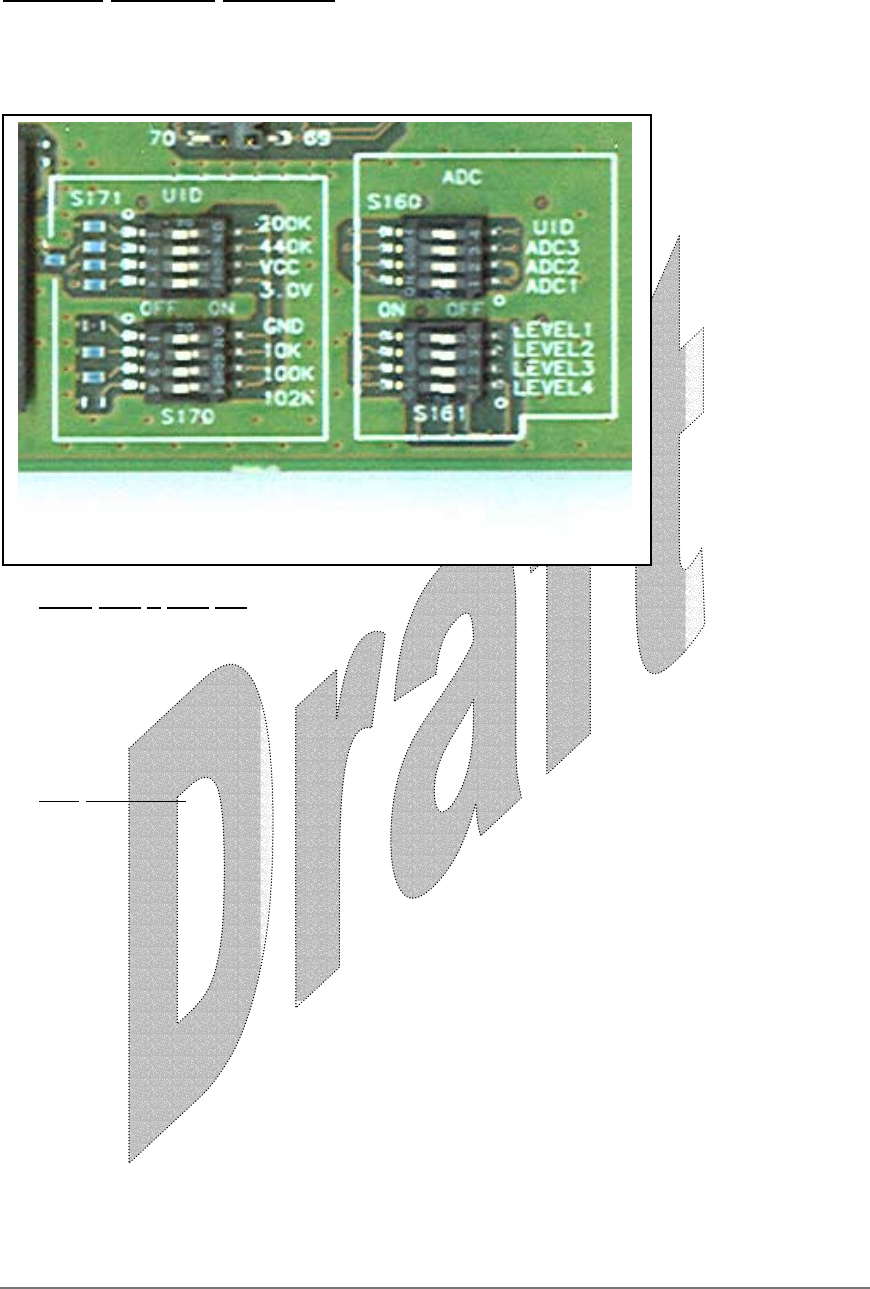
EMU Bus – UID pin
S170, S171 and S160 1
st
switch are used to simulate UID pin of the G24 EMU bus.
The default position (as shown in figure) is that UID pin is not connected.
- Switching On (left) S160 UID position shall enable S170, S171.
- Select Only one position from S170, S171 according to EMU spec.
A/D operation
G24 has 3 General A/D. G24 can simulate analog voltages vary from 0.1V-1.7V.
- Set S161 switch position to desired voltage level.
- Enable desired ADC (S160).
Line 12
Applicant: Motorola Inc. FCC ID:IHDT56FV1
Exhibit 8
Page 7 of 8
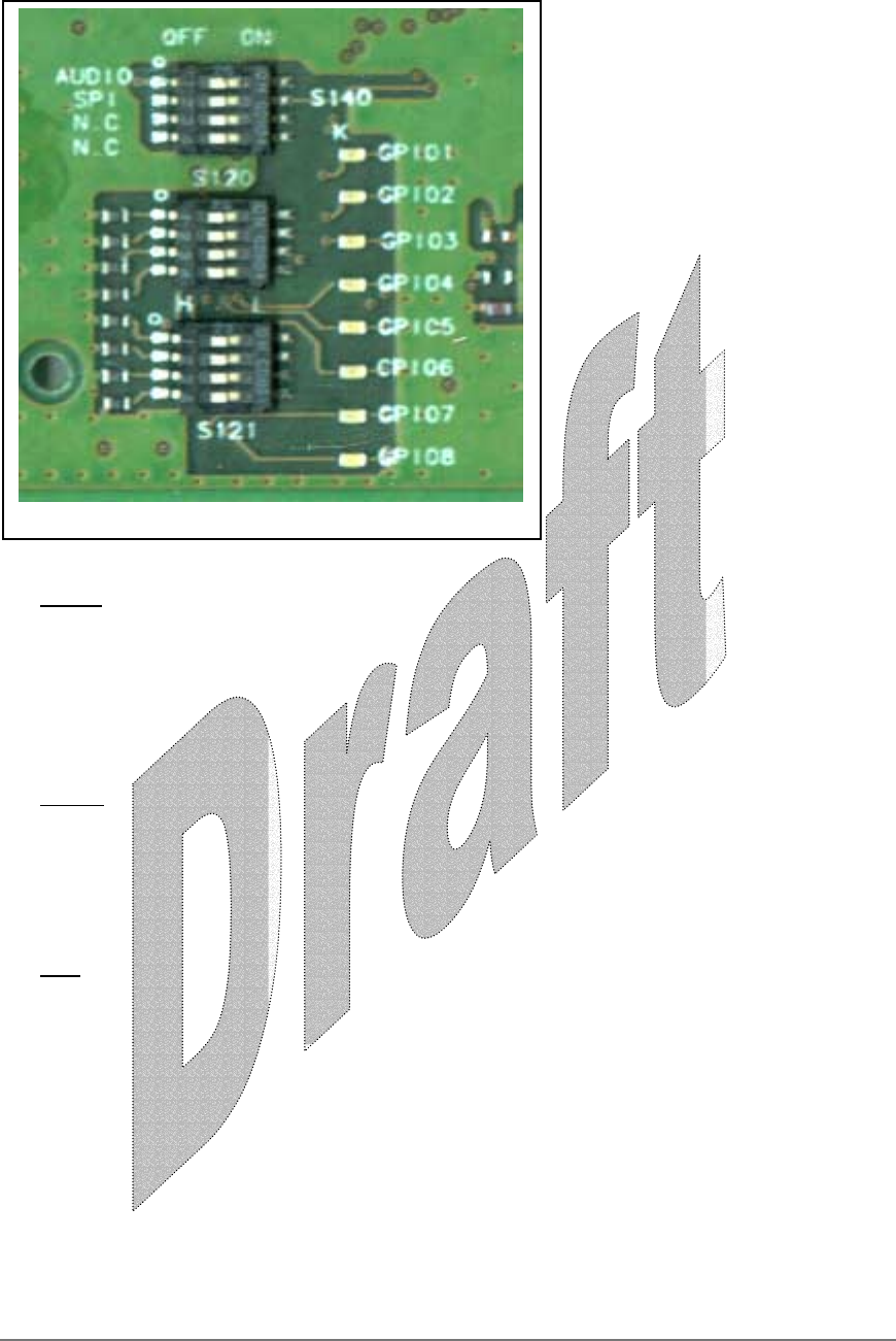
GPIO
G24 has 8 General Purpose I/O. S120, S121 along with GPIO led indicators simulate
GPIO state. G24 has internal pull-ups.
- Switch left position – GPIO line is disconnected.
- Switch right position – GPIO line is shorted to ground.
Audio
S140 Audio position selects the Audio path of G24.
- Switch left position – Analog Audio path (Using G24 internal vocoder).
- Switch right position – digital Audio path (Using G24EVB on board vocoder).
SPI
Enable SPI logger (line 8)
Line 14
Applicant: Motorola Inc. FCC ID:IHDT56FV1
Exhibit 8
Page 8 of 8
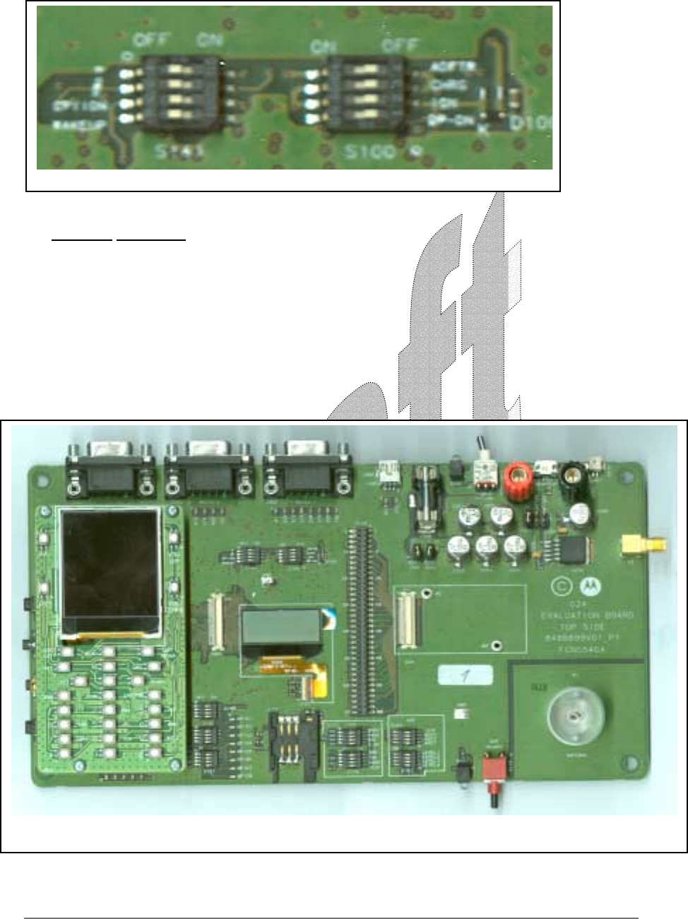
General Positions
- *, # - Simulating *, and # phone keys.
- Option – connects between WKUPO_N & WKUPI_N (Pins 16 & 26) in G24 70 pin.
- WAKEUP - connects WKUPI_N (pin 16) to ground
- ADPTR – connects Wall Adapter voltage to USB VBUS.
- CHRG – connects between USB VBUS to G24 Ignition.
- IGN – connect G24 Ignition to G24EVB voltage.
- DP-DN – connect between G24 USB DP & USB DN signals
Line 20
G24 EVB – Top View (With Keypad board)