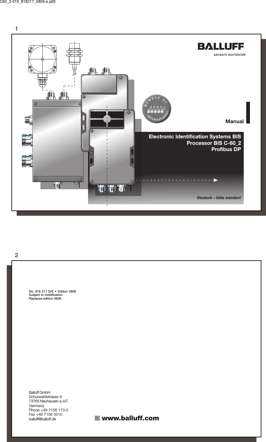
Balluff BISC6XX BIS C-6XX Module User Manual C60 2 019 818217 0806 e p65

Balluff Inc BIS C-6XX Module C60 2 019 818217 0806 e p65

Contents

User manual

1 Electronic Identification Systems BIS Processor BIS C-60_2Profibus DPManualDeutsch – bitte wenden!C60_2-019_818217_0806-e.p652No. 818 217 D/E •  Edition 0806Subject to modification.Replaces edition 0608.Balluff GmbHSchurwaldstrasse 973765 Neuhausen a.d.F.GermanyPhone +49 7158 173-0Fax +49 7158 5010balluff@balluff.de www.balluff.com
33englishContentsSafety Considerations................................................................................................................. 4Introduction, BIS C Identification Systems..............................................................................5-7BIS C-60_2 Processor, Basic knowledge for application ........................................................ 8/9BUS interface PROFIBUS-DP..............................................................................................10-12Compatibility with BIS C-6_2 processor .................................................................................. 13Function Description: Communication with the processor ................................................. 14Input and Output Buffers ............................................................ 15/16Output Buffer, configuration and explanation .............................17-20Input Buffer, configuration and explanation ................................ 21-24Parametering the BIS C-60_2 processor................................... 25-28Processing data carriers ............................................................ 29-35Examples for protocol sequence .............................................. 36-53Read/Write Times ............................................................................................................... 54/55LED Display ............................................................................................................................. 56BIS C-6002 BIS C-6022Mounting Head / Processor ..............................................................................57 .................. 75Opening the Processor .....................................................................................58 .................. 76Installing the connection cables / Mounting the PG connection .............. 59/60Interface information / Wiring Diagrams ..................................................... 61-68 ............. 77-80Changing the EEPROM .....................................................................................69 .................. 81Technical Data ............................................................................................. 70-72 ............. 82/83Ordering Information: Ordering Code / Accessory .................................... 73/74 .................. 84Appendix, ASCII Table ............................................................................................................. 85C60_2-019_818217_0806-e.p654english4Safety ConsiderationsSeries BIS C-60_2 processors along with the other BIS C system components comprise anidentification system and may only be used for this purpose in an industrial environment inconformity with Class A of the EMC Law.Installation and operation should be carried out by trained personnel only. Unauthorized workand improper use will void the warranty and liability.When installing the processor, follow the chapters containing the wiring diagrams closely.Special care is required when connecting the processor to external controllers, in particularwith respect to selection and polarity of the signals and power supply.Only approved power supplies may be used for powering the processor. See chapter 'Techni-cal Data' for details.Prevailing safety regulations must be adhered to when using the identification system. In par-ticular, steps must be taken to ensure that a failure of or defect in the identification systemdoes not result in hazards to persons or equipment.This includes maintaining the specified ambient conditions and regular testing for functionalityof the identification system including all its associated components.Should there ever be indications that the identification system is not working properly, itshould be taken out of commission and secured from unauthorized use.This manual applies to processors in the series BIS C-6002-019-...-03-... andBIS C-6022-019-050-03-....Installation andOperationUse and CheckingFault ConditionsScopeApproved Operation
55englishPrinciplesIntroductionBIS C Identification SystemsApplications☞This manual is designed to assist the user in setting up the control program and installing andstarting up the components of the BIS C Identification System, and to assure rapid, trouble-free operation.The BIS C Identification Systems belongs in the category ofnon-contact systems for reading and writing.This dual function permits applications for not only transporting information in fixed-program-med Data carriers, but also for gathering and passing along up-to-date information as well.If 2 read/write heads are connected to a BIS C-60_2 processor, both heads can be operatedindependently of each other. This means for example that you can read a Data carrier from onehead while writing to another Data carrier at the other head.Some of the notable areas of application include– for controlling material flow in production processes(e.g. in model-specific processes),for workpiece conveying in transfer lines,in data gathering for quality assurance,for gathering safety-related data,– in tool coding and monitoring;– in equipment organization;– in storage systems for monitoring inventory movement;– in transporting and conveying systems;– in waste management for quantity-based fee assessment.C60_2-019_818217_0806-e.p656english6BIS C-3_ _BIS C-35_ BIS C-3_ _BIS C-65_BIS C-670 BIS C-650System Components The main components of the BIS C Identification Systems are:–Processor,–Read/Write Heads and–Data carriersIntroductionBIS C Identification SystemsPROFIBUS-DPData carriers BIS C-1_ _-...Schematicrepresentation of anIdentification System(example)Processor  BIS C-6002withadapterRead/writeheads 1)1) BIS C-3_ _ series, except BIS C-350 and -352 2) only BIS C-350 or -352Read/writehead 2)Processor  BIS C-6002withadapterProcessor  BIS C-6002withread/write headConfiguration withBIS C-6002processor
77englishBIS C-3_ _BIS C-3_ _ BIS C-3_ _BIS C-3_ _IntroductionBIS C Identification SystemsRead/write heads1)Schematicrepresentation of anidentification system(example) 1) BIS C-3_ _ series, except BIS C-350 and -352PROFIBUS-DPData carriers BIS C-1_ _-...Configuration withBIS C-6022processorProcessor BIS C-6022version -050Processor BIS C-6022version -050C60_2-019_818217_0806-e.p658english8Selecting SystemComponentsThe BIS C-6002 processor has a plastic housing. Depending on the version, connections aremade either through a terminal strip, with the cable secured using a PG fitting, or via roundconnectors. A single read/write head from BIS C-65_ series can be directly mounted to theprocessor, which creates a compact unit. If the BIS C-650 adapter is attached instead of theBIS C-65_ read/write head, two read/write heads may be cable connected. If the BIS C-670adapter is attached, one read/write head may be cable connected.The BIS C-6022 processor has a metal housing. Connection is made through round connec-tors. Two read/write heads can be cable connected to the BIS C-6022 processor.Series BIS C-60_2 processors have in addition a digital input. The input has various functionsdepending on the configuration (see Parametering).Whether the compact version of the processor with integrated read/write head makes senseor whether the external solution is preferred depends primarily on the spatial arrangement ofthe components. There are no functional limitations. All read/write heads are suitable for bothstatic and dynamic reading. Distance and relative velocity are based on which Data carrier isselected. Additional information on the read/write heads in series BIS C-65_ and seriesBIS C-3_ _ including all the possible Data carrier/read-write head combinations can be foundin the manuals for the respective read/write heads.The system components are electrically supplied by the processor. The Data carrier repre-sents an free-standing unit and needs no line-carried power. It receives its energy from theread/write head. The latter constantly sends out a carrier signal which supplies the code headas soon as the required distance between the two is reached. The read/write operation takesplace during this phase. Reading and writing may be dynamic or static.BIS C-60_2 ProcessorBasic knowledge for application
99englishBIS C-60_2 ProcessorBasic knowledge for applicationThe processor writes data from the host system to the Data carrier or reads data from thetag through the read/write head and prepares it for the host system. Host systems mayinclude:–a host computer (e.g. industrial PC) or–a programmable logic controller (PLC)When sending data between the read/write head and the Data carrier a procedure is re-quired for recognizing whether the data were correctly read or written.The processor is supplied with standard Balluff procedure of double reading and compar-ing. In addition to this procedure a second alternative is available: CRC_16 data checking.Here a test code is written to the Data carrier, allowing data to be checked for validity atany time or location.Advantages of CRC_16   Advantages of double readingData checking even during the non-active phase(CT outside read/write head zone).No bytes on the data carrier need to bereserved for storing a check code.Shorter read times since each page is read onlyonce.Shorter write times since no CRC needs to bewritten.Since both variations have their advantages depending on the application, the user is freeto select which method of data checking he wishes to use (see Parametering on   26).It is not permitted to operate the system using both check procedures!Control FunctionData checking☞C60_2-019_818217_0806-e.p6510english10Communication between the BIS C-60_2 processor and the host system is via PROFIBUS-DP.The PROFIBUS-DP system consists of the components:– the bus master and– the bus modules/slaves (here the BIS C-60_2 processor).Important hints for use with PLC:In some control systems the PROFIBUS-DP data area is not synchronously transmitted with theupdating of the input/output content. If more than 2 bytes of data are sent, a mechanism mustbe used which guarantees that the data in the PLC and the data in the BIS C are always identi-cal!1st alternative: Synchronous data transmission as a setting on the MasterIn this method the bus Master ensures that all the data necessary for the respective Slave arealways sent contiguously. There is usually a special software function in the PLC which likewisecontrols access between the PLC and bus Master so that data are always sent contiguously.2nd alternative: Set 2nd bit headerData exchange between PLC and BIS is controlled by the so-called bit header. This is alwaysthe first byte of the respective read/write head in the data buffer. This bit header exists both inthe input range (data from BIS to the PLC) and in the output range (data from the PLC to theBIS). lIf this bit header is also sent as the last byte, a comparison of these two bytes can beused to guarantee the consistency of the transmitted data.In this method the PLC cycle is unaffected nor is the bus access time changed. All that isrequired is that a byte in the data buffer be used for the 2nd bit header instead of for user data.This 2nd alternative is the Balluff recommended setting (factory default).PROFIBUS-DP☞BUS interface PROFIBUS-DP
1111englishStation AddressFor the correct parametering of the bus master as per type, a diskette, containing the unit’smaster data in the form of a GSD file is included with the BIS C-60_2 processor.The Processor BIS C-60_2 is delivered with the station address 126. This has to be set indi-vidually before using in a bus system. See information on   12.An input buffer and an output buffer are used for the data exchange with the control system.The size of these buffers has to be configured via the master.The possible settings are entered in the GSD file (and Type file). A minimum of 4 and a maxi-mum of 128 bytes can be accommodated. However, it must be an even number.Besides, in the case of the BIS C-60_2 processor, there are 6 further bytes (User-ParameterBytes) which have to be set while parametering. The significance of the 6 bytes for para-metering is described starting from   25.The preset is stored in the GSD file.Input/Output BufferUnit's Master DataParametering BytesUser-Parameter Bytes☞☞BUS interface PROFIBUS-DPC60_2-019_818217_0806-e.p6512english12Station AddresssettingThe station address under which the unit is accessed on the bus can be assigned through theslide switch S1. Each address shall be assigned only once.The slide switch S1 is binary coded. The setting of the station address is carried out accordingto the scheme shown in the table. Switch position: no = left, yes = right.The address 85 is set in the following figure.➪no  yesTo open the cover of the processor, see   58 for BIS C-6002 or   76 for BIS C-6022.BUS interface PROFIBUS-DPSlide switch S1(with cover removed)StationAddressSlide switch S17654321262524232221200not allowed1 nonononononoyes2 nononononoyesno3 nononononoyesyes4 nonononoyesnono5 nonononoyesnoyes...85 yes no yes no yes no yes...123 yes yes yes yes no yes yes124 yes yes yes yes yes no no125 yes yes yes yes yes no yes126 yes yes yes yes yes yes no127 not allowed
1313englishSetting compatibility Slide switch S1 is used to set compatibility with the BIS C-602 and BIS C-622 processors.If the BIS C-60_2 processor is set to be compatible with the BIS C-602 or BIS C-622, all set-tings for data exchange must be made as described in the sections on parametering, functiondescription, protocol sequence and LED display in the user’s manual for the BIS C-6_2 proces-sor! This user’s manual can be mailed on request, or you may download it from the Internet atwww.balluff.de.Slide switch S1(with cover removed)➪no  yesKey: no = switch leftyes = switch rightIn the illustration compatibility with the BIS C-6_2 is not set.To open the cover of the BIS C-6002 processor, see   58,and for BIS C-6022 see   76.Slide switch S18 compatible withyes BIS C-6_2no BIS C-60_2☞Compatibility with BIS C-6_2 processorC60_2-019_818217_0806-e.p6514english14Function DescriptionCommunication with the processorCommunication between the host system and the processor takes place using a fixed proto-col sequence. Data integrity from the control to the processor and vice-versa is indicated by acontrol bit. This bit is used to implement a handshake between the control and the processor.Following is a simplified representation of the sequence of a job sent from the control to theprocessor:1. The control sends a command designator to the processor together with the associatedcommand parameters and sets a bit (AV bit). This bit indicates to the processor that thetransmitted data are valid and that the job is now beginning.2. The processor takes the job and sets a bit (AA bit), which indicates this to the control.3.  If an additional exchange of data between the control and the processor is required tocarry out the job, each uses a bit (TI bit and TO bit) to indicate that the control / processoris now ready for additional data exchange or has accepted the received data.4. Once the processor has carried out the job correctly, it sets a bit (AE bit).5. Once the control has accepted all the important data, it indicates this to the processor byresetting the bit that was set at the beginning (AV bit).6. The processor now in turn sets all the control bits that were set during the sequence(AA bit, AE bit) and is ready for the next job.Please see also 29...35 and theexamples on 36...53.Basic Procedure
1515englishInput and OutputBuffersIn order to transmit commands and data between the BIS C-60_2 and the host system, thelatter must prepare two fields. These two fields are:–the output bufferfor the control commands which are sent to the BIS Identification System andfor the data to be written.–the input bufferfor the data to be read andfor the designators and error codes which come from the BIS Identification System.The possible setting values are stored in the GSD file.The buffer size can be selected between 4 and 128 bytes in steps of 2 bytes. This must begiven by the master during parametering. The total buffer size is divided into 2 ranges:Buffer range 1 for Read/Write Head 1; size is specified in paramter byte 6.Buffer range 2 for Read/Write Head 2; size = total buffer size – buffer size of Read/WriteHead 1. See   16 for example.If a buffer size of less than 6 bytes (8 bytes with double bit header) is set for a read/write head, aread/write request can be carried out without specifying the start address and the number ofbytes. Automatic reading for Codetag-Present (see   30) remains active. This permits fastreading of small data quantities without placing an unnecessary load on the bus.Buffer size – 1 = number of bytes read without double bit header;Buffer size – 2 = number of bytes read with double bit header.☞Function DescriptionInput and Output BuffersPlease note thebasic procedure on 14 and 29...35and the examples onpages   36...53.C60_2-019_818217_0806-e.p6516english16Function DescriptionInput and Output Buffers☞Example: The 82 bytes for the total buffer need to be distributed. An input/output buffer of46 bytes is assigned to Read/Write Head 1. This results in an input/output buffer of 36 bytesfor Read/Write Head 2.Procedure: The buffer size for Read/Write Head 1 is set to 46 bytes. This means using theparameter byte 6 to enter Hex value 2E (corresponds to 46 decimal), which corresponds tobinary 00101110.PLC Organisation: The buffer range starts at input byte IB 32 and output byte OB 32.Result:Read/Write Head 1: Subaddress 00 IB 32 and OB 32(R/W 1) Input buffer IB 32 to IB 77Output buffer OB 32 to OB 77Read/Write Head 2: Subaddress 00 IB 78 and OB 78(R/W 2) Input buffer IB 78 to IB 113Output buffer OB 78 to OB 113IB 0 / OB 0 PLC bufferBuffer for R/W 1Buffer for R/W 2Input and OutputBuffers(continued)Note that these buffers can be in two differentsequences depending on the type of control.The following description is based on sequence 1!Sequence 1 Sequence 2Subaddress 00 Subaddress 0101 0002 0303 0204 0505 0406 0707 06Please note thebasic procedure on 14 and 29...35and the examples onpages   36...53.
1717englishThe last byte can be arranged as a 2nd bit header through parametering (default).Function DescriptionOutput buffer, configuration and explanationBit No.765432 10Subaddress00Hex = Bit Header CT TI HD GR AV Bit Name01Hex Command Designator or Data02Hex Start Address (Low Byte) or Program No.  or Data03Hex Start Address (High Byte) or Data04Hex No. of Bytes (Low Byte) or Data05Hex No. of Bytes (High Byte) or Data06Hex Data... DataLast Byte 2nd Bit Header (as above) or DataSub- Bit Meaning Function Descriptionaddress Name00Hex CT Data carrier type Select Data carrier type: for Data carrier type:Bit Header 0 32 Byte block size BIS C-1_ _-02, -03, -04, -051 64 Byte block size BIS C-1_ _-10, -11, -30TI Toggle-Bit In Shows during a read action that the controller is readyfor additional data.HD Head select for Head 1 for Head 20 Select Head 1.1 Select Head 2.11 Select Head 1.2 Select Head 2.2(only in conjunction with Adapter 655)(continued next  )Configuration of theoutput buffer for one(1) read/write headDescription ofOutput BufferPlease note thebasic procedure on 14 and 29...35and the examples onpages   36...53.C60_2-019_818217_0806-e.p6518english18Function DescriptionOutput buffer, configuration and explanationSub- Bit Meaning Function Descriptionaddress Name00Hex GR Ground state Causes the BIS system to go to the ground stateBit Header for the respective read/write head.Any pending command is cancelled.AV Command Signals the identification system that a commandfor the respective read/write head is present.Sub- Meaning Function Descriptionaddress01Hex Command designator00Hex No command present01Hex Read Data carrier02Hex Write to Data carrier06HEX Store program in the EEPROM for the Mixed Data Accessfunction07HEX Store the start address for the Auto-Read function in theEEPROM11HEX Copying from Head 1 to Head 212HEX Initialize the CRC_16 data check21HEX Read for Mixed Data Access function(corresponding to the program stored in the EEPROM)22HEX Write for Mixed Data Access function(corresponding to the program stored in the EEPROM)or Data for writing to the Data carrieror Program data for writing to the EEPROM.(continued next  )Description ofOutput Buffer(continued)Please note thebasic procedure on 14 and 29...35and the examples onpages   36...53.
1919englishFunction DescriptionOutput buffer, configuration and explanationDescription ofOutput Buffer(continued)Sub- Meaning Function Descriptionaddress02Hex Start address Address at which reading from or writing to the Data carrier(Low Byte) begins.(The Low Byte includes the address range from 0 to 255).or Start address Address  for the Auto-Read function, starting at which the code(Low Byte) tag is to be read. The value is stored in the EEPROM. (The LowByte covers the address range from 0 to 255).or Program No. Number of the program to be stored in the EEPROM inconjunction with command ID 06Hex for Mixed Data Accessfunction (values between 01Hex and 0AHex are allowed!).or Program No. Number of the program stored in the EEPROM for read or writeoperations in conjunction with command ID 21Hex or 22Hex for theMixed Data Access function.or Data for writing to the Data carrieror Program data for writing to the EEPROM.03Hex Start address Address for reading from or writing to the Data carrier (the HighByte (High Byte) is additionally used for the address range from 256 to 8,191).or Start address Address for the Auto-Read function, starting at which the code(High Byte) tag is to be read. The value is stored in the EEPROM (the HighByte is also required for the address range from 256 to 8,191).or Data for writing to the Data carrieror Program data for writing to the EEPROM.(continued next  )Please note thebasic procedure on 14 and 29...35and the examples onpages   36...53.C60_2-019_818217_0806-e.p6520english20Function DescriptionOutput buffer, configuration and explanationDescription ofOutput Buffer(continued)Sub- Meaning Function Descriptionaddress04Hex No. of bytes Number of bytes to read or write beginning with the start address(Low Byte) (the Low Byte includes from 1 to 256 bytes).or Data for writing to the Data carrieror Program data for writing to the EEPROM.05Hex No. of bytes Number of bytes to read or write beginning with the start address(High Byte) (the High Byte is additionally used for the range between 257 and8,192 bytes).or Data for writing to the Data carrieror Program data for writing to the EEPROM.06Hex Data for writing to the Data carrieror Program data for writing to the EEPROM.... Data for writing to the Data carrieror: Program data for writing to the EEPROM.Last byte2nd Bit header The data are valid if the 1st and 2nd bit header are identical.or Data for writing to the Data carrieror Program data for writing to the EEPROM.Please note thebasic procedure on 14 and 29...35and the examples onpages   36...53.
2121englishFunction DescriptionInput buffer, configuration and explanationConfiguration of theinput buffer for one(1) read/write headThe last byte can be arranged as a 2nd bit header through parametering (default).Sub- Bit Meaning Function Descriptionaddress Name00Hex BB Ready The BIS Identification System is in the Ready state.Bit Header HF Head Error Cable break from read/write head orno read/write head connected.TO Toggle-Bit Out for read: BIS has new/additional data ready.for write: BIS is ready to accept new/additional data.(continued on next  )Bit No.76543210Subaddress00Hex = Bit Header BB HF TO IN/KN AF AE AA CP Bit Name01Hex Error Code or Data02Hex Data03Hex Data04Hex Data05Hex Data06Hex Data... DataLast byte 2nd Bit Header(as above) or DataDescription ofInput BufferPlease note thebasic procedure on 14 and 29...35and the examples onpages   36...53.C60_2-019_818217_0806-e.p6522english22Function DescriptionInput buffer, configuration and explanationDescription ofInput Buffer(continued)Sub- Bit Meaning Function Descriptionaddress Name00Hex (continued)Bit Header IN/KN Use the same bit in the bit header. Either IN or KNmay be displayed. Therefore select either Parameter4th byte, bit 7 = 1 or Parameter 4th byte, bit 6 = 1.(see   27)IN Input If the parameter is 4th byte, bit 7 = 1 and 4th byte,bit 6 = 0, this bit indicates the status of the input.KN Head No. If the parameter is 4th byte, bit 6 = 1 and 4th byte,bit 7 = 0, this bit indicates the selected head.AF Command Error The command was incorrectly processed or aborted.AE Command end The command was finished without error.AA Command start The command was recognized and started.CP Codetag Present Data carrier present within the active zone of theread/write head.In addition to the CP bit, the output signal CT-Present is available. This allowsyou to process the presence of a Data carrier directly as a hardware signal.Sub- Meaning Function Descriptionaddress01Hex Error code Error number is entered if command was incorrectly processedor aborted. Only valid with AF bit!00Hex No error.01Hex Reading or writing not possible because no Data carrier is presentin the active zone of a read/write head.(continued on next  )Please note thebasic procedure on 14 and 29...35and the examples onpages   36...53.
2323englishSub- Meaning Function Descriptionaddress01Hex Error code (continued)02Hex Read error.03Hex Data carrier was removed from the active zone of the read/writehead while it was being read.04Hex Write error.05Hex Data carrier was removed from the active zone of the read/writehead while it was being written.07Hex AV bit is set but the command designator is missing or invalid.                  or Number of bytes is 00Hex.09Hex Cable break to select read/write head, or head not connected.0CHex The EEPROM cannot be read/programmed.0DHex Faulty communication with the Data carrier.Note: Verify installation criteria or distance between data carrierand read/write head.0EHex The CRC of the read data does not coincide with the CRC ofthe Data carrier.0FHex Contents of the 1st and 2nd bit header (1st and last bytes) ofthe output buffers are not identical (2nd bit header must beserved).11Hex Invoking a function that is not possible, since the processor is in“compatible with BIS C-6_2” mode.12Hex Copying is not possible, since a command is already startedon Head 2.or: Data Data which was read from the Data carrier.(continued on next  )Function DescriptionInput buffer, configuration and explanationDescription ofInput Buffer(continued)Please note thebasic procedure on 14 and 29...35and the examples onpages   36...53.C60_2-019_818217_0806-e.p6524english24Function DescriptionInput buffer, configuration and explanationDescription ofInput Buffer(continued)Sub- Meaning Function Descriptionaddress02Hex Data Data which was read from the Data carrier.... Data Data which was read from the Data carrier.Last byte2nd Bit header The data are valid if the 1st and 2nd bit headers are inagreement.or Data Data which was read from the Data carrier.Please note thebasic procedure on 14 and 29...35and the examples onpages   36...53.
2525englishFunction DescriptionParametering the BIS C-60_2 processorParameters,OverviewThere are 6 user parameter bytes stored on the Profibus master that can be used to activateand deactivate various functions. Setting is done directly by linking a device to the Profibusmaster. The parameter default settings are stored in the GSD file.– CRC_16 data check:If this function is activated, the correctness of the read or written data is ensured by aCRC_16 data check (see   9).– Simultaneous data transmission for both read/write heads:With simultaneous data transmission shorter read/write times can be achieved dependingon the amount of data to be read/written and the type of controller.– Dynamic operation on read/write head 1 or 2:If dynamic operation is parametered, a read/write job can be sent even though there is noData carrier in the active zone of the head. As soon as a Data carrier passes by the head,the command is immediately carried out.– "Auto-Read” for read/write head 1 or 2:If this function is activated, the processor reads out the first (max. 31) bytes from the Datacarrier starting at a defined start address as soon as the tag enters the active zone of theread/write head. The start address must first have been stored in the processor’s EEPROMwith the command ID 07Hex.– 2nd bit header at end of in- and output buffer:The 2nd bit header (factory setting) prevents data from being accepted by the bus as longas it is not fully updated.– Display state of the digital input in the bit header of the input buffer:If this function is activated, the IN-bit displays the state of the digital input of the processor:IN = 0 → digital input low; IN = 1 → digital input high– Reset BIS C-60_2 processor through the digital input:If this function is activated, the processor is reset when the digital input is set to high.Please note thebasic procedure on 14 and 29...35and the examples onpages   36...53.C60_2-019_818217_0806-e.p6526english26Parametering BytesUser-Parameter Bytes For parametering all 6 bytes must always be transferred in Hex. Only the bits mentionedmay be changed. No guaranty will be given for the proper functioning of theBIS C-60_2 if any of the other bits are changed.The default values (factory setting) for the 6 bytes are:1st byte 2nd byte 3rd byte 4th byte 5th byte 6th byteHex 00 80 00 82 00 02Binary 00000000 10000000 00000000 1000001000000000 00000010    bit 6        bit 4   bit 7  bit 2         bit 4  bit 1...8      bit 5       bit 5 bit 8       bit 5bit 8The bits which serve for parametering have the following functions:1st byte, bit 5 Activate CRC_16 data checking2nd byte, bit 5 Dynamic mode on read/write head 1(for effects on read/write times, see   54/55)2nd byte, bit 4 Activate Auto-Read function starting at specified address after CT-Present for Head 1 (the number of bytes read depends on the selectedbuffer size minus bit headers for Head 1)4th byte, bit 8 Arrange a 2nd bit header at the end of the input and output buffersIf this function is selected, then the minimum size of both buffers is 4 words (8 bytes) each.Please note the basic procedure on   14 and 29...35 and the examples on pages   36...53.Function DescriptionParametering, Parametering BytesBit state: 0 = no1 = yesThese are used forconfiguration:Having the followingfunctions:☞
2727english4th byte, bit 7 Display state of the digital input in the bit header of the input buffers:0 = no Input is Low: "IN" in the bit header of the input buffers = 0.1 = yes Input is High: "IN" in the bit header of the input buffers = 1.Important: „KN“ and „IN“ use the same bit in the bit header.If the BIS C-655 adapter is connected for 2 x 2 heads, you must select 0 = no.4th byte, bit 6 Select read/write adapter 2 Head/4 Head connection0 = no Select this setting if no more than 2 read/write heads can be connected.Standard configuration.1 = yes Select this setting if the processor is being operated using theBIS C-655 read head adapter and 2 x 2 heads.Important: If 4th byte, bit 6 is set to 1 = yes, the setting 4th byte, bit 7 must be set to0 = no.4th byte, bit 2 Reset the BIS C-60_2 processor through the digital input:0 = no Input is Low: Do not reset.1 = yes Input is High: Reset.5th byte, bit 8 Activate simultaneous data transmission for both read/write heads5th byte, bit 5 Dynamic mode on read/write head 2(for effects on read/write times, see   54/55)5th byte, bit 4 Activate Auto-Read function for Head 2 starting at specified addressafter CT-Present (the number of bytes read depends on the selectedbuffer size minus bit headers for Head 2)6th byte, bit 1...8 No. of bytes in input and output buffer which shall be used forread/write head 1, see example on   16Parametering BytesUser-Parameter Bytes(continued)Function DescriptionParametering, Parametering BytesBit state: 0 = no1 = yesC60_2-019_818217_0806-e.p6528english28The specification for the input and output buffer on the Master applies to both read/writeheads, i.e. this buffer must be divided for both heads. The specification is done in Hexformat and must be in a range between 02Hex and 80Hex (128 dec.).If only one read/write head (Head 1) will be used, you may enter the same value here as for thetotal buffer size. An entry of less than 2 bytes results in an undefined state.Please note the basic procedure on   14 and 29...35 and the examples on pages   36...53.☞Parametering BytesUser-Parameter Bytes(continued)Function DescriptionParametering, Parametering Bytes
2929englishReading and writing To carry out a read or write job, the Data carrier must be located in the active zone of the read/write head.A read/write job has the following sequence (see examples on   38ff):1. The host sends to the output buffer:– the command designator to subaddress 01Hex,– the start address for reading or writing to subaddress 02HEX/03HEX,– the number of bytes for reading or writing to subaddress 04HEX/05HEX,– the CT bit in the bit header according to the Data carrier type (block size),– and sets the AV bit in the bit header to high.2. The processor:– takes the request (AA bit in the bit header of the input buffer to high),– begins to transport the data;read = from data carrier to input buffer,write = from output buffer to data carrier.Larger data quantities are sent in blocks(block size with 2nd bit header = buffer size – 2),block size without 2nd bit header = buffer size – 1).The toggle bits in the two bit headers are used as a kind of handshaking between thehost and the BIS C-60_2 processor.3. The processor has processed the command correctly (AE bit in the bit header of the inputbuffer). If an error occurred during execution of the command, an error number will bewritten to subaddress 01Hex of the input buffer and the AF bit in the bit header of the inputbuffer will be set.Function DescriptionProcessing data carriersC60_2-019_818217_0806-e.p6530english30SpecialcharacteristicsAuto-ReadFunction DescriptionProcessing data carriersCodetag Present As soon as the data carrier enters the active one of the read/write head, the processor indi-cates this by setting the CP bit (Codetag Present).To accelerate the reading of small amounts of data, the ID system makes the first bytes of thedata carrier available in the input buffer of the respective read/write head as soon as the tag isdetected (30 bytes with 2nd bit header, 31 bites without 2nd bit header, or less if the buffersize has been set smaller).The data are only valid after the rising edge of the CP bit in the bit header of the input buffer.They remain valid until the falling edge of the CP bit, or until the controller issues a new job.To adjust the read/write functions to the numerous possible applications, a few unique fea-tures have been implemented that the user can select and set when parametering or program-ming the processor. These are as follows:If the Auto-Read function is activated, the data are read as soon as a data carrier is recog-nized. No command from the controller is required. Since there is an in- and output buffer foreach read/write head, the start address must be specified for each head using the commanddesignator 07Hex. The start addresses may be different. The number of bytes read is deter-mined by the selected size of the input buffer, which is distributed over both heads when 2 areused.This distinguishes the Auto-Read function from the standard setting for automatic reading,which always starts at Address 0 and includes a maximum number of 30 bytes with 2nd bitheader or 31 bytes without 2nd bit header (or les if the buffer size has been set smaller).☞
3131englishReading and writingin dynamic modeIn normal operation a read/write job is rejected by the BIS C-60_2 processor by setting the AFbit and an error number if there is no data carrier in the active zone of the read/write head. Ifdynamic mode is configured, the processor accepts the read/write job and stores it. When adata carrier is recognized, the stored job is carried out.Reading without simultaneous data transmission: In the case of a read job the proces-sor first reads our all requested data from the data carrier after receiving the start addressand the desired number of bytes, and then sets the AE bit. Then the data read from thedata carrier are written to the input buffer. In the case of larger data amounts this is done inblocks, controlled by the handshake with the toggle bits as described on   29.Reading with simultaneous data transmission: In the case of a read job the processorbegins by transmitting the data into the input buffer as soon as the first 30 bytes (with 2ndbit header, or 31 bytes without 2nd bit header, or less if the buffer size was set smaller)have been read from the data carrier beginning with the start address, and indicates thisby inverting the TO bit. As soon as the controller inverts the TI bit, the processor sends thedata, which have in the meantime been read, to the input buffer. This is repeated until theprocessor has read out all the desired data from the data carrier. Now the processor setsthe AE bit and outputs the remaining data on the input buffer.Writing without simultaneous data transmission: In the case of a write job the proces-sor waits until it has received all the data that need to be written from the controller. Onlythen are the data written to the data carrier as described on   29.Writing with simultaneous data transmission: In the case of a write job the processorbegins to write the data to the data carrier as soon as it has received the first data to bewritten from the controller’s output buffer. Once all the data have been written to the datacarrier, the AE bit is set.Reading and writingwith simultaneousdata transmissionFunction DescriptionProcessing data carriersC60_2-019_818217_0806-e.p6532english32Mixed Data AccessFunction DescriptionProcessing data carriersSmall read/write programs can be stored in the BIS C-60_2 processor’s EEPROM.The Mixed Data Access function is useful when the required information is stored on thedata carrier at various addresses. This function makes it possible to read out this “mixed”,i.e. non-contiguously stored data from the data carrier in a single procedure and using justone command.Up to 10 programs with up to 25 instructions can be stored. Each program instruction con-tains a “start address” and a “number of bytes” specification. The amount of data for readingmay not exceed 2 kB.Storing a program:The command identifier 06Hex is used to send the read/write program to the BIS C-60_2 pro-cessor. One program per command can be stored. All 25 program records plus an additional2 bytes with FFHexFFHex as a terminator must always be sent. This means a total of 104 bytesof information per program must be sent (including the command identifier and program num-ber).The individual program records must all be contiguous. They must be sent one after the otherand be terminated with 2 bytes FFHexFFHex as a terminator. It is recommended that the remaining,unused memory sector be filled with FFHexFFHex.If an address range is selected twice, the data will also be output twice.☞
3333englishMixed Data Access(cont.)The following shows the structure of a program:Program structure Subaddress Value RangeCommand designator 01Hex 06Hex1. Program recordProgram number 02Hex 01Hex 01Hex to 0AHex1st data record:Start address Low Byte 03HexStart address High Byte 04HexNumber of bytes Low Byte 05HexNumber of bytes High Byte 06Hex2nd data record:...25th data record:Start address Low Byte 03HexStart address High Byte 04HexNumber of bytes Low Byte 05HexNumber of bytes High Byte 06HexTerminator FFHex FFHexTo store a second program, repeat this process.The procedure for writing these settings to the EEPROM is described in the 10th exampleon   48...50.Replacing the EEPROM is described on   69 for BIS C-6002 and on   81 for BIS C-6022.Function DescriptionProcessing data carriersC60_2-019_818217_0806-e.p6534english34Function DescriptionProcessing data carriersRead from datacarrier, with programMixed Data AccessWrite to data carrier,with program MixedData AccessThe command identifier 21Hex can be used to read out the program records stored in the pro-gram from the data carrier. The user must document exactly which data are to be read fromwhere and with what number of bytes for the respective program (see example 11 on   51).The command identifier 22Hex can be used to write the program records stored in the pro-gram to the data carrier. The user must document exactly which data are to be written fromwhere and with what number of bytes for the respective program (see example 12 on   52).Copying fromHead 1 to Head 2For a copy command there must be a data carrier in front of both read/write heads (even ifdynamic mode is configured). Simultaneous data transmission is used to read (even if si-multaneous data transmission is not configured). The total process is controlled with thebit header(s) for Head 1. The start address and number of bytes applies both to reading atHead 1 and to writing at Head 2. The copy command is in principle the same as readingwith simultaneous data transmission. In addition, the data which are placed in the inputbuffer are written at the same time to the data carrier at Head 2.The AE bit is not set until the write procedure at Head 2 has finished successfully. If theGR bit is set during a started copy command, both read/write heads are placed in thebase state and the pending job is aborted (see example 8 on   45).
3535englishTo be able to use the CRC check, the data carrier must first be initialized with the com-mand identifier 12Hex (see   36). The CRC initialization is used like a normal write job. Thelatter is rejected (with an error message) if the processor recognizes that the data carrierdoes not contain the correct CRC. Data carriers as shipped from the factory (all data are 0)can immediately be programmed with a CRC check.If CRC_16 data checking is activated, a special error message is output to the interfacewhenever a CRC error is detected.If the error message is not caused by a failed write request, it may be assumed that oneor more memory cells on the data carrier is defective. That data carrier must then be re-placed.If the CRC error is however due to a failed write request, you must reinitialize the data car-rier in order to continue using it.The checksum is written to the data carrier as a 2-byte wide datum. Two bytes per pageare 'lost', i.e., the page size becomes 30 bytes or 62 bytes depending on data carrier type(setup of page size see   17). This means that the actual usable number of bytes is re-duced:Data carrier type Usable bytes128 bytes = 120 bytes256 bytes = 240 bytes511 bytes *) = 450 bytes1023 bytes *) = 930 bytes2047 bytes *) = 1922 bytes2048 bytes = 1984 bytes8192 bytes = 7936 bytesCRC initializationFunction DescriptionProcessing data carriers*) The last data carrier page for these EEPROM-based data carriers is not available.C60_2-019_818217_0806-e.p6536english36Initializing the Data carrier for the CRC_16 data checkingThe processing of this command is similar to a write command. Start address and numberof bytes have to correspond to the maximum number of data to be used.In this example the complete memory range of a Data carrier with 128 bytes shall be used(BIS C-1_ _-03/L with 32 byte block size). Because 2 bytes are used for the CRC only120 bytes can be used as data bytes, hence: start address = 0, number of bytes = 120.5.) Process subaddresses of the output buffer:BIS C-60_2 Identification System:2.) Process subaddresses of the input buffer in theorder shown:3.) Process subaddresses of the output buffer: 4.) Process subaddresses of the output buffer:6.) Process subaddresses of the output buffer:Host:1.) Process subaddresses of the output buffer in theorder shown:...To be continueduntil the completememory range iswritten. See next  .01Hex Command designator 12Hex02Hex Start address 00Hex03Hex Start address 00Hex04Hex No. of bytes 78Hex05Hex No. of bytes 00Hex00Hex/07Hex Set AV-Bit, CT-Bit to 000Hex/07Hex Set AA-Bit, invert TO-Bit01...06Hex Enter first 6 bytes of data00Hex/07Hex Invert TI-Bit01...06Hex Copy first 6 data bytes      Process subaddress of the input buffer:00Hex/07Hex Invert TO-Bit01...06Hex Enter the second 6 data bytes00Hex/07Hex Invert TI-Bit01...06Hex Copy second 6 data bytes     Process subaddress of the input buffer:00Hex/07Hex Invert TO-BitExample No. 1For configuring withdouble bit headerand 8-byte buffersize!Function DescriptionExamples for protocol sequence
3737english9.) Process subaddresses of the output buffer: 10.)Process subaddresses of the input buffer:Example No. 1(continued)For configuring withdouble bit headerand 8-byte buffersize!7.) Process subaddresses of the output buffer: 8.) Process subaddresses of the output buffer:01...06Hex Enter the remaining data byte00Hex/07Hex Invert TI-Bit01...06Hex Copy the remaining data byte      Process subaddress of the input buffer:00Hex/07Hex Set AE-Bit00Hex/07Hex Reset AV-Bit 00Hex/07Hex Reset AA-Bit and AE-BitFunction DescriptionExamples for protocol sequenceBIS C-60_2 Identification System:Host:C60_2-019_818217_0806-e.p6538english38Read 17 bytes starting at data carrier address 10 (Data carrier type with 32 byte block size):Example No. 2For configuring withdouble bit headerand 8-byte buffersize!7.) Process subaddresses of the input buffer: 8.) Process subaddresses of the input buffer:BIS C-60_2 Identification System:2.) Process subaddresses of the input buffer in theorder shown:3.) Process subaddresses of the input buffer: 4.) Process subaddresses of the input buffer:6.) Process subaddresses of the input buffer:5.) Process subaddresses of the input buffer:Host:1.) Process subaddresses of the output buffer in theorder shown:01Hex Command designator 01Hex02Hex Start address Low Byte 0AHex03Hex Start address High Byte 00Hex04Hex No. of bytes Low Byte 11Hex05Hex No. of bytes High Byte 00Hex00Hex/07Hex CT-Bit to 0 (32 Byte block size),set AV-Bit00Hex/07Hex Set AA-Bit01...06Hex Enter first 6 bytes of data00Hex/07Hex Set AE-Bit01...06Hex Copy first 6 data bytes      Process subaddress of the output buffer:00Hex/07Hex Invert TI-Bit01...06Hex Enter the second 6 data bytes00Hex/07Hex Invert TO-Bit01...06Hex Copy second 6 data bytes     Process subaddress of the output buffer:00Hex/07Hex Invert TI-Bit01...05Hex Enter the remaining 5 data bytes00Hex/07Hex Invert TO-Bit01...05Hex Copy the remaining 5 data bytes      Process subaddress of the output buffer:00Hex/07Hex Reset AV-Bit00Hex/07Hex Reset AA-Bit and AE-BitFunction DescriptionExamples for protocol sequence
3939englishRead 17 bytes starting at data carrier address 10, with simultaneous data transmission(data carrier type with 32 byte block size):While the read job is being carried out and as soon as the input buffer is filled, the first dataare sent. The AE bit is not set until the “Read” operation is completed by the processor.The reply “Job End” = AE bit is reliably set no later than before the last data are sent. Theexact time depends on the requested data amount, the input buffer size and the timing of thecontroller. This is indicated in the following by the note Set AE-Bit (in italics).01Hex Command designator 01Hex02Hex Start address Low Byte 0AHex03Hex Start address High Byte 00Hex04Hex No. of bytes Low Byte 11Hex05Hex No. of bytes High Byte 00Hex00Hex/07Hex CT-Bit to 0 (32 Byte block size),set AV-Bit00Hex/07Hex Set AA-Bit01...06Hex Enter first 6 bytes of data00Hex/07Hex Invert TO-Bit00Hex/07Hex Set AE-Bit01...06Hex Enter the second 6 data bytes00Hex/07Hex Invert TO-Bit00Hex/07Hex Set AE-Bit01...06Hex Copy first 6 data bytes      Process subaddress of the output buffer:00Hex/07Hex Invert TI-BitExample No. 3(like 2nd examplebut withsimultaneous datatransmission)For configuring withdouble bit headerand 8-byte buffersize!Continued on next  .BIS C-60_2 Identification System:2.) Process subaddresses of the input buffer in theorder shown:Host:1.) Process subaddresses of the output buffer in theorder shown:3.) Process subaddresses of the input buffer: 4.) Process subaddresses of the input buffer:Function DescriptionExamples for protocol sequenceC60_2-019_818217_0806-e.p6540english4001...05Hex Enter the remaining 5 data bytes00Hex/07Hex Invert TO-Bit00Hex/07Hex Set AE-BitExample No. 3(continued)(like 2nd example butwith simultaneousdata transmission)For configuring withdouble bit headerand 8-byte buffersize!7.) Process subaddresses of the input buffer: 8.) Process subaddresses of the input buffer:6.) Process subaddresses of the input buffer:5.) Process subaddresses of the input buffer:01...06Hex Copy second 6 data bytes     Process subaddress of the output buffer:00Hex/07Hex Invert TI-Bit01...05Hex Copy the remaining 5 data bytes      Process subaddress of the output buffer:00Hex/07Hex Reset AV-Bit00Hex/07Hex Reset AA-Bit and AE-BitFunction DescriptionExamples for protocol sequenceBIS C-60_2 Identification System:Host:
4141englishExample No. 4For configuring withdouble bit headerand 8-byte buffersize!Read 30 bytes starting at data carrier address 10 with read error(data carrier type with 64 byte block size):Host:1.) Process subaddresses of the output buffer in theorder shown:BIS C-60_2 Identification System:2.) Process subaddresses of the input buffer in theorder shown:If an error occurs right away:3.) Process subaddress of the input buffer: 4.) Process subaddresses of the input buffer:01Hex Command designator 01Hex02Hex Start address Low Byte 0AHex03Hex Start address High Byte 00Hex04Hex No. of bytes Low Byte 1EHex05Hex No. of bytes High Byte 00Hex00Hex/07Hex Set CT-Bit to 1 (64 Byte block size),set AV-Bit00Hex/07Hex Set AA-Bit01Hex Enter error number00Hex/07Hex Set AF-Bit01Hex Copy error number      Process subaddress of the output buffer:00Hex/07Hex Reset AV-Bit00Hex/07Hex Reset AA-Bit and AF-BitFunction DescriptionExamples for protocol sequenceC60_2-019_818217_0806-e.p6542english42Example No. 5(like 4th examplebut withsimultaneous datatransmission)For configuring withdouble bit headerand 8-byte buffersize!Read 30 bytes starting at data carrier address 10, with read error and simultaneous datatransmission (data carrier type with 64 byte block size):If an error occurs, the AF bit is set instead of the AE-Bit, with a corresponding error number.When the AF-BIT is set the job is interrupted and declared to be ended.BIS C-60_2 Identification System:2.) Process subaddresses of the input buffer in theorder shown:If an error occurs right away:☞An error can also occur after the data have already been sent (see 6th example on the next ).Host:1.) Process subaddresses of the output buffer in theorder shown:3.) Process subaddress of the input buffer: 4.) Process subaddresses of the input buffer:01Hex Command designator 01Hex02Hex Start address Low Byte 0AHex03Hex Start address High Byte 00Hex04Hex No. of bytes Low Byte 1EHex05Hex No. of bytes High Byte 00Hex00Hex/07Hex Set CT-Bit to 1 (64 Byte block size),set AV-Bit00Hex/07Hex Set AA-Bit01Hex Enter error number00Hex/07Hex Set AF-Bit01Hex Copy error number      Process subaddress of the output buffer:00Hex/07Hex Reset AV-Bit00Hex/07Hex Reset AA-Bit and AF-BitFunction DescriptionExamples for protocol sequence
4343englishExample No. 6(with simultaneousdata transmission)For configuring withdouble bit headerand 8-byte buffersize!Read 30 bytes starting at data carrier address 10, with read error and simultaneous datatransmission (data carrier type with 64 byte block size):If an error occurs after data have started to be sent, the AF-Bit is set instead of the AE-Bit alongwith the corresponding error number. The error message AF is dominant. It cannot be specifiedwhich data are incorrect. When the AF-Bit is set the job is interrupted and declared to be ended.4.) Process subaddresses of the input buffer:If an error has occurred:01Hex Enter error number00Hex/07Hex Set AF-Bit00Hex/07Hex Set AA-Bit01...06Hex Enter the first 6 data bytes00Hex/07Hex Invert TO-Bit01...06Hex Copy first 6 data bytes      Process subaddress of the output buffer:00Hex/07Hex Invert TI-Bit6.) Process subaddresses of the input buffer:BIS C-60_2 Identification System:2.) Process subaddresses of the input buffer in theorder shown:Host:1.) Process subaddresses of the output buffer in theorder shown:3.) Process subaddress of the input buffer:01Hex Command designator 01Hex02Hex Start address Low Byte 0AHex03Hex Start address High Byte 00Hex04Hex No. of bytes Low Byte 1EHex05Hex No. of bytes High Byte 00Hex00Hex/07Hex Set CT-Bit to 1 (64 Byte block size),set AV-Bit01Hex Copy error number      Process subaddress of the output buffer:00Hex/07Hex Reset AV-Bit00Hex/07Hex Reset AA-Bit and AF-Bit5.) Process subaddress of the input buffer:Function DescriptionExamples for protocol sequenceC60_2-019_818217_0806-e.p6544english44Example No. 7For configuring withdouble bit headerand 8-byte buffersize!Write 16 bytes starting at data carrier address 20 (data carrier type with 32 byte block size):Host:1.) Process subaddresses of the output buffer in theorder shown:BIS C-60_2 Identification System:2.) Process subaddresses of the input buffer in theorder shown:3.) Process subaddresses of the output buffer: 4.) Process subaddresses of the output buffer:9.) Process subaddresses of the output buffer: 10.)Process subaddresses of the input buffer:5.) Process subaddresses of the output buffer: 6.) Process subaddresses of the output buffer:7.) Process subaddresses of the output buffer: 8.) Process subaddresses of the output buffer:01Hex Command designator 02Hex02Hex/03Hex Start address 14Hex / 00Hex04Hex/05Hex No. of bytes 10Hex / 00Hex00Hex/07Hex CT-Bit to 0 (32 Byte block size),set AV-Bit00Hex/07Hex Set AA-Bit, invert TO-Bit01...06Hex Enter the first 6 data bytes00Hex/07Hex Invert TI-Bit01...06Hex Copy the first 6 data bytes      Process subaddress of the input buffer:00Hex/07Hex Invert TO-Bit01...06Hex Enter the second 6 data bytes00Hex/07Hex Invert TI-Bit01...06Hex Copy the second 6 data bytes      Process subaddress of the input buffer:00Hex/07Hex Invert TO-Bit01...04Hex Enter the remaining 4 data bytes00Hex/07Hex Invert TI-Bit01...04Hex Copy the remaining 4 data bytes     Process subaddress of the input buffer:00Hex/07Hex Set AE-Bit00Hex/07Hex Reset AV-Bit 00Hex/07Hex Reset AA-Bit and AE-BitFunction DescriptionExamples for protocol sequence
4545english01Hex Command designator 11Hex02Hex Start address Low Byte 0AHex03Hex Start address High Byte 00Hex04Hex No. of bytes Low Byte 11Hex05Hex No. of bytes High Byte 00Hex00/07Hex CT-Bit to 0 (32 Byte block size),set AV-Bit00Hex/07Hex set AA-Bit01...06Hex Enter the first 6 data bytes00Hex/07Hex Invert TO-Bit01...06Hex Copy the first 6 data bytes      Process subaddresses of the output buffer:00Hex/07Hex Invert TI-Bit01...06Hex Enter the second  6 data bytes00Hex/07Hex Invert TO-BitExample No. 8For configuring withdouble bit header!Function DescriptionExamples for protocol sequenceCopy 17 bytes starting at data carrier address 10(data carrier type with 32-byte block size):Data from the data carrier in front of Head 1 are read and written to the same memory lo-cation in the data carrier in front of Head 2. Data transmission can be started even whilethe data carrier in front of Head 1 is being read. This is indicated by the TO bit in the inputbuffer.During data transmission ("toggling" of the TI bit / TO bit), and only then are the bytes readwritten to the data carrier in front of Head 2. The AE bit is not set until the write process atHead 2 has been successfully completed. Any errors at Head 2 are indicated by the AF bitin the bit header for Head 1.Host:1.) Process subaddresses of the output buffer inthe order shown:BIS C-60_2 Identification System:2.) Process subaddresses of the output buffer inthe order shown:3.) Process subaddresses of the input buffer: 4.) Process subaddresses of the input buffer:Continued on next  .C60_2-019_818217_0806-e.p6546english46Example No. 8(continued)For configuring withdouble bit header!Function DescriptionExamples for protocol sequence8.) Process subaddresses of the input buffer:6.) Process subaddresses of the input buffer:7.) Process subaddresses of the input buffer:5.) Process subaddresses of the input buffer:01...06Hex Copy the second  6 data bytes     Process subaddresses of the input buffer:00Hex/07Hex Invert TI-Bit01...05Hex Enter the remaining 5 data bytes00Hex/07Hex Invert TO-Bit01...05Hex Copy the remaining 5 data bytes      Process subaddresses of the output buffer:00Hex/07Hex Invert TI-Bit00Hex/07Hex Set AE-Bit9.) Process subaddresses of the output buffer:00Hex/07Hex Reset AV-Bit10.)Process subaddresses of the input buffer:00Hex/07Hex Reset AA-Bit and AE-Bit
4747englishExample No. 9Address assignmentfor the Auto-ReadfunctionFor configuring withdouble bit headerand 8-byte buffersize!Programming start address 75 (data carrier type with 32 byte block size):01Hex Command designator 06Hex02Hex Start address Low Byte 488ex03Hex Start address High Byte 008ex00Hex/07Hex CT-Bit to 0 (32 byte block size),set AV-Bit00Hex/07Hex Set AA-Bit and AE-BitTo ensure correct data output, use command identifier 07Hex for each distributed buffer Head 1and/or Head 2.If the Auto-Read function is not activated, the processor runs in standard mode and sendsstarting with data carrier address 0 until the buffer is filled, but a maximum of 30 bytes fordouble bit header or 31 bytes for a single bit header.☞Host:1.) Process subaddresses of the output buffer in theorder shown:BIS C-60_2 Identification System:2.) Process subaddresses of the input buffer:3.) Process subaddresses of the output buffer: 4.) Process subaddresses of the input buffer:00Hex/07Hex Reset AV-Bit 00Hex/07Hex Reset AA-Bit and AE-BitFunction DescriptionExamples for protocol sequenceC60_2-019_818217_0806-e.p6548english48Example No. 10Store Mixed DataAccess programFor configuring withdouble bit headerand 8-byte buffersize!Storing a program for reading out 3 data records:1st data record Start address  5 Number of bytes 72nd data record Start address  75 Number of bytes 33rd data record Start address  312 Number of bytes 17Total number of bytes exchanged in the operation: 27 bytesAll 104 bytes are written for the programming.Host:1.) Process subaddresses of the output buffer in theorder shown:Host:2.) Process subaddresses of the input buffer:01Hex Command designator 06Hex02Hex Program number 01Hex00Hex/07Hex CT-Bit to 0 or 1(depending on block size),set AV-Bit00Hex/07Hex Set AA-Bit, invert TO-Bit3.) Process subaddresses of the output buffer: 4.) Process subaddresses of the input buffer:01Hex 1st start address (Low Byte) 05Hex02Hex (High Byte) 00Hex03Hex 1st number ofbytes(Low Byte) 07Hex04Hex (High Byte) 00Hex05Hex 2nd start address (Low Byte) 4BHex06Hex (High Byte) 00Hex00Hex/07Hex Invert TI-Bit00Hex/07Hex Invert TO-BitContinued on next  .Function DescriptionExamples for protocol sequence
4949englishExample No. 10Store Mixed DataAccess program(continued)For configuring withdouble bit headerand 8-byte buffersize!5.) Process subaddresses of the output buffer: 6.) Process subaddresses of the input buffer:01Hex02Hex2nd number ofbytes(Low Byte) 03Hex(High Byte) 00Hex03Hex 3rd start address (Low Byte) 38Hex04Hex (High Byte) 01Hex05Hex 3rd number ofbytes(Low Byte) 11Hex06Hex (High Byte) 00Hex00Hex/07Hex Invert TI-Bit00Hex/07Hex Invert TO-Bit7.) Process subaddresses of the output buffer: 8.) Process subaddresses of the input buffer:01Hex/02Hex Terminator FFHex/FFHex03Hex/04Hex (not used) FFHex/FFHex05Hex/06Hex (not used) FFHex/FFHex00Hex/07Hex Invert TI-Bit00Hex/07Hex Invert TO-BitFill all unused start addresses and number of bytes with FFHex! Continued on next  .Function DescriptionExamples for protocol sequenceBIS C-60_2 Identification System:Host:C60_2-019_818217_0806-e.p6550english5000Hex/07Hex Reset AV-Bit 00Hex/07Hex Reset AA-Bit and AE-Bit9.) Process subaddresses of the output buffer: 10.)Process subaddresses of the input buffer:01Hex/02Hex (not used) FFHex/FFHex03Hex/04Hex (not used) FFHex/FFHex05Hex/06Hex (not used) FFHex/FFHex00Hex/07Hex Invert TI-Bit00Hex/07Hex Set AE-Bit11.)Process subaddresses of the output buffer: 12.) Process subaddresses of the input buffer:We recommend that you carefully document which parameters are used for start addresses andnumber of bytes for writing/reading the desired data records.The data are sequenced in the exact order specified in the program.☞Example No. 10Store Mixed DataAccess program(continued)For configuring withdouble bit headerand 8-byte buffersize!Function DescriptionExamples for protocol sequenceBIS C-60_2 Identification System:Host:
5151englishExample No. 11Use Mixed DataAccess programFor configuring withdouble bit headerand 8-byte buffersize!Read data carrier using Program No. 1 (data carrier type with 32 byte block size):01Hex Command designator 21Hex02Hex Program number 01Hex00Hex/07Hex CT-Bit to 0 (32 byte block size),set AV-Bit00Hex/07Hex Set AA-Bit01...06Hex Enter first 6 bytes of data00Hex/07Hex Set AE-Bit01...06Hex Enter the second 6 data bytes00Hex/07Hex Invert TO-Bit01...06Hex Copy first 6 data bytes      Process subaddress of the output buffer:00Hex/07Hex Invert TI-Bit... A total of 27 bytes of data are exchanged.For the remainder of the procedure, see Example 2 on   38.Dynamic mode is turned off while the Mixed Data Access program is being run.☞Host:1.) Process subaddresses of the output buffer in theorder shown:BIS C-60_2 Identification System:2.) Process subaddresses of the input buffer in theorder shown:3.) Process subaddresses of the input buffer: 4.) Process subaddresses of the output buffer:Function DescriptionExamples for protocol sequenceC60_2-019_818217_0806-e.p6552english52Example No. 12Use Mixed DataAccess programFor configuring withdouble bit headerand 8-byte buffersize!Write data carrier using Program No. 1 (data carrier type with 32 byte block size):Function DescriptionExamples for protocol sequence01Hex Command designator 22Hex02Hex Program number 01Hex00Hex/07Hex CT-Bit to 0 (32 byte block size),set AV-Bit... A total of 27 bytes of data are exchanged.For the remainder of the procedure, see Example 7 on   44.Dynamic mode is turned off while the Mixed Data Access program is being run.☞Host:1.) Process subaddresses of the output buffer inthe order shown:BIS C-60_2 Identification System:2.) Process subaddresses of the input buffer in theorder shown:3.) Process subaddresses of the output buffer: 4.) Process subaddresses of the output buffer:01...06Hex Enter first 6 bytes of data00Hex/07Hex Invert TI-Bit00Hex/07Hex Set AA-Bit, invert TO-Bit01...06Hex Copy the first 6 data bytes      Process subaddress of the input buffer:00Hex/07Hex Invert TO-Bit
5353englishExample No. 13 Put the relevant read/write head into ground state:Both read/write heads can be independently set to the ground state.Host:1.) Process subaddresses of the output buffer:BIS C-60_2 Identification System:2.) Go to ground state;Process subaddresses of the input buffer:3.) Process subaddresses of the output buffer: 4.) Process subaddresses of the input buffer:00Hex/07Hex Set GR-Bit 00Hex/07Hex Reset BB-Bit00Hex/07Hex Reset GR-Bit 00Hex/07Hex Set BB-BitFunction DescriptionExamples for protocol sequenceC60_2-019_818217_0806-e.p6554english54Read times fromData carrier toprocessor instatic mode(parametering:2nd byte, bit 5 = 0,without CRC_16 datacheck)The indicated times apply after the Data carrier has been recognized. If the Data carrier is notyet recognized, an additional 45 ms for building the required energy field until the Data carrier isrecognized must be added.For double read and compare:Data carrier with 32 byte blocks Data carrier with 64 byte blocksNo. of bytes Read time [ms] No. of bytes Read time [ms]from 0 to 31 110 from 0 to 63 220for each additional32 bytes add 120for each additional64 bytes add 230from 0 to 255 = 950 from 0 to 2047 = 7350Including readback and compare:Data carrier with 32 byte blocks Data carrier with 64 byte blocksNo. of bytes Write time [ms] No. of bytes Write time [ms]from 0 to 31 110 + n * 10 from 0 to 63 220 + n * 10for 32 bytes or more y * 120 + n * 10 for 64 bytes or more y * 230 + n * 10n = number of contiguous bytes to writey = number of blocks to be processedExample: 17 bytes from address 187 have to be written. Data carrier with 32 bytes per block.The blocks 5 and 6 will be processed since the start address 187 is in block 5 and the endaddress 203 in block 6.t = 2 * 120 + 17 * 10 = 410 msWrite times fromprocessor to Datacarrier in staticmode(parametering:2nd byte, bit 5 = 0,without CRC_16 datacheck)Read/Write Times☞
5555englishRead times fromData carrier toprocessor indynamic mode(parametering:2nd byte, bit 5 = 1,without CRC_16 datacheck)Read times within the 1st block for dual read and compare:The indicated times apply after the Data carrier has been recognized. If the Data carrier is notyet recognized, an additional 45 ms for building the required energy field until the Data carrier isrecognized must be added.Formula: t = (m + 1) * 3.5 msExample: Read 11 bytes starting at address 9, i.e. the highest address to be read is 19.This corresponds to 70 ms.Read/Write Timesm = highest address to be readData carrier with 32 byte blocks Data carrier with 64 byte blocksNo. of bytes Read time [ms] No. of bytes Read time [ms]from 0 to 3 14 from 0 to 3 14for each additionalbyte add 3.5for each additionalbyte add 3.5from 0 to 31 112 from 0 to 63 224C60_2-019_818217_0806-e.p6556english56Function displayson BIS C-60_2The BIS C-60_2 uses the three side-mounted LED's to indicate important conditions of theidentification system.Status LED MeaningReady / Bus active red Supply voltage OK; no hardware error,however, bus not active.green Supply voltage / hardware OK,bus active.CT1 Present / operating green Data carrier read/write-ready at read/write head 1.yellow Read/write command at read/write head 1 inprocess.yellow flashes Cable break to read/write head or not connected.off No Data carrier in read/write range ofread/write head 1.CT2 Present / operating green Data carrier read/write-ready at read/write head 2.yellow Read/write command at read/write head 2 inprocess.yellow flashes Cable break to read/write head or not connected.off No Data carrier in read/write range ofread/write head 2.If all three LED's are synchronously flashing, it means a hardware error. Return the unit to the factory.LED Display
5757englishOrientation of theread/write head oradapterBIS C-6002Mounting Head / ProcessorDepending on model, the processor is equipped with a read/write head or the adapter foroffset read/write heads. Both the read/write head and the adapter can be rotated by the userby + or –90 deg. to the desiredposition (see drawing). Be surethat power is off first. Loosenboth screws (indicated witharrows). Carefully pull the heador adapter out towards the side(direction of arrow, right draw-ing).Caution: wires inside!Reattach at the desired orienta-tion and screw tight again.The processor is attached using4 M4 screws.Caution: wires inside!Mounting theBIS C-6002processorC60_2-019_818217_0806-e.p6558english58BIS C-6002Opening the ProcessorOpening theProcessorBIS C-6002Opening the processorThe BIS C-6002 processor must be opened to perform the following steps:– Set PROFIBUS-DP address– Activate/deactivate termination resistor– Set/change compatibility mode– Replace EEPROM– Make electrical connections (supply voltage, in-/output,PROFIBUS-DP connections).Be sure that the unit is disconnected from power beforeopening.Remove the 4 screws on the BIS C-6002 and lift off thecover.Perform the desired action. To make the electrical connec-tions, push the cables through the fittings. For additionalwiring details, see the following  .Mounting of the cover (4 screws),max. permissible tightening torque: 0.15 Nm
5959englishBIS C-6002-...-KL2Installing the connection cablesThe BIS C-6002 processor must be opened in order to make the connections for the supplyvoltage, the digital input and the PROFIBUS connections (see   58).First be sure that the unit is disconnected from power.Remove the 4 screws on the BIS C-6002 and lift off the cover.Guide the two PROFIBUS cables through the PG 11 fittings (see   60). For additional infor-mation on wiring, see the following  .Push the cable for supply voltage and for the digital input through the PG 9 fitting.Close up the processor.If the processor is equipped with an adapter:– BIS C-650: Connect the read/write heads to terminals Head 1 and Head 2.– BIS C-670: Connect the read/write head to terminal Head 1.Make connectionson the BIS C-6002processorC60_2-019_818217_0806-e.p6560english60Connecting theshield of thePROFIBUS-DP cablein the PG 11 housingon the processorBIS C-6002BIS C-6002-...-KL2Mounting the PG Connection for PROFIBUS-DPAfter connecting the (field) bus leads to the termional block, make sure that the shield hasproper connection to the PG housing.Screw socketInside O-ringCable clampScrew theswivel nutwith a torqueof 4.17 Nmca. 3 - 4 mm
6161englishRemote bus cableand interfaces forPROFIBUS-DPTo insert BIS C-6002 processor into the serial PROFIBUS, terminals 1and 2 and 5 and 6 forthe PROFIBUS-DP interface are located on the terminal block ("incoming" and "outgoing").In case the processor is the last bus module in the chain, then only the incoming cable is con-nected. You can either use the connections 1 and 2 or 5 and 6.The last bus module must terminate the bus with a resistor. In the case of the BIS C-6002, thiscan be realized in two different ways:1. In the deviceby closing the switch S2(factory standard is open)2. Outside the device in a plug. In this case the signals VP (terminal 4) and DGND (terminal 3)should be brought out in order to connect the external resistor to the potential.Note: In this case S2 has to be open!TerminalblockBus stationS2 Terminating resistorclosed activeopen passiveBus stationBus station BIS C-6002BIS C-6002-...-KL2Interface Information / Wiring Diagramsgreenred greenredC60_2-019_818217_0806-e.p6562english62Wiring diagram forBIS C-6002processor withintegrated read/writeheadTerminal location anddesignationTerminalblockProtectionground PE Terminal block connectionsThe ground connector should be connected to earth  directlyor through a RC combination depending on the system (po-tential counterpoise).When connecting the bus leads, make sure that the shield hasproper connection to the PG housing. Please note the assem-bling instructions on   60.BIS C-6002-...-KL2Interface Information / Wiring Diagrams7654321DGND A B VP DGND A BPROFIBUS-DP13 12 11 10 9 8+IN –IN +VSO –VSO 01 02INPUT OUTPUT19 18 17 16 15 14+VS –VS TxD RxD GNDPOWER RS 232PROFIBUS-DPSupply voltage,input/output01 = CT Present 102 = CT Present 2
6363englishWiring diagramfor BIS C-6002processors withadapter BIS C-650Terminal location anddesignationTerminalblockPROFIBUS-DPSupply voltage,input/outputProtectionground PEBIS C-6002-...-KL2Interface Information / Wiring DiagramsThe ground connector should be connected toearth  directly or through a RC combination de-pending on the system (potential counterpoise).When connecting the bus leads, make sure that theshield has proper connection to the PG housing.Please note the assembling instructions on   60.7654321DGND A B VP DGND A BPROFIBUS-DP13 12 11 10 9 8+IN –IN +VSO –VSO 01 02INPUT OUTPUT19 18 17 16 15 14+VS –VS TxD RxD GNDPOWER RS 232Terminal block connections01 = CT Present 102 = CT Present 2C60_2-019_818217_0806-e.p6564english64Terminal block connectionsThe ground connector should be connected toearth  directly or through a RC combination de-pending on the system (potential counterpoise).When connecting the bus leads, make sure that theshield has proper connection to the PG housing.Please note the assembling instructions on   60.Terminal for read/write head (8 pin)Terminal location anddesignationTerminalblockPROFIBUS-DPSupply voltage, input/outputProtectionground PEBIS C-6002-...-KL2Interface Information / Wiring DiagramsWiring diagramfor BIS C-6002processors withadapter BIS C-6707654321DGND A B VP DGND A BPROFIBUS-DP13 12 11 10 9 8+IN –IN +VSO –VSO 01 02INPUT OUTPUT19 18 17 16 15 14+VS –VS TxD RxD GNDPOWER RS 23201 = CT Present 102 = CT Present 2
6565englishRemote bus cablefor PROFIBUS-DPTo insert BIS C-6002-...-ST11 processor into the serial PROFIBUS-DP, there are the terminalX2 for the PROFIBUS input and the terminal X3 for the PROFIBUS output....12341234ABVPDGNDABVPDGNDABABIn case the processor is the last bus module in the chain, then only the incoming cable is con-nected to X2.The last bus module must terminate the bus with a resistor. In the case of the BIS C-602, thiscan be realized in two different ways:1. In the device by closing the switch S2(factory standard is open)Note: Output terminal must be closedoff with a screw cover in order tomaintain the enclosure rating.2. Outside the device in a connector to socket X3. In this case the signal VP (pin 1) andDGND (pin 3) should be brought out in order to connect the external resistor to the poten-tial. Note: In this case S2 has to be open!BIS C-6002-...-ST11Interface Information / Wiring DiagramsBus station BIS C-6002-...-ST11Bus station Bus station5-pin femaleX3, output5-pin maleX2, inputOutput InputConnect shieldto connectorhousingConnect shieldto connectorhousingS2 Terminating resistorclosed activeopen passivegreenred redgreenC60_2-019_818217_0806-e.p6566english66Wiring diagram forBIS C-6002-...-ST11processor withadapter BIS C-650PROFIBUS-DPSupplyvoltage,digital inputProtectionground PEBIS C-6002-...-ST11Interface Information / Wiring Diagrams12354X1, supply voltage, digital inputX2, PROFIBUS-input (male)12354n.c. = do not connectX3, PROFIBUS-output (female)21453Pin Function1VP2A3DGND4B5n.c.Pin Function1+Vs2–IN3–Vs4+IN5n.c.Connection for Read/Write Head 1The ground connector should be connected toearth  directly or through a RC combinationdepending on the system (potential counter-poise).When connecting the bus leads, make surethat the shield has proper connection to con-nector housing.Terminal locationand designationConnection forRead/Write Head 1
6767englishWiring diagram forBIS C-6002-...-ST11processor withadapter BIS C-654PROFIBUS-DPSupply volt-age, digitalinputTerminal locationand designationProtectionground PEThe ground connector should be connected to earth  directly or through a RC combination depending on the system(potential counterpoise).When connecting the bus leads, make sure that the shield has proper connection to connector housing.BIS C-6002-...-ST11Interface Information / Wiring Diagrams12354X1, supply voltage, digital inputX2, PROFIBUS-input (male)12354X3, PROFIBUS-output (female)21453Pin Function1VP2A3DGND4B5n.c.Pin Function1+Vs2–IN3–Vs4+IN5n.c.Connection forRead/Write HeadBIS C-355/...S92The BIS C-6002-654-03-ST11 processor may only beoperated in a compatible mode. This means switch S1/8must be in the CN position (see   13). Please refer to themanual for BIS C-6_2 for the parameter values and enablingthe "Select both heads" function and use the GSD fileC6x2..n.c. = do not connectC60_2-019_818217_0806-e.p6568english68Wiring diagramfor BIS C-6002processors withadapter BIS C-655(2 × 2 heads)BIS C-6002-019-655-03-ST11Interface Information / Wiring DiagramsThe ground connector should be connected to earth  directly or througha RC combination depending on the system (potential counterpoise).When connecting the bus leads, make sure that the shield has properconnection to connector housing.Connection for Read/Write Heads 1.1/1.2Connection forRead/Write Heads 2.1/2.2Supply voltage,digital input PROFIBUS-DPFunction groundFE12354X1, supply voltage, digital inputX2, PROFIBUS-input (male)12354n.c. = do not connectX3, PROFIBUS-output (female)21453Pin Function1VP2A3DGND4B5n.c.Pin Function1+Vs2–IN3–Vs4+IN5n.c.☞11 10 9 8BK YE GYHead SelectTerminal block connections
6969englishChanging theEEPROM in theBIS C-6002processorLocation of theEEPROMBIS C-6002Changing the EEPROMTo replace the EEPROM, open up the processor as described on   58.Be sure before opening that the unit is discon-nected from power..To avoid damaging the EEPROM, please ob-serve the requirements for handling electrostati-cally sensitive components.The EEPROM is replaced by unplugging andplugging back into the socket.C60_2-019_818217_0806-e.p6570english70Dimensions,WeightHousing Plastic ABSDimensions with read/write head BIS C-65_ ca. 169 x 90 x 35 mmDimensions with adapter BIS C-650 ca. 185 x 90 x 35 mmWeight ca. 500 gAmbient temperature 0 °C to + 50 °CEnclosure rating IP 65 (with read/write head)Terminal block 19-pinCable entry 2 x PG 11 fittings (metal)Cable diameter 5 to 10 mmCable entry 1 x PG 9 fittings (metal)Cable diameter 4 to 8 mmConductor size 0.14 to 1 mm2with ferrules 0.25 to 0.34 mm2Integral connector X1 for VS, IN 5-pin (male)Integral connector X2 for PROFIBUS-DP Input 5-pin (male)Integral connector X3 for PROFIBUS-DP Output 5-pin (female)Supply voltage VS, input DC 24 V ± 20 %Ripple ≤ 10 %Current draw ≤ 400 mAPROFIBUS-DP  slave electrically isolatedOperatingConditionsConnectionsBIS C-6002-...-KL2Enclosure RatingElectricalConnectionsBIS C-6002Technical DataConnectionsBIS C-6002-...-ST11
7171englishDigital Input (+IN, –IN) Optocoupler isolatedControl voltage active 4 V to 40 VControl voltage inactive 1.5 V to –40 VInput current at 24 V 11 mADelay time, typ. 5 msControl outputs CT Present 1 and 2 Optocoupler isolatedOutput circuit PNP (current sourcing)Operating voltage VSO (external) for output DC 24 V ± 20 %Ripple ≤ 10 %Output current max. 20 mAVoltage drop at 20 mA approx. 2.5 VOutput resistance RA10 kΩ to –VSOService interface RS 232Read/Write Head integrated, BIS C-65_ and following *);option for mounted adapter BIS C-650 *) 2 x connectors 4-pin (male)for all read/write heads BIS C-3_ _with 4-pin connector (female),except BIS C-350 and BIS C-352option for mounted adapter BIS C-670 *) 1 x connector 8-pin (male)for one of the read/write headsBIS C-350 or BIS C-352BIS operating messages:Ready / Bus active LED red / greenCT1 Present / operating LED green / yellowCT2 Present / operating LED green / yellowElectricalConnections(continued)BIS C-6002Technical DataFunction Displays*) rotatable by 90 degreeswith KL2 only:C60_2-019_818217_0806-e.p6572english72The CE-Mark is your assurance that our products are in conformance with theEU Directive2004/108/EC (EMC-Guideline)and the EMC Law. Testing in our EMC Laboratory, which is accredited by the DATech forTesting of Electromagnetic Compatibility, has confirmed that Balluff products meet theEMC requirements of the Generic StandardEN 61000-6-4 (Emission) and EN 61000-6-2 (Noise Immunity).BIS C-6002Technical Data
7373englishBIS C-6002-019-_ _ _-03-_ _ _Balluff Identification SystemType C Read/Write SystemHardware Type6002 = plastic housing, PROFIBUS-DPSoftware-Type019 = PROFIBUS-DPRead/Write Head / Adapter000 = no read/write head651 = with read/write head Type 651 (with circular antenna on top)652 = with read/write head Type 652 (with circular antenna on front)653 = with read/write head Type 653 (with rod antenna)650 = adapter with two connections for external read/write  heads BIS C-3_ _(except BIS C-350 and -352)654 = adapter with one connection for external read/write heads BIS C-355/_ _S92with cable BIS C-520-...655 = adapter with 4 connections for external read/write heads BIS C-3_ _(execpt BIS C-35_)670 = adapter with one cable connection for an external read/write headBIS C-350 or BIS C-352)Interface03 = bus versionsUser ConnectionKL2 = terminal block via 2 x PG 11 and 1 x PG 9 cable fittingsST11 = Connector version X1, X2, X3 (2× male 5-pin, 1× female 5-pin)Ordering CodeBIS C-6002Ordering InformationC60_2-019_818217_0806-e.p6574english74Type Ordering codeConnector for X1 BKS-S 79-00for X2 BKS-S103-00for X3 BKS-S105-00Protective cap for X3 BKS 12-CS-00Termination for X3 BKS-S105-R01Protective cap for Head 1, Head 2 BES 12-SM-2Accessory for ST11BIS C-6002Ordering Information
7575englishMounting theBIS C-6022processorBIS C-6022Mounting ProcessorThe processor is mounted using 4 M4 screws.M4ca. 156310060 ca. 20ca. 15145160Head 2   Head 1X1X4X2X3C60_2-019_818217_0806-e.p6576english76Head 2   Head 1X1X2X3X4Connection for read/write head 2 Connection for read/write head 1BIS C-6022interfacesConnection locationsand names Protection ground PETo set the PROFIBUS-DP address, activate or deactivate the internal termination resistor, setthe compatibility mode or to change the EEPROM, you must open up the BIS C-6022 proces-sor.Remove the 4 screws on the BIS C-6022 and lift off the cover. See the following   for addi-tional information.Opening theBIS C-6022processorBIS C-6022Opening the processor / Interface informationPROFIBUS-DPPROFIBUS-DPSupply voltage,input,output (ST10 only)Be sure beforeopening that the unitis disconnectedfrom power.Mounting of the cover(4 screws),max. permissible tighteningtorque: 0.15 NmService interface
7777englishPROFIBUS-DPTo insert BIS C-6022 processor into the serial PROFIBUS and to connect the supply voltageand the digital input, the cables have to be connected to the terminals of the processor. Formore details regarding the wiring see the following  . The read/write heads have to be con-nected to the to terminals Head 1 and Head 2.Ensure that the device is turned off.Connect the "incoming" PROFIBUS cable to the PROFIBUS-Input. Connect the "outgoing"PROFIBUS cable to the PROFIBUS-Output.The last bus module must terminate the bus with a resistor. In the case of the BIS C-6022, thiscan be realized in two different ways:1. In the deviceby closing the switch S2(factory standard is open)The PROFIBUS-Output  mustbe closed off with a screw cover in order to maintain the enclosure rating.2. Outside the device in a connector. In this case the signal VP and DGND should be broughtout in order to connect the external resistor to the potential.Note: In this case the S2 switch has to be open!No supply voltage is allowed on the PROFIBUS connections!Connect cable for the supply voltage, the digital input, and the outputs to terminal X1.S2 Terminating resistorclosed activeopen passiveBIS C-6022Interface Information / Wiring DiagramsC60_2-019_818217_0806-e.p6578english78...12341234ABVPDGNDABVPDGNDABABBIS C-6022Interface Information / Wiring DiagramsBus station Bus stationBus station BIS C-6022-...-ST10To insert BIS C-6022 processor into the serial PROFIBUS-DP, there are the terminal X2 for thePROFIBUS output and the terminal X3 for the PROFIBUS input.Output InputConnect shieldto connectorhousing12-pin femaleX2, output12-pin femaleX3, inputConnect shieldto connectorhousinggreenred redgreenBus station BIS C-6022-...-ST14Bus station Bus station5-pin femaleX3, output5-pin maleX2, inputOutput InputConnect shieldto connectorhousingConnect shieldto connectorhousingBIS C-6022-...-ST14Remote bus cablefor PROFIBUS-DPBIS C-6022-...-ST10greenred redgreen
7979englishHead 2   Head 1X1X2X312345678Head 1Head 219181716151413121110987654321S1S2X4BIS C-6022-...-ST10Interface Information / Wiring DiagramsWiring diagram forBIS C-6022-...-ST10processorX1, supply voltage, digital input, andCT Present outputsX2, PROFIBUS outputX3, PROFIBUS inputn.c. =do not connect!The ground connector should be connected to earth  directly or througha RC combination depending on the system (potential counterpoise).When connecting the bus leads, make sure that the shield has properconnection to connector housing.Pin Function1+Vs2 CT Present 23–Vs4+IN5 CT Present 1Pin Function1DGND2A3n.c.4B5n.c.6VP7 +24 V8GND910 ... 12 n.c.☞1234X4, Service interfacePin Function1n.c.2TxD3GND4RxDProtectionground PEC60_2-019_818217_0806-e.p6580english80Head 2   Head 1X1X2X312345678Head 1Head 219181716151413121110987654321S1S2X4BIS C-6022-...-ST14Interface Information / Wiring DiagramsWiring diagram forBIS C-6022-...-ST14processorX1, supply voltage, digital inputn.c. =do not connect!The ground connector should be connected to earth  directly or througha RC combination depending on the system (potential counterpoise).When connecting the bus leads, make sure that the shield has properconnection to connector housing.12354X2, PROFIBUSinput (male)12354X3, PROFIBUSoutput (female)21453Pin Function1VP2A3DGND4B5n.c.Pin Function1+Vs2–IN3–Vs4+IN5n.c.Protectionground PE☞1234X4, Service interfacePin Function1n.c.2TxD3GND4RxD
8181englishChanging theEEPROM in theBIS C-6022processorBIS C-6022Changing the EEPROMTo change the EEPROM, open the processor as described on   76.Be sure before opening that the unit isdisconnected from power.To avoid damaging the EEPROM, pleaseobserve the requirements for handlingelectrostatically sensitive components.The EEPROM is replaced by unpluggingand plugging back into the socket.Head 2   Head 1X1X2X312345678Head 1Head 219181716151413121110987654321S1S2X4Location of theEEPROMC60_2-019_818217_0806-e.p6582english82Dimensions, weight Housing MetalDimensions 190 x 120 x 60 mmWeight 820 gAmbient temperature 0 °C to +60 °CProtection class IP 65 (when connected)Integral connector X1 for VS,  CT Present_, +IN 5-pin (male)Round connector X2 / X3 for PROFIBUS-DP 12-pin (female)Integral connector X4 for Service interface 4-pin (male)Integral connector X1 for VS,  +IN 5-pin (male)Integral connector X2 for PROFIBUS-DP input 5-pin (male)Integral connector X3 for PROFIBUS-DP output 5-pin (female)Integral connector X4 for Service interface 4-pin (male)Supply voltage VSDC 24 V ± 20 %Ripple ≤ 10 %Current draw ≤ 400 mAControl outputs CT Present 1 and 2 Optocoupler isolatedOutput circuit PNP (current sourcing)Operating voltage VS for output DC 24 V ± 20 % via X1Ripple ≤ 10 %Output current max. 20 mAVoltage drop at 20 mA approx. 2.5 VOutput resistance RA10 kΩ to –VSBIS C-6022Technical DataOperating conditionsConnectionsBIS C-6022-...-ST14EnclosureElectricalconnectionsConnectionsBIS C-6022-...-ST10with ST10 only:
8383englishBIS C-6022Technical DataFunction displaysThe CE-Mark is your assurance that our products are in conformance with theEU Directive2004/108/EC (EMC-Guideline)and the EMC Law. Testing in our EMC Laboratory, which is accredited by the DATech forTesting of Electromagnetic Compatibility, has confirmed that Balluff products meet theEMC requirements of the Generic StandardEN 61000-6-4 (Emission) and EN 61000-6-2 (Noise Immunity).Digital input +IN Optocoupler isolatedControl voltage active 4 V to 40 VControl voltage inactive 1.5 V to –40 VInput current at 24 V 11 mADelay time, typ. 5 msPROFIBUS-DP, Connector X2, X3 serial interface for PROFIBUS stationsHead 1, Head 2, Read/Write Head via 2 x connectors for allread/write heads BIS C-3_ _with 4-pin connector (female),excluding BIS C-350 and BIS C-352Service interface X4 RS 232BIS operating messages:Ready / Bus active LED red / greenCT1 Present / operating LED green / yellowCT2 Present / operating LED green / yellowElectricalConnections(continued)C60_2-019_818217_0806-e.p6584english84BIS C-6022-019-050-03-ST_ _Balluff Identification SystemType C Read/Write SystemHardware Type6022 = metal housing, PROFIBUS-DPSoftware Type019 = PROFIBUS-DPVersion050 = with two connections for external read/write heads BIS C-3_ _(except BIS C-350 and -352)Interface03 = bus versionsUser ConnectionST10 = Connector version X1, X2, X3, X4 (male: 1× 5-pin, 1× 4-pin, female: 2× 12-pin)ST14 = Connector version X1, X2, X3, X4 (male: 2× 5-pin, 1× 4-pin, female: 1× 5-pin)Type Ordering code for ST10 Ordering code for ST14Mating connector for X1 BKS-S 79-00 BKS-S 79-00for X2 BKS-S 86-00 BKS-S103-00for X3 BKS-S 86-00 BKS-S105-00for X4 BKS-S 10-3 BKS-S 10-3Protective cap for Head_, X4 BES 12-SM-2 BES 12-SM-2Protective cap 115 475 for X2 BKS 12-CS-01 for X3Termination BKS-S105-R01 for X3Ordering codeBIS C-6022Ordering InformationAccessory(optional,not included)
8585englishAppendix, ASCII TableDeci-mal Hex ControlCode ASCII Deci-mal Hex ControlCode ASCII Deci-mal Hex ASCII Deci-mal Hex ASCII Deci-mal Hex ASCII Deci-mal Hex ASCII0 00 Ctrl @ NUL 22 16 Ctrl V SYN 44 2C , 65 41 A 86 56 V 107 6B k1 01 Ctrl A SOH 23 17 Ctrl W ETB 45 2D - 66 42 B 87 57 W 108 6C l2 02 Ctrl B STX 24 18 Ctrl X CAN 46 2E . 67 43 C 88 58 X 109 6D m3 03 Ctrl C ETX 25 19 Ctrl Y EM 47 2F / 68 44 D 89 59 Y 110 6E n4 04 Ctrl D EOT 26 1A Ctrl Z SUB 48 30 0 69 45 E 90 5A Z 111 6F o5 05 Ctrl E ENQ 27 1B Ctrl [ ESC 49 31 1 70 46 F 91 5B [ 112 70 p6 06 Ctrl F ACK 28 1C Ctrl \ FS 50 32 2 71 47 G 92 5C \ 113 71 q7 07 Ctrl G BEL 29 1D Ctrl ] GS 51 33 3 72 48 H 93 5D ] 114 72 r8 08 Ctrl H BS 30 1E Ctrl ^ RS 52 34 4 73 49 I 94 5E ^ 115 73 s9 09 Ctrl I HT 31 1F Ctrl _ US 53 35 5 74 4A J 95 5F _ 116 74 t10 0A Ctrl J LF 32 20 SP 54 36 6 75 4B K 96 60 ` 117 75 u11 0B Ctrl K VT 33 21 ! 55 37 7 76 4C L 97 61 a 118 76 v12 0C Ctrl L FF 34 22 " 56 38 8 77 4D M 98 62 b 119 77 w13 0D Ctrl M CR 35 23 # 57 39 9 78 4E N 99 63 c 120 78 x14 0E Ctrl N SO 36 24 $ 58 3A : 79 4F O 100 64 d 121 79 y15 0F Ctrl O SI 37 25 % 59 3B ; 80 50 P 101 65 e 122 7A z16 10 Ctrl P DLE 38 26 & 60 3C < 81 51 Q 102 66 f 123 7B {17 11 Ctrl Q DC1 39 27 ' 61 3D = 82 52 R 103 67 g 124 7C |18 12 Ctrl R DC2 40 28 ( 62 3E > 83 53 S 104 68 h 125 7D }19 13 Ctrl S DC3 41 29 ) 63 3F ? 84 54 T 105 69 i 126 7E ~20 14 Ctrl T DC4 42 2A * 64 40 @ 85 55 U 106 6A j 127 7F DEL21 15 Ctrl U NAK 43 2B +C60_2-019_818217_0806-e.p65

Navigation menu