Beijing Jia An Electronic Technology Co AN2640SA-B BLE module User Manual
Beijing Jia An Electronic Technology Co,. Ltd BLE module
User manual
BEIJING JIA AN ELECTRONICS TECHNOLOGY CO.,LTD. AN2640SA-B Module Datasheet V1.0
http://www.rf-products.com Oct 28th 2015
Page 1 of 5
AN2640SA-B Module Datasheet V1.0
Description
AN2640SA-B Module is designed based on
CC2640F128 Bluetooth Smart (BLE4.1)
System-on-Chip, fully supports the single
mode Bluetooth Low Energy operation. The
module provides the ability to either put your
entire application into the integrated ARM
Cortex M3 microcontroller, or use the module
in Network Processor mode in conjunction
with the microcontroller of your choice.
Features
1. Bluetooth4.1, Single mode compliant-Supports master and slave modes
2. Build in CC2640F128 Bluetooth Smart System-On-Chip
3. RF Performance
– TX Power:+5dBm
– RX Sensitivity:-87dBm ~ -96dBm
4. Ultra low current consumption
– Transmit current(0dBm):6.1mA
– Receiving current:5.9mA
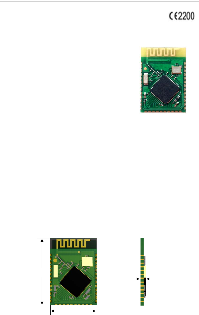
5. Size: 15 mm×22 mm×2.0mm
Mechanical Drawing
15mm
22mm 2mm
BEIJING JIA AN ELECTRONICS TECHNOLOGY CO.,LTD. AN2640SA-B Module Datasheet V1.0
http://www.rf-products.com Oct 28th 2015
Page 2 of 5
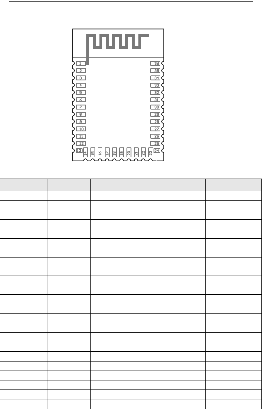
Terminal Description
Pad Number Name Description Pin Type
1 DIO0 GPIO, Sensor Controller Digital I/O
2 DIO1 GPIO, Sensor Controller Digital I/O
3 DIO2 GPIO, Sensor Controller Digital I/O
4 DIO3 GPIO, Sensor Controller Digital I/O
5 DIO4 GPIO, Sensor Controller Digital I/O
6 DIO5 GPIO, Sensor Controller, High drive
capacity
Digital I/O
7 DIO6 GPIO, Sensor Controller, High drive
capacity
Digital I/O
8 DIO7 GPIO, Sensor Controller, High drive
capacity
Digital I/O
9 GND Connect to GND Ground pin
10 VDD 1.8V to 3.8V main chip supply Power
11 DIO8 GPIO Digital I/O
12 DIO9 GPIO Digital I/O
13 DIO10 GPIO Digital I/O
14 DIO11 GPIO Digital I/O
15 DIO12 GPIO Digital I/O
16 DIO13 GPIO Digital I/O
17 DIO14 GPIO Digital I/O
18 DIO15 GPIO Digital I/O
19 JTAG-TMSC JTAG TMSC, High drive capability Digital I/O
20 JTAG-TCKC JTAG TCKC Digital I/O
BEIJING JIA AN ELECTRONICS TECHNOLOGY CO.,LTD. AN2640SA-B Module Datasheet V1.0
http://www.rf-products.com Oct 28th 2015
Page 3 of 5
21 DIO16 GPIO,High drive capability, JTAG_TDO Digital I/O
22 DIO17 GPIO, High drive capability, JTAG_TDI Digital I/O
23 DIO18 GPIO Digital I/O
24 DIO19 GPIO Digital I/O
25 DIO20 GPIO Digital I/O
26 DIO21 GPIO Digital I/O
27 DIO22 GPIO Digital I/O
28 RESET_N Reset, active-low. No internal pullup Digital input
29 DIO23 GPIO, Sensor Controller, Analog Digital/Analog I/O
30 DIO24 GPIO, Sensor Controller, Analog Digital/Analog I/O
31 DIO25 GPIO, Sensor Controller, Analog Digital/Analog I/O
32 DIO26 GPIO, Sensor Controller, Analog Digital/Analog I/O
33 DIO27 GPIO, Sensor Controller, Analog Digital/Analog I/O
34 DIO28 GPIO, Sensor Controller, Analog Digital/Analog I/O
35 DIO29 GPIO, Sensor Controller, Analog Digital/Analog I/O
36 DIO30 GPIO, Sensor Controller, Analog Digital/Analog I/O
Specifications
Parameter Min Max Unit
Operating Voltage 1.8 3.8 V
Operating Temperature -40 85 ℃
Current
Consumption
BLE Advertising
(Interval 100mS) 0.23 - mA
BLE
Connection
Interval 30mS 0.35 - mA
Interval 50mS 0.22 - mA
Interval 100mS 0.12 - mA
Interval 500mS 0.02 - mA
Sleep mode - 1 µA
TX Power -21 +5 dBm
RX Sensitivity -87 -96 dBm
Storage Temperature -40 150 ℃
BEIJING JIA AN ELECTRONICS TECHNOLOGY CO.,LTD. AN2640SA-B Module Datasheet V1.0
http://www.rf-products.com Oct 28th 2015
Page 4 of 5
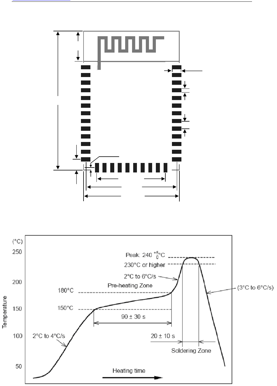
Recommended PCB Layout for Package
Soldering Recommendations
11.43mm
16mm
23mm
5mm
1.77mm
0.4mm
1.27mm
0.7mm
1.6mm
15.2mm

BEIJING JIA AN ELECTRONICS TECHNOLOGY CO.,LTD. AN2640SA-B Module Datasheet V1.0
http://www.rf-products.com Oct 28th 2015
Page 5 of 5
The AN2640SA-B module is designed to comply with the FCC statement. FCC ID is VVJ-AN264
0SA-B. The host system using AN2640SA-B, should have label indicated FCC ID VVJ-AN2640S
A-B.
This radio should NOT be installed and operating simultaneously with other radio
FCC STATEMENT
§ 15.21 Information to user.
Any Changes or modifications not expressly approved by the party responsible for compliance co
uld void the user's authority to operate the equipment.
§ 15.105 Information to the user.
Note: This equipment has been tested and found to comply with the limits for a Class B digital dev
ice, pursuant to part 15 of the FCC Rules. These limits are designed to provide reasonable protecti
on against harmful interference in a residential installation. This equipment generates uses and can
radiate radio frequency energy and, if not installed and used in accordance with the instructions,
may cause harmful interference to radio communications. However, there is no guarantee that inte
rference will not occur in a particular installation. If this equipment does cause harmful interferenc
e to radio or television reception, which can be determined by turning the equipment off and on, th
e user is encouraged to try to correct the interference by one or more of the following measures:
-Reorient or relocate the receiving antenna.
-Increase the separation between the equipment and receiver.
-Connect the equipment into an outlet on a circuit different from that to which the receiver is conn
ected.
-Consult the dealer or an experienced radio/TV technician for help.
*RF warning for Mobile device:
This equipment complies with FCC radiation exposure limits set forth for an uncontrolled environ
ment. This equipment should be installed and operated with minimum distance 20cm between the
radiator & your body.
§ 15.19 Labelling requirements.
This device complies with part 15 of the FCC Rules. Operation is subject to the following two
conditions: (1) This device may not cause harmful interference, and (2) this device must accept
any interference received, including interference that may cause undesired operation.