Beijing Jia An Electronic Technology Co ZB2530UPA-A Zigbee Module User Manual
Beijing Jia An Electronic Technology Co,. Ltd Zigbee Module
User Manual
ZB2530UPA-A Module Datasheet V1.0
May 24 2017
—————————————————————————————————————————————
Page - 1 -of 6
ZB2530UPA-A Module Datasheet V1.0
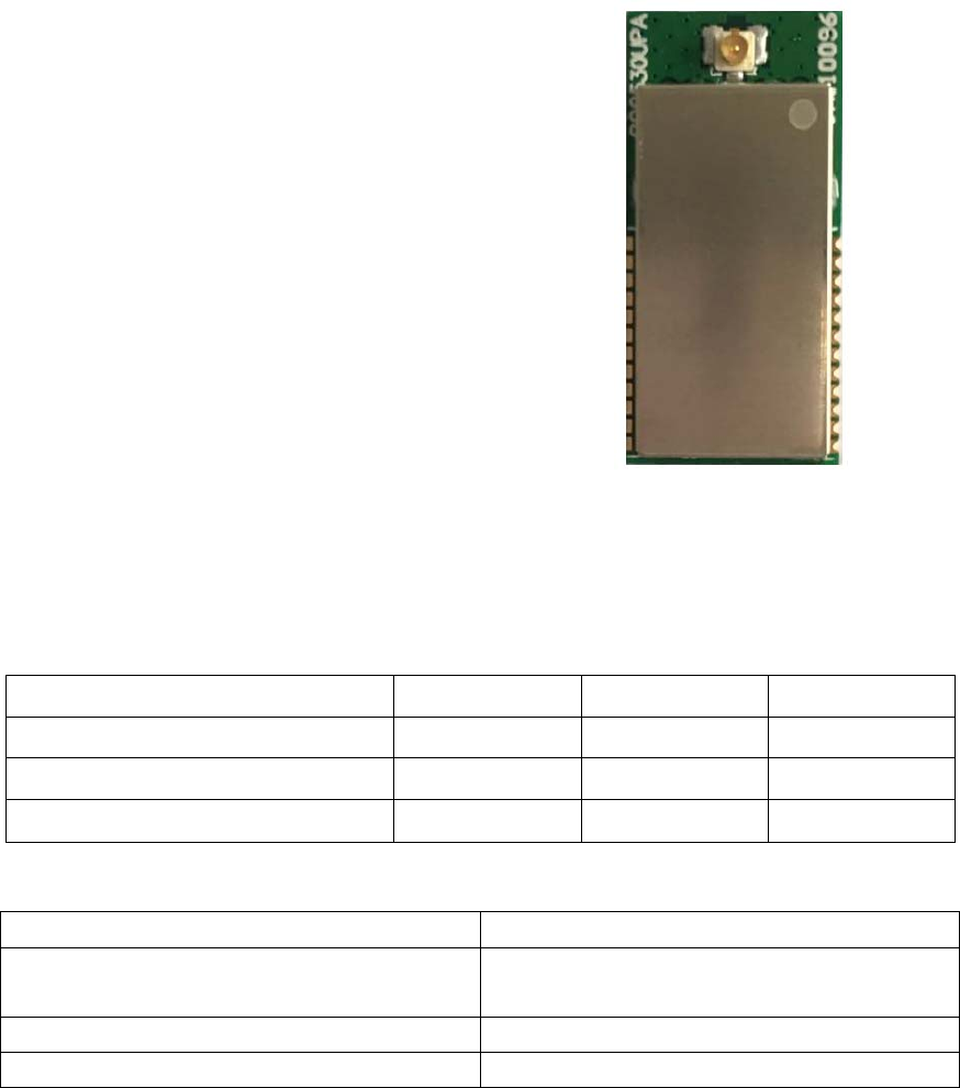
Introduction
The CC2530 is a system-on-chip (SoC) solution for
IEEE 802.15.4, Zigbee, and RF4CE applications.
The CC2530 combines the excellent performance of
a leading RF transceiver with an industry-standard
enhanced 8051 MCU, in-system programmable
Flash memory, 8-KB RAM, and many other powerful
features.
This chip enables industrial grade applications by
offering state-of-the-art selectivity and co-existence,
excellent link budget, and low-voltage operation.
The CC2591 is a range extender for 2.4GHz RF
transceivers, transmitters, and SoC products from
Texas Instruments. The CC2591 increases the RF
link budget by providing a Power Amplifier (PA) for
higher output power and a Low Noise Amplifiler
(LNA) for improved receiver sensitivity. The CC2591
contains RF switches, RF matching, and an on-chip
balun for a seamless interface with the CC2530.
This allows for a simple design of high performance
wireless applications.
Characteristics
Recommended Operating Conditions
Parameter Min Max Unit
Operating Frequency 2405 2480 MHz
Operating Supply Voltage 2.0 3.6 V
Operating Temperature -40 125
℃
Radio Characteristics
Parameter Specifications
Current Consumption TX:166mA
RX:24~27mA
RX Sensitivity HGM -98.8dBm
RX Sensitivity LGM -90.4dBm
ZB2530UPA-A Module Datasheet V1.0
May 24 2017
—————————————————————————————————————————————
Page - 2 -of 6
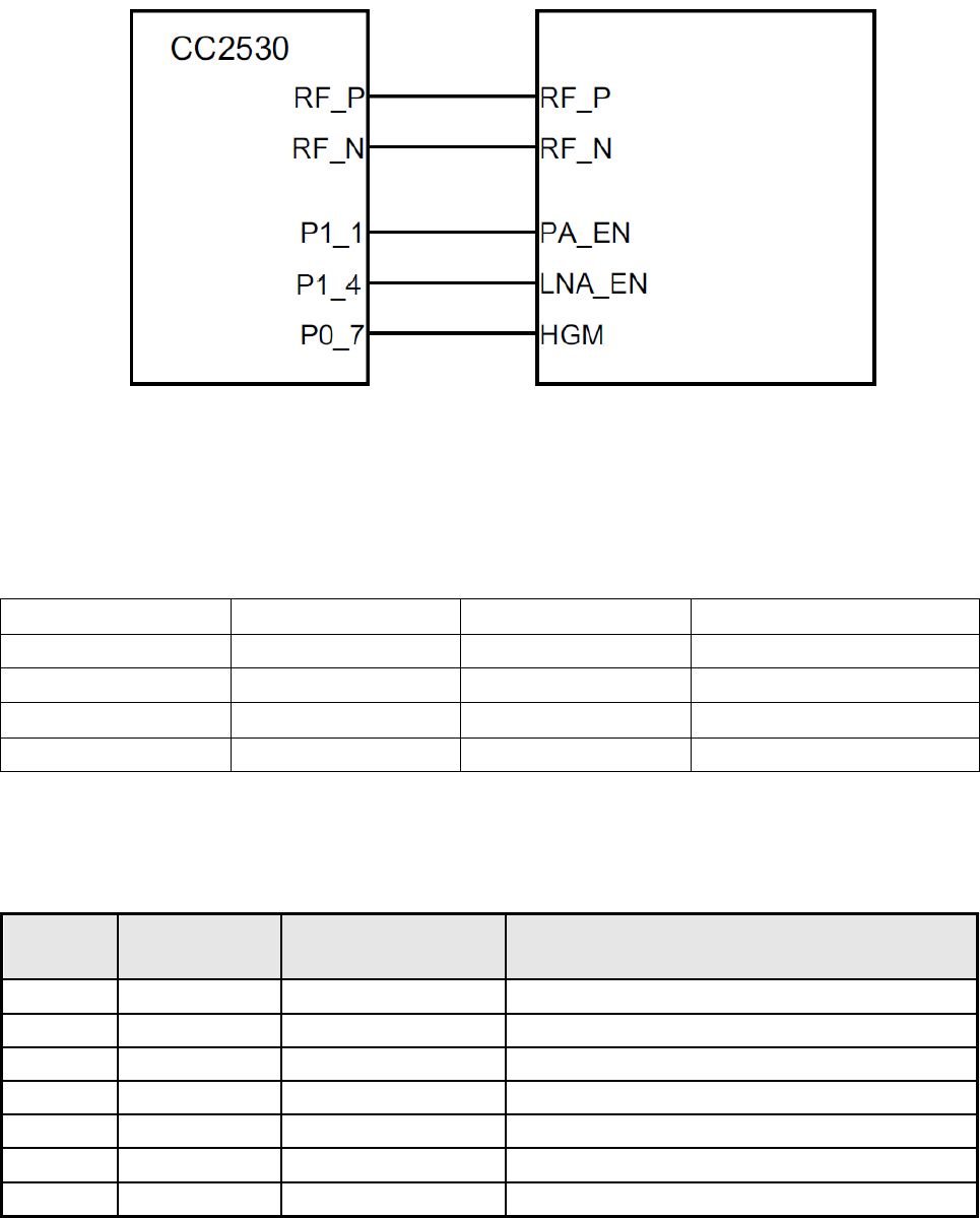
Functional Block Diagram
Control Logic for connecting the CC2591 to a CC2530 Device
There are three digital control pins(PA_EN, LNA_EN and HGM) on the CC2591 that control the state of the
chip. The bellowing table shows the control logic when connecting the CC2591 to a CC2530 device.
PA_EN LAN_EN HGM Mode of Operation
0 0 X Power Down
0 1 0 RX Low Gain Mode
0 1 1 RX High Gain Mode
1 0 X TX
Terminal Description
Pad
Number Name Pin Type Description
1 P2_2 Digital I/O Port 2.2
2 P2_1 Digital I/O Port 2.1
3 P2_0 Digital I/O Port 2.0
4 P1_7 Digital I/O Port 1.7
5 P1_6 Digital I/O Port 1.6
6 P1_5 Digital I/O Port 1.5
7 P1_4 Digital I/O Port 1.4
CC2591
ZB2530UPA-A Module Datasheet V1.0
May 24 2017
—————————————————————————————————————————————
Page - 3 -of 6
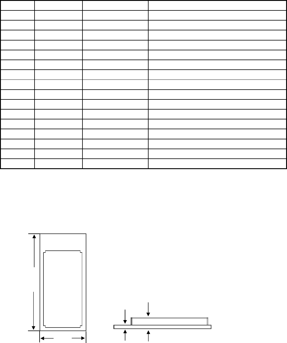
Mechanical Drawing
IMPORTANT NOTE:
This module has been granted as Single modular approval.
8 P1_3 Digital I/O Port 1.3
9 P1_2 Digital I/O Port 1.2
10 P1_1 Digital I/O Port 1.1, 20mA drive capability
11 P1_0 Digital I/O Port 1.0, 20mA drive capability
12 P0_7 Digital I/O Port 0.7
13 GND Ground Pin Connect to GND
14 GND Ground Pin Connect to GND
15 P0_6 Digital I/O Port 0.6
16 P0_5 Digital I/O Port 0.5
17 P0_4 Digital I/O Port 0.4
18 P0_3 Digital I/O Port 0.3
19 P0_2 Digital I/O Port 0.2
20 P0_1 Digital I/O Port 0.1
21 P0_0 Digital I/O Port 0.0
22 RESET_N Digital Input Reset, active-low
23 VDD Power 2V to 3.6V main chip supply
24 VDD Power 2V to 3.6V main chip supply
15.0
31..5
1.0
3.0
Unit:mm
Tolerance:±0.2mm

ZB2530UPA-A Module Datasheet V1.0
May 24 2017
—————————————————————————————————————————————
Page - 4 -of 6
The manufacturer is responsible to follow the instruction hereafter for the FCC compliance
requirement of the end product. Under such configuration, the FCC radiation exposure limits
set forth for an population/uncontrolled environment can be satisfied. The device with a Monopole
antenna gain with maximum gain 3.5dBi.
This device may only operate using an antenna of a type and maximum (or lesser) gain
approved by Beijing Jia An Electronics Thechnology Co,.Ltd, Antenna types difference or
having a gain greater than the maximum gain indicated for that type are strictly prohibited for
use with this transmitter.
Warning:
Any Changes or modifications not expressly approved by the party responsible for compliance
could void the user's authority to operate the equipment.
This device complies with part 15 of the FCC Rules. Operation is subject to the following two
conditions: (1) This device may not cause harmful interference, and (2) this device must accept
any interference received, including interference that may cause undesired operation.
Note: This equipment has been tested and found to comply with the limits for a Class B digital
device, pursuant to part 15 of the FCC Rules. These limits are designed to provide
ZB2530UPA-A Module Datasheet V1.0
May 24 2017
—————————————————————————————————————————————
Page - 5 -of 6
reasonable protection against harmful interference in a residential installation. This
equipment generates, uses and can radiate radio frequency energy and, if not installed and
used in accordance with the instructions, may cause harmful interference to radio
communications. However, there is no guarantee that interference will not occur in a
particular installation. If this equipment does cause harmful interference to radio or television
reception, which can be determined by turning the equipment off and on, the user
is encouraged to try to correct the interference by one or more of the following measures:
—Reorient or relocate the receiving antenna.
—Increase the separation between the equipment and receiver.
—Connect the equipment into an outlet on a circuit different from that to which the receiver is
connected.
—Consult the dealer or an experienced radio/TV technician for help.
FCC Radiation Exposure Statement:
This equipment complies with FCC radiation exposure limits set forth for an uncontrolled
environment .
This transmitter must not be co-located or operating in conjunction with any other antenna or
transmitter.
This equipment should be installed and operated with minimum distance 20cm between the
radiator& your body.
ZB2530UPA-A Module Datasheet V1.0
May 24 2017
—————————————————————————————————————————————
Page - 6 -of 6
This radio transmitter (identify the device by certification number) has been approved by FCC
to operate with the antenna types with the maximum permissible gain indicated.
The final end product must be labeled in a visible area with the following: Contains Transmitter
Module FCC ID:VVJ-ZB2530UPA-A