Bird Technologies Group 5PI001103 One-Way Signal Booster Amplifier User Manual 9257 s1 1
Bird Technologies Group One-Way Signal Booster Amplifier 9257 s1 1
users manual
EXHIBIT 2 PAGE 1 OF 17
TX RX Systems Inc. Manual 7-9257 (version 1) 11/03/00 Page 1
7-9257-1
Installation and Setup Manual
for the One-way Signal Booster System
Model Number 60-96-00400-G1
First Printing: November 2000
Version Number Version Date
1 11/03/00
82NCB
Part No.
Copyright (c) 2000 TX Rx Systems, Inc.

EXHIBIT 2 PAGE 2 OF 17
TX RX Systems Inc. Manual 7-9257 (version 1) 11/03/00 Page 2
WARRANTY
This warranty applies for one year from shipping date.
TX RX SYSTEMS INC. warrants its products to be free from defects in material and workman-
ship at the time of shipment. Our obligation under warranty is limited to replacement or repair at
our option, of any such products (with the exception of tubes) which shall have been defective at
the time of manufacture. TX RX SYSTEMS INC. reserves the right to replace with merchandise
of equal performance although not identical in every way to that originally sold. TX RX SYS-
TEMS INC. is not liable for damage caused by lightning or other natural disasters. No product
will be accepted for repair or replacement without our prior written approval.
All Shipping charges on returned products must be prepaid by the purchaser. TX RX SYSTEMS
INC. shall in no event be liable for consequential damages, installation costs or expenses of any
nature resulting from the purchase or use of products, whether or not they are used in accordance
with instructions. This warranty is in lieu of all other warranties, either expressed or implied,
including any implied warranty of merchantability or of fitness. No representative is authorized to
assume for TX RX SYSTEMS INC. any other liability or warranty than set forth above in connec-
tion with our products or services.
EXHIBIT 2 PAGE 3 OF 17
TX RX Systems Inc. Manual 7-9257 (version 1) 11/03/00 Page 3
Table of Contents
General Description 4
Note About Output Power Rating 5
Installation
Cautionary Note
Pre-RF Connection Tests 6
Test Equipment
Antenna Isolation 7
Procedure for Measuring Antenna Isolation
Increasing Isolation
Input Signal Levels
Procedure for Measuring Input Signal Levels 8
Reduction of Incoming Signal Strength 9
Setting Signal Booster Gain
Gain Reduction Methods
Bypassing Amplifier Stages
Operation
Performance Survey 10
Maintenance and Repair
Detailed Subassembly Descriptions 11
Preselector Assembly 3-14478
OLC Assembly 3-9417 12
Pre-Amplifier 3-11432 13
First Driver Amplifier 3-11432 14
Second Driver Amplifier3-11795
Power Amplifier 3-3948
illustrations & Tables
Figure 1 Inside view of the Model 60-96-00400-G1 4
Figure 2 Measuring Antenna Isolation 6
Figure 3 Measuring Input Signal Levels 8
Figure 4 Measuring Signal Booster Gain 10
Figure 5 Surveying Performance 11
Figure 6 OLC Assembly 3-9417 12
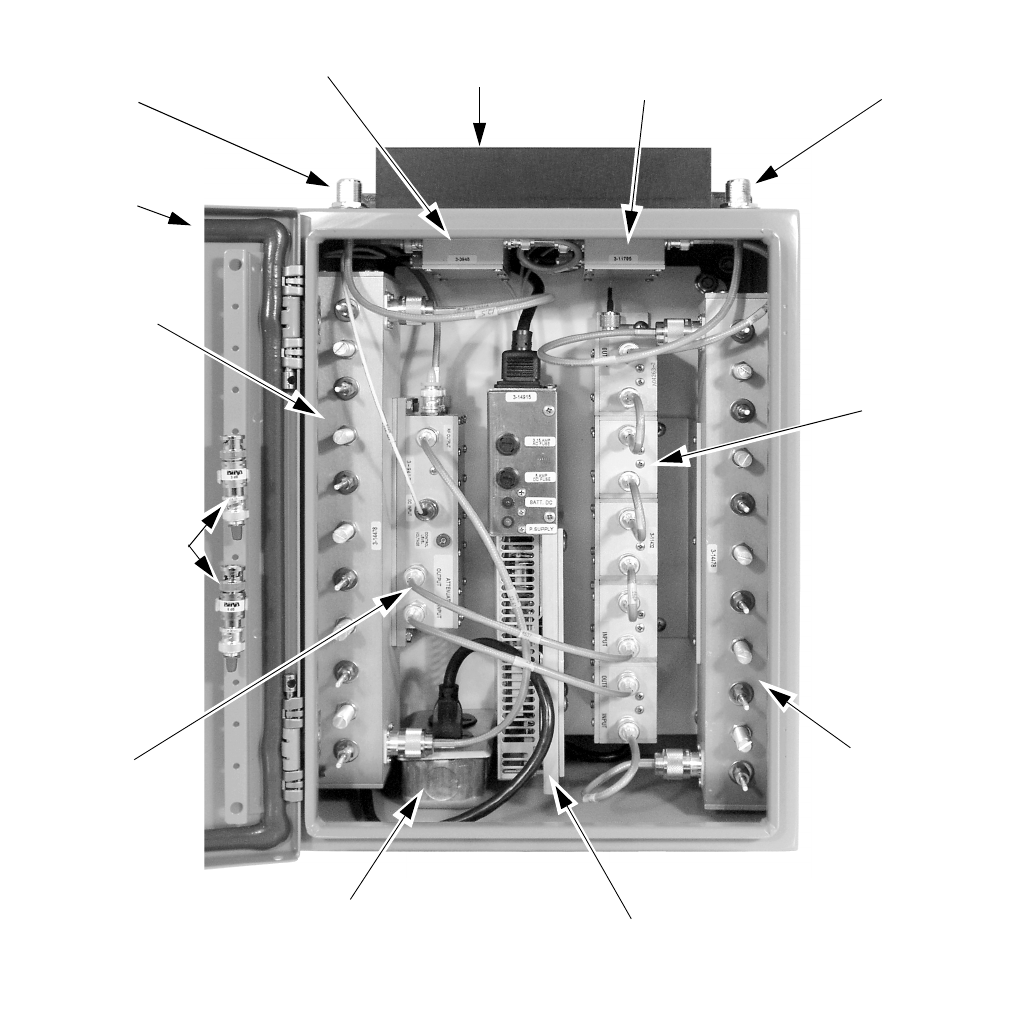
EXHIBIT 2 PAGE 4 OF 17
TX RX Systems Inc. Manual 7-9257 (version 1) 11/03/00 Page 4
GENERAL DESCRIPTION
Signal boosters extend radio coverage into areas
where abrupt propagation losses prevent reliable
communication. This system receives an RF sig-
nal, raises its power level, and couples it to an
antenna or leaky (radiating) coaxial cable system
so that it can be re-radiated. No frequency transla-
tion (conversion) occurs with this device.
The one-way signal booster model 60-96-00400-
G1 (shown in figure 1) is a broadband, bidirectional
single branch system which passes frequencies
from 929 to 932 MHz. The system covers a 3 MHz
passband width (factory set) and uses linear RF
active amplifiers, filters, and DC power sources to
adequately boost and re-radiate the passband sig-
nals.
The output level of any signal passing through a
signal booster is determined by the systems gain
specification. All signals passing through a prop-
erly operating signal booster are amplified by the
Figure 1: Inside view of the model 60-96-00400-G1 one-way signal booster system.
Output
Port
Door
Input
Preselector
3-14478
3 and 6 dB Fixed
Attenuator Pads
OLC
Assembly
AC
Receptacle
Power
Supply
3-14915
Output
Preselector
3-14478
1 and 4 Stage
Amplifier
3-11432
Input
Port
3 Watt
Amplifier
3-11795
Heatsink
6 Watt
Amplifier
3-3948
3-9417
EXHIBIT 2 PAGE 5 OF 17
TX RX Systems Inc. Manual 7-9257 (version 1) 11/03/00 Page 5
same amount but will come out at power levels that
are related to their respective input level by the
gain specification. Signal leveling is not an
intended function of a signal booster. Amplifier
stages used in this signal booster system may be
damaged by excessively strong input signal levels.
The system is equipped with Output Leveling Cir-
cuitry (OLC) to protect the amplifiers and reduce
spurious signals. It is interesting to note that the
total power for the multicarrier condition is always
less than the maximum single carrier rating. As the
number of carriers increases, the difference
between the single carrier maximum and the total
power of all carriers grows even greater.
Linear power amplifiers (Class-A operation) are
used in this application in contrast to the highly effi-
cient Class-C power amplifiers used in the output
stages of most FM land mobile transmitters. Linear
amplifiers are biased for a relatively high continu-
ous DC current drain that does not change with
changing RF drive levels. Class-A amplifiers gener-
ally have the lowest efficiency of the various ampli-
fier types, typically in the range of 25 - 33%. Their
biggest advantage is faithful reproduction of the
input waveform which results in the lowest levels of
intermodulation distortion products (IM) of all the
classes of amplifiers. The generation of IM distor-
tion is a serious design consideration when two or
more channels are simultaneously present in the
same amplifier stage.
Filtering is used at the input and output of the sig-
nal path to help suppress any IM products that may
be inadvertently generated. Signals that exceed
the maximum input rating may either damage the
signal booster or cause it to generate intermodula-
tion products that exceed the maximum allowed by
the FCC or other regulatory agency.
Note About Output Power Ratings
A single maximum output power rating does not
apply to broadband signal boosters because the
linear amplifiers (Class A) used in them may have
to process multiple simultaneous signals. Under
these conditions, the questions of power rating
becomes more complex.
When more than one signal is amplified, a number
of spurious signals will also appear in the amplified
output. They are referred to as intermodulation dis-
tortion products, more commonly called IM. These
spurious products would not be present in a per-
fectly linear amplifier but as in all things, something
short of perfection is realized. Accepted industry
practice is to use the Third Order Intercept Point
specification of a signal booster to predict the level
of IM products. The intercept point is derived from
the measurement of an amplifiers 1 dB compres-
sion point.
INSTALLATION
The layout of the signal distribution system will be
the prime factor in determining the mounting loca-
tion of the signal booster enclosure. However,
safety and serviceability are also key consider-
ations. The unit should be located where it cannot
be tampered with by unauthorized personnel yet is
easily accessible to service personnel using trou-
ble shooting test equipment such as digital multim-
eters and spectrum analyzers. Also consider the
weight and size of the unit should it become
detached from its mounting surfaces for any rea-
son.
Very little is required to install this signal booster.
The unit should be bolted in its permanent position
using lag bolts or other suitable fasteners. Make
sure there is an unobstructed airflow over the
external heatsink. Safety and serviceability are key
considerations. The signal booster cabinet will stay
warm during normal operation so in the interest of
equipment longevity, avoid locations that will
expose the cabinet to direct sun or areas where the
temperature is continually elevated.
The signal booster is designed to be powered from
120 VAC and a conduit entry box is provided at the
bottom of the enclosure for bringing the AC line into
the cabinet. AC line connections should be made in
accordance with local electrical and building codes.
Connection of RF to the unit is made via “N” female
connectors located on top of the cabinet. These
connectors are individually labeled “Input” and
“Output”. Care should be used when making con-
nections to these ports to insure the correct
antenna cable is connected to its corresponding
input / output port or the system will not work. The
use of high quality connectors with gold center pins
is advised. Flexible jumper cables made of high
quality coax are also acceptable for connecting to
rigid cable sections.
CAUTIONARY NOTE
The following cautions are not intended to frighten
the user but have been added to make you aware
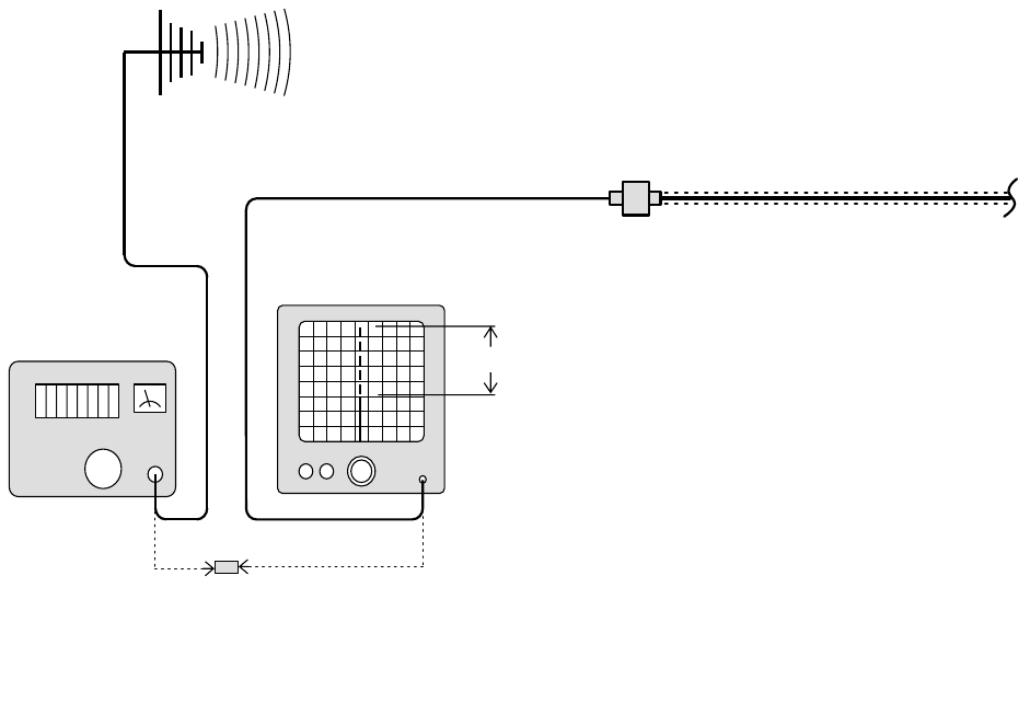
EXHIBIT 2 PAGE 6 OF 17
TX RX Systems Inc. Manual 7-9257 (version 1) 11/03/00 Page 6
of and help you to avoid the areas where experi-
ence has shown us that trouble can occur.
1) Just like the feedback squeal that can occur
when the microphone and speaker get too
close to each other in a public address system,
a signal booster can start to self oscillate. This
will occur when the isolation between the input
antenna or signal source and the output distri-
bution system does not exceed the signal
boosters gain by at least 15 dB. This condition
will reduce the effectiveness of the system and
may possibly damage the power amplifier
stages.
2) The major cause of damage to signal boosters
is the application of input RF power levels in
excess of the maximum safe input. This can
happen inadvertently when connecting a signal
generator with full power out to one of the inputs
or by a very strong signal that is far stronger
than expected. Following the pre-RF connection
checks listed next will help to avoid these two
problems.
PRE-RF CONNECTION TESTS
Certain characteristics of the signal distribution
system should be measured before connecting it to
the signal booster. This step is necessary to insure
that no conditions exist that could possibly damage
the signal booster and should not be skipped for
even the most thoroughly designed system. Two
characteristics need to be measured; antenna iso-
lation and input signal levels.
Test Equipment
The following equipment is required in order to per-
form the pre-installation measurements.
1) Signal generator for the frequencies of interest
capable of a 0 dBm output level. Modulation is
not necessary.
2) Spectrum analyzer that covers the frequencies
of interest and is capable of observing signal
levels down to -100 dBm.
3) Double shielded coaxial test cables made from
RG142 or RG55 coaxial cable.
INTERNAL
SIGNAL DISTRIBUTION
SYSTEM
SPECTRUM
ANALYZER
EXTERNAL
ANTENNA
SIGNAL
GENERATOR
ZERO LOSS
REFERENCE
ISOLATION (dB)
Figure 2: Typical test equipment setup for measuring antenna isolation.

EXHIBIT 2 PAGE 7 OF 17
TX RX Systems Inc. Manual 7-9257 (version 1) 11/03/00 Page 7
Antenna Isolation
Antenna isolation is the signal path isolation
between the two sections of the signal distribution
system that are to be connected to the signal
boosters antenna ports. Lack of isolation between
the input and output antennas can cause the
amplifiers in the system to oscillate. This can hap-
pen at a high enough level to damage the power
amplifier stages. In general, if one or both antenna
ports are connected to sections of radiating coaxial
cable (lossy cable) the isolation will be more than
adequate because of the high coupling loss values
that are encountered with this type of cable. When
a network of antennas are used for the input and
output, this problem is much more likely. Isolation
values are relatively easy to measure with a spec-
trum analyzer and signal generator.
Procedure for Measuring Antenna Isolation
1) Set the signal generator for a 0 dBm output
level at the center frequency of the signal boost-
ers passband (930.5 MHz).
2) Set the spectrum analyzer for the same center
frequency and a sweep width equal to or just
slightly greater than the passband chosen in
step one.
3) Connect the test leads of the signal generator
and the spectrum analyzer together using a
female barrel connector (see figure 2). Observe
the signal on the analyzer and adjust the input
attenuator of the analyzer for a signal level that
just reaches the 0 dBm level at the top of the
graticule.
4) Referring to figure 2, connect the generator test
lead to one side of the signal distribution system
(external antenna) and the spectrum analyzer
lead to the other (internal distribution system)
and observe the signal level. The difference
between this observed level and 0 dBm is the
isolation between the sections. If the signal is
too weak to observe, the spectrum analyzer's
bandwidth may have to be narrowed and its
input attenuation reduced. Record the isolation
value. The isolation value measured should
exceed the amplifier gain figure by at least
15 dB.
It is wise to repeat the procedure listed above for
measuring antenna isolation, with the signal gener-
ator set to frequencies at the passbands edges
(929 and 932 MHz) in order to see if the isolation is
remaining relatively constant over the complete
width of the passband.
Increasing Isolation
If the measured isolation does not exceed the
amplifier gain figure by at least 15 dB then modifi-
cation of the signal distribution system is required.
Alternately, the gain of the signal booster can also
be reduced to insure the 15 dB specification is met.
If the isolation cannot be increased then the
amount of gain reduction required is determined as
shown in the following example.
Input Signal Levels
Excessive input signal levels can damage the sig-
nal booster. Although this problem is less severe in
OLC protected systems, strong signals may cause
sudden reductions in gain and an associated
decrease in the desired output signal strength.
Even in the most carefully designed signal distribu-
tion systems, unpredictable situations can arise
that can cause this trouble. A few of the more com-
mon causes are:
a) Unintended signals entering the system. Prima-
rily caused by radios operating on channels that
are within the operational bandwidth of the sig-
nal booster. Sometimes this will be a transient
problem caused by mobile units when they
transmit while in close proximity to your system.
b) Hand-held and mobile units that approach
much closer than expected to one of the anten-
nas in the signal distribution system.
c) Unexpected signal propagation anomalies.
Building geometry can cause signal ducting and
other phenomena that cause signal levels that
are much stronger (or lower) than expected.
d) Lower than estimated signal attenuation causes
signals to be unusually strong. Higher losses
EXAMPLE
Gain Reduction (dB) = Minimum Isolation (dB) -
Measured Isolation (dB)
If the measured isolation is -75dB and the mini-
mum isolation is -80dB then the amount of gain
reduction required is: -80dB - (-75) = -5 dB
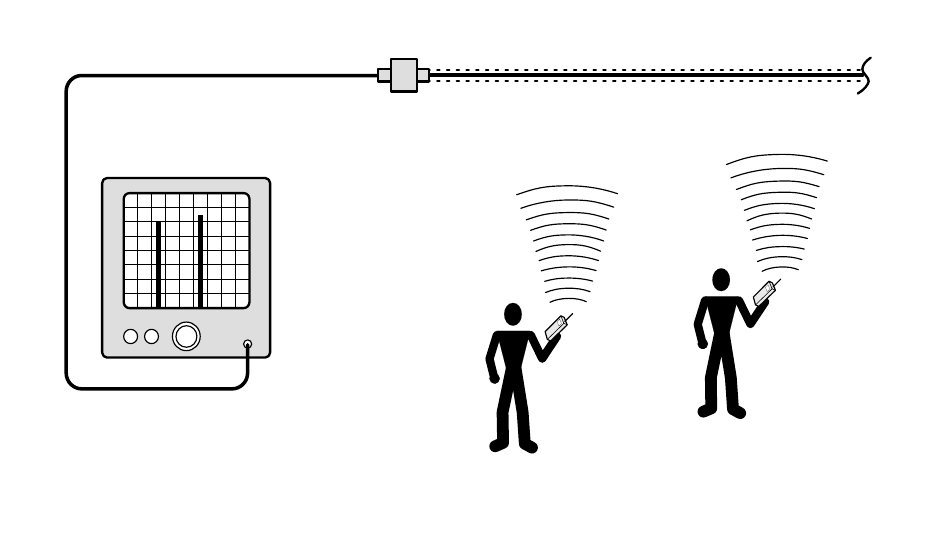
EXHIBIT 2 PAGE 8 OF 17
TX RX Systems Inc. Manual 7-9257 (version 1) 11/03/00 Page 8
can also occur giving weaker signals than
desired.
e) Signal booster model with excessive gain. In
systems that have an existing signal booster, it
is sometimes assumed that an identical unit
should be installed when expanding the system
to provide extended coverage. In most cases, a
signal booster with far less gain than the first is
required.
f) Improper installation or application of signal
splitters or directional couplers in the signal dis-
tribution system. This is usually the cause of too
low a signal level but deserves mentioning here.
Signal splitting needs to be done with constant
impedance signal splitters so that the proper
power splitting ratios and VSWR are main-
tained. Using tee connectors by themselves is
inviting trouble. Directional couplers must be
connected with regard to their directionality and
coupling levels or improper system signal levels
may result.
Procedure for Measuring Input Signal Levels
1) Set a spectrum analyzer for the center fre-
quency of the system (930.5 MHz).
2) Set the analyzers sweep width so that the entire
passband frequency range can be observed.
3) The analyzers input attenuator should be set to
observe input signal levels from approximately -
80 dBm to 0 dBm.
4) Connect the analyzer to the section of the sig-
nal distribution system that is going to serve as
the input (see figure 3).
5) Record the power level (in dBm) of all carriers in
the passband frequency range that are signifi-
cantly greater than the noise floor displayed on
the analyzer.
6) To find the total power being applied the calcu-
lations listed below must be performed. The
conversion chart at the rear of the manual can
be used. Here are the steps:
a) Convert all values in dBm to Watts
b) Total the power for all carriers in Watts
c) Convert the total power in Watts to dBm
Example: suppose we have a signal booster with a
maximum gain of 70 dB. After checking the input
signal levels, it was determined that there are three
signals that are significantly greater than the noise
floor displayed on the analyzer. These signals have
strengths of -45 dBm, -43 dBm and -41 dBm.
S p e c t r u m A n a l y z e r
R a d i o 1
R a d i o 2
S I G N A L D I S T R I B U T I O N S Y S T E M
Figure 3: Typical test equipment setup for measuring input signal levels.

EXHIBIT 2 PAGE 9 OF 17
TX RX Systems Inc. Manual 7-9257 (version 1) 11/03/00 Page 9
First we use the conversion chart at the end of this
manual to convert the power levels in dBm to watts
so that we can add them together. The power in
watts is written in scientific notation but the chart
uses computer notation. For example, in the chart,
an exponent may be written as E-08. In conven-
tional mathematical notation E-08 is written 10-8.
The total power must be written as a number
between 0 and 10 to use the chart. Look up
1.611E-7 in the Watts column. This number falls
between -38 and -37 dBm so we chose -37
because it is the next higher value.
Reduction of Incoming Signal Strength
Reducing the strength of offending signals may
require some or all of the following steps:
a) The addition of extra filtering. Consult TX RX
System's sales engineers for help in this
respect.
b) Modification of the signal distribution layout by
changing the type or location of pickup anten-
nas. This has to be approached in an empirical
way, that is, change-and-try until you get the
desired results. Sometimes changing from omni
to directional antennas will correct the problem.
Setting Signal Booster Gain
The Pre-Installation checks as outlined earlier
should have been performed to determine if gain
reduction will be necessary for your installation.
This can be due to low antenna isolation or exces-
sive input signal levels, or both. The actual amount
of gain reduction is determined by the largest num-
ber required because of either low isolation or
excessive signal levels.
For example, if the results of the isolation measure-
ment indicated the need for a gain reduction of -10
dB but signal level measurements indicate a need
for only a -5 dB gain reduction; then 10 dB is the
number required since both conditions are satis-
fied.
Gain Reduction Methods
As shipped from the factory, the system was setup
for maximum gain. Gain reduction is accomplished
by adding fixed attenuator pads to the input of the
pin diode attenuator section of the OLC assembly
or where even greater reductions are required,
bypassing one of the first driver amp stages.
Bypassing of amplifier stages is preferred for large
gain reductions so that excessive noise levels are
not produced. Use of attenuator pads alone will
reduce gain but the signal booster will also amplify
the noise generated in the lower level stages. The
correct positions for adding fixed pads to the sys-
tem are shown as dotted symbols on the specifica-
tion drawings.
CAUTION: Any fixed attenuator pads that are
already connected into the booster circuitry have
been installed at the factory and should not be
removed for any reason. Their function may be
other than gain reduction.
A pair of fixed attenuator pads (3 and 6 dB) are
supplied which are mounted in holders on the
inside of the cabinets front door. The pads’ attenu-
ation values are clearly labeled on the body of the
attenuator.
Bypassing Amplifier Stages
Sometimes the amount of gain reduction needed is
greater than the amount available with the attenua-
tor pads alone. In this case, the second stage of
the first driver amplifier may be bypassed. The five
stages of the amp are connected together with
short lengths of coaxial cable. To bypass the sec-
ond stage, remove the coax cable that connects
the second and third stages. Move the cable from
the input connector on the second stage to the cor-
responding connector on the third stage. The input
connector is always the one on the left when facing
the side of the amplifier with the BNC connectors.
Keep in mind that the total gain reduction is the
sum of the added pading plus the loss of gain for
the bypassed amplifier stage. Quality 50 ohm ter-
minations should be installed on the open termi-
nals of any bypassed stage.
OPERATION
Power is applied to the signal booster by turning on
the power supply assembly (see figure 1). The
green LED indicator should come on indicating the
Power (dBm) Power (watts)
-45 dBm 3.16 x 10⁻⁸
-43 dBm 5.01 x 10⁻⁸
-41 dBm 7.94 x 10⁻⁸
TOTAL 16.11 x 10⁻⁸
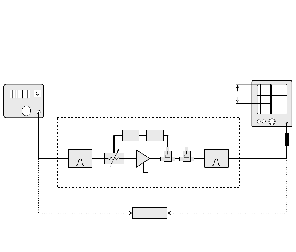
EXHIBIT 2 PAGE 10 OF 17
TX RX Systems Inc. Manual 7-9257 (version 1) 11/03/00 Page 10
power supply assembly is functioning normally.
The red LED is not used.
PERFORMANCE SURVEY
It is a good idea to document the performance of
the system after installation so that a reference
exists for future comparisons. This information can
make troubleshooting an interference problem or
investigation of a complaint about system perfor-
mance much easier. If there are coverage prob-
lems with a system, this survey will usually reveal
them allowing corrective measures to be taken
before the system is put into routine use. The fol-
lowing is an outline of how to do such a survey.
Because the nature of each installation can be
quite different, only a broad outline is given.
1) Measure the gain of the signal booster being
careful not to exceed the maximum input level.
Figure 4 shows this being done using a signal
generator and spectrum analyzer. This is basi-
cally a substitution measurement. Record the
measured values for each passband.
2) The signal booster system is equipped with a -
50 dB signal sampler port following the final out-
put amp (part of the OLC assembly). This port
is for the connection of test equipment such as
a spectrum analyzer and will allow the observa-
tion of the amplifier output at a considerably
reduced output level. This decoupling figure
needs to be added to a measured signal value
in order to arrive at the actual signal level.
3) With a spectrum analyzer connected to the sig-
nal sampler port (see figure 5), have personnel
with handheld radios move to predetermined
points and key their radios. Record the level of
these signals as observed on the analyzer and
also record the location of the person transmit-
ting. In this way, a map of the systems perfor-
mance can be generated.
4) For branches that amplify signals coming from a
fixed antenna or station, record the level of all
the desired incoming signals for future refer-
ence.
MAINTENANCE AND REPAIR
Signal boosters manufactured by TX RX Systems,
Inc. can function reliably for 10 or more years with
little or no maintenance. However, if the amplifiers
DC
Sampler Sampler
Detector
Electronic
Attenuator
OLC Assembly
Filter Filter
Amp
DC
Control
ZERO
REFERENCE
GAIN
10 dB Pad
SIGNAL
GENERATOR
SPECTRUM
ANALYZER
Figure 4: Test equipment interconnection for measuring signal booster gain.
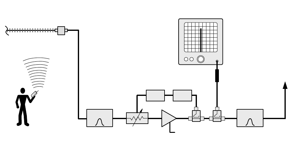
EXHIBIT 2 PAGE 11 OF 17
TX RX Systems Inc. Manual 7-9257 (version 1) 11/03/00 Page 11
are subjected to excessively high signal levels,
power surges or lightning strikes, failures may
occur. The following procedures may be followed
for detecting a malfunctioning unit or as part of a
periodic maintenance program.
1) The heatsink area should be cleared of dust
and debris.
2) Inspect the unit to see that the power supply
LED DC indicator is lit (remove any dust or
debris that may obscure the LED). This will ver-
ify that DC power is flowing properly. Check all
hardware for tightness.
3) Compare system performance to initial perfor-
mance levels measured when the system was
first installed. The lack of signal can be traced to
a malfunctioning amplifier by progressive signal
monitoring from the output (far end) to the input
end of the system noting the area where the
signal returns to normal level. The next amplifier
toward the output end of the system will proba-
bly be the one that failed.
or
Measure the gain at any convenient frequency
in the working frequency band to verify that the
gain specification is being met. If the gain val-
ues fall below that specified for the model check
the following:
A) Open the signal booster cabinet and inspect for
any loose or broken connections or cables, and
repair as necessary.
B) Measure the output of the power supply to see
that the proper operating voltage is being main-
tained.
C) If the operating voltage is proper but the gain is
still low, measure the gain of each amplifier
stage until the one with low gain is isolated.
Replace a low gain amplifier with a new ampli-
fier stage to correct the problem.
DETAILED SUBASSEMBLY DESCRIPTIONS
The following section details the operation of each
assembly in the One-Way Signal Booster System.
Preselector Assembly 3-14478
The RF input to the system is first applied to a
combline bandpass filter which limits the frequency
applied to all subsequent stages. The bandwidth of
this filter is determined by the spacing between the
tuning rods which are all located on one side of the
aluminum housing and vaguely resemble the teeth
of a comb (hence the name). This filter is consid-
ered to have one section for each tuning rod. the
greater the number of sections, the greater the
selectivity and ultimate rejection of the filter. These
filters are not intended for tuning to other frequency
DC
Sampler Sampler
Detector
Electronic
Attenuator
OLC Assembly
Filter Filter
Amp
DC
Control
10 dB Pad
SPECTRUM
ANALYZER
SIGNAL DISTRIBUTION SYSTEM
BOOSTED
RF SIGNA
L
Figure 5: Test equipment interconnection for surveying performance.
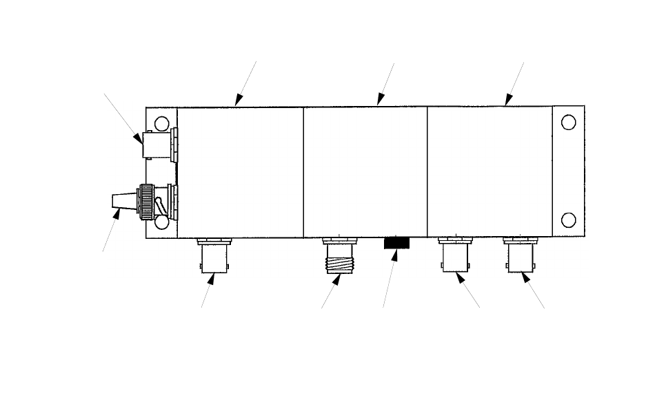
EXHIBIT 2 PAGE 12 OF 17
TX RX Systems Inc. Manual 7-9257 (version 1) 11/03/00 Page 12
bands. The combline output filters suppress any IM
products that may be inadvertently generated.
OLC Assembly 3-9417
Signals that exceed the maximum input rating may
either damage the repeater amplifier or cause it to
generate intermodulation products that exceed the
maximum allowed by the FCC or other regulatory
agencies. The addition of the Output Level Control
(OLC) circuit helps prevent this from happening.
The OLC Assembly (part # 3-9417) is set to main-
tain a maximum single carrier output power from
the 6-watt amplifier of +25 dBm. The assembly
contains a signal sampling and detection section, a
DC control section and a PIN diode RF attenuator
section which is applied ahead of all amplification.
OLC circuitry should not be considered a panacea
for a poor system design. One undesirable side
affect of OLC is that the signal level of all signals
being processed by the branch will be reduced
when this circuitry is activated. This means that the
performance of the system is actually decreased
for all signals in a branch as long as gain reduction
is taking place for any one signal in that branch.
The implication is that OLC has been designed to
handle short term or transient overdrive episodes
only.
This circuitry actuates when the predetermined
maximum output level is reached. The output
power level is sensed with a signal sampler that is
built into the OLC assembly. The sampler outputs
to a detector circuit which generates a DC voltage
that is proportional to the output power level. The
proportional DC voltage from the detector is then
applied to a control circuit which develops a voltage
used to control a variable electronic attenuator. The
electronically controlled attenuator is placed at the
input end of the amplifier chain and reduces the
incoming signal by an amount necessary to keep
the power from exceeding the maximum safe level.
The gain reduction range is typically 5 - 40 dB
which is more than adequate for most real life situ-
ations.
The OLC assembly is divided into three shielded
compartments; one housing the RF/DC converter,
the second a DC control circuit, and the third con-
taining the RF attenuator circuit. A test point is pro-
vided for measuring the DC voltage applied to the
RF attenuator (see figure 6). Regulated VDC is
RF to DC
Converter
DC Control
Circuit RF Attenuator
RF Input
RF Output
OLC
Voltage
Test Point
VDC
Input
RF Input
-50 dB
Sampler
Port
(Shown with
dustcover on)
RF Output
Figure 6: OLC Assembly 3-9417.
EXHIBIT 2 PAGE 13 OF 17
TX RX Systems Inc. Manual 7-9257 (version 1) 11/03/00 Page 13
supplied to a "TNC" female connector to power this
assembly.
The RF to DC converter section of the OLC assem-
bly contains three circuits, a -20 dB sampler which
is used to supply the RF signal to the diode detec-
tor, and finally a -50 dB sampler which provides a
convenience port for connecting test equipment.
The detector circuit receives RF from the -20 dB
sampler and produces a negative polarity DC out-
put voltage that is proportional to the RF signal. A
Schottky Barrier diode (D2) and integrator (R3/C1)
are used as the detector.
The DC voltage produced by the RF to DC con-
verter is directly proportional to the output signal
strength of the final amplifier. The DC voltage is
supplied to the DC control circuit at the non-invert-
ing terminal of op-amp IC2. A variable reference
DC voltage is applied to the inverting terminal of
the same op-amp. Variable resistor VR2 is used to
set the magnitude of this reference voltage and
controls the level at which gain reduction will start
to occur.
As the signal strength increases, the output voltage
of the RF to DC converter, which is of negative
polarity, becomes larger. This change causes the
output of IC2 to also become increasingly negative.
This output voltage is connected via diode D1 to
bias the RF attenuator circuit board assembly. As
this voltage becomes more negative, the attenua-
tion is increased thus achieving a certain range of
gain control. Diode D1 insures that the gain control
voltage is always positive and never goes below 0
volts. In actual practice, OLC operation is set to
commence when the power output of the final
amplifier reaches its maximum two-carrier level.
Two other ICs are mounted on the OLC control cir-
cuit board. IC1 is a 10 volt regulator that supplies
DC to the other two chips. Variable resistor VR1 is
used to set this voltage. IC3 is a voltage inverter
that produces -4.5 volts which is applied to the op-
amp IC2. This negative voltage allows the output
voltage of IC2 to closely approach 0 volts. Two
diodes (D1 and D2) are used in series to extend
the attenuation range. The diodes are always for-
ward biased with minimum forward resistance and
insertion loss occurring at about 20 ma of current.
Pre-Amplifier 3-11432
The pre-amplifier consists of the 400 milliwatt
amplifier connected between the input filter assem-
bly and the op-amp/attenuator assembly. The
preamplifier is a single stage of the five identical
stages found in assembly 3-11432 and is used to
insure that a sufficient level of signal is applied to
the attenuator.
Each of the five individual stages (part# 3-7718)
found in assembly 3-11432 are complete 400 milli-
watt amplifiers. They are mounted on a common
mounting panel and have a common DC distribu-
tion bus running internally between the individual
stages. Each stage provides a minimum of 13.2 dB
of gain with a power requirement of 21.7 VDC
(nominal) and a typical current draw of 120 ma.
The maximum single carrier power output is 400
milliwatts.
Each amplifier stage consists of two circuits, the
amplifier circuit (3-7725) and the bias regulator cir-
cuit (3-10742). Both of these circuits are housed in
their own enclosures which are then physically
joined together to make up one stage. The circuits
are electrically joined using feed-thru capacitors
Cf1 and Cf2.
The amplifier circuit uses a linear RF transistor Q1
(Philips part# BFQ34/01) which is operated in a
class "A" configuration in order to keep intermodu-
lation distortion to a minimum. The RF transistor is
biased for a nominal collector current of 120 ma. A
bias regulator circuit is used to keep the collector
current constant with changes in temperature. Nar-
row band matching techniques are used in this
amplifier and it will require tuning if the transistor or
matching network components are replaced.
The bias regulator circuit uses an Op-Amp compar-
ator IC1 to supply a variable bias current which var-
ies as required to keep the RF transistors collector
current constant. Current to the collector of the RF
transistor flows through resistor R1. The voltage at
the collector side of this resistor is applied to the
non-inverting input of IC1. Voltage divider R2 / R4
sets the desired reference voltage on the inverting
terminal of IC1. The variable output voltage at pin 6
of IC1 is then applied to the base of the RF transis-
tor. The bias on the RF transistor will now vary in
such a way as to keep the voltage at the collector
end of R1 equal to the reference voltage provided
by divider R2/R4, thus keeping the RF transistor's
collector current constant (120 ma nominal).
EXHIBIT 2 PAGE 14 OF 17
TX RX Systems Inc. Manual 7-9257 (version 1) 11/03/00 Page 14
Repair or replacement of bias circuit components
does not necessitate retuning of the amplifier.
First Driver Amplifier 3-11432
The remaining four stages of the five stage assem-
bly (3-11432) are used to form a driver amplifier
which amplifies the output of the OLC assembly
and applies it to the second driver amp.
Second Driver Amplifier 3-11795
The second driver amplifier is used to provide suffi-
cient amplification to drive the input of the final
amp. It uses a single ultra-linear RF transistor. The
2.5 watt rating indicates the maximum safe output
from this amplifier using a single carrier. The
actual maximum allowable power output with multi-
carriers is considerably lower and is determined by
the maximum allowable intermodulation product
level and is also limited by the collector-emitter
breakdown rating of the RF transistor.
This amplifier stage draws a nominal 500 ma. A
bias regulator circuit within the amplifier assembly
is used to keep the collector current of the RF tran-
sistor constant with changes in temperature. This
amplifier has a minimum gain of 14 dB, 15 dB typi-
cal. The amplifier uses narrow band matching tech-
niques and will require tuning if the transistor or
matching network components are replaced.
The bias regulator circuit uses an operational
amplifier and a PNP transistor to supply a variable
bias current that varies as required to keep the RF
transistor collector current constant. Current to the
collector of the RF transistor is sampled through
resistor R5. The voltage at the collector side of this
resistor is applied to the non-inverting input of U1.
Voltage divider R6 / R7 sets the desired reference
voltage on the inverting terminal of U1. U1 is lifted
above chassis ground by the zener diode D2 in
order to keep U1 operating below its 18 volt maxi-
mum rating.
Resistor R3 and C2 work in combination to pre-
vent U1 from oscillating at audio frequencies. The
variable output voltage of U1 biases pass transistor
Q1 through the voltage divider R4 / R8. Q1 in turn
supplies the current to bias the RF transistor. The
bias on the RF transistor varies in such a way as to
keep the voltage at the collector end of R5 equal to
the reference voltage provided by divider R6 / R7,
thus keeping the RF transistor's collector current
constant. Repair or replacement of bias circuit
components does not necessitate retuning of the
amplifier.
Power Amplifier 3-3948
This 6 watt final amplifier uses a single ultra-linear
RF transistor. The 6 watt rating indicates the maxi-
mum safe power output from this amplifier using a
single carrier. The actual maximum allowable
power output with multi-carriers is considerably
lower and is determined by the maximum allowable
intermodulation product level and is also limited by
the collector-emitter breakdown rating of the RF
transistor. The One-Way Signal Booster systems
power specifications appear on the specification
drawing.
This stage receives its DC power from the 21 volt
regulator and draws a nominal 960 ma. The RF
transistor is biased for a nominal collector current
of 880 ma. A bias regulator circuit is used to keep
the collector current constant with changes in tem-
perature. This stage has a minimum gain of 9 dB,
10 dB typical. This amplifier uses narrow band
matching techniques and will require tuning if the
transistor or matching network components are
replaced.
The bias regulator circuit uses an operational
amplifier and a PNP transistor to supply a variable
bias current that varies as required to keep the RF
transistor collector current constant. Current to the
collector of the RF transistor is sampled through
resistor R5. The voltage at the collector side of this
resistor is applied to the non-inverting input of U1.
Voltage divider R6 / R7 sets the desired reference
voltage on the inverting terminal of U1. U1 is lifted
above chassis ground by the zener diode D2 in
order to keep U1 operating below its 18 volt maxi-
mum rating.
Resistor R3 and C2 work in combination to pre-
vent U1 from oscillating at audio frequencies. The
variable output voltage of U1 biases pass transistor
Q1 through the voltage divider R4 / R8. Q1 in turn
supplies the current to bias the RF transistor. The
bias on the RF transistor varies in such a way as to
keep the voltage at the collector end of R5 equal to
the reference voltage provided by divider R6 / R7,
thus keeping the RF transistor's collector current
constant. Repair or replacement of bias circuit
components does not necessitate retuning of the
amplifier.

EXHIBIT 2 PAGE 15 OF 17
TX RX Systems Inc. Manual 7-9257 (version 1) 11/03/00 Page 15
dBm dBw Watts Volts (50Ω)
80 50 100000 2236.07
79 49 79432.82 1992.9
78 48 63095.74 1776.17
77 47 50118.72 1583.01
76 46 39810.72 1410.86
75 45 31622.78 1257.43
74 44 25118.86 1120.69
73 43 19952. 62 998.81
72 42 15848.93 890.19
71 41 12589.25 793.39
70 40 10000 707.11
69 39 7943.28 630.21
68 38 6309.57 561.67
67 37 5011.87 500.59
66 36 3981.07 446.15
65 35 3162.28 397.64
64 34 2511.89 354.39
63 33 1995.26 315.85
62 32 1584.89 281.5
61 31 1258.93 250.89
60 30 1000 223.61
59 29 794.33 199.29
58 28 630.96 177.62
57 27 501.19 158.3
56 26 398.11 141.09
55 25 316.23 125.74
54 24 251.19 112.07
53 23 199.53 99.88
52 22 158.49 89.02
51 21 125.89 79.34
50 20 100 70.71
49 19 79.43 63.02
48 18 63.1 56.17
47 17 50.12 50.06
46 16 39.81 44.62
45 15 31.62 39.76
44 14 25.12 35.44
43 13 19.95 31.59
42 12 15.85 28.15
41 11 12.59 25.09
dBm dBw Watts Volts (50Ω)
40 10 10 22.36
39 9 7.94 19.93
38 8 6.31 17.76
37 7 5.01 15.83
36 6 3.98 14.11
35 5 3.16 12.57
34 4 2.51 11.21
33 3 2 9.99
32 2 1.59 8.9
31 1 1.26 7.93
30 0 1 7.07
29 -1 0.79 6.3
28 -2 0.63 5.62
27 -3 0.5 5.01
26 -4 0.4 4.46
25 -5 0.32 3.98
24 -6 0.25 3.54
23 -7 0.2 3.16
22 -8 0.16 2.82
21 -9 0.13 2.51
20 -10 0.1 2.24
19 -11 0.08 1.99
18 -12 0.06 1.78
17 -13 0.05 1.58
16 -14 0.04 1.41
15 -15 0.03 1.26
14 -16 0.03 1.12
13 -17 0.02 1
12 -18 0.02 0.89
11 -19 0.01 0.79
10 -20 0.01 0.71
9 -21 0.01 0.63
8 -22 0.01 0.56
7 -23 0.01 0.5
6-24 00.45
5-25 0 0.4
4-26 00.35
3-27 00.32
2-28 00.28
1-29 00.25
Power Conversion Chart
dBm to dBw : Watts : Microvolts

EXHIBIT 2 PAGE 16 OF 17
TX RX Systems Inc. Manual 7-9257 (version 1) 11/03/00 Page 16
dBm dBw Watts uVolts (50Ω)
0 -30 1.0000E-03 223606.8
-1 -31 7.9433E-04 199289.77
-2 -32 6.3096E-04 177617.19
-3 -33 5.0119E-04 158301.49
-4 -34 3.9811E-04 141086.35
-5 -35 3.1623E-04 125743.34
-6 -36 2.5119E-04 112068.87
-7 -37 1.9953E-04 99881.49
-8 -38 1.5849E-04 89019.47
-9 -39 1.2589E-04 79338.69
-10 -40 1.0000E-04 70710.68
-11 -41 7.9433E-05 63020.96
-12 -42 6.3096E-05 56167.49
-13 -43 5.0119E-05 50059.33
-14 -44 3.9811E-05 44615.42
-15 -45 3.1623E-05 39763.54
-16 -46 2.5119E-05 35439.29
-17 -47 1.9953E-05 31585.3
-18 -48 1.5849E-05 28150.43
-19 -49 1.2589E-05 25089.1
-20 -50 1.0000E-05 22360.68
-21 -51 7.9433E-06 19928.98
-22 -52 6.3096E-06 17761.72
-23 -53 5.0119E-06 15830.15
-24 -54 3.9811E-06 14108.64
-25 -55 3.1623E-06 12574.33
-26 -56 2.5119E-06 11206.89
-27 -57 1.9953E-06 9988.15
-28 -58 1.5849E-06 8901.95
-29 -59 1.2589E-06 7933.87
-30 -60 1.0000E-06 7071.07
-31 -61 7.9433E-07 6302.1
-32 -62 6.3096E-07 5616.75
-33 -63 5.0119E-07 5005.93
-34 -64 3.9811E-07 4461.54
-35 -65 3.1623E-07 3976.35
-36 -66 2.5119E-07 3543.93
-37 -67 1.9953E-07 3158.53
-38 -68 1.5849E-07 2815.04
-39 -69 1.2589E-07 2508.91
dBm dBw Watts uVolts (50Ω)
-40 -70 1.0000E-07 2236.07
-41 -71 7.9433E-08 1992.9
-42 -72 6.3096E-08 1776.17
-43 -73 5.0119E-08 1583.02
-44 -74 3.9811E-08 1410.86
-45 -75 3.1623E-08 1257.43
-46 -76 2.5119E-08 1120.69
-47 -77 1.9953E-08 998.82
-48 -78 1.5849E-08 890.2
-49 -79 1.2589E-08 793.39
-50 -80 1.0000E-08 707.11
-51 -81 7.9433E-09 630.21
-52 -82 6.3096E-09 561.68
-53 -83 5.0119E-09 500.59
-54 -84 3.9811E-09 446.15
-55 -85 3.1623E-09 397.64
-56 -86 2.5119E-09 354.39
-57 -87 1.9953E-09 315.85
-58 -88 1.5849E-09 281.5
-59 -89 1.2589E-09 250.89
-60 -90 1.0000E-09 223.61
-61 -91 7.9433E-10 199.29
-62 -92 6.3096E-10 177.62
-63 -93 5.0119E-10 158.3
-64 -94 3.9811E-10 141.09
-65 -95 3.1623E-10 125.74
-66 -96 2.5119E-10 112.07
-67 -97 1.9953E-10 99.88
-68 -98 1.5849E-10 89.02
-69 -99 1.2589E-10 79.34
-70 -100 1.0000E-10 70.71
-71 -101 7.9433E-11 63.02
-72 -102 6.3096E-11 56.17
-73 -103 5.0119E-11 50.06
-74 -104 3.9811E-11 44.62
-75 -105 3.1623E-11 39.76
-76 -106 2.5119E-11 35.44
-77 -107 1.9953E-11 31.59
-78 -108 1.5849E-11 28.15
-79 -109 1.2589E-11 25.09
Power Conversion Chart
dBm to dBw : Watts : Microvolts

EXHIBIT 2 PAGE 17 OF 17
TX RX Systems Inc. Manual 7-9257 (version 1) 11/03/00 Page 17
dBm dBw Watts uVolts (50Ω)
-80 -110 1.0000E-11 22.36
-81 -111 7.9433E-12 19.93
-82 -112 6.3096E-12 17.76
-83 -113 5.0119E-12 15.83
-84 -114 3.9811E-12 14.11
-85 -115 3.1623E-12 12.57
-86 -116 2.5119E-12 11.21
-87 -117 1.9953E-12 9.99
-88 -118 1.5849E-12 8.9
-89 -119 1.2589E-12 7.93
-90 -120 1.0000E-12 7.07
-91 -121 7.9433E-13 6.3
-92 -122 6.3096E-13 5.62
-93 -123 5.0119E-13 5.01
-94 -124 3.9811E-13 4.46
-95 -125 3.1623E-13 3.98
-96 -126 2.5119E-13 3.54
-97 -127 1.9953E-13 3.16
-98 -128 1.5849E-13 2.82
-99 -129 1.2589E-13 2.51
-100 -130 1.0000E-13 2.24
-101 -131 7.9433E-14 1.99
-102 -132 6.3096E-14 1.78
-103 -133 5.0119E-14 1.58
-104 -134 3.9811E-14 1.41
-105 -135 3.1623E-14 1.26
-106 -136 2.5119E-14 1.12
-107 -137 1.9953E-14 1
-108 -138 1.5849E-14 0.89
-109 -139 1.2589E-14 0.79
-110 -140 1.0000E-14 0.71
-111 -141 7.9433E-15 0.63
-112 -142 6.3096E-15 0.56
-113 -143 5.0119E-15 0.5
-114 -144 3.9811E-15 0.45
-115 -145 3.1623E-15 0.4
-116 -146 2.5119E-15 0.35
-117 -147 1.9953E-15 0.32
-118 -148 1.5849E-15 0.28
-119 -149 1.2589E-15 0.25
dBm dBw Watts uVolts (50Ω)
-120 -150 1.0000E-15 0.22
-121 -151 7.9433E-16 0.2
-122 -152 6.3096E-16 0.18
-123 -153 5.0119E-16 0.16
-124 -154 3.9811E-16 0.14
-125 -155 3.1623E-16 0.13
-126 -156 2.5119E-16 0.11
-127 -157 1.9953E-16 0.1
-128 -158 1.5849E-16 0.09
-129 -159 1.2589E-16 0.08
-130 -160 1.0000E-16 0.07
-131 -161 7.9433E-17 0.06
-132 -162 6.3096E-17 0.06
-133 -163 5.0119E-17 0.05
-134 -164 3.9811E-17 0.05
-135 -165 3.1623E-17 0.04
-136 -166 2.5119E-17 0.04
-137 -167 1.9953E-17 0.03
-138 -168 1.5849E-17 0.03
-139 -169 1.2589E-17 0.03
-140 -170 1.0000E-17 0.02
-141 -171 7.9433E-18 0.02
-142 -172 6.3096E-18 0.02
-143 -173 5.0119E-18 0.02
-144 -174 3.9811E-18 0.01
-145 -175 3.1623E-18 0.01
-146 -176 2.5119E-18 0.01
-147 -177 1.9953E-18 0.01
-148 -178 1.5849E-18 0.01
-149 -179 1.2589E-18 0.01
-150 -180 1.0000E-18 0.01
Power Conversion Chart
dBm to dBw : Watts : Microvolts