Bwave Technology W2R Tortuga User Manual revised
Shanghai Bwave Technology Co.,Ltd. Tortuga Users Manual revised
UserManual.wiki
>
Bwave Technology
>
W2R User Manual
>
Users Manual revised
Contents
1.
Users Manual
2.
Users Manual revised
Users Manual revised
Navigation menu
Upload a User Manual
Namespaces
Wiki Guide
HTML
PDF
Info
Views
User Manual
Discussion / Help
Navigation
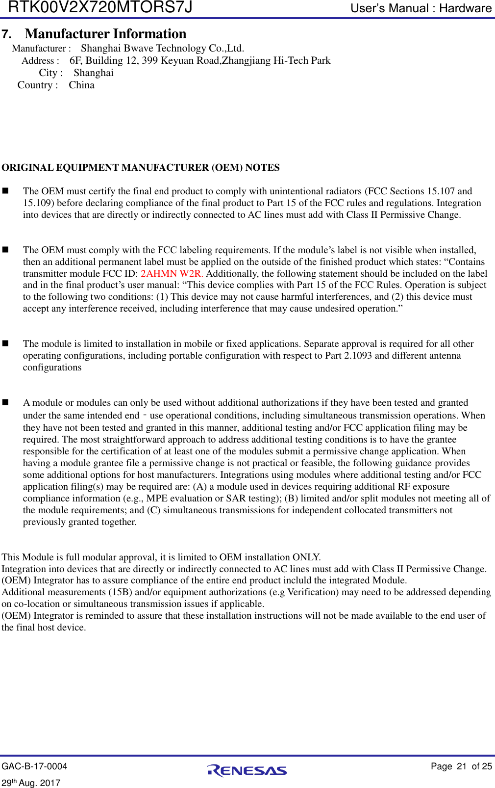
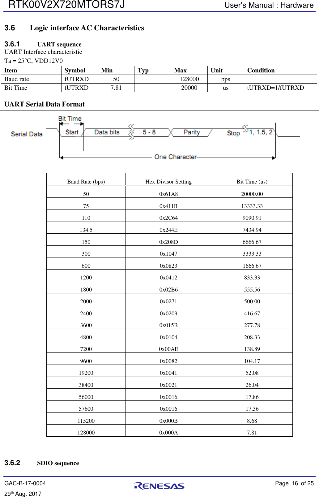
![RTK00V2X720MTORS7J User’s Manual : Hardware GAC-B-17-0004 Page 7 of 25 29th Aug. 2017 2.2 Mini PCIE pin information Pin Pin Name I/O Functional Description 1 RESERVE I/O - No connection(only connected to test pin) 2 RESERVE I/O - No connection 3 RESERVE I/O - No connection(only connected to test pin) 4 GND - GND GND 5 5.0V - Voltage Supply 5V voltage supply 6 5.0V - Voltage Supply 5V voltage supply 7 RESET I CMOS Schmitt Trigger Input (with Pull-Up) System reset input (Low Active) 8 1PPS I CMOS Schmitt Trigger I (with Pull-Down) If you don’t use, select open. 9 GND - GND GND 10 RESERVE I/O - No connection(only connected to test pin) 11 UART0_TXD O CMOS Output UART0 Tx signal [TXD] 12 ANT_M I CMOS Schmitt Trigger I (with Pull-Up) RX Diversity Enable selects. - High : Diversity - Low : Single_ANT B If you don’t use, select open. 13 UART0_RXD I CMOS Schmitt Trigger Input UART0 Rx signal [RXD] 14 RESERVE I/O - No connection(only connected to test pin) 15 GND - GND GND 16 STATE O CMOS Output Status indication signal 17 RESERVE I/O - No connection(only connected to test pin) 18 GND - GND GND 19 RESERVE I/O - No connection(only connected to test pin) 20 RESERVE I/O - No connection(only connected to test pin) 21 GND - GND GND 22 RESERVE I/O - No connection(only connected to test pin) 23 RESERVE I/O - No connection(only connected to test pin) 24 5.0V - Voltage Supply 5V voltage supply 25 RESERVE I/O - No connection(only connected to test pin) 26 GND - GND GND 27 GND - GND GND 28 5.0V - Voltage Supply 5V voltage supply 29 GND - GND GND 30 RESERVE I/O - No connection(only connected to test pin) 31 RESERVE I/O - No connection(only connected to test pin) 32 RESERVE I/O - No connection(only connected to test pin) 33 RESERVE I/O - No connection(only connected to test pin) 34 GND - GND GND 35 GND - GND GND 36 RESERVE I/O - No connection(only connected to test pin)](https://usermanual.wiki/Bwave-Technology/W2R.Users-Manual-revised/User-Guide-3665302-Page-7.png)
![RTK00V2X720MTORS7J User’s Manual : Hardware GAC-B-17-0004 Page 8 of 25 29th Aug. 2017 Pin Pin Name I/O Functional Description 37 SDIO_CLK I CMOS Schmitt Trigger Input (with Pull-Up) SDIO clock [CLK] 38 RESERVE I/O - No connection(only connected to test pin) 39 RESERVE I/O - No connection(only connected to test pin) 40 GND - GND GND 41 GND - GND GND(Pull Down 42 RESERVE I/O - No connection(only connected to test pin) 43 SDIO_DAT3 I/O CMOS I/O with Pull-Up SDIO data [DAT3] 44 RESERVE I/O - No connection(only connected to test pin) 45 SDIO_DAT2 I/O CMOS I/O with Pull-Up SDIO data [DAT2] 46 RESERVE I/O - No connection(only connected to test pin) 47 SDIO_DAT1 I/O CMOS I/O with Pull-Up SDIO data [DAT1] 48 5.0V - Voltage Supply 5V voltage supply 49 SDIO_DAT0 I/O CMOS I/O with Pull-Up SDIO data [DAT0] 50 GND - GND GND 51 SDIO_CMD I/O CMOS I/O with Pull-Up SDIO command [CMD] 52 RESERVE I/O - No connection 2.3 Power Supply Tortuga are powered from the HOST board if used in conjunction with the HOST board. For standalone operation Tortuga are powered from the AC adapter(12V/2A). 2.4 Usage for standalone operation Please refer to the “UW2b Tortuga test TP quick manual“ for usage of standalone operation.](https://usermanual.wiki/Bwave-Technology/W2R.Users-Manual-revised/User-Guide-3665302-Page-8.png)
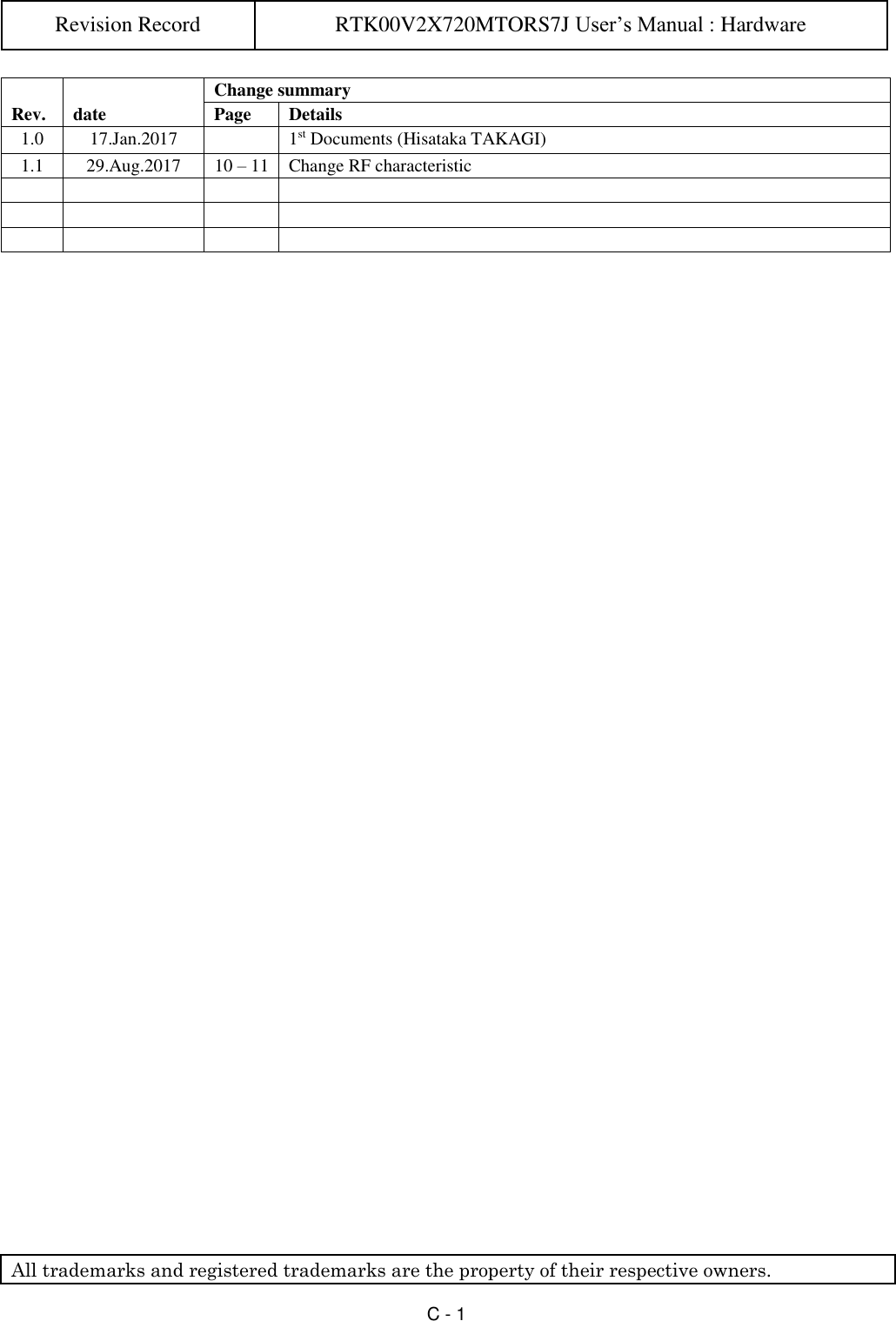
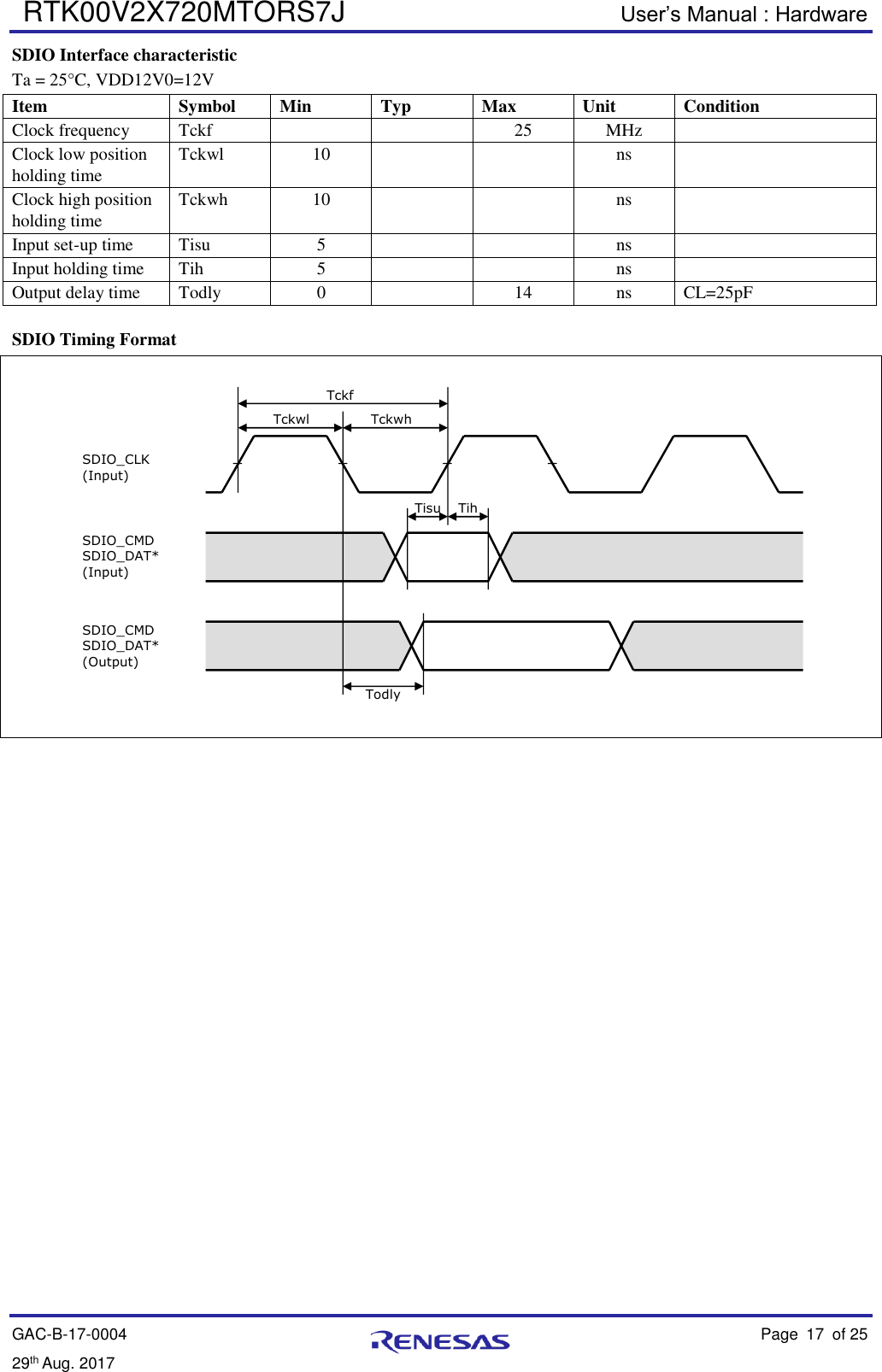
![RTK00V2X720MTORS7J User’s Manual : Hardware GAC-B-17-0004 Page 9 of 25 29th Aug. 2017 3. Function details *VDD1V2 / VDD3V0 / VDD5V0 / VDD12V0 described in this chapter are correspond to symbol described in “2.1 Block diagram”. 3.1 Absolute Maximum Rating Item Symbol Maximum Rate Unit Condition Supply Voltage VDD12V0 -0.3 ~ +43.5 [V] From DC jack VDD5V0 -0.3 ~ +6.0 [V] From Mini PCIE 3.2 Electrical Characteristics Operation Temperature Item Symbol Min Typ Max Unit Condition Operation temperature Ta +25 [°C] Operation Voltage Item Symbol Min Typ Max Unit Condition Supply Voltage VDD12V0 12 [V] From DC jack VDD5V0 4.75 5 5.25 [V] From mini PCIE DC characteristic Ta = 25°C, standalone operation, VDD12V0=12V(AC adapter) Item Symbol Min Typ Max Unit Condition Current consumption (diversity off) VDD12V0 TBD [mA] Listen mode TBD [mA] Rx mode TBD [mA] Tx mode (@24dBm) Current consumption (diversity on) VDD12V0 TBD [mA] Listen mode TBD [mA] Rx mode TBD [mA] Tx mode (@24dBm)](https://usermanual.wiki/Bwave-Technology/W2R.Users-Manual-revised/User-Guide-3665302-Page-9.png)
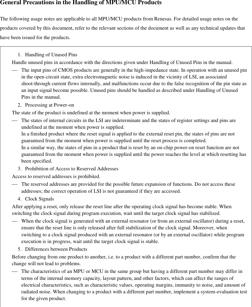
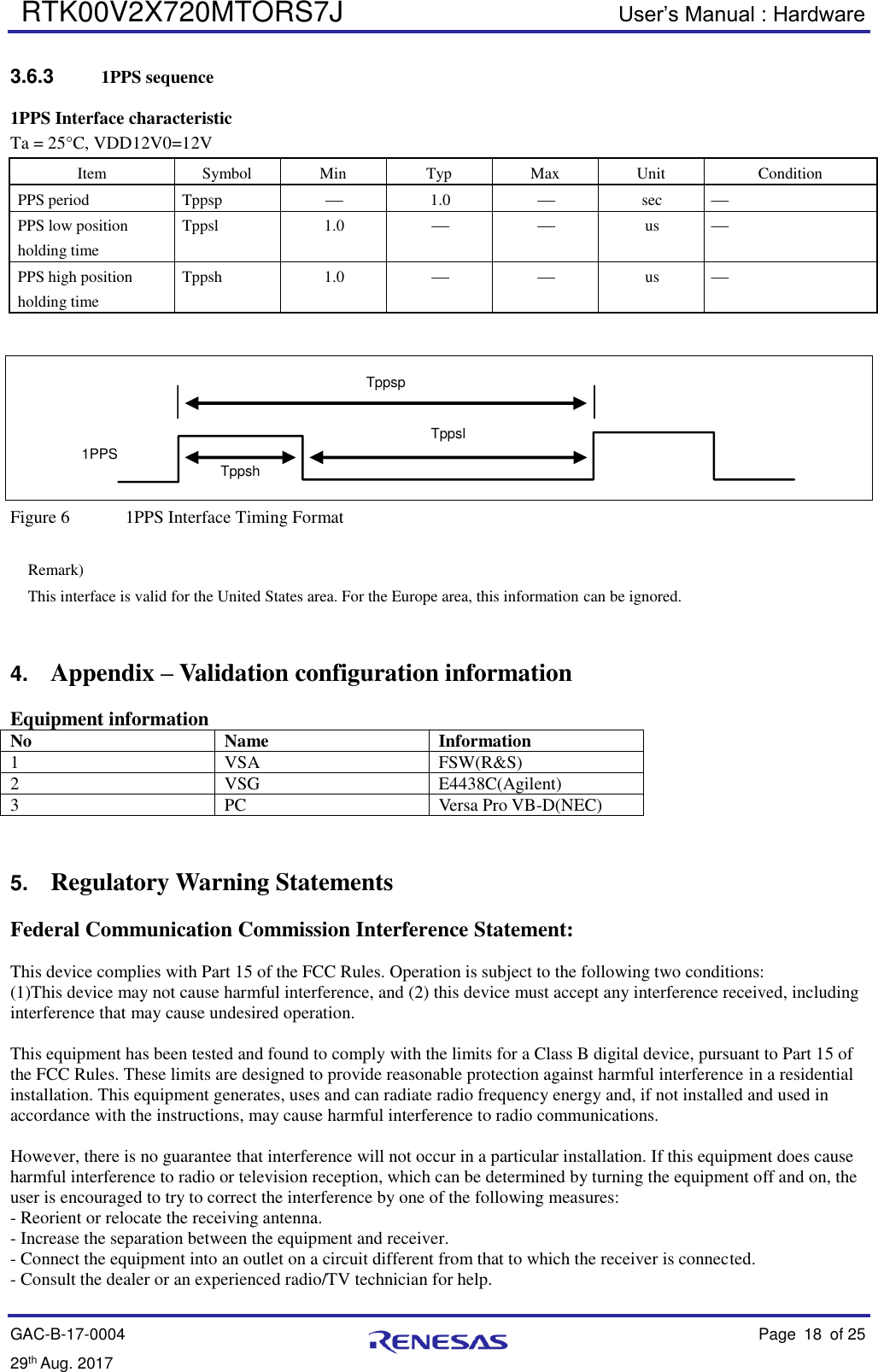
![RTK00V2X720MTORS7J User’s Manual : Hardware GAC-B-17-0004 Page 10 of 25 29th Aug. 2017 3.3 RF characteristic *1 typical operating condition (Just informative, not guaranteed.): *1 HW = Tortuga7, Ta = 25°C, standalone operation, VDD12V0=12V(AC adapter) *1 Measurement point is circled in red in the figure below 3.3.1 Receive characteristic Min Typ Max Unit Condition Frequency range 5850 5925 [MHz] Input VSWR 2.0 - 5890MHz Minimum Sensitivity (Diversity off) -95 [dBm] Data rate = 3Mbps -94 [dBm] Data rate = 6Mbps -88 [dBm] Data rate = 12Mbps -78 [dBm] Data rate = 27Mbps Minimum Sensitivity (Diversity on) -95 [dBm] Data rate = 3Mbps -95 [dBm] Data rate = 6Mbps -90 [dBm] Data rate = 12Mbps -81 [dBm] Data rate = 27Mbps Maximum Input Level (Diversity off) -20 [dBm] Data rate = 27Mbps Maximum Input Level (Diversity on) -20 [dBm] Data rate = 27Mbps Adjacent channel rejection (Diversity off) 29 [dB] Data rate = 3Mbps 29 [dB] Data rate = 6Mbps 27 [dB] Data rate = 12Mbps 23 [dB] Data rate = 27Mbps Nonadjacent Adjacent channel rejection (Diversity off) 43 [dB] Data rate = 3Mbps 40 [dB] Data rate = 6Mbps 36 [dB] Data rate = 12Mbps 27 [dB] Data rate = 27Mbps](https://usermanual.wiki/Bwave-Technology/W2R.Users-Manual-revised/User-Guide-3665302-Page-10.png)
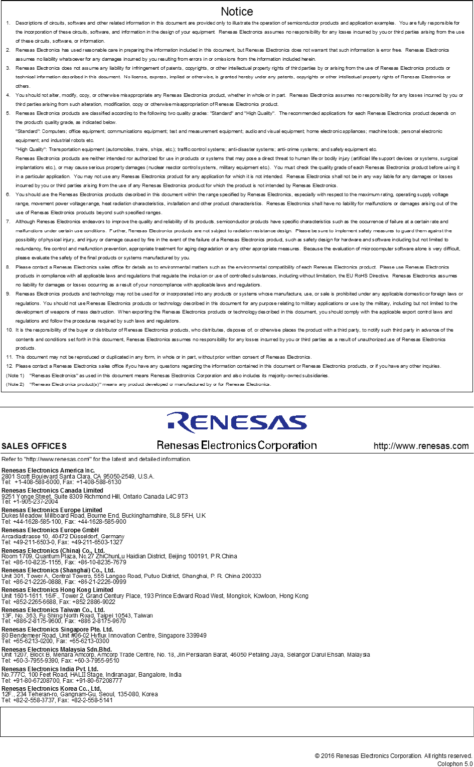
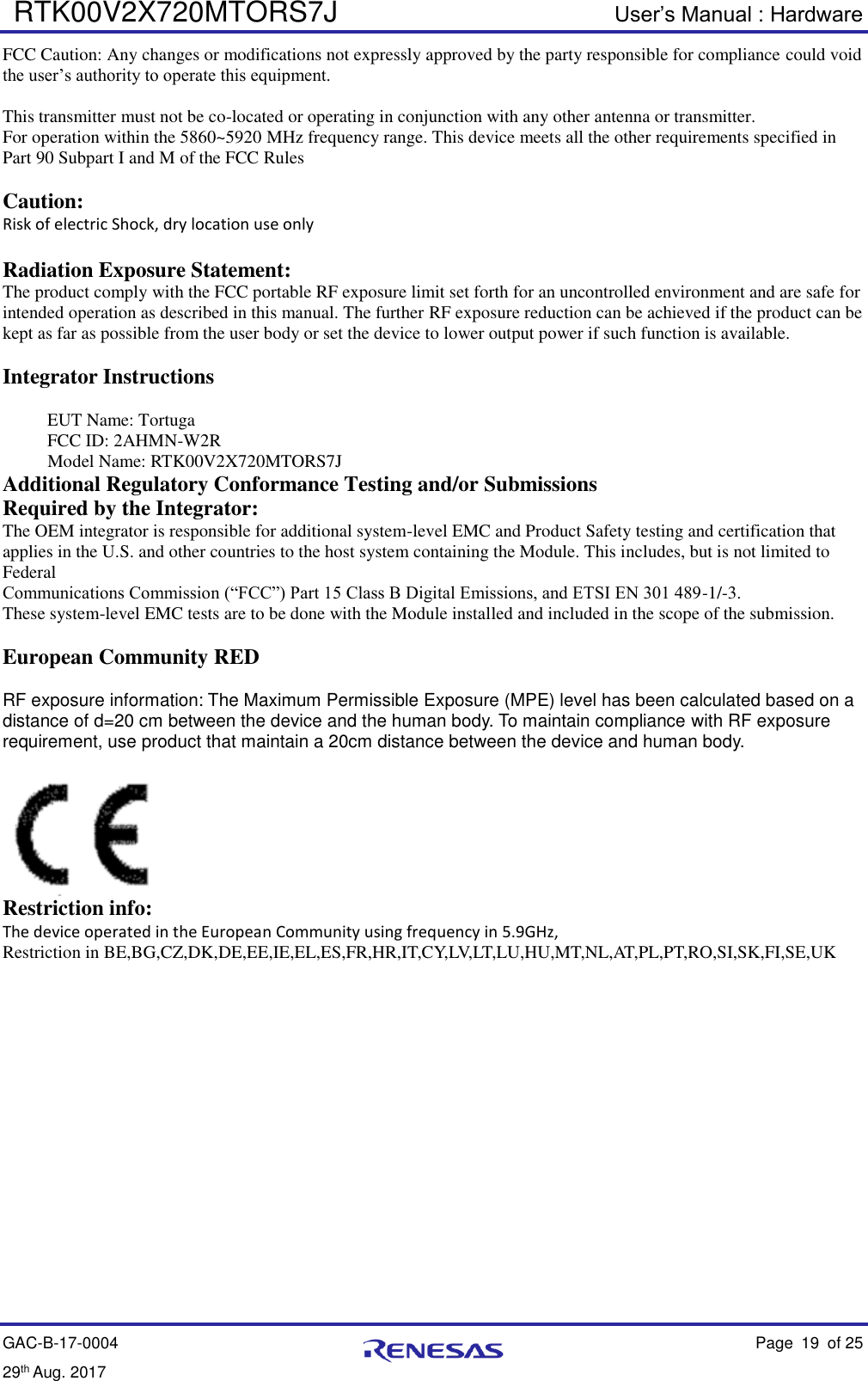
![RTK00V2X720MTORS7J User’s Manual : Hardware GAC-B-17-0004 Page 11 of 25 29th Aug. 2017 3.3.2 Transmit characteristic Min Typ Max Unit Condition Frequency range 5850 5925 [MHz] Output VSWR 24 5890MHz Maximum out put Power(ANT_B) -8 [dBm] 5890MHz Maximum out put Power(ANT_A) -7 [dBm] 5890MHz Minimum out put Power(ANT_B) -35 [dBm] 5890MHz Minimum out put Power(ANT_A) 30 [dBm] 5890MHz Output Power control range 0.5 [dB] 5890MHz Power control step -28 [dB] Relative constellation error -28 [dB] Data rate = 3Mbps -28 Data rate = 6Mbps -28 Data rate = 12Mbps -32 Data rate = 27Mbps Spectrum Mask (in band) -32 [dBr/100KHz] @5890MHz 4.5MHz<f<5.0MHz offset Pout = 24dBm -36 5.0MHz<f<5.5MHz offset Pout =24dBm -54 5.5MHz<f<10.0MHz offset ±5.5MHz Pout= 24dBm 24 10.0MHz<f<15.0MHz offset Pout=24dBm](https://usermanual.wiki/Bwave-Technology/W2R.Users-Manual-revised/User-Guide-3665302-Page-11.png)
![RTK00V2X720MTORS7J User’s Manual : Hardware GAC-B-17-0004 Page 20 of 25 29th Aug. 2017 6. EU Declaration of Conformity (DoC) EU Declaration of Conformity (DoC) Hereby we, Name of manufacturer: Shanghai Bwave Technology Co.,Ltd. Address: 6F, Building 12, 399 Keyuan Road,Zhangjiang Hi-Tech Park Zip code & City: Shanghai Country: China Telephone number: 021-50803833 declare that this DoC is issued under our sole responsibility and that this product: Product description: Tortuga Type designation(s): RTK00V2X720MTORS7J Trademark: RENESAS Batch / Serial number: Object of the declaration (further identification of the radio equipment allowing traceability; it may include a color image for the identification of the radio equipment): [Model: RTK00V2X720MTORS7J] is in conformity with the relevant Union harmonization legislation: Radio Equipment directive: 2014 / 53 / EU and other Union harmonization legislation where applicable: N/A with reference to the following standards applied: EN 60950-1: 2006+A11: 2009+A1: 2010+A12: 2011+A2: 2013; Draft EN 301 489-1 V2.2.0(2017-03); Final Draft EN 301 489-3 V2.1.1(2017-03); EN 302 571 V2.1.1 (2017-02); EN 62311:2008 The Notified Body Telefication B.V., with Notified Body number 0560 performed: [Modules: B] Where applicable: The issued the EU-type examination certificate: [ ] Description of accessories and components, including software, which allow the radio equipment to operate as intended and covered by the DoC: .………………………………………………………………………………………………………… Signed for and on behalf of: Shanghai, Jul. 28, 2017 Changming ZHOU, Manager Place and date of issue Name, Function, signature](https://usermanual.wiki/Bwave-Technology/W2R.Users-Manual-revised/User-Guide-3665302-Page-20.png)