Bwave Technology W2R Tortuga User Manual revised
Shanghai Bwave Technology Co.,Ltd. Tortuga Users Manual revised
Contents
- 1. Users Manual
- 2. Users Manual revised
Users Manual revised
All information contained in these materials, including products and product specifications,
represents information on the product at the time of publication and is subject to change by
Renesas Electronics Corp. without notice. Please review the latest information published by
Renesas Electronics Corp.
RTK00V2X720MTORS7J
User’s Manual: Hardware
Rev.1.1 Aug. 2017
GAC-B-17-0004

RTK00V2X720MTORS7J User’s Manual : Hardware
GAC-B-17-0004 Page
2
of 25
29th Aug. 2017
Introduction
RTK00V2X720MTORS7J(Tortuga) is an evaluation board for RTK00V2X7200MPIN7J (V2X wireless module).
Tortuga can be used as standalone without the need of Host board, and be evaluated RF performance of V2X wireless
module. Tortuga also be used in conjunction with the Host board.
V2X wireless module has optimized function to realize IEEE802.11p PHY layer function. This product conforms not
only to 802.11p standard but 1609.4 and ETSI standard. This module provides cost effective, low power and small form
factor solution for communication unit manufacture.
Overview
Tortuga is an evaluation board for V2X wireless module(including Renesas’ ASSP and suitable component). V2X
wireless module has optimized function to realize ETSI EN 302 571/ ETSI EN 302 663 PHY/MAC layer function. This
product provides cost effective, low power and small form factor solution to communication unit manufacture.
V2X wireless module includes radio transceiver, PA, LNA , antenna switch, Filters and peripherals.
Feature
- Support Standard: ETSI EN 302 571/ ETSI EN 302 663 / IEEE802.11p™ -2010<15.July.2010> PHY/MAC protocol
with Firmware
- Operational Frequency band: 5.9GHz
- Using 32bit CPU core, Operating Frequency: up to 160MHz
- Internal memory: RAM/128kByte, ROM/32kByte, EEPROM/512Byte
- Mini PCIE Connector
- SDIO interface for host CPU
- UART interfaces
- USB interfaces
- Integrate Function for ETSI EN 302 571/ ETSI EN 302 663
OFDM Modulator/ Demodulator with Maximum Ratio Converting diversity
MAC hardware accelerator
- Power Supply: 12V from AC Adapter or 5.0V from Host board
- Peak Power Consumption (at 12 V)
TYP:
- Listen mode : TBD (diversity on)/TBD(diversity off)
- Rx mode : TBD (diversity on)/TBD(diversity off)
- Tx mode : TBD (@24dBm)
- Operating Temperature
Ta = -40 to +85 degree

RTK00V2X720MTORS7J User’s Manual : Hardware
GAC-B-17-0004 Page
3
of 25
29th Aug. 2017
Contents
1. DIMENSION AND LAYOUT ..................................................................................................................4
1.1 BOARD LAYOUT INFORMATION 4
2. BOARD DESCRIPTION ........................................................................................................................6
2.1 BLOCK DIAGRAM 6
2.2 MINI PCIE PIN INFORMATION 7
2.3 POWER SUPPLY 8
2.4 USAGE FOR STANDALONE OPERATION 8
3. FUNCTION DETAILS ...........................................................................................................................9
3.1 ABSOLUTE MAXIMUM RATING 9
3.2 ELECTRICAL CHARACTERISTICS 9
3.3 RF CHARACTERISTIC 10
3.3.1 Receive characteristic
10
3.3.2 Transmit characteristic
11
3.4 MODE TRANSFER DEFINITION AND SUB BOARD CONTROL 12
3.5 POWER UP/DOWN, RESET, WDT SEQUENCE 14
3.5.1 Power On / Off Sequence
14
3.5.2 Reset sequence
15
3.5.3 WDT Reset timing
15
3.6 LOGIC INTERFACE AC CHARACTERISTICS 16
3.6.1 UART sequence
16
3.6.2 SDIO sequence
16
3.6.3 1PPS sequence
18
4. APPENDIX – VALIDATION CONFIGURATION INFORMATION ....................................................... 18
5. REGULATORY WARNING STATEMENTS ......................................................................................... 18
6. EU DECLARATION OF CONFORMITY (DOC) ................................................................................... 20
7. MANUFACTURER INFORMATION .................................................................................................... 21
RTK00V2X720MTORS7J User’s Manual : Hardware
GAC-B-17-0004 Page
4
of 25
29th Aug. 2017
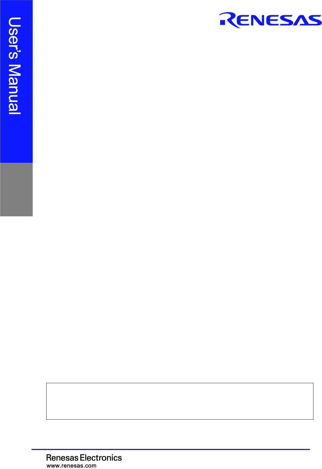
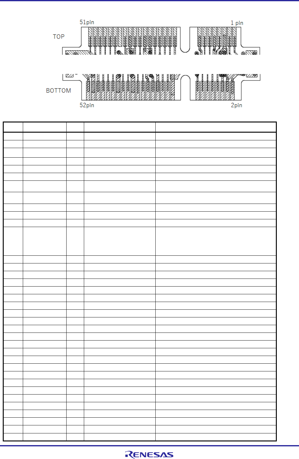
1. Dimension and Layout
1.1 Board layout information
Figure1. Board top view information
Unit: mm
RTK00V2X720MTORS7J User’s Manual : Hardware
GAC-B-17-0004 Page
5
of 25
29th Aug. 2017
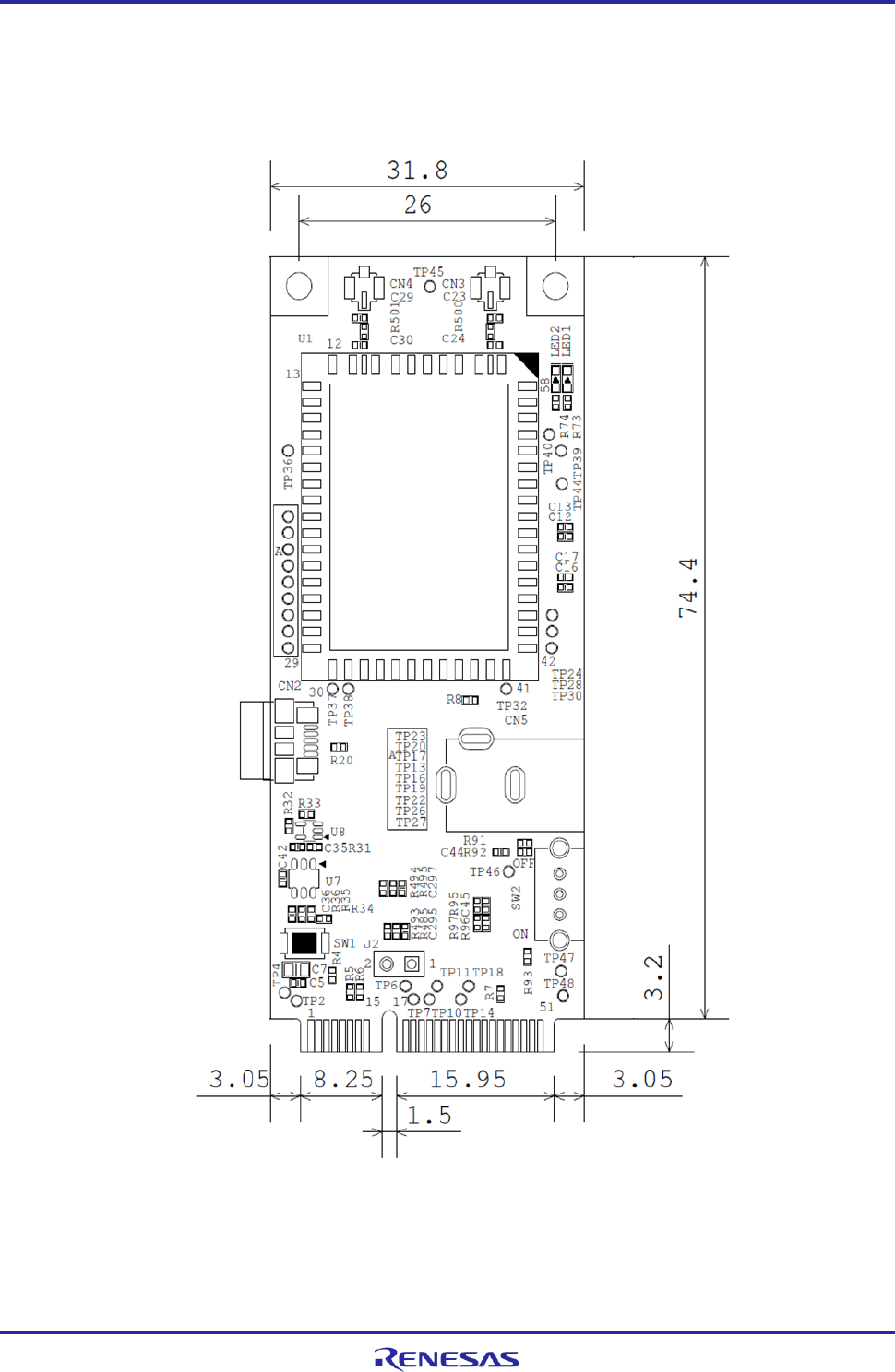
Figure2. Board bottom view information
Unit: mm
RTK00V2X720MTORS7J User’s Manual : Hardware
GAC-B-17-0004 Page
6
of 25
29th Aug. 2017
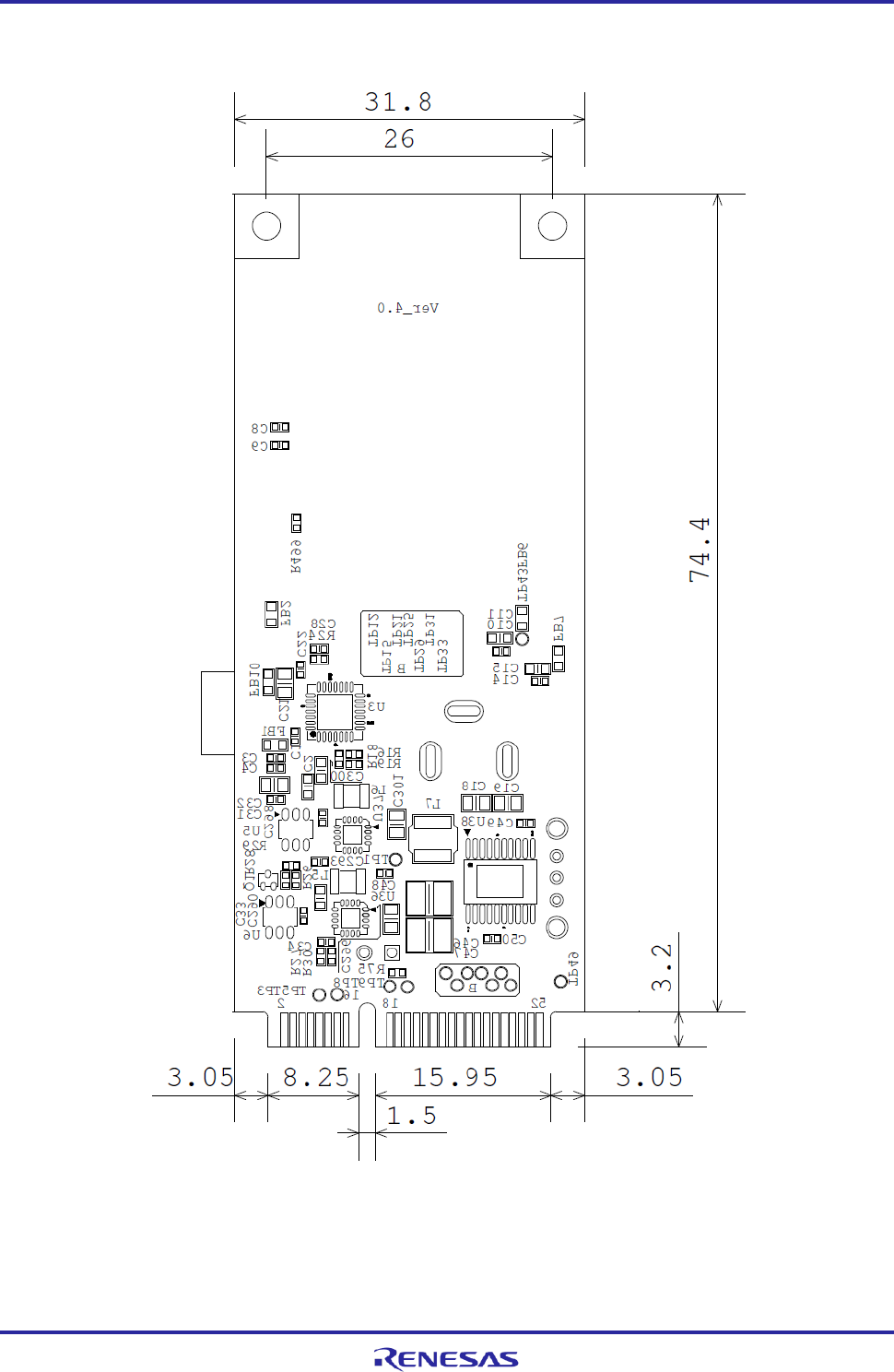
2. Board description
2.1 BLOCK Diagram
RTK00V2X720MTORS7J User’s Manual : Hardware
GAC-B-17-0004 Page
7
of 25
29th Aug. 2017
2.2 Mini PCIE pin information
Pin
Pin Name
I/O
Functional
Description
1
RESERVE
I/O
-
No connection(only connected to test pin)
2
RESERVE
I/O
-
No connection
3
RESERVE
I/O
-
No connection(only connected to test pin)
4
GND
-
GND
GND
5
5.0V
-
Voltage Supply
5V voltage supply
6
5.0V
-
Voltage Supply
5V voltage supply
7
RESET
I
CMOS Schmitt Trigger Input
(with Pull-Up)
System reset input (Low Active)
8
1PPS
I
CMOS Schmitt Trigger I
(with Pull-Down)
If you don’t use, select open.
9
GND
-
GND
GND
10
RESERVE
I/O
-
No connection(only connected to test pin)
11
UART0_TXD
O
CMOS Output
UART0 Tx signal [TXD]
12
ANT_M
I
CMOS Schmitt Trigger I
(with Pull-Up)
RX Diversity Enable selects.
- High : Diversity
- Low : Single_ANT B
If you don’t use, select open.
13
UART0_RXD
I
CMOS Schmitt Trigger Input
UART0 Rx signal [RXD]
14
RESERVE
I/O
-
No connection(only connected to test pin)
15
GND
-
GND
GND
16
STATE
O
CMOS Output
Status indication signal
17
RESERVE
I/O
-
No connection(only connected to test pin)
18
GND
-
GND
GND
19
RESERVE
I/O
-
No connection(only connected to test pin)
20
RESERVE
I/O
-
No connection(only connected to test pin)
21
GND
-
GND
GND
22
RESERVE
I/O
-
No connection(only connected to test pin)
23
RESERVE
I/O
-
No connection(only connected to test pin)
24
5.0V
-
Voltage Supply
5V voltage supply
25
RESERVE
I/O
-
No connection(only connected to test pin)
26
GND
-
GND
GND
27
GND
-
GND
GND
28
5.0V
-
Voltage Supply
5V voltage supply
29
GND
-
GND
GND
30
RESERVE
I/O
-
No connection(only connected to test pin)
31
RESERVE
I/O
-
No connection(only connected to test pin)
32
RESERVE
I/O
-
No connection(only connected to test pin)
33
RESERVE
I/O
-
No connection(only connected to test pin)
34
GND
-
GND
GND
35
GND
-
GND
GND
36
RESERVE
I/O
-
No connection(only connected to test pin)

RTK00V2X720MTORS7J User’s Manual : Hardware
GAC-B-17-0004 Page
8
of 25
29th Aug. 2017
Pin
Pin Name
I/O
Functional
Description
37
SDIO_CLK
I
CMOS Schmitt Trigger Input
(with Pull-Up)
SDIO clock [CLK]
38
RESERVE
I/O
-
No connection(only connected to test pin)
39
RESERVE
I/O
-
No connection(only connected to test pin)
40
GND
-
GND
GND
41
GND
-
GND
GND(Pull Down
42
RESERVE
I/O
-
No connection(only connected to test pin)
43
SDIO_DAT3
I/O
CMOS I/O with Pull-Up
SDIO data [DAT3]
44
RESERVE
I/O
-
No connection(only connected to test pin)
45
SDIO_DAT2
I/O
CMOS I/O with Pull-Up
SDIO data [DAT2]
46
RESERVE
I/O
-
No connection(only connected to test pin)
47
SDIO_DAT1
I/O
CMOS I/O with Pull-Up
SDIO data [DAT1]
48
5.0V
-
Voltage Supply
5V voltage supply
49
SDIO_DAT0
I/O
CMOS I/O with Pull-Up
SDIO data [DAT0]
50
GND
-
GND
GND
51
SDIO_CMD
I/O
CMOS I/O with Pull-Up
SDIO command [CMD]
52
RESERVE
I/O
-
No connection
2.3 Power Supply
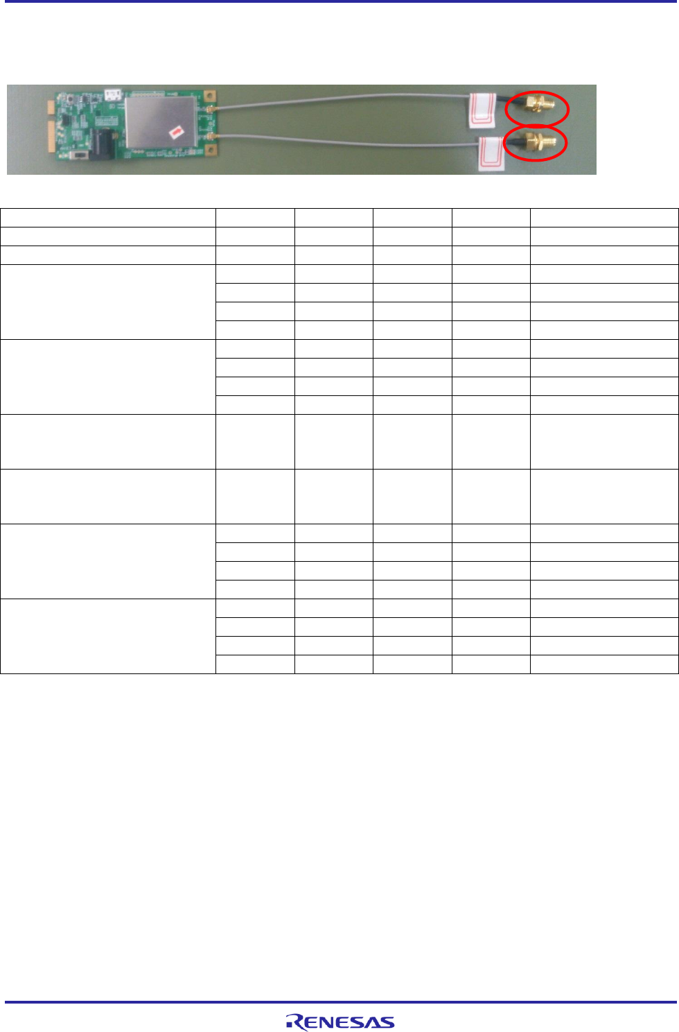
Tortuga are powered from the HOST board if used in conjunction with the HOST board.
For standalone operation Tortuga are powered from the AC adapter(12V/2A).
2.4 Usage for standalone operation
Please refer to the “UW2b Tortuga test TP quick manual“ for usage of standalone operation.
RTK00V2X720MTORS7J User’s Manual : Hardware
GAC-B-17-0004 Page
9
of 25
29th Aug. 2017
3. Function details
*VDD1V2 / VDD3V0 / VDD5V0 / VDD12V0 described in this chapter are correspond to symbol described in “2.1
Block diagram”.
3.1 Absolute Maximum Rating
Item
Symbol
Maximum Rate
Unit
Condition
Supply Voltage
VDD12V0
-0.3 ~ +43.5
[V]
From DC jack
VDD5V0
-0.3 ~ +6.0
[V]
From Mini PCIE
3.2 Electrical Characteristics
Operation Temperature
Item
Symbol
Min
Typ
Max
Unit
Condition
Operation
temperature
Ta
+25
[°C]
Operation Voltage
Item
Symbol
Min
Typ
Max
Unit
Condition
Supply Voltage
VDD12V0
12
[V]
From DC jack
VDD5V0
4.75
5
5.25
[V]
From mini PCIE
DC characteristic
Ta = 25°C, standalone operation, VDD12V0=12V(AC adapter)
Item
Symbol
Min
Typ
Max
Unit
Condition
Current
consumption
(diversity off)
VDD12V0
TBD
[mA]
Listen mode
TBD
[mA]
Rx mode
TBD
[mA]
Tx mode (@24dBm)
Current
consumption
(diversity on)
VDD12V0
TBD
[mA]
Listen mode
TBD
[mA]
Rx mode
TBD
[mA]
Tx mode (@24dBm)
RTK00V2X720MTORS7J User’s Manual : Hardware
GAC-B-17-0004 Page
10
of 25
29th Aug. 2017
3.3 RF characteristic
*1 typical operating condition (Just informative, not guaranteed.):
*1 HW = Tortuga7, Ta = 25°C, standalone operation, VDD12V0=12V(AC adapter)
*1 Measurement point is circled in red in the figure below
3.3.1 Receive characteristic
Min
Typ
Max
Unit
Condition
Frequency range
5850
5925
[MHz]
Input VSWR
2.0
-
5890MHz
Minimum Sensitivity
(Diversity off)
-95
[dBm]
Data rate = 3Mbps
-94
[dBm]
Data rate = 6Mbps
-88
[dBm]
Data rate = 12Mbps
-78
[dBm]
Data rate = 27Mbps
Minimum Sensitivity
(Diversity on)
-95
[dBm]
Data rate = 3Mbps
-95
[dBm]
Data rate = 6Mbps
-90
[dBm]
Data rate = 12Mbps
-81
[dBm]
Data rate = 27Mbps
Maximum
Input Level
(Diversity off)
-20
[dBm]
Data rate = 27Mbps
Maximum
Input Level
(Diversity on)
-20
[dBm]
Data rate = 27Mbps
Adjacent channel rejection
(Diversity off)
29
[dB]
Data rate = 3Mbps
29
[dB]
Data rate = 6Mbps
27
[dB]
Data rate = 12Mbps
23
[dB]
Data rate = 27Mbps
Nonadjacent Adjacent channel
rejection
(Diversity off)
43
[dB]
Data rate = 3Mbps
40
[dB]
Data rate = 6Mbps
36
[dB]
Data rate = 12Mbps
27
[dB]
Data rate = 27Mbps

RTK00V2X720MTORS7J User’s Manual : Hardware
GAC-B-17-0004 Page
11
of 25
29th Aug. 2017
3.3.2 Transmit characteristic
Min
Typ
Max
Unit
Condition
Frequency range
5850
5925
[MHz]
Output VSWR
24
5890MHz
Maximum out put Power(ANT_B)
-8
[dBm]
5890MHz
Maximum out put Power(ANT_A)
-7
[dBm]
5890MHz
Minimum out put Power(ANT_B)
-35
[dBm]
5890MHz
Minimum out put Power(ANT_A)
30
[dBm]
5890MHz
Output Power control range
0.5
[dB]
5890MHz
Power control step
-28
[dB]
Relative constellation error
-28
[dB]
Data rate = 3Mbps
-28
Data rate = 6Mbps
-28
Data rate = 12Mbps
-32
Data rate = 27Mbps
Spectrum Mask
(in band)
-32
[dBr/100
KHz]
@5890M
Hz
4.5MHz<f<5.0MHz offset Pout
= 24dBm
-36
5.0MHz<f<5.5MHz offset
Pout =24dBm
-54
5.5MHz<f<10.0MHz offset
±5.5MHz Pout=
24dBm
24
10.0MHz<f<15.0MHz offset
Pout=24dBm
RTK00V2X720MTORS7J User’s Manual : Hardware
GAC-B-17-0004 Page
12
of 25
29th Aug. 2017
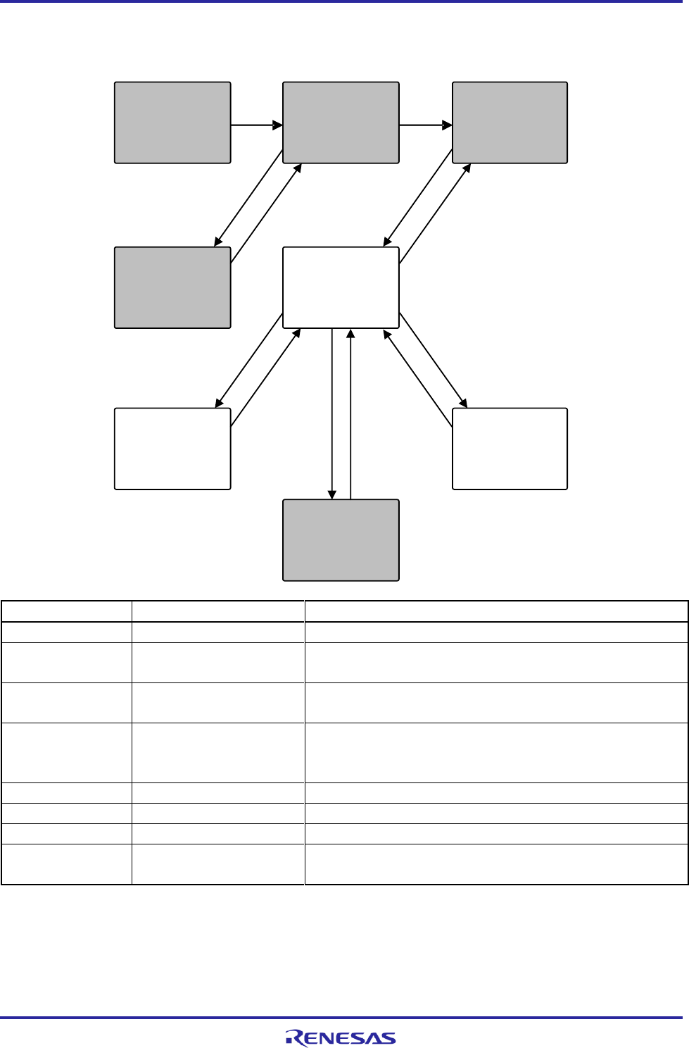
3.4 Mode Transfer Definition and sub board control
Mode
State
Note
Reset
Reset assert.
Transfer from the mode to the Reset mode by reset signal
INIT
Initialize RF block, internal
register and other function.
Initialized LSI function after booting firmware
IDLE
Waiting start request from Host
CPU
Listen
Waiting the packet indication.
Transfer the Receive mode by detecting the receive signal power, or
transfer the Transmit mode by internal transmit request, or transfer the
IDLE mode by stop request from Host CPU
Receive
Receive signal processing.
Transmit
Transmit signal processing.
Frequency Change
Changing Tx/Rx frequency.
TEST
Test mode.
Operate loop back calibration and other test for performance
optimization
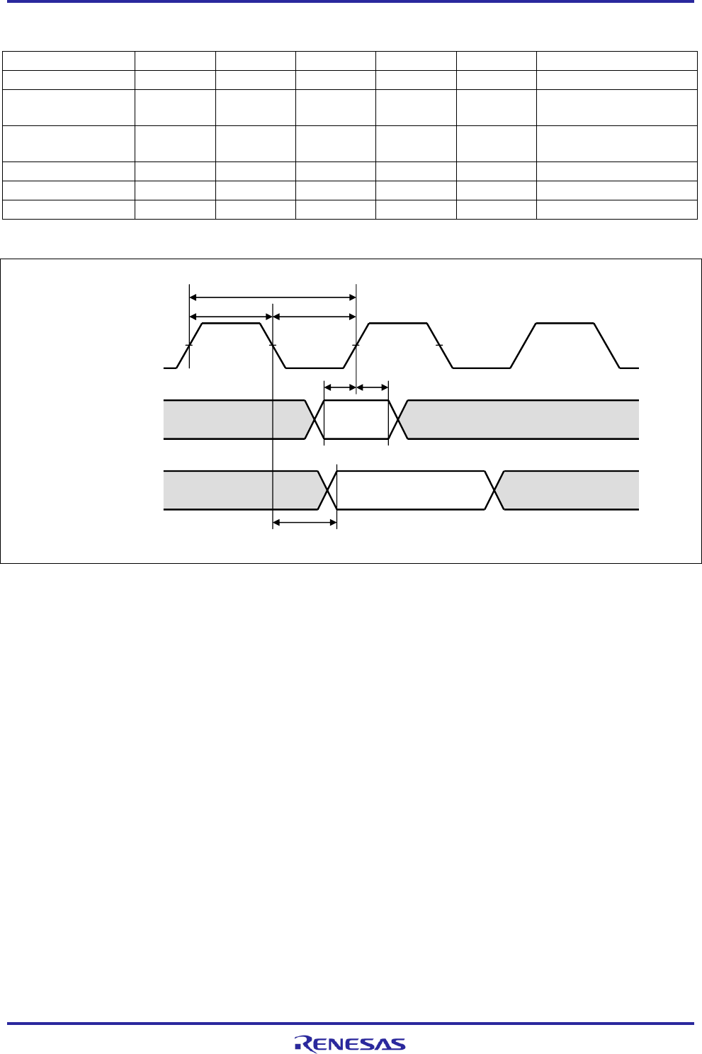
The MAC firmware and BBWLAN control the external RF circuits via the control pins ANT_SW_P, ANT_SW_N,
Reset INIT
Receive
IDLE
Transmit
Listen
Initialization
Complete
Reset
De- assertion
TEST
Frequency
Change Request
Frequency
Change
Start TEST
Finish TEST
Frequency
Change Complete
Start Request
(from Host CPU)
Stop Request
(from Host CPU)
Packet (Energy)
Detection
Receive
Complete
Transmission
Request
Transmission
Complete
RTK00V2X720MTORS7J User’s Manual : Hardware
GAC-B-17-0004 Page
13
of 25
29th Aug. 2017
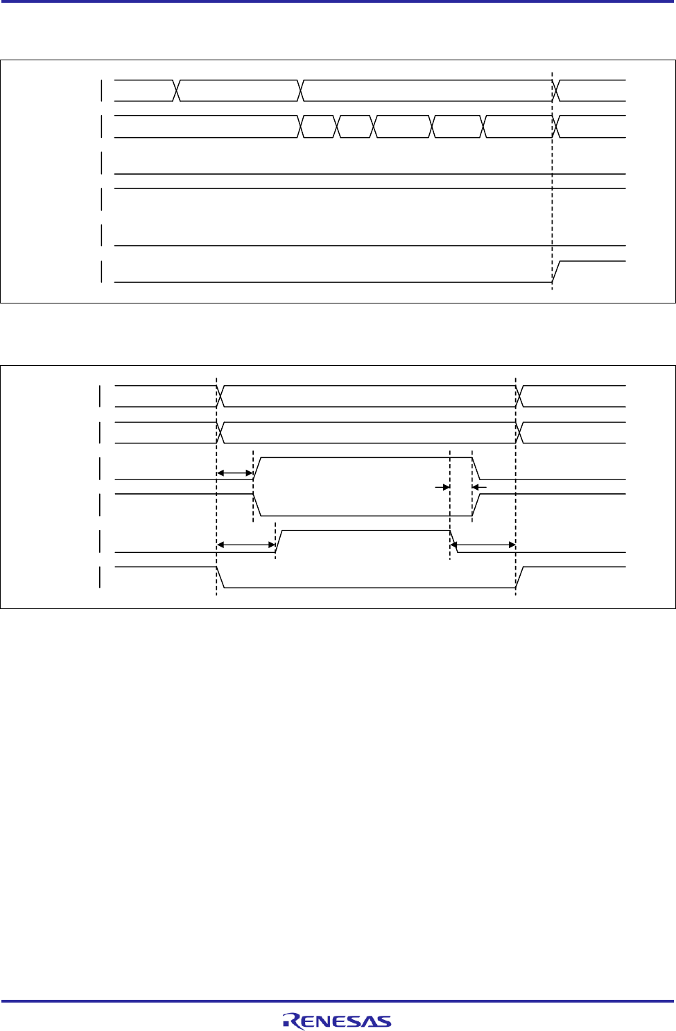
PAEN(Pin name = PAPE) and RFCNTL. The operation of these external RF circuit control pins according to the internal
transceiver state and/or operation inside RF block are summarized in Fig. 3 and Fig. 4.
Figure 3 Operation of the External RF Circuit Control Pins (Reset and Initialization)
Figure 4 Operation of the External RF Circuit Control Pins (Transmission and Listening)
Remarks)
*1) The assertion timings of ANT_SW_P/N and PAEN1 can be tuned from 0 to 12.7us independently.
*2) RFCNTL2, PAEN2, ANT_M pins are reserved for the future as an optional function which might be realized by the
MAC firmware. The detail operations are not defined in this hardware document.
RX
ListenReset
Idle Idle Calibration Warm-up
ANT_SW_P
ANT_SW_N
PAEN1
RFCNTL1
‘Low’
‘High’
‘Low’
‘Low’
Operation
Inside RF
Transceiver
state INIT
(CPU Initialization) INIT
(RF/PHY Initialization)
RF
Reset Register
Program
RX
ListenTransmit
RX TX
ANT_SW_P
ANT_SW_N
PAEN1
RFCNTL1
‘Low’
‘High’
Listen
‘High’
‘Low’
0 to 12.7 us
0 to 12.7 us 0 to 12.7 us
0 or 1 or 2 us
Transceiver
state
Operation
Inside RF
RTK00V2X720MTORS7J User’s Manual : Hardware
GAC-B-17-0004 Page
14
of 25
29th Aug. 2017
3.5 Power up/down, Reset, WDT sequence
3.5.1 Power On / Off Sequence
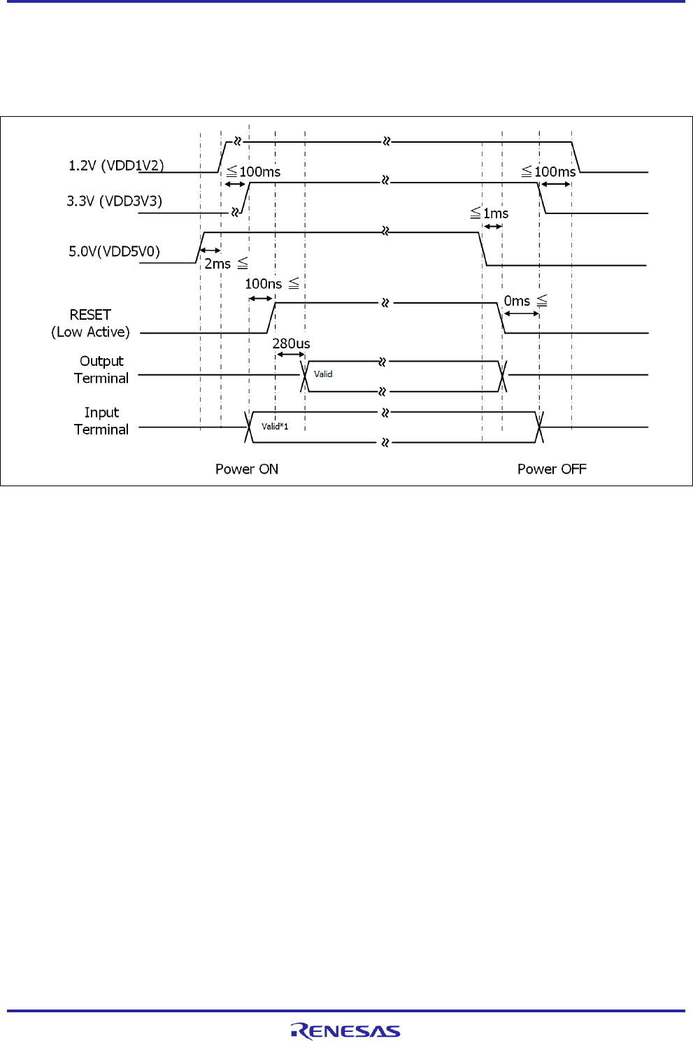
Figure 5 Operation of the External RF Circuit Control Pins (Transmission and Listening)
*1 “Valid” to module input pin in the figure means drive valid data (or pull-up/down) from external.
*2 each input signal level to Input from external shall not exceed VDD+0.3V (VDD3V3, VDD1V2,VDD5V0)
correspondingly. .
*3 until 280us after reset release, output pin is not defined. After that, it drives initial value for each pin.
For power supply on, apply power in the order, 5.0V , 1.2V , 3.3V, and after passed more than 100ns of Low level,
RESET is released. In order to PLL reset and to stabilize PLL oscillation, after about 280us, clock is supplied to LSI.
For power off, the reverse order shall be done, i.e. RESET is “Active”, and switch off 5.0V , 3.3 V and 1.2 V.
RTK00V2X720MTORS7J User’s Manual : Hardware
GAC-B-17-0004 Page
15
of 25
29th Aug. 2017
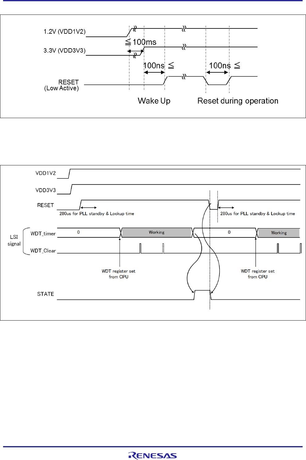
3.5.2 Reset sequence
With making RESET pin ”Low”, LSI reset is executed. To be surely reset, hold RESETB level ”Low” for minimum
100ns. Also for reset under operation, control RESET level ”Low” for minimum 100ns.
3.5.3 WDT Reset timing
When Watch-dog time (WDT) counter becomes overflow, STATE signal output “High”, and informs WDT flow over to
host CPU software. Then LSI stops as reset status. Host CPU software is able to re-start LSI with external RESET
signal.
RTK00V2X720MTORS7J User’s Manual : Hardware
GAC-B-17-0004 Page
16
of 25
29th Aug. 2017
3.6 Logic interface AC Characteristics
3.6.1 UART sequence
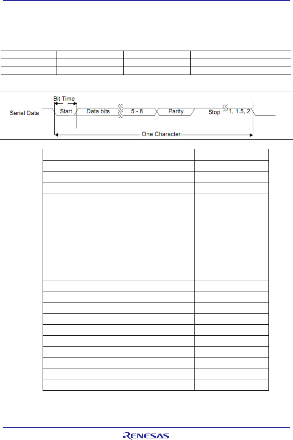
UART Interface characteristic
Ta = 25°C, VDD12V0
Item
Symbol
Min
Typ
Max
Unit
Condition
Baud rate
fUTRXD
50
128000
bps
Bit Time
tUTRXD
7.81
20000
us
tUTRXD=1/fUTRXD
UART Serial Data Format
Baud Rate (bps)
Hex Divisor Setting
Bit Time (us)
50
0x61A8
20000.00
75
0x411B
13333.33
110
0x2C64
9090.91
134.5
0x244E
7434.94
150
0x208D
6666.67
300
0x1047
3333.33
600
0x0823
1666.67
1200
0x0412
833.33
1800
0x02B6
555.56
2000
0x0271
500.00
2400
0x0209
416.67
3600
0x015B
277.78
4800
0x0104
208.33
7200
0x00AE
138.89
9600
0x0082
104.17
19200
0x0041
52.08
38400
0x0021
26.04
56000
0x0016
17.86
57600
0x0016
17.36
115200
0x000B
8.68
128000
0x000A
7.81
3.6.2 SDIO sequence
RTK00V2X720MTORS7J User’s Manual : Hardware
GAC-B-17-0004 Page
17
of 25
29th Aug. 2017
SDIO Interface characteristic
Ta = 25°C, VDD12V0=12V
Item
Symbol
Min
Typ
Max
Unit
Condition
Clock frequency
Tckf
25
MHz
Clock low position
holding time
Tckwl
10
ns
Clock high position
holding time
Tckwh
10
ns
Input set-up time
Tisu
5
ns
Input holding time
Tih
5
ns
Output delay time
Todly
0
14
ns
CL=25pF
SDIO Timing Format
Tckf
Tckwl Tckwh
Tisu
Todly
SDIO_CLK
SDIO_CMD
SDIO_DAT*
(Input)
(Input)
SDIO_CMD
SDIO_DAT*
(Output)
Tih
RTK00V2X720MTORS7J User’s Manual : Hardware
GAC-B-17-0004 Page
18
of 25
29th Aug. 2017
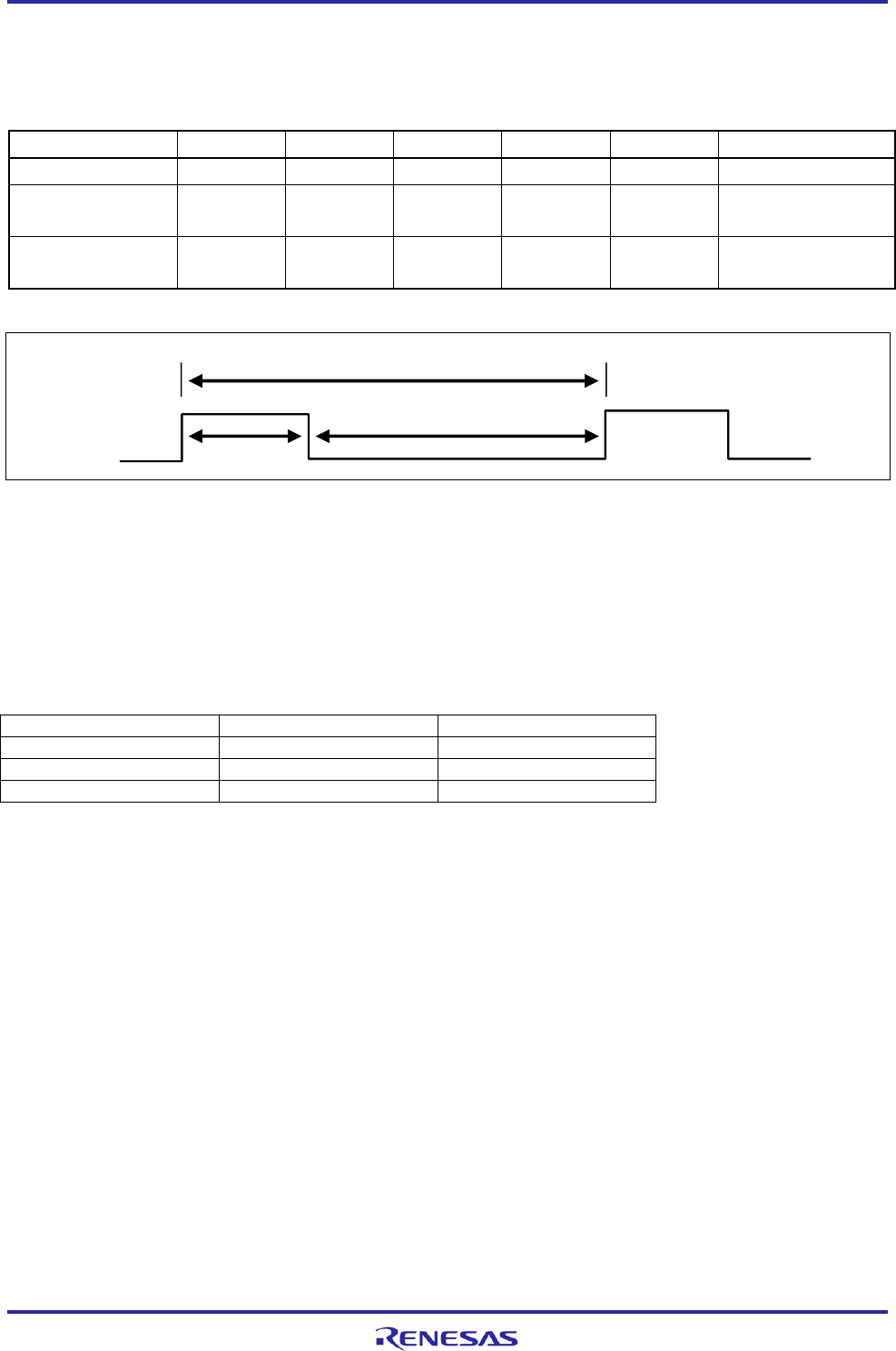
3.6.3 1PPS sequence
1PPS Interface characteristic
Ta = 25°C, VDD12V0=12V
Item
Symbol
Min
Typ
Max
Unit
Condition
PPS period
Tppsp
1.0
sec
PPS low position
holding time
Tppsl
1.0
us
PPS high position
holding time
Tppsh
1.0
us
Figure 6 1PPS Interface Timing Format
Remark)
This interface is valid for the United States area. For the Europe area, this information can be ignored.
4. Appendix – Validation configuration information
Equipment information
No
Name
Information
1
VSA
FSW(R&S)
2
VSG
E4438C(Agilent)
3
PC
Versa Pro VB-D(NEC)
5. Regulatory Warning Statements
Federal Communication Commission Interference Statement:
This device complies with Part 15 of the FCC Rules. Operation is subject to the following two conditions:
(1)This device may not cause harmful interference, and (2) this device must accept any interference received, including
interference that may cause undesired operation.
This equipment has been tested and found to comply with the limits for a Class B digital device, pursuant to Part 15 of
the FCC Rules. These limits are designed to provide reasonable protection against harmful interference in a residential
installation. This equipment generates, uses and can radiate radio frequency energy and, if not installed and used in
accordance with the instructions, may cause harmful interference to radio communications.
However, there is no guarantee that interference will not occur in a particular installation. If this equipment does cause
harmful interference to radio or television reception, which can be determined by turning the equipment off and on, the
user is encouraged to try to correct the interference by one of the following measures:
- Reorient or relocate the receiving antenna.
- Increase the separation between the equipment and receiver.
- Connect the equipment into an outlet on a circuit different from that to which the receiver is connected.
- Consult the dealer or an experienced radio/TV technician for help.
Tppsp
Tppsh
Tppsl
1PPS

RTK00V2X720MTORS7J User’s Manual : Hardware
GAC-B-17-0004 Page
19
of 25
29th Aug. 2017
FCC Caution: Any changes or modifications not expressly approved by the party responsible for compliance could void
the user’s authority to operate this equipment.
This transmitter must not be co-located or operating in conjunction with any other antenna or transmitter.
For operation within the 5860~5920 MHz frequency range. This device meets all the other requirements specified in
Part 90 Subpart I and M of the FCC Rules
Caution:
Risk of electric Shock, dry location use only
Radiation Exposure Statement:
The product comply with the FCC portable RF exposure limit set forth for an uncontrolled environment and are safe for
intended operation as described in this manual. The further RF exposure reduction can be achieved if the product can be
kept as far as possible from the user body or set the device to lower output power if such function is available.
Integrator Instructions
EUT Name: Tortuga
FCC ID: 2AHMN-W2R
Model Name: RTK00V2X720MTORS7J
Additional Regulatory Conformance Testing and/or Submissions
Required by the Integrator:
The OEM integrator is responsible for additional system-level EMC and Product Safety testing and certification that
applies in the U.S. and other countries to the host system containing the Module. This includes, but is not limited to
Federal
Communications Commission (“FCC”) Part 15 Class B Digital Emissions, and ETSI EN 301 489-1/-3.
These system-level EMC tests are to be done with the Module installed and included in the scope of the submission.
European Community RED
RF exposure information: The Maximum Permissible Exposure (MPE) level has been calculated based on a
distance of d=20 cm between the device and the human body. To maintain compliance with RF exposure
requirement, use product that maintain a 20cm distance between the device and human body.
Restriction info:
The device operated in the European Community using frequency in 5.9GHz,
Restriction in BE,BG,CZ,DK,DE,EE,IE,EL,ES,FR,HR,IT,CY,LV,LT,LU,HU,MT,NL,AT,PL,PT,RO,SI,SK,FI,SE,UK

RTK00V2X720MTORS7J User’s Manual : Hardware
GAC-B-17-0004 Page
20
of 25
29th Aug. 2017
6. EU Declaration of Conformity (DoC)
EU Declaration of Conformity (DoC)
Hereby we,
Name of manufacturer:
Shanghai Bwave Technology Co.,Ltd.
Address:
6F, Building 12, 399 Keyuan Road,Zhangjiang Hi-Tech Park
Zip code & City:
Shanghai
Country:
China
Telephone number:
021-50803833
declare that this DoC is issued under our sole responsibility and that this product:
Product description:
Tortuga
Type designation(s):
RTK00V2X720MTORS7J
Trademark:
RENESAS
Batch / Serial number:
Object of the declaration (further identification of the radio equipment allowing traceability; it may include a color image
for the identification of the radio equipment):
[Model: RTK00V2X720MTORS7J]
is in conformity with the relevant Union harmonization legislation:
Radio Equipment directive: 2014 / 53 / EU
and other Union harmonization legislation where applicable:
N/A
with reference to the following standards applied:
EN 60950-1: 2006+A11: 2009+A1: 2010+A12: 2011+A2: 2013;
Draft EN 301 489-1 V2.2.0(2017-03); Final Draft EN 301 489-3 V2.1.1(2017-03);
EN 302 571 V2.1.1 (2017-02);
EN 62311:2008
The Notified Body Telefication B.V., with Notified Body number 0560 performed:
[Modules: B]
Where applicable:
The issued the EU-type examination certificate: [ ]
Description of accessories and components, including software, which allow the radio equipment to operate as intended
and covered by the DoC:
.…………………………………………………………………………………………………………
Signed for and on behalf of:
Shanghai, Jul. 28, 2017 Changming ZHOU, Manager
Place and date of issue Name, Function, signature

RTK00V2X720MTORS7J User’s Manual : Hardware
GAC-B-17-0004 Page
21
of 25
29th Aug. 2017
7. Manufacturer Information
Manufacturer : Shanghai Bwave Technology Co.,Ltd.
Address : 6F, Building 12, 399 Keyuan Road,Zhangjiang Hi-Tech Park
City : Shanghai
Country : China
ORIGINAL EQUIPMENT MANUFACTURER (OEM) NOTES
The OEM must certify the final end product to comply with unintentional radiators (FCC Sections 15.107 and
15.109) before declaring compliance of the final product to Part 15 of the FCC rules and regulations. Integration
into devices that are directly or indirectly connected to AC lines must add with Class II Permissive Change.
The OEM must comply with the FCC labeling requirements. If the module’s label is not visible when installed,
then an additional permanent label must be applied on the outside of the finished product which states: “Contains
transmitter module FCC ID: 2AHMN W2R. Additionally, the following statement should be included on the label
and in the final product’s user manual: “This device complies with Part 15 of the FCC Rules. Operation is subject
to the following two conditions: (1) This device may not cause harmful interferences, and (2) this device must
accept any interference received, including interference that may cause undesired operation.”
The module is limited to installation in mobile or fixed applications. Separate approval is required for all other
operating configurations, including portable configuration with respect to Part 2.1093 and different antenna
configurations
A module or modules can only be used without additional authorizations if they have been tested and granted
under the same intended end‐use operational conditions, including simultaneous transmission operations. When
they have not been tested and granted in this manner, additional testing and/or FCC application filing may be
required. The most straightforward approach to address additional testing conditions is to have the grantee
responsible for the certification of at least one of the modules submit a permissive change application. When
having a module grantee file a permissive change is not practical or feasible, the following guidance provides
some additional options for host manufacturers. Integrations using modules where additional testing and/or FCC
application filing(s) may be required are: (A) a module used in devices requiring additional RF exposure
compliance information (e.g., MPE evaluation or SAR testing); (B) limited and/or split modules not meeting all of
the module requirements; and (C) simultaneous transmissions for independent collocated transmitters not
previously granted together.
This Module is full modular approval, it is limited to OEM installation ONLY.
Integration into devices that are directly or indirectly connected to AC lines must add with Class II Permissive Change.
(OEM) Integrator has to assure compliance of the entire end product incluld the integrated Module.
Additional measurements (15B) and/or equipment authorizations (e.g Verification) may need to be addressed depending
on co-location or simultaneous transmission issues if applicable.
(OEM) Integrator is reminded to assure that these installation instructions will not be made available to the end user of
the final host device.

All trademarks and registered trademarks are the property of their respective owners.
C - 1
Revision Record
RTK00V2X720MTORS7J User’s Manual : Hardware
Rev.
date
Change summary
Page
Details
1.0
17.Jan.2017
1st Documents (Hisataka TAKAGI)
1.1
29.Aug.2017
10 – 11
Change RF characteristic

General Precautions in the Handling of MPU/MCU Products
The following usage notes are applicable to all MPU/MCU products from Renesas. For detailed usage notes on the
products covered by this document, refer to the relevant sections of the document as well as any technical updates that
have been issued for the products.
1. Handling of Unused Pins
Handle unused pins in accordance with the directions given under Handling of Unused Pins in the manual.
The input pins of CMOS products are generally in the high-impedance state. In operation with an unused pin
in the open-circuit state, extra electromagnetic noise is induced in the vicinity of LSI, an associated
shoot-through current flows internally, and malfunctions occur due to the false recognition of the pin state as
an input signal become possible. Unused pins should be handled as described under Handling of Unused
Pins in the manual.
2. Processing at Power-on
The state of the product is undefined at the moment when power is supplied.
The states of internal circuits in the LSI are indeterminate and the states of register settings and pins are
undefined at the moment when power is supplied.
In a finished product where the reset signal is applied to the external reset pin, the states of pins are not
guaranteed from the moment when power is supplied until the reset process is completed.
In a similar way, the states of pins in a product that is reset by an on-chip power-on reset function are not
guaranteed from the moment when power is supplied until the power reaches the level at which resetting has
been specified.
3. Prohibition of Access to Reserved Addresses
Access to reserved addresses is prohibited.
The reserved addresses are provided for the possible future expansion of functions. Do not access these
addresses; the correct operation of LSI is not guaranteed if they are accessed.
4. Clock Signals
After applying a reset, only release the reset line after the operating clock signal has become stable. When
switching the clock signal during program execution, wait until the target clock signal has stabilized.
When the clock signal is generated with an external resonator (or from an external oscillator) during a reset,
ensure that the reset line is only released after full stabilization of the clock signal. Moreover, when
switching to a clock signal produced with an external resonator (or by an external oscillator) while program
execution is in progress, wait until the target clock signal is stable.
5. Differences between Products
Before changing from one product to another, i.e. to a product with a different part number, confirm that the
change will not lead to problems.
The characteristics of an MPU or MCU in the same group but having a different part number may differ in
terms of the internal memory capacity, layout pattern, and other factors, which can affect the ranges of
electrical characteristics, such as characteristic values, operating margins, immunity to noise, and amount of
radiated noise. When changing to a product with a different part number, implement a system-evaluation test
for the given product.

RTK00V2X720MTORS7J
User’s Manual: Hardware
Publication Date: Rev. 1.1 Aug. 29, 2017
Published by: Renesas Electronics Corporation

RTK00V2X720MTORS7J