CAEN RFID srl CAENRFID015 UHF RFID Ultra Compact Reader User Manual Technical Information Manual
CAEN RFID srl UHF RFID Ultra Compact Reader Technical Information Manual
Contents
- 1. users manual
- 2. technical information manual
- 3. quark up technical information manual
- 4. Technical Information Manual
Technical Information Manual
TECHNICAL INFORMATION MANUAL
Revision 2.1 – 4 June 2018
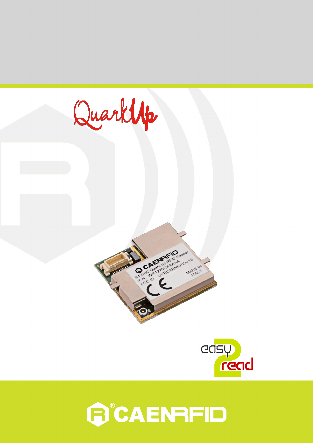
R1270
500mW UHF RFID Ultra Compact Module
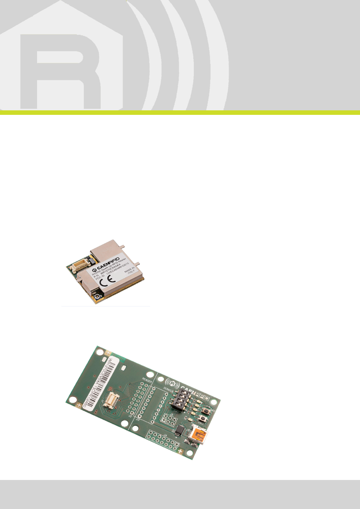
R1270CEVB
Quark Up Reader Evaluation Board

Scope of Manual
The goal of this manual is to provide the basic information to work with the Quark Up R1270 500mW UHF RFID Ultra
Compact Module.
Change Document Record
Date Revision Changes Pages
12 Oct 2016 01 First release -
18 May 2018 02
Modified REGULATORY COMPLIANCE chapter 29
Modified Technical Specifications Table 10
Added USB Communication Setup 27
Modified R1270 Quark up photo 1-6
4 June 2018 02.1
Added information for FCC Class II Permissive Change:
- Dual antenna configuration
- Addition of 7R1251IUNFAA to approved antenna list
18,29
Reference Document
[RD1] EPCglobal: EPC Radio-Frequency Identity Protocols Class-1 Generation-2 UHF RFID Protocol for
Communications at 860 MHz – 960 MHz, Version 2.0.1 (April, 2015).
CAEN RFID srl
Via Vetraia, 11 55049 Viareggio (LU) - ITALY
Tel. +39.0584.388.398 Fax +39.0584.388.959
info@caenrfid.com
www.caenrfid.com
© CAEN RFID srl – 2018
Disclaimer
No part of this manual may be reproduced in any form or by any means, electronic, mechanical, recording, or
otherwise, without the prior written permission of CAEN RFID.
The information contained herein has been carefully checked and is believed to be accurate; however, no responsibility
is assumed for inaccuracies. CAEN RFID reserves the right to modify its products specifications without giving any
notice; for up to date information please visit www.caenrfid.com.
Visit the Quark Up R1270 web page, you will find the latest revision
of data sheets, manuals, certifications, technical drawings, software and firmware.
All you need to start using your reader in a few clicks!

Federal Communications Commission (FCC) Notice (Preliminary)
This device was tested and found to comply with the limits set forth in Part 15 of the FCC Rules. Operation is subject to
the following conditions: (1) this device may not cause harmful interference, and (2) this device must accept any
interference received including interference that may cause undesired operation. These limits are designed to provide
reasonable protection against harmful interference when the equipment is operated in a commercial environment.
This device generates, uses, and can radiate radio frequency energy. If not installed and used in accordance with the
instruction manual, the product may cause harmful interference to radio communications. Operation of this product in
a residential area is likely to cause harmful interference, in which case, the user is required to correct the interference
at their own expense. The authority to operate this product is conditioned by the requirements that no modifications
be made to the equipment unless the changes or modifications are expressly approved by CAEN RFID.
Disposal of the product
Do not dispose the product in municipal or household waste. Please check your local regulations for
disposal/recycle of electronic products.

4
Index
Scope of Manual ...........................................................................................................................................................................2
Change Document Record ............................................................................................................................................................2
Reference Document ....................................................................................................................................................................2
Index 4
List of Figures ................................................................................................................................................................................. 4
List of Tables .................................................................................................................................................................................. 5
1
INTRODUCTION ................................................................................................................................................................... 6
Product Description ......................................................................................................................................................................6
Reader ..............................................................................................................................................................................6
Evaluation Board ..............................................................................................................................................................6
Accessories ...................................................................................................................................................................................7
R1270 Quark Up Reader Accessories ...............................................................................................................................7
R1270CEVB Quark Up Evaluation Board Accessories .......................................................................................................7
Development Kit ...........................................................................................................................................................................8
Ordering Options ..........................................................................................................................................................................8
Installation Notice ........................................................................................................................................................................9
2
QUARK UP R1270 .............................................................................................................................................................. 10
Technical Specifications Table ....................................................................................................................................................10
External Connections ..................................................................................................................................................................11
R1270 supply and I/O connector electrical characteristics ............................................................................................13
Power supply connection ...............................................................................................................................................14
General purpose I/O connections ..................................................................................................................................15
External reset .................................................................................................................................................................15
UART connection ...........................................................................................................................................................16
USB connection ..............................................................................................................................................................17
Dual multiplexed antenna configuration .......................................................................................................................18
Antenna port specifications ...........................................................................................................................................18
Reader – Tag Link Profiles ...........................................................................................................................................................19
Firmware Upgrade ......................................................................................................................................................................19
BSL operation .................................................................................................................................................................19
Firmware upgrade via R1270CEVB board ......................................................................................................................20
PCB Pad Layout ...........................................................................................................................................................................22
3
QUARK UP R1270CEVB ...................................................................................................................................................... 23
Technical Specifications Table ....................................................................................................................................................23
Connection diagram ...................................................................................................................................................................24
Installation Notice ......................................................................................................................................................................24
Technical drawings .....................................................................................................................................................................24
Electrical scheme ........................................................................................................................................................................25
External Connections ..................................................................................................................................................................26
USB Communication Setup .........................................................................................................................................................27
4
REGULATORY COMPLIANCE............................................................................................................................................... 29
FCC Compliance (Preliminary) ....................................................................................................................................................29
CE Compliance ............................................................................................................................................................................30
RoHS EU Directive .......................................................................................................................................................................30
Quark Up CE Declaration of Conformity .....................................................................................................................................31
Quark Up FCC Grant ...................................................................................................................................................................31
List of Figures
Fig. 1.1: Quark Up R1270 500mW UHF RFID Ultra Compact Module ......................................................................................................6
Fig. 1.2: Quark Up R1270CEVB - Quark-Up Reader Evaluation Board .....................................................................................................6
Fig. 1.3: R1270CEVB Accessories .............................................................................................................................................................7
Fig. 1.4: R1270CXDK: R1270 - Development kit with reader, adapter, antennas, cable and demo tags .................................................8
Fig. 1.5: Connection of the R1270CEVB to the Quark Up R1270 module ................................................................................................9
Fig. 2.1: Quark Up R1270 technical drawings ........................................................................................................................................11
Fig. 2.2: Quark Up R1270 power supply connection ..............................................................................................................................14
Fig. 2.3: Quark Up R1270 GPIO connection example.............................................................................................................................15
Fig. 2.4: Quark Up R1270 external reset ................................................................................................................................................15
Fig. 2.5: Quark Up R1270 RS232 connection .........................................................................................................................................16
Fig. 2.6: Quark Up R1270 USB connection .............................................................................................................................................17

5
Fig. 2.7: BSL sequence ...........................................................................................................................................................................19
Fig. 2.8: PCB pad layout .........................................................................................................................................................................22
Fig. 3.1: Quark Up R1270CEVB technical drawing .................................................................................................................................24
Fig. 3.2: Quark Up R1270CEVB electrical scheme ..................................................................................................................................25
Fig. 3.3: Quark Up R1270CEVB SMT pads ..............................................................................................................................................26
List of Tables
Tab. 2.1: Quark Up R1270 Technical Specifications ...............................................................................................................................10
Tab. 2.2: Quark Up R1270 connector pinout .........................................................................................................................................12
Tab. 2.3: Quark Up R1270 supply and I/O connector electrical characteristics .....................................................................................14
Tab. 2.4: RF port pinout .........................................................................................................................................................................18
Tab. 2.5: RF port electrical characteristics .............................................................................................................................................18
Tab. 2.6: Quark Up R1270 reader to tag link profiles ............................................................................................................................19
Tab. 3.1: R1270CEVB - Quark-Up Reader Evaluation Board ..................................................................................................................23
Tab. 3.2: Quark Up R1270CEVB GPIO connector pinout ........................................................................................................................26
Tab. 3.3: Quark Up R1270CEVB SMT pads signals .................................................................................................................................26
INTRODUCTION - Quark Up Technical Information Manual 6
1 INTRODUCTION
Product Description
Reader
The Quark-Up (Model R1270), OEM reader of the easy2read
©
Family, is an UHF multiregional ultra-compact reader for
low power, high performances UHF RFID applications.
With programmable output power in 18 steps from 10dBm to 27dBm, the reader can detect tags at more than 3 mt of
distance (depending on antenna and tag dimensions).
Due to its low power consumption, the module is specifically designed to be easily integrated in battery powered
devices.
The radio frequency core of the module permits to achieve fast reading and to be used in dense reader and dense tag
environments for top-class rated performances.
The compactness of the device and the board-to-board connector allow to embed the R1270 inside the new small form
factor industrial handhelds, smartphone accessories and other compact form factor devices.
The R1270 complies with and can operate in both European and US regulatory environments and due to its
multiregional capabilities, it's ideal for integration in devices requiring compliance to different geographical regions.
Fig. 1.1: Quark Up R1270 500mW UHF RFID Ultra Compact Module
Evaluation Board
The R1270CEVB evaluation board allows to manage the R1270 Quark Up reader directly via USB interface. This board
is particularly suited for Quark Up reader evaluation and SW development purposes.
Fig. 1.2: Quark Up R1270CEVB - Quark-Up Reader Evaluation Board
INTRODUCTION - Quark Up Technical Information Manual 7
Accessories
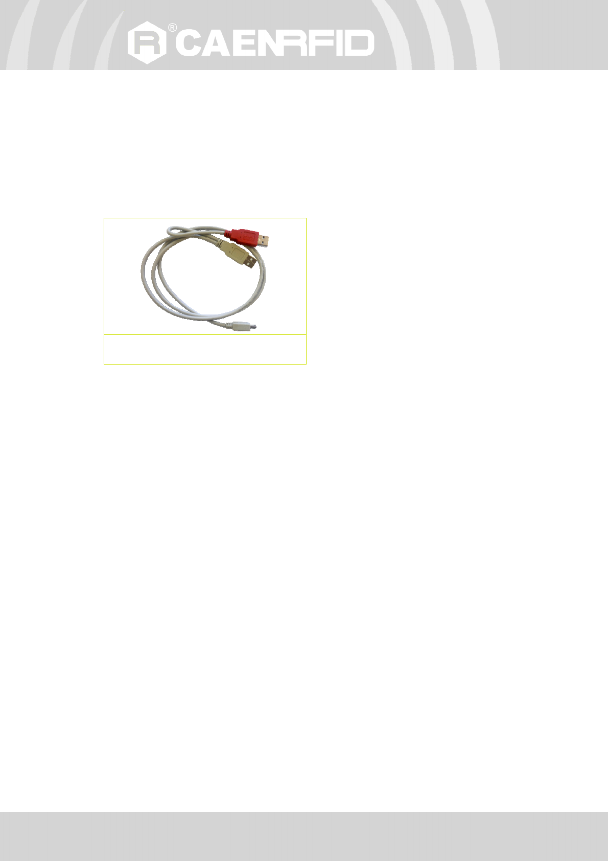
R1270 Quark Up Reader Accessories
None.
R1270CEVB Quark Up Evaluation Board Accessories
Check for the supplied accessories below:
No. 1 USB cable
Fig. 1.3: R1270CEVB Accessories
INTRODUCTION - Quark Up Technical Information Manual 8
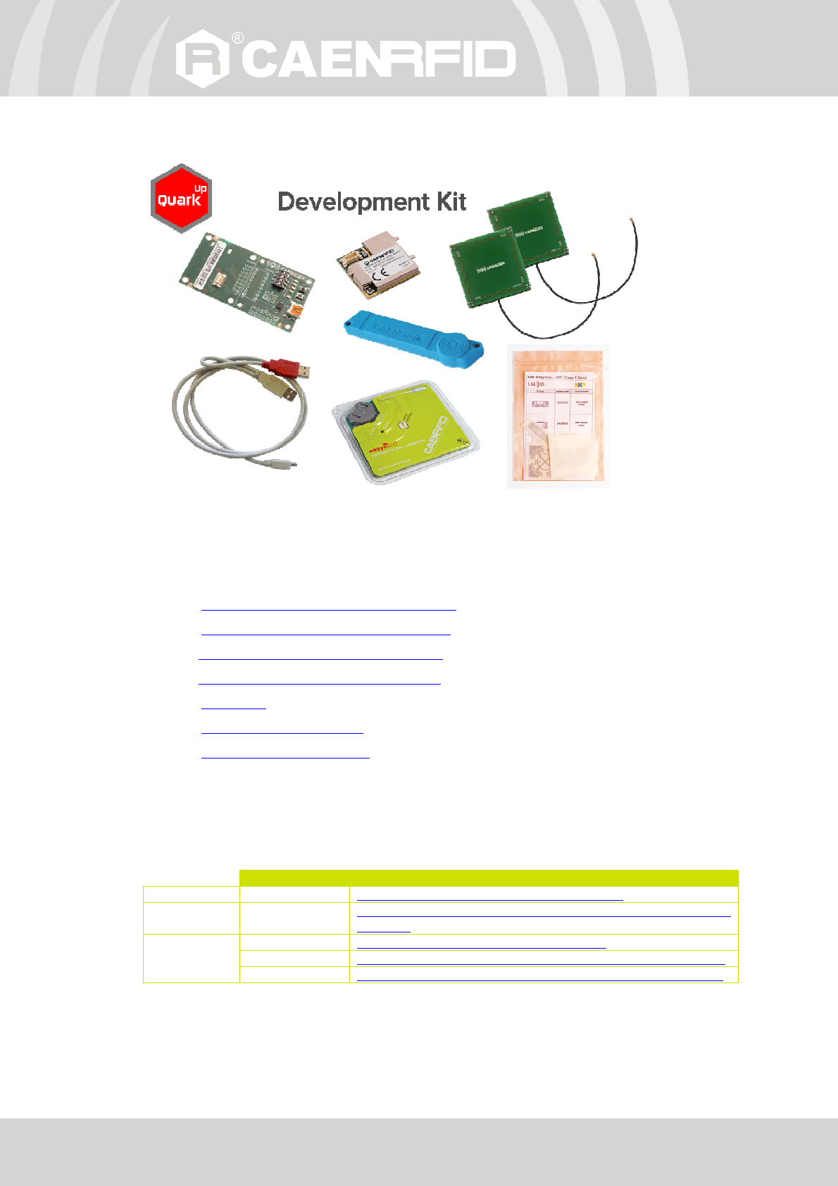
Development Kit
R1270CXDK – 500mW UHF RFID Ultra Compact Module Development Kit is available:
Fig. 1.4: R1270CXDK: R1270 - Development kit with reader, adapter, antennas, cable and demo tags
The R1270 Quark Up reader development kit is a complete RFID set up, for a quick implementation of RFID solutions. It
includes:
• n. 1 R1270 - 500mW UHF RFID Ultra Compact Module
• n. 1 R1270CEVB - Quark-Up Reader Evaluation Board
• n.1 Circular Polarized Quadrifilar Antenna U.FL ETSI
• n.1 Circular Polarized Quadrifilar Antenna U.FL FCC
• n. 1 Set of Labels
• n. 1 A927Z Temperature Logger Tag
• n. 1 RT0005 Temperature Logger Tag
• n. 1 USB cable
Ordering Options
Code Description
Reader WR1270CXAAAA R1270 - Ultra Compact Embedded UHF RFID Reader
Development
kit WR1270CXDKAA R1270 - Development kit with reader, adapter, antennas, cable and
demo tags
Accessories
WR1270CEVBXA R1270CEVB - Quark-Up Reader Evaluation Board
WANT020XAUFL ANT020/UFL - Quad - Circular polarized quadrifilar antenna (ETSI) - U.FL
WANT021XAUFL ANT021/UFL - Quad - Circular polarized quadrifilar antenna (FCC) - U.FL
INTRODUCTION - Quark Up Technical Information Manual 9
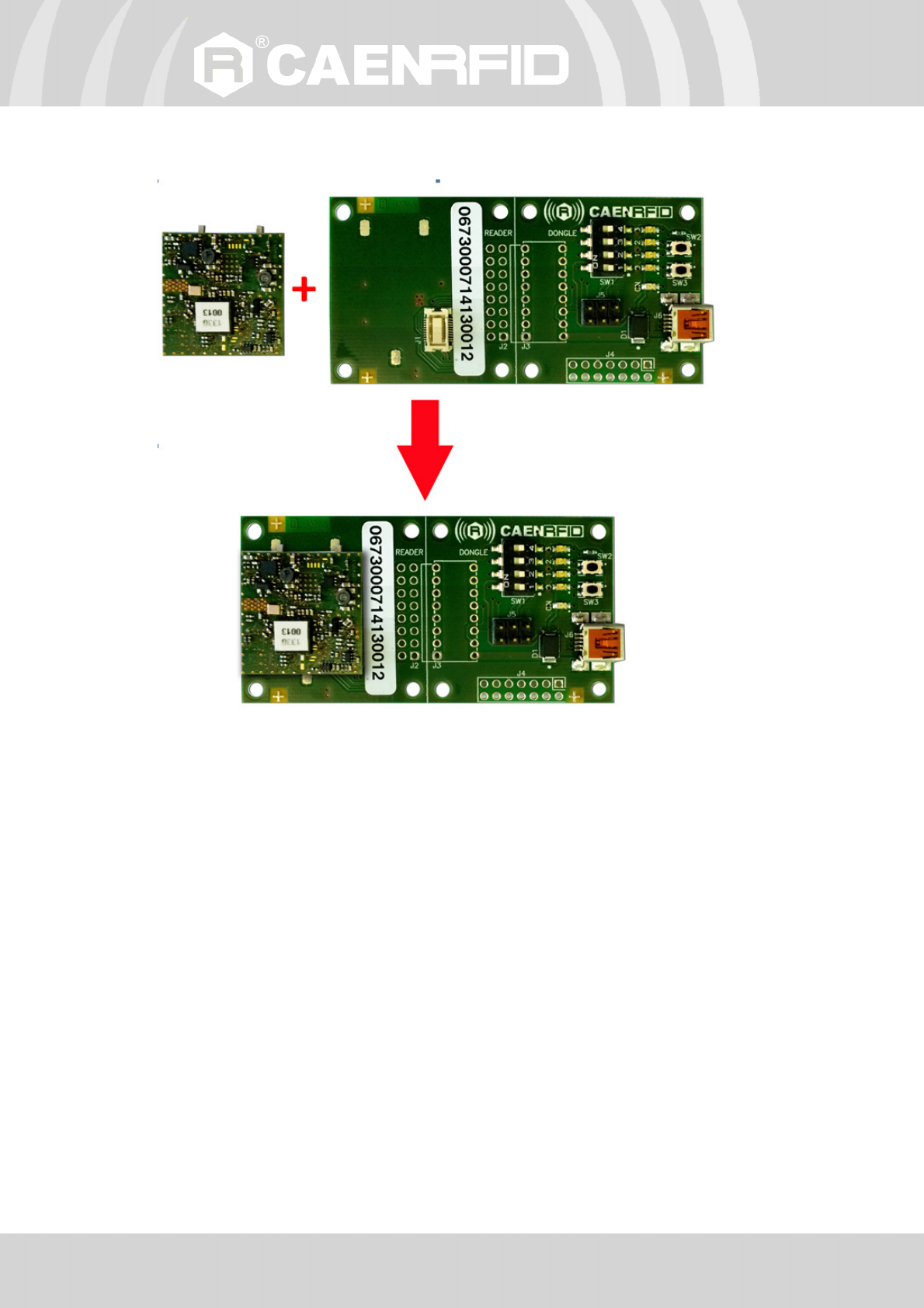
Installation Notice
The correct way to connect the Quark Up R1270 module to the evaluation board is shown in the following pictures:
Fig. 1.5: Connection of the R1270CEVB to the Quark Up R1270 module

QUARK UP R1270 - Quark Up Technical Information Manual 10
2 QUARK UP R1270
Technical Specifications Table
Frequency Band 865.600÷867.600 MHz (ETSI EN 302 208 v3.1.1)
902÷928 MHz (FCC part 15.247)
RF Power Programmable in 18 levels (1dB step) from 10dBm to 27dBm (from 10mW
to 500mW) conducted
Output Power Accuracy +/- 1dB
Antenna VSWR Requirement 2:1 or better for optimum performances
Antenna Connector Nr. 1 U.FL type
Frequency Tolerance ±10 ppm over the entire temperature range
Number of Channels 4 channels (compliant to ETSI EN 302 208 v3.1.1)
50 hopping channels (compliant to FCC part 15.247).
Standard Compliance EPC C1G2 [RD1]/ISO 18000-63
Digital I/O 4 I/O lines (3.3V level; Iout=3mA max)
Connectivity
USB interface:
One USB 2.0 Full Speed (12Mbit/s) device port
UART Serial Port:
Baudrate: up to 115200
Databits: 8
Stopbits: 1
Parity: none
Flow control: none
3.3 V I/O Voltage Level
DC Power 5.0 VDC+/-5%
Power Consumption
2.7W @ RF out = 27dBm
1.6W @ RF out = 23dBm
0.15W in idle mode
Operating Temperature -10 °C to +55 °C
Dimensions (W)25 x (L)25 x (H)6 mm
3
(1.0 x 1.0 x 0.2 inch
3
)
Weight 5 g
Tab. 2.1: Quark Up R1270 Technical Specifications
Warning: The RF settings must match the country/region of operating to comply with local laws and regulations.
It is not allowed the use in different countries/regions from the one in which the device has been sold.
Y
QUARK UP R1270 - Quark Up Technical Information Manual 11
External Connections
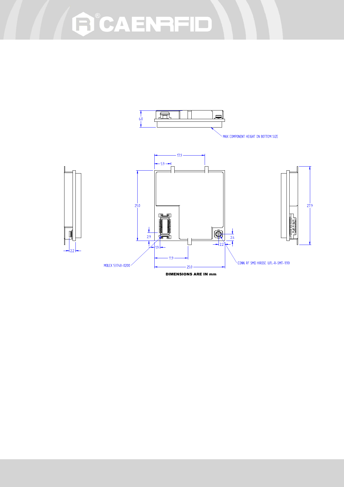
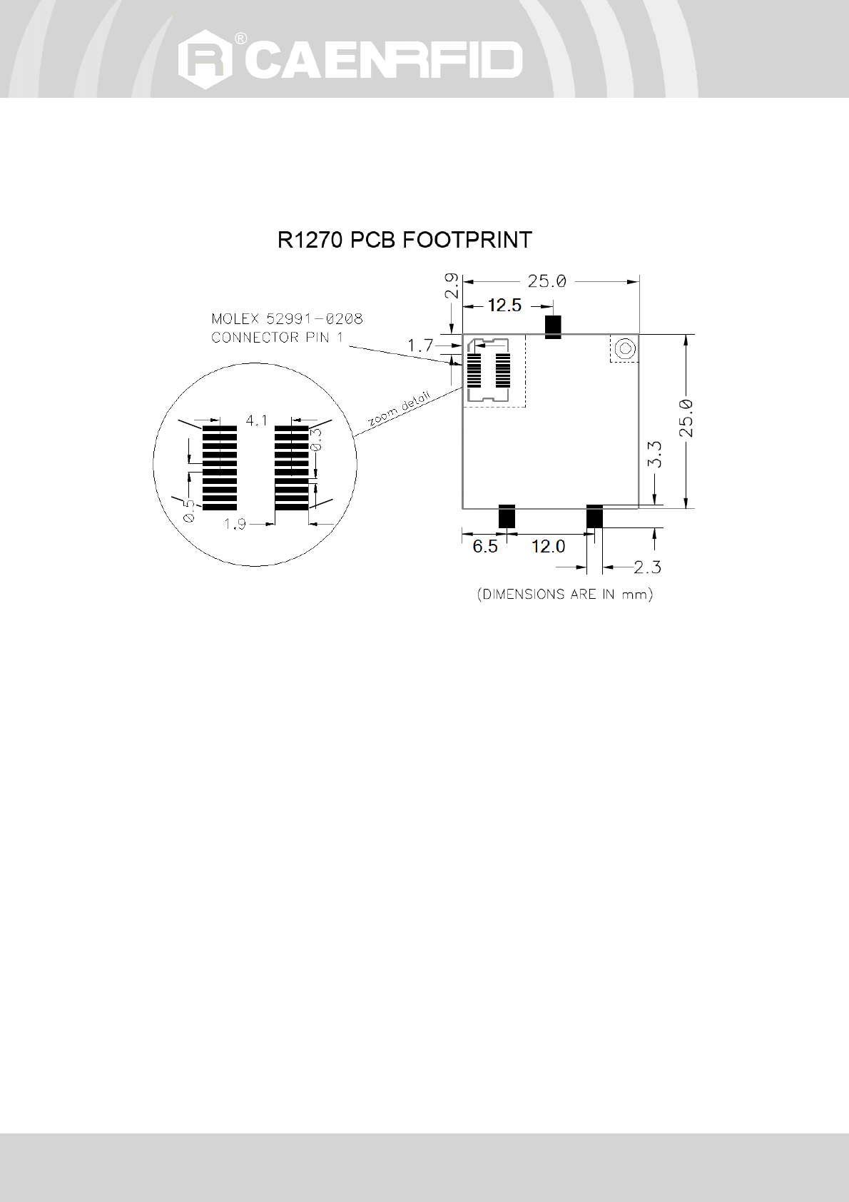
The location of the connectors is shown in Fig. 2.1. Their mechanical specifications are listed below:
Antenna Port: U.FL female (P.N. HIROSE: U.FL-R-SMT-1(10)).
Supply and I/O connector: Molex P.N. 53748-0208 (mates with Molex 52991-0208 to be used on the host board).
Fig. 2.1: Quark Up R1270 technical drawings
QUARK UP R1270 - Quark Up Technical Information Manual 12
Supply and I/O connector pinout is shown in the following table
1
:
Pin # Signal Description
1 GND Ground
2 TCK TCK JTAG signal (debug purpose only)
3 GND Ground
4 /RST Reset
5 TXD UART TX to host
6 TMS TMS JTAG signal (debug purpose only)
7 RXD UART RX from host
8 TDI TDI JTAG signal (debug purpose only)
9 5V_USB USB Vbus voltage
10 TDO TDO JTAG signal (debug purpose only)
11 BSL_SEL Bootloader interface selection
12 TST TST JTAG signal (debug purpose only)
13 D+ USB data +
14 GPIO0 General Purpose IO #0
15 D- USB data -
16 GPIO1 General Purpose IO #1
17 VIN Input supply voltage
18 GPIO2 General Purpose IO #2
19 VIN Input supply voltage
20 GPIO3 General Purpose IO #3
Tab. 2.2: Quark Up R1270 connector pinout
The GPIO0-GPIO3 pins are 4 general purpose bidirectional pins, their default direction at power up (or after a Reset) is
input.
The reader can be controlled via UART or USB interface. The selection of the interface is performed internally to the
module according to the following algorithm: if no interface has been previously selected and a high level signal is
detected on the RXD pin, the UART interface is selected and the USB interface is disabled; on the contrary if no
interface has been previously selected and RXD pin is at low level or left unconnected, the USB interface is selected and
the UART interface is disabled. Please note that in case you want to switch between the two interfaces you have to
reset the module.
For the USB interface a Virtual COM Port (VCP) is implemented.
To establish a link with the device using UART or VCP connection, you must configure your COM port as follows:
Baud rate: 115200
Parity: None
Data bits: 8
Stop bits: 1
Flow Control: none
JTAG pins, unless otherwise noted, are for internal debug purpose only and shall not be connected by the user.
/RST and BSL_SEL pins shall be properly driven to start the bootloader of R1270 embedded microcontroller in case the
user wants to upgrade the firmware image of the reader. In normal operation BSL_SEL shall be at low level or left
unconnected.
See § BLS operation page 19 for the description of the bootloader operation.
1
Debug purpose and unused pins should not be connected.
QUARK UP R1270 - Quark Up Technical Information Manual 13
R1270 supply and I/O connector electrical characteristics
2
Pin name Pin No. Parameter Min Type Max Unit
GND 1,3
TCK 2
VIL -0.3 0.75 V
VIH 1.5 3.6 V
Input current 10 μA
/RESET 4
VIL -0.3 0.6 V
VIH 1.65 3.6 V
Internal pull-up resistance 47 kΩ
Pulse width 10 μs
TXD 5
VOL 0 0.55 V
VOH 2.5 3.5 V
Output current 3.0 mA
TMS 6
VIL -0.3 0.75 V
VIH 1.5 3.6 V
Input current 10 μA
RXD 7
VIL -0.3 0.75 V
VIH 1.5 3.6 V
Input current 10 μA
TDI 8
VIL -0.3 0.75 V
VIH 1.5 3.6 V
Input current 10 μA
5V_USB 9 Input DC voltage 4.75 5.00 5.25 V
Input current 20 mA
TDO 10
VOL 0 0.55 V
VOH 2.5 3.5 V
Output current 3.0 μA
BSL_SEL 11
VIL -0.3 1.0 V
VIH 2.2 3.6 V
Internal pull-down resistance 10 kΩ
TST 12
VIL -0.3 0.75 V
VIH 1.5 3.6 V
Internal pull-down resistance 45 kΩ
D+,D- 13,15
VOL 0 0.3 V
VOH 2.8 3.6 V
Impedance 28 44 Ω
GPIO[0:3] 14, 16,
18, 20
VOL 0 0.55 V
VOH 2.5 3.5 V
Output current 3.0 mA
VIL -0.3 0.75 V
VIH 1.5 3.6 V
Input current 10 μA
2
Exceeding maximum values reported in the table may cause permanent damage to the model.
QUARK UP R1270 - Quark Up Technical Information Manual 14
Pin name Pin No. Parameter Min Type Max Unit
VIN
3
17,19
Input supply voltage 4.75 5.00 5.25 V
Supply current (idle) 30 mA
Supply current (RF ON @
23dBm)
0.32 A
Supply current (RF ON @
27dBm)
0.55 A
Tab. 2.3: Quark Up R1270 supply and I/O connector electrical characteristics
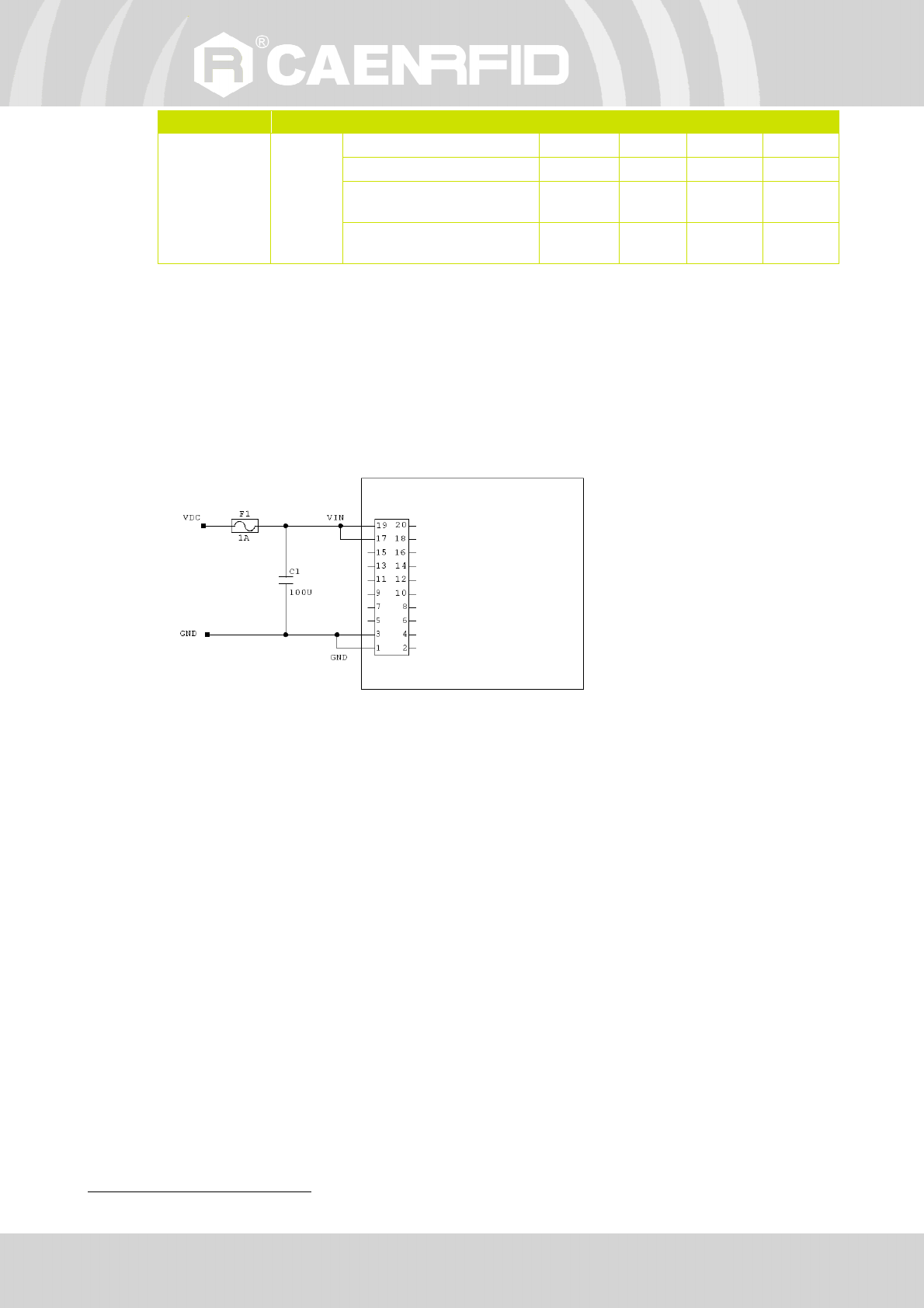
Power supply connection
In the following schematic suggested R1270 power supply connection is shown.
An external 100uF bypass capacitor between Vin and GND is recommended for proper operation.
The use of fuse F1 (or an equivalent solid state current limiter) is recommended since R1270 doesn't provide internal
current limitation protection.
Fig. 2.2: Quark Up R1270 power supply connection
3
External 100uF bypass capacitor between Vin and GND is recommended for proper operation.
Quark Up
Module
QUARK UP R1270 - Quark Up Technical Information Manual 15
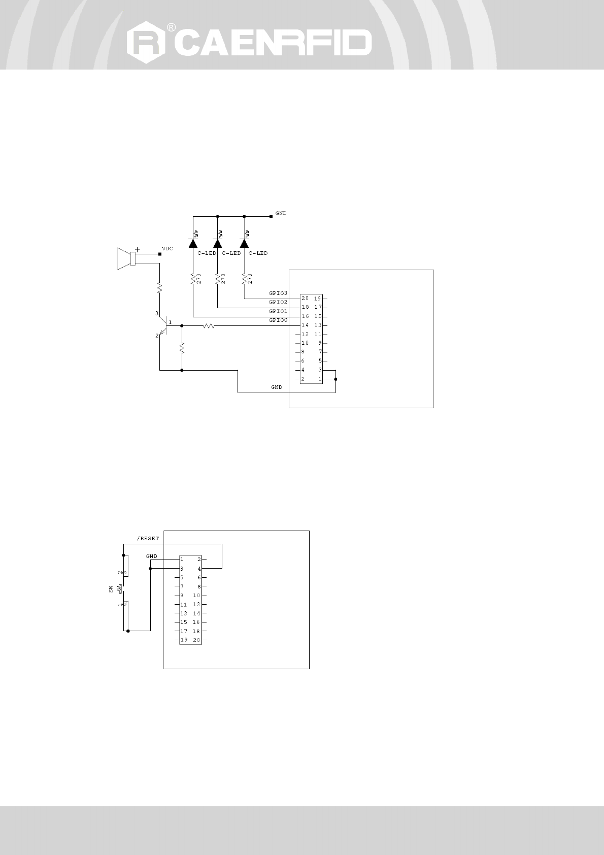
General purpose I/O connections
The GPIO0-GPIO3 pins are 4 general-purpose bidirectional pins. Their default direction after a power on reset or a
general reset is set to input.
GPIO, when configured as Outputs, can be used to drive indicators as LEDs or buzzers or to send trigger signal to others
equipments.
GPIO, when configured as Inputs, can accept control signals from other equipments or trigger signals from sensors (i.e.
photocells).
In the following schematic an example of application of GPIO is shown.
Fig. 2.3: Quark Up R1270 GPIO connection example
External reset
R1270 manual reset can be performed by forcing at low level /RESET pin for 10μs at least. /RESET pin is pulled-up by an
internal resistor.
Fig. 2.4: Quark Up R1270 external reset
Quark Up
Module
Quark Up
Module
QUARK UP R1270 - Quark Up Technical Information Manual 16
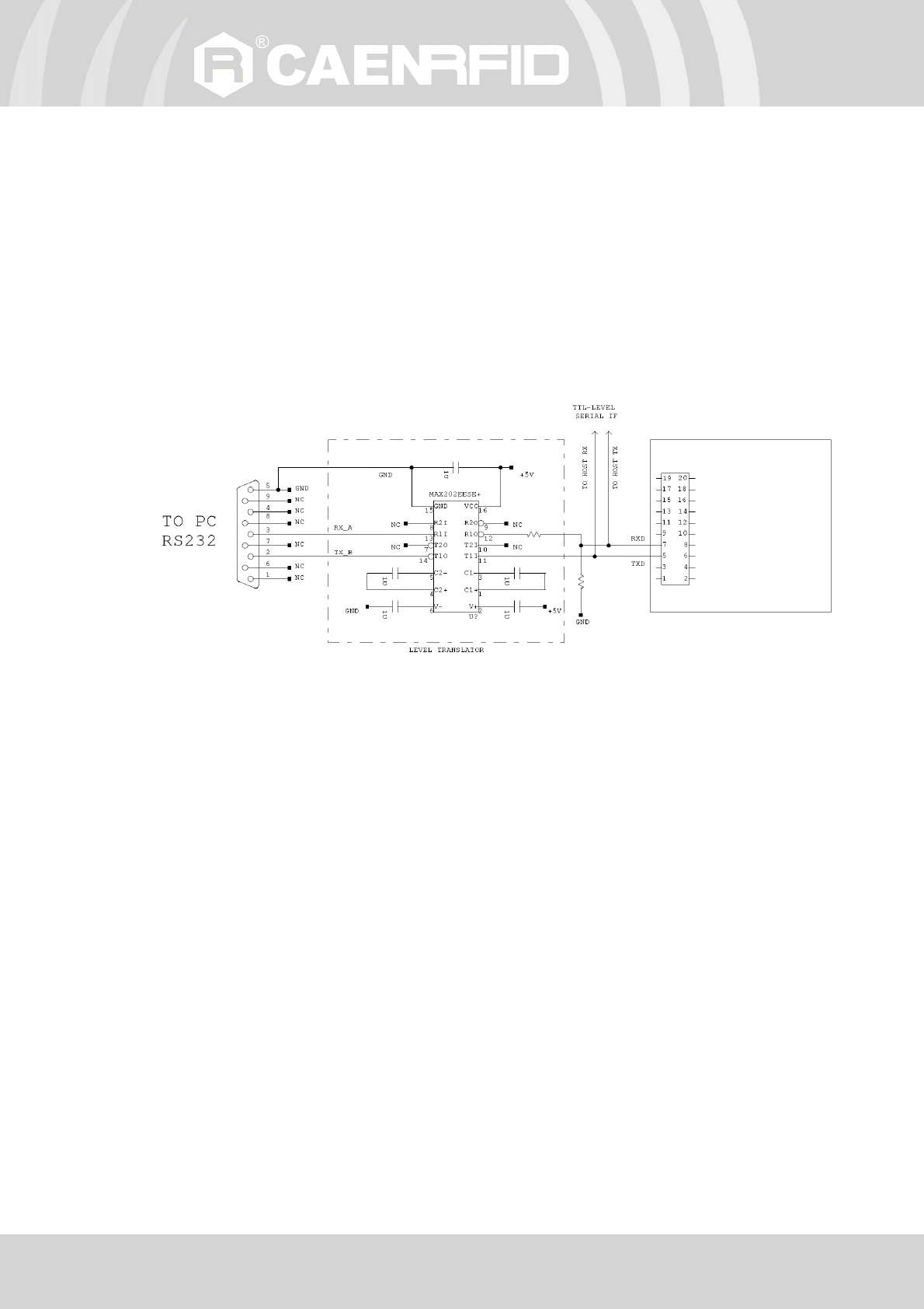
UART connection
The RXD/TXD pins are used to communicate with the R1270 board via UART port. Since Quark Up RX/TX are TTL level
signals, in order to connect it with a PC, a TTL/RS232 translator shall be used (please refer to the diagram below).
To establish a link with the device, the host COM port shall be configured as follows:
Baud rate: 115200
Parity: None
Data bits: 8
Stop bits: 1
Flow Control: none
Fig. 2.5: Quark Up R1270 RS232 connection
Quark Up
Module
QUARK UP R1270 - Quark Up Technical Information Manual 17
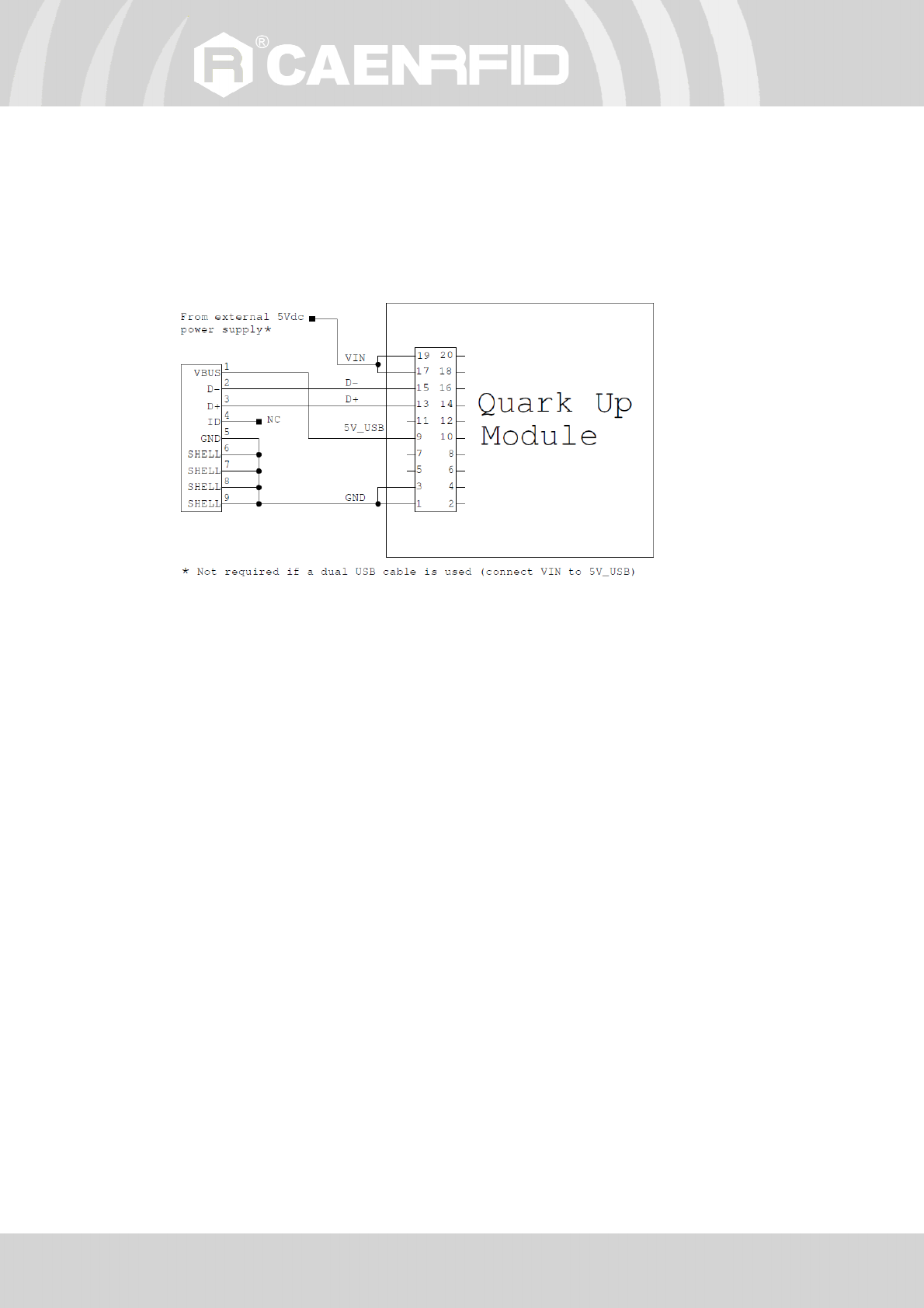
USB connection
In the following image the connection between R1270 module and USB interface is shown.
Since the maximum supply current for the reader exceeds the USB limitation (500mA), the supply voltage shall be
provided via an external power source or via a dual USB cable.
The 5V_USB signal at pin 9 of reader connector is not intended to supply the module but is used by the reader to
detect the presence of an USB host.
Fig. 2.6: Quark Up R1270 USB connection
A Virtual COM Port is implemented, in order to establish a link with the device, the host COM port shall be configured
as follows:
Baud rate: 115200
Parity: None
Data bits: 8
Stop bits: 1
Flow Control: none
The VID/PID combination that identifies the USB device is:
VID: 21E1
PID: 0080
QUARK UP R1270 - Quark Up Technical Information Manual 18
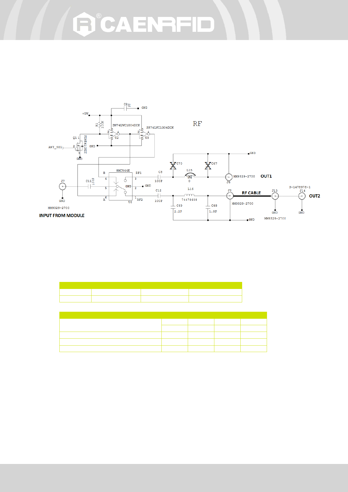
Dual multiplexed antenna configuration
The following application note is intended to provide the OEM manufacturer with the instructions in order to integrate
R1270C module in a dual multiplexed antenna scenario. Please note that only one antenna transmit at a time.
The circuit is based on Analog Device HMC544E RF switch and has an insertion loss of 0.25dB (typical). GPIO0 signal is
used to select the active switch port.
Fig. 7: Dual multiplexed antenna application note
Antenna port specifications
In the following table the pinout of R1270 antenna is shown.
Pin # Function Direction Description
INNER RF OUT OUT RF output
OUTER GND - Ground
Tab. 2.4: RF port pinout
Parameter Min Typ. Max Unit
RF output power 10 500 mW
10 27 dBm
Output power vs. power setting accuracy ± 1 dB
RF port impedance 50 Ω
Recommended antenna VSWR 2:1 -
Tab. 2.5: RF port electrical characteristics
QUARK UP R1270 - Quark Up Technical Information Manual 19
Reader – Tag Link Profiles
Quark Up reader supports different modulation and return link profiles according to EPC Class1 Gen2 protocol.
In the following table are reported all profiles that have been tested for the compliance with ETSI and FCC regulations.
Link profile # Regulation Modulation Return Link
0 ETSI - FCC PR–ASK; f=40kHz FM0; f = 40kHz
1 ETSI - FCC PR–ASK; f=40kHz Miller (M=4); f = 256kHz
4
2 ETSI - FCC PR–ASK; f=40kHz Miller (M=4); f = 320kHz
Tab. 2.6: Quark Up R1270 reader to tag link profiles
Firmware Upgrade
Quark Up reader firmware upgrade is based on Boot Start Loader (BSL) of the embedded microcontroller inside the
module.
An upgrade software has been developed to be used with Quark Up evaluation board (mod. R1270CEVB).
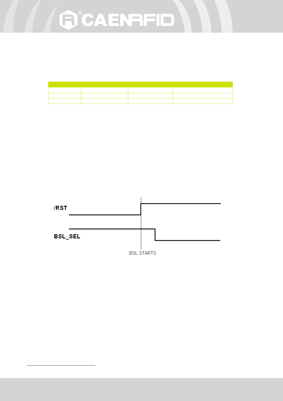
BSL operation
In order to start the BSL of Quark Up internal microcontroller /RST and BSL_SEL signal shall be driven as in the picture
below:
Fig. 2.8: BSL sequence
The BSL program execution starts if after a reset (or at power up) the BSL_SEL pin is at high level for at least 100ms.
The selected interface for upgrade operation is the USB and the protocol applied is defined as:
• HID protocol with one input endpoint and one output endpoint. Each endpoint has a length of 64 bytes.
• VID: 0x2047
• PID: 0x0200
4
Default value.
QUARK UP R1270 - Quark Up Technical Information Manual 20
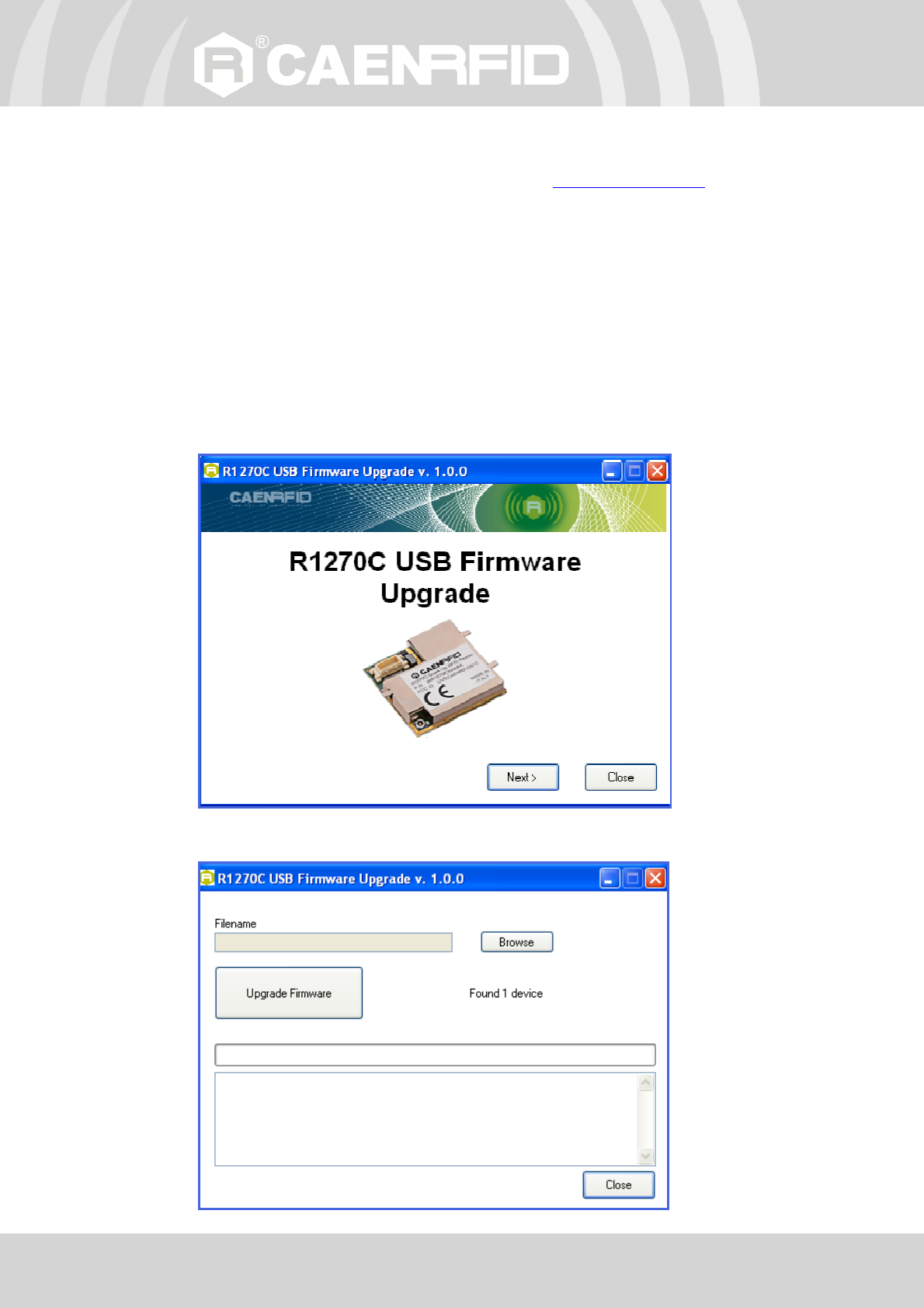
Firmware upgrade via R1270CEVB board
Quark Up firmware upgrade can be managed via USB by using the evaluation board (mod.R1270CEVB) and the SW
upgrade program. The Quark Up Upgrade Tool is available for free at Quark Up R1270 web page of the CAEN RFID Web
Site, Download section.
In order to upgrade the firmware follow the steps described below:
1. Connect to the USB port the evaluation board with the Quark Up reader installed.
2. Press the reset switch on the evaluation board (SW3).
3. With SW3 pressed, press the BSL_SEL switch on the evaluation board (SW2).
4. Release SW3.
5. Release SW2 within 1s respect to SW3.
6. Open the FW upgrade program.
7. Click on Next button.
8. In the window you will see the message “Found 1 device” (if the message is “No device connected” repeat the
points 2,3, 4 and 5).
QUARK UP R1270 - Quark Up Technical Information Manual 21
9. Select the FW image file by clicking on “Browse” button.
10. Click on “Upgrade Firmware” button and wait for the upgrade to be completed.
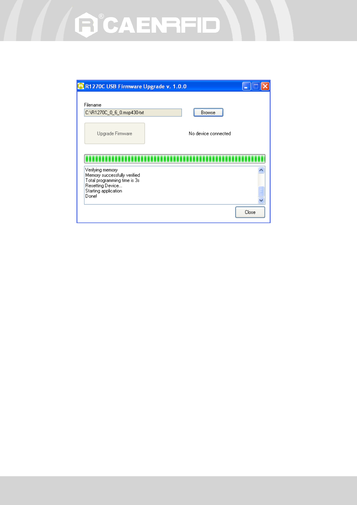
11. At the end of procedure, if the upgrade has been successfully performed, you will see the messages reported in
the image below and the module is ready for normal operation.
QUARK UP R1270 - Quark Up Technical Information Manual 22
PCB Pad Layout
In the picture below the recommended PCB pad layout to be implemented on the user host board is shown. The 3
square pads shall be used to solder R1270 shield and shall be connected to ground. In addition it is shown the position
and the layout required for Molex 52991-0208 connector, which mates with R1270 supply and I/O connector, and
which shall be soldered on the host board.
Fig. 2.9: PCB pad layout
1
19
2
20

QUARK UP R1270CEVB - Quark Up Technical Information Manual 23
3 QUARK UP R1270CEVB
Technical Specifications Table
Switch
SW1= GPIO
SW2= BSL_SEL
SW3= RESET
USB Port
Mini USB Type A plug connector
Bus powered USB 2.0 device
Must be connected to two High-power Port (500 mA @ VBUS) with a dual
USB cable.
It appears as USB serial port
Virtual Com Port (VCP)
5
drivers for Windows XP/Vista/Seven (7)
Baudrate: 115200
Databits: 8
Stopbits: 1
Parity: none
Flow control: none
User Interface Red LED: Power
Green LED: GPIO[0..3].
Dimensions (W)38.0 x (L)76.0 x (H)12.0 mm
3
(1.5 x 3.0 x 0.5 inch
3
)
Electrical Power DC Voltage 5V +/-5%
Max 800 mA
6
Operating Temperature -10 °C to +55 °C
Tab. 3.1: R1270CEVB - Quark-Up Reader Evaluation Board
Warning: The RF settings must match the country/region of operating to comply with local laws and regulations.
The usage of the reader in different countries/regions from the one in which the device has been sold is not allowed.
5
You can download VCP drivers for Windows based systems from the CAEN RFID Web Site at Quark Up R1270 page.
6
With Quark Up reader operating.
Y
QUARK UP R1270CEVB - Quark Up Technical Information Manual 24
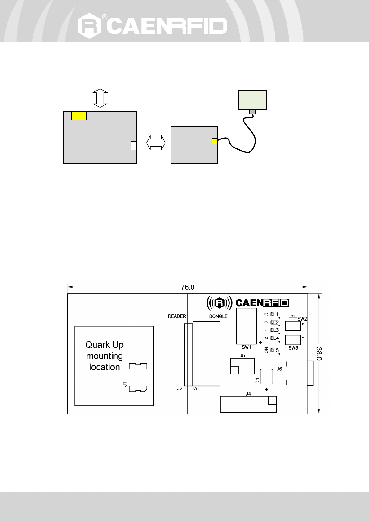
Connection diagram
The following block diagram shows how to connect the Mod. R1270 with the PC host via the Mod.
R1270CEVB
evaluation board.
Installation Notice
Refer to § Installation Notice page 9 for the correct way to connect the Quark Up R1270 module to the evaluation
board.
Technical drawings
The location of the connectors is shown in Fig. 3.1. Their mechanical specifications are listed below.
All dimensions are in millimeters.
Fig. 3.1: Quark Up R1270CEVB technical drawing
Antenna
USB
R1270CEVB
Molex Connector
R1270
Ultra Compact
Embedded UHF
RFID Reader
to host
QUARK UP R1270CEVB - Quark Up Technical Information Manual 25
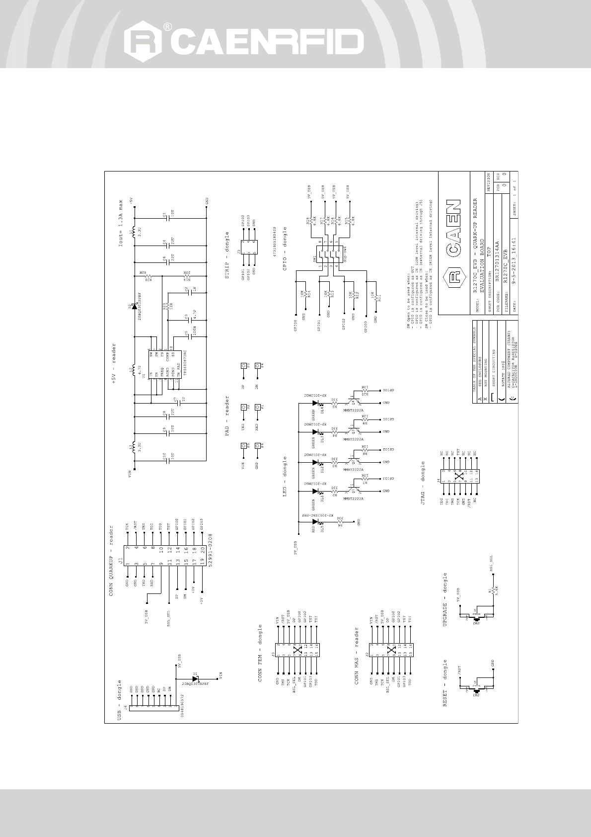
Electrical scheme
The electrical scheme of the Quark Up R1270CEVB is shown in Fig. 3.2: Quark Up R1270CEVB electrical scheme.
The board hosts an embedded DC/DC boost converter that is used to compensate voltage drop across USB cable.
This circuit can be used as a reference design for standard 3.7V battery applications.
Fig. 3.2: Quark Up R1270CEVB electrical scheme
QUARK UP R1270CEVB - Quark Up Technical Information Manual 26
External Connections
GPIO connector pinout (J5) is shown in the following table:
Pin # Signal
1 GPIO 1
2 GPIO 0
3 GPIO 2
4 GPIO 3
5 GND
6 GND
Tab. 3.2: Quark Up R1270CEVB GPIO connector pinout
J4 (not populated) is the JTAG connector for internal debug purposes and shall not be used.
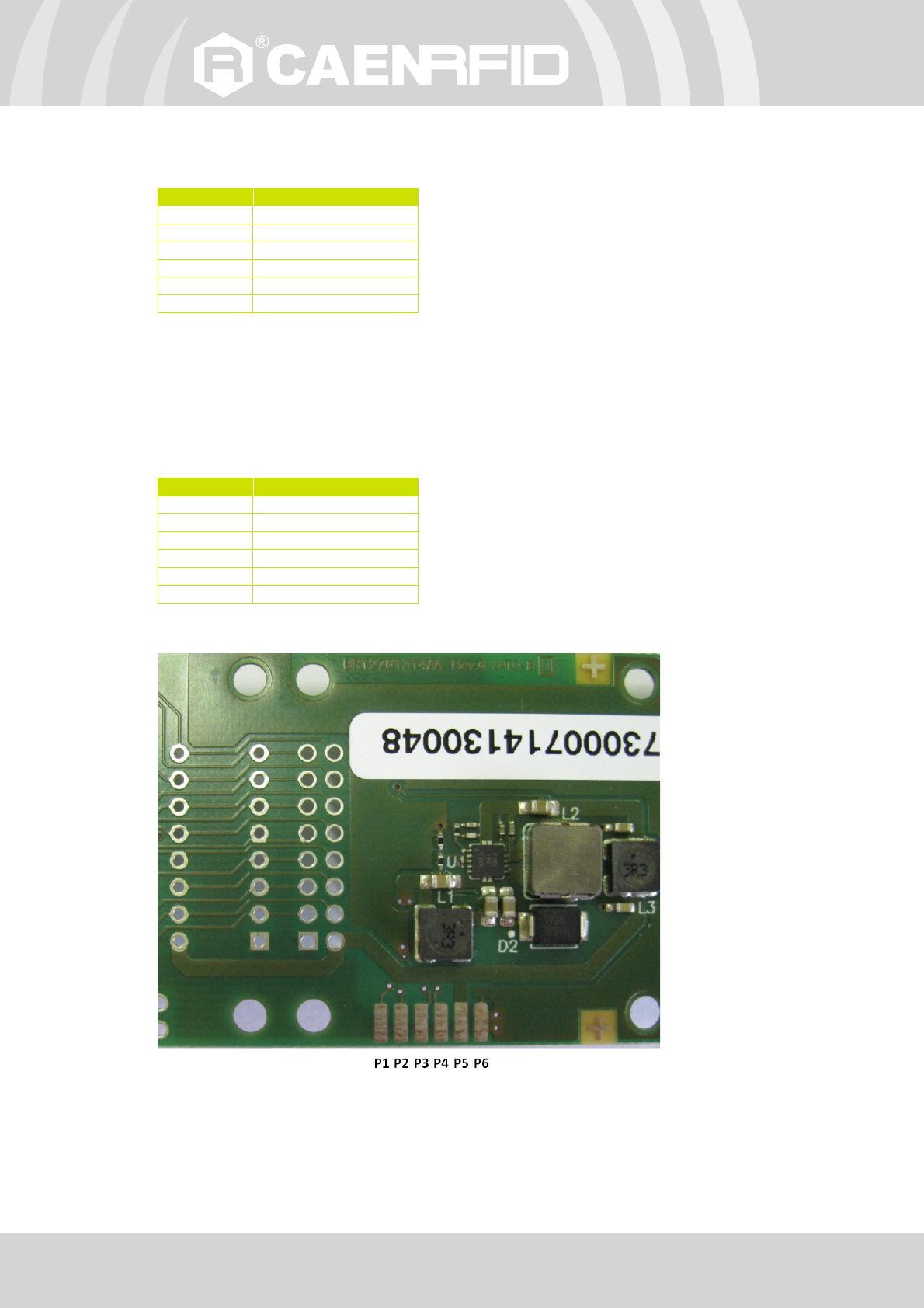
In case an OEM manufacturer wants to connect the module to its own device for testing purposes, SMT pads are
present on the bottom side of the board for power supply, UART and USB signals.
Pad # Signal
P1 RXD
P2 TXD
P3 D+
P4 D-
P5 Vin (2.5Vdc ÷ 4.5Vdc)
P6 GND
Tab. 3.3: Quark Up R1270CEVB SMT pads signals
Fig. 3.3: Quark Up R1270CEVB SMT pads
QUARK UP R1270CEVB - Quark Up Technical Information Manual 27
USB Communication Setup
The Quark reader can be connected to a PC using the evaluation board and it is detected by the PC as an emulated
serial port. In order to correctly operate with the reader you need to install a driver:
1. Connect the Quark Up R1270 module to the evaluation board as shown in the § Installation Notice page 9 and
then to a PC using the provided USB cable.
2. A dialog window appears informing you that the device is not recognized. In order to correctly operate with the
reader you need to install the VCP (Virtual Com Port) drivers for your operating system. You can download VCP
drivers for Windows based systems from the CAEN RFID Web Site from the Quark Up R1270 web page, Downloads
section or from the Software and Firmware download area.
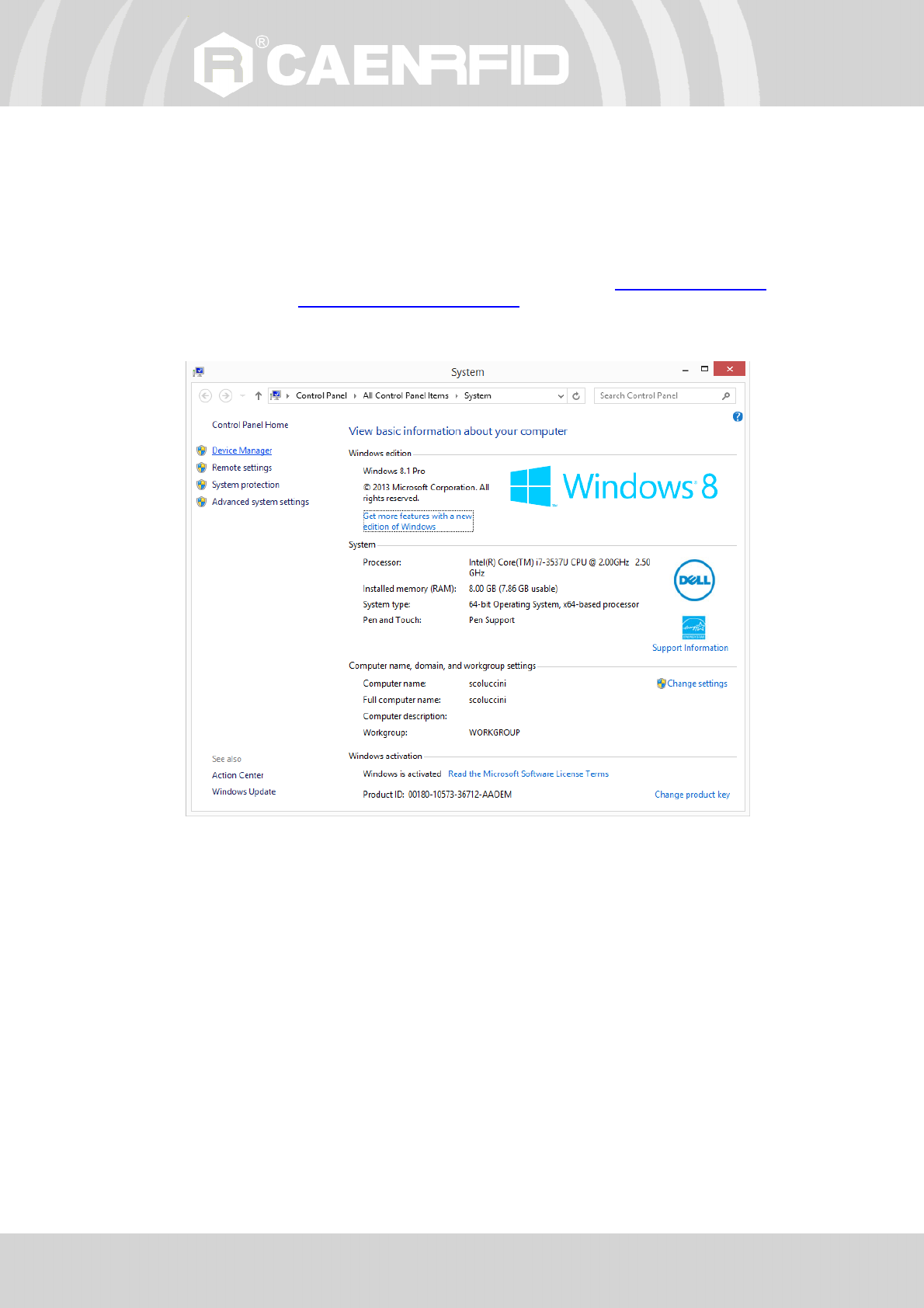
3. Open the System properties: go to Control Panel → All Control Panel Items → System and click on Device
Manager.
QUARK UP R1270CEVB - Quark Up Technical Information Manual 28
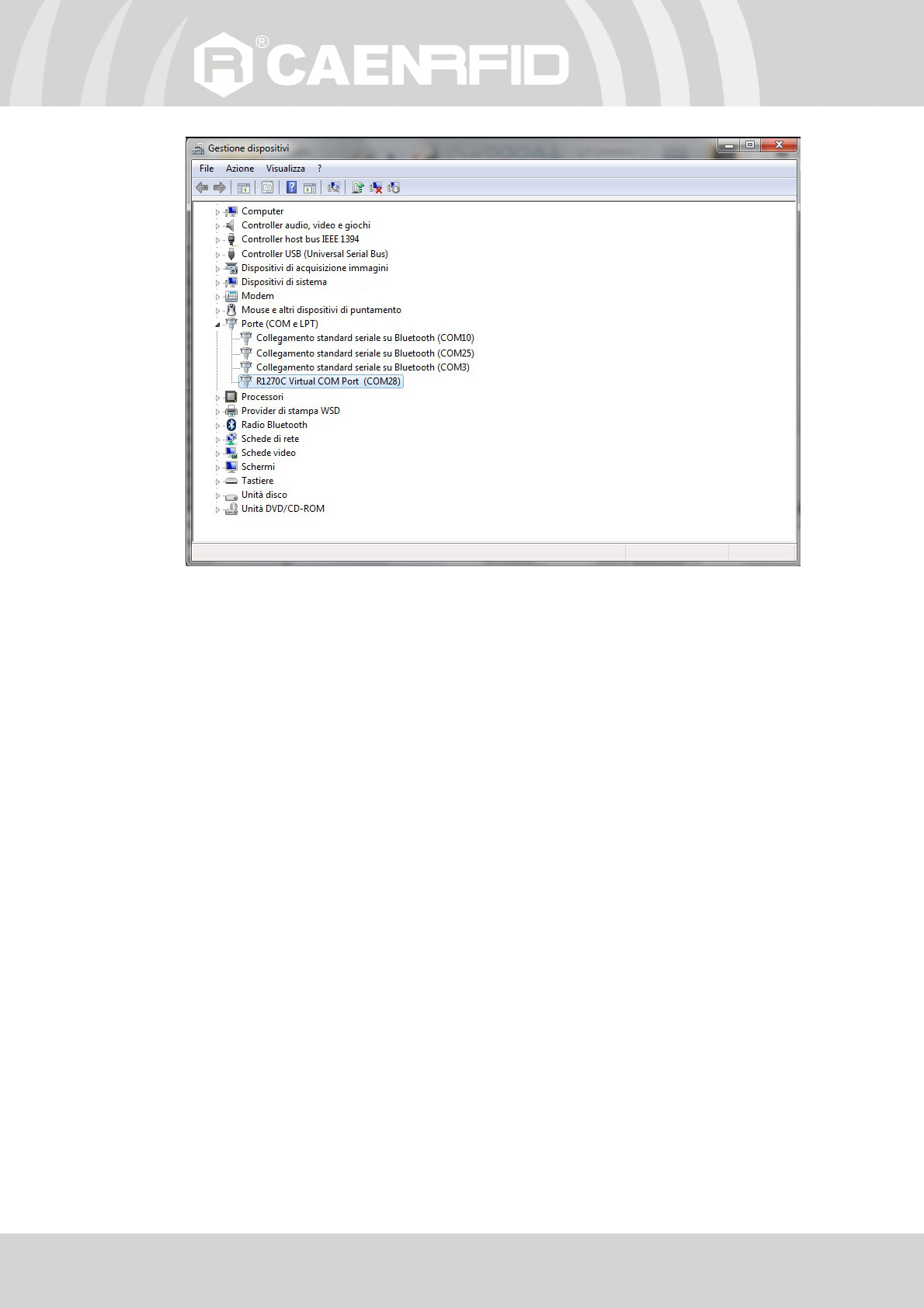
4. After having installed the driver, the reader is detected by the PC as an emulated serial port (VCP):

REGULATORY COMPLIANCE - Quark Up Technical Information Manual 29
4 REGULATORY COMPLIANCE
FCC Compliance (Preliminary)
This equipment has been tested and found to comply with Part 15 of the FCC Rules.
NOTE:
a. Any changes or modification not approved by CAEN RFID could void the user’s authority to operate the
equipment.
b. The Quark Up R1270 Module, which is rated at 500 mW output, is approved for operation with the following
antennas:
- QUAD - Circular Polarized Quadrifilar Antenna (CAEN RFID mod. WANTENNAX010) with 0.7dBi gain.
- UHF Near Field Antenna (CAEN RFID mod. 7R1251IUNFAA) with -8dBi gain.
Use of other than the approved antennas with this unit may result in harmful interference with other users, and
cause the unit to fail to meet regulatory requirements.
c. This transmitter module is authorized to be used in other devices only by OEM integrators under the following
conditions:
1. The RFID Module antenna shall have a separation distance of at least 20 cm from all persons
2. The transmitter module must not be co-located with any other antenna or transmitter
d. In case that the two conditions above are met, further transmitter testing will not be necessary. However, the
OEM integrator is still responsible for testing the end-product for any additional compliance requirements
required with this module installed (for example, digital device emissions, PC peripheral requirements, etc.). In the
event that these conditions cannot be met (for certain configurations or co-location with another transmitter),
then the FCC authorization is no longer considered valid and the FCC ID cannot be used on the final product. In
such case the OEM integrator will be responsible for re-evaluating the end product (including the transmitter) and
obtaining a separate FCC authorization.
e. If the FCC ID is not visible when the module is installed inside another device, the OEM integrator shall apply a
label in a visible area on his product with the following statement:
Contains Transmitter Module FCC ID: UVECAENRFID015
or
Contains FCC ID: UVECAENRFID015
f. The OEM integrator has to be aware not to provide information to the end user regarding how to install or
remove this RF module or change RF related parameters in the user manual of the end product.

REGULATORY COMPLIANCE - Quark Up Technical Information Manual 30
CE Compliance
Reference standard:
ETSI EN 301 489-1 V. 1.9.2:2011
EN 55032:2012
CEI EN 55024:2013
ETSI EN 302 208 V3.1.1:2017
CEI EN 60950-1:2007 +/A11:2010 +/A1:2012 +/A12:2012
CEI EN 50364:2011
EN 50581:2012
See § Quark Up CE Declaration of Conformity page 31 for the Quark Up R1270 CE Compliance Certificate.
RoHS EU Directive
The Quark Up R1270 UHF RFID Ultra Compact Module is compliant with the EU Directive 2011/65/EU on the
Restriction of the Use of certain Hazardous Substances in Electrical and Electronic Equipment (RoHS2).

R1270
CE DECLARATION OF CONFORMITY
Quark Up CE Declaration of Conformity
We
CAEN RFID Srl
Via Vetraia, 11
55049 Viareggio (LU)
Italy
Tel.: +39.0584.388.398 Fax: +39.0584.388.959
Mail: info@caenrfid.com
Web site: www.caenrfid.com
herewith declare under our own responsibility that the product:
Code: WR1270CXAAAA
Description: R1270 - Ultra Compact Embedded UHF RFID Reader
corresponds in the submitted version to the following standards:
ETSI EN 301 489-1 V. 1.9.2:2011
EN 55032:2012
CEI EN 55024:2013
ETSI EN 302 208 V3.1.1:2017
CEI EN 60950-1:2007 +/A11:2010 +/A1:2012 +/A12:2012
CEI EN 50364:2011
EN 50581:2012
and declare under our sole responsibility that the specified product meets the principle requirements and other applicable
regulations of directives 2014/53/EU (RED) and 2011/65/EU (RoHS2)
Date: 08/01/2018
Adriano Bigongiari (Chief Executive Officer)
On the basis of this declaration, these products will bear the following mark:
Quark Up FCC Grant