CIMCON Lighting CIM35X1 CIMX1PRO RF MODULE User Manual
CIMCON Lighting, Inc. CIMX1PRO RF MODULE
User Manual

RF Module
Model: CIMX1PRO
Product Manual
CIMCON Lighting, Inc.
234 Littleton Road
Westford, MA 01886.
www.cimconlighting.com
Document No. RFM-PM-100-010-A
Confidential

Product Manual
RF Module
This information is confidential and proprietary to CSI and is to be used only for the purpose for which it is provided. Reproduction by any means,
electronic or mechanical, and distribution to third parties without express written permission from CSI is not permitted.
No part of this document may be reproduced or transmitted in any form or by any means, electronic
or mechanical, for any purpose, without the express written permission of CIMCON Lighting, Inc.
Information in this document is subject to change without notice. CIMCON Lighting, Inc. may have
patents or pending patent applications, trademarks, copyrights, or other intellectual property rights
covering subject matter in this document. The furnishing of this document does not give you license
to these patents, trademarks, copyrights, or other intellectual property except as expressly provided in
any written license agreement from CIMCON Lighting, Inc.
© 2013 CIMCON Lighting, Inc.
All rights reserved.

Product Manual
RF Module
i
This information is confidential and proprietary to CSI and is to be used only for the purpose for which it is provided. Reproduction by any
means, electronic or mechanical, and distribution to third parties without express written permission from CSI is not permitted.
T
Ta
ab
bl
le
e
o
of
f
C
Co
on
nt
te
en
nt
ts
s
1 GETTING STARTED ......................................................................................... 1-1
1.1. OVERVIEW ................................................................................................................................... 1-1
1.2. KEY FEATURES ............................................................................................................................. 1-1
1.3. FCC APPROVALS ......................................................................................................................... 1-2
1.4. FCC LABELING REQUIREMENTS .................................................................................................. 1-2
2 SMT MODULE PIN-OUT.................................................................................. 2-1
3 THROUGH HOLE MODULE PIN-OUT ............................................................. 3-4
4 CONFIGURATION INFORMATION ................................................................. 4-1
4.1. ABSOLUTE MAXIMUM RATINGS OF RF MODULE........................................................................... 4-1
4.2. RECOMMENDED OPERATING CONDITIONS ................................................................................... 4-1
4.3. DC ELECTRICAL CHARACTERISTICS.............................................................................................. 4-1
4.4. POWER SETTINGS FOR REGULATORY COMPLIANCE ....................................................................... 4-2
5 BOARD LAYOUT .............................................................................................. 5-1
6 SOLDERING TEMPERATURE PROFILE .......................................................... 6-1
6.1. LEADED PROCESS ........................................................................................................................ 6-1
6.2. LEAD FREE PROCESS ................................................................................................................... 6-1
7 MECHANICAL DIMENSIONS OF THE SMT MODULES .................................... 7-1
8 MECHANICAL DIMENSIONS FOR THROUGH HOLE MODULE ...................... 8-1

Product Manual
RF Module
1-1
This information is confidential and proprietary to CSI and is to be used only for the purpose for which it is provided. Reproduction by any means,
electronic or mechanical, and distribution to third parties without express written permission from CSI is not permitted.
1
1
G
GE
ET
TT
TI
IN
NG
G
S
ST
TA
AR
RT
TE
ED
D
1.1. Overview
This manual describes the key features, pin out, recommended operating conditions, working of
RF module and operating instructions to test the module for FCC.
CIMCON RF modules are designed to operate within the ZigBee protocol and support the unique
needs of low-cost, low-power wireless sensor networks. The modules require minimal power and
provide reliable delivery of data between remote devices. The modules operate within the ISM 2.4
GHz frequency band work on ZigBee protocol.
1.2. Key Features
The key features of RF modules are as follows:
• Operates from wide 2.1VDC to 3.6VDC
• Maximum transmit current is 150mA (Typical at 3.0V)
• Maximum Receive current is 38mA
• Maximum transmit power is +22dBm
• Receiver Sensitivity of -104dBm
• Various serial interfaces like UART, SPI (master/ slave), and TWI
• Six external ADC sources with 14-bit resolution
• Urban range of ~85m
• Line of sight range of ~1750m

Product Manual
RF Module
1-2
This information is confidential and proprietary to CSI and is to be used only for the purpose for which it is provided. Reproduction by any means,
electronic or mechanical, and distribution to third parties without express written permission from CSI is not permitted.
1.3. FCC Approvals
The CIMCON SMT module and through hole module with the integrated wire whip Antenna
as well as the SMT module and through hole including the 2.1dBi external antenna complies
with FCC CFR Part 15 (USA). The devices meet the requirements for modular transmitter
approval.
External Antennas:
Dipole Antenna (P/N: A24-HASM-525; Maximum Antenna Gain: 2.1dBi)
Dipole Antenna (P/N: A24-HASM-450; Maximum Antenna Gain: 2.1dBi)
This device complies with Part 15 of the FCC rules. Operation is subject to the following two
conditions:
1) This device may not cause harmful interference.
2) This device must accept any interference received, including interference that may cause
undesired operation.
Changes and Modifications not expressly approved by CIMCON can void your
authority to operate this equipment under Federal Communications Commission’s
rules.
The following statement must be included as a CAUTION statement in manuals for OEM
products to alert users on FCC RF exposure compliance:
“WARNING: To satisfy FCC RF exposure requirements for mobile transmitting devices, a
separation distance of 20 CM or more should be maintained between the antenna of this device
and persons during operation. To ensure compliance, operations at closer
distances than this are not recommended.”
1.4. FCC Labeling Requirements
When integrating the CIMCON’s SMT module or TH module into a product it must be ensured
that the FCC labeling requirements are met. This includes a clearly visible label on the outside of
the finished product specifying the CIMCON’s FCC identifier (FCC ID: S3Z-CIM35X1) as well as
the notice above. This exterior label can use wording such as “Contains Transmitter Module FCC
ID: S3Z-CIM35X1” or “Contains FCC ID: S3Z-CIM35X1” although any similar wording that
expresses the same meaning may be used.
Product Manual
RF Module
2-1
This information is confidential and proprietary to CSI and is to be used only for the purpose for which it is provided. Reproduction by any means,
electronic or mechanical, and distribution to third parties without express written permission from CSI is not permitted.
2
2
S
SM
MT
T
M
MO
OD
DU
UL
LE
E
P
PI
IN
N-
-O
OU
UT
T
Following is the pin out of CIMCON RF module with description of each pin:
1
2
3
4
5
6
7
8
9
10
11
12
13
14
15
16
17
18
28
27
26
25
24
23
22
21
20
19
VDD_PADS
nRES ET
PC6, OS C32B, nTX_ACTIVE
PC7, OSC32A, OSC32_EXT
PA7, TIM1C4, REG_EN
PB3, TIM2C3, S C1nCTS, S C1SCLK
PB4, TIM2C4, SC1nRTS, SC1nSSEL
PA0, TIM2C1, S C2MOS I
PA1, TIM2C3, SC2SDA, S C2MISO
GND
PA2, TIM2C4, SC2SCL, SC2SCLK
PA3, SC2nSSEL, TRACECLK, TIM2C2
PA4, ADC4, PTI_EN, TRACEDATA2
PA5, ADC5, PTI_DATA, nBOOTMODE, TRACEDATA3
PA6, TIM1C3
PB1, SC1MISO, SC1MOSI, SC1SDA, SC1TXD, TIM2C1
PB2, SC1MISO, SC1MOSI, SC1SCL, SC1RXD, TIM2C2
SWCLK, JTCK
GND
PC2, JTDO, SWO
PC3, JTDI
PC4, JTMS, SWDIO
PC1, ADC3, S WO, TRACEDATA0
PC0, JRST, IRQD, TRACEDATA1
PB7, ADC2, IRQC, TM1C2
PB6, ADC1, IRQB, TM1C2
PB5, ADC0, TIM2CLK, TIM1MS K
VDD_PADS
EMBER
RF
MODULE
Descriptions:
PIN SIGNAL
DIRECTION DESCRIPTION
1 3.3
V
Powe
r
Used to power the CIMCON RF module.
2 nReset I
A
ctive Low chip reset (Internal pull up)
3 PC6 I/O Digital I/O
OSC32B I/O 32.768 kHz crystal oscillator
nTX_ACTIVE O Inverted TX_ACTIVE signal (see PC5)
4 PC7 I/O Digital I/O
OSC32A I/O 32.768 kHz crystal oscillator

Product Manual
RF Module
2-2
This information is confidential and proprietary to CSI and is to be used only for the purpose for which it is provided. Reproduction by any means,
electronic or mechanical, and distribution to third parties without express written permission from CSI is not permitted.
PIN SIGNAL
DIRECTION DESCRIPTION
OSC32_EXT
I Digital 32.768 kHz clock input source
5 PA7 I/O Digital I/O
TIM1C4 O Timer 1 Channel 4 output
TIM1C4 I Timer 1 Channel 4 input
REG_EN O External regulator open drain output
6 PB3 I/O Digital I/O
TIM2C3 O Timer 2 channel 3 output
TIM2C3 I Timer 2 channel 3 input
SC1nCTS
I UART CTS handshake of Serial Controller 1
SC1SCLK
O SPI master clock of Serial Controller 1
SC1SCLK
I SPI slave clock of Serial Controller 1
7 PB4 I/O Digital I/O
TIM2C4 O Timer 2 channel 4 output
TIM2C4 I Timer 2 channel 4 input
SC1nRTS
O UART RTS handshake of Serial Controller 1
SC1nSSEL
I SPI slave select of Serial Controller 1
8 PA0 I/O Digital I/O
TIM2C1
O Timer 2 channel 1 output
TIM2C1
I Timer 2 channel 1 input
SC2MOSI
O SPI master data out of Serial Controller 2
SC2MOSI
I SPI slave data in of Serial Controller 2
9 PA1 I/O Digital I/O
TIM2C3 O Timer 2 channel 3 output
TIM2C3 I Timer 2 channel 3 input
SC2SDA
I/O TWI data of Serial Controller 2
SC2MISO
O SPI slave data out of Serial Controller 2
SC2MISO
I SPI master data in of Serial Controller 2
10 Ground Powe
r
Ground pin of RF module.
11 PA2 I/O Digital I/O
TIM2C4 O Timer 2 channel 4 output
TIM2C4 I Timer 2 channel 4 input
SC2SCL
I/O TWI clock of Serial Controller 2
SC2SCLK O SPI master clock of Serial Controller 2
SC2SCLK I SPI slave clock of Serial Controller 2
12 PA3 I/O Digital I/O
SC2nSSEL
I SPI slave select of Serial Controller 2
TRACECLK
O Synchronous CPU trace clock
TIM2C2 O Timer 2 channel 2 output
TIM2C2 I Timer 2 channel 2 input
13 PA4 I/O Digital I/O
A
DC4
A
nalog
A
DC Input 4
PTI_EN O Frame signal of Packet Trace Interface (PTI)
TRACEDATA2 O Synchronous CPU trace data bit 2
14 PA5 I/O Digital I/O
A
DC5
A
nalog
A
DC Input 5
PTI_DATA O Data signal of Packet Trace Interface (PTI)
nBOOTMODE I Embedded serial bootloader activation out of reset
TRACEDATA3 O Synchronous
CPU trace data bit 3
15 PA6 I/O Digital I/O
TIM1C3
O Timer 1 channel 3 output
TIM1C3
I Timer 1 channel 3 input

Product Manual
RF Module
2-3
This information is confidential and proprietary to CSI and is to be used only for the purpose for which it is provided. Reproduction by any means,
electronic or mechanical, and distribution to third parties without express written permission from CSI is not permitted.
PIN SIGNAL
DIRECTION DESCRIPTION
16 PB1 I/O Digital I/O
SC1MISO
O SPI slave data out of Serial Controller 1
SC1MOSI
O SPI master data out of Serial Controller 1
SC1SDA
I/O TWI data of Serial Controller 1
SC1TXD O UART transmit data of Serial Controller 1
TIM2C1
O Timer 2 channel 1 output
TIM2C1
I Timer 2 channel 1 input
17 PB2 I/O Digital I/O
SC1MISO
I SPI master data in of Serial Controller 1
SC1MOSI
I SPI slave data in of Serial Controller 1
SC1SCL
I/O TWI clock of Serial Controller 1
SC1RXD
I UART receive data of Serial Controller 1
TIM2C2 O Timer 2 channel 2 output
TIM2C2 I Timer 2 channel 2 input
18 SWCLK
I/O Serial Wire clock input/output with debugger
JTCK I JTAG clock input from debugger
19 Ground Power
Ground pin of RF module.
20 PC2 I/O Digital I/O
JTDO O JTAG data out to debugger
SWO
O Serial Wire Output asynchronous trace output to
debugger
21 PC3 I/O Digital I/O
JTDI I JTAG data in from debugger
22 PC4 I/O Digital I/O
JTMS I JTAG mode select from debugger
SWDIO
I/O Serial Wire bidirectional data to/from debugge
r
23 PC1 I/O Digital I/O
A
DC3
A
nalog
A
DC Input 3
SWO
O Serial Wire Output asynchronous trace output to
debugger
TRACEDATA0 O Synchronous CPU trace data bit 0
24 PC0 I/O Digital I/O
JRST I JTAG reset input from debugger
IRQD I Default external interrupt source D
TRACEDATA1 O Synchronous CPU trace data bit 1
25 PB7 I/O Digital I/O
A
DC2
A
nalog
A
DC Input 2
IRQC I Default external interrupt source C
TIM1C2
O Timer 1 channel 2 output
TIM1C2
I Timer 1 channel 2 input
26 PB6 I/O Digital I/O
A
DC1
A
nalog
A
DC Input 1
IRQB I External interrupt source B
TIM1C1
O Timer 1 channel 1 output
TIM1C1
I Timer 1 channel 1 input
27 PB5 I/O Digital I/O
A
DC0
A
nalog
A
DC Input 0
TIM2CLK
I Timer 2 external clock input
TIM1MSK
I Timer 1 external clock mask input
28 3.3
V
Powe
r
Used to power the CIMCON RF module.
Product Manual
RF Module
3-4
This information is confidential and proprietary to CSI and is to be used only for the purpose for which it is provided. Reproduction by any means,
electronic or mechanical, and distribution to third parties without express written permission from CSI is not permitted.
3
3
T
TH
HR
RO
OU
UG
GH
H
H
HO
OL
LE
E
M
MO
OD
DU
UL
LE
E
P
PI
IN
N-
-
O
OU
UT
T
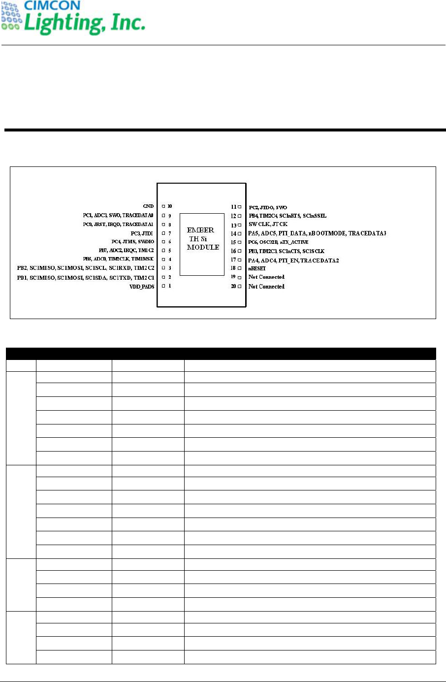
Following is the pin out of CIMCON TH Si Module with description of each pin:
Descriptions:
PIN SIGNAL
DIRECTION DESCRIPTION
1 3.3
V
Powe
r
Used to power the CIMCON RF module.
2 PB1 I/O Digital I/O
SC1MISO
O SPI slave data out of Serial Controller 1
SC1MOSI
O SPI master data out of Serial Controller 1
SC1SDA
I/O TWI data of Serial Controller 1
SC1TXD O UART transmit data of Serial Controller 1
TIM2C1
O Timer 2 channel 1 output
TIM2C1
I Timer 2 channel 1 input
3 PB2 I/O Digital I/O
SC1MISO
I SPI master data in of Serial Controller 1
SC1MOSI
I SPI slave data in of Serial Controller 1
SC1SCL
I/O TWI clock of Serial Controller 1
SC1RXD
I UART receive data of Serial Controller 1
TIM2C2 O Timer 2 channel 2 output
TIM2C2 I Timer 2 channel 2 input
4 PB5 I/O Digital I/O
A
DC0
A
nalog ADC Input 0
TIM2CLK
I Timer 2 external clock input
TIM1MSK
I Timer 1 external clock mask input
5 PB7 I/O Digital I/O
A
DC2
A
nalog ADC Input 2
IRQC I Default external interrupt source C
TIM1C2
O Timer 1 channel 2 output

Product Manual
RF Module
3-5
This information is confidential and proprietary to CSI and is to be used only for the purpose for which it is provided. Reproduction by any means,
electronic or mechanical, and distribution to third parties without express written permission from CSI is not permitted.
PIN SIGNAL
DIRECTION DESCRIPTION
TIM1C2
I Timer 1 channel 2 input
6 PC4 I/O Digital I/O
JTMS I JTAG mode select from debugger
SWDIO
I/O Serial Wire bidirectional data to/from debugger
7 PC3 I/O Digital I/O
JTDI I JTAG data in from debugger
8 PC0 I/O Digital I/O
JRST I JTAG reset input from debugger
IRQD I Default external interrupt source D
TRACEDATA1 O Synchronous CPU trace data bit 1
9 PC1 I/O Digital I/O
A
DC3
A
nalog ADC Input 3
SWO
O Serial Wire Output asynchronous trace output to
debugger
TRACEDATA0 O Synchronous CPU trace data bit 0
10 Ground Powe
r
Ground pin of RF module.
11 PC2 I/O Digital I/O
JTDO O JTAG data out to debugger
SWO
O Serial Wire Output asynchronous trace output to
debugger
12 PB4 I/O Digital I/O
TIM2C4 O Timer 2 channel 4 output
TIM2C4 I Timer 2 channel 4 input
SC1nRTS
O UART RTS handshake of Serial Controller 1
SC1nSSEL
I SPI slave select of Serial Controller 1
13 SWCL
K
I/O Serial Wire clock input/output with debugger
JTCK I JTAG clock input from debugger
14 PA5 I/O Digital I/O
A
DC5
A
nalog
A
DC Input 5
PTI_DATA O Data signal of Packet Trace Interface (PTI)
nBOOTMODE I Embedded serial bootloader activation out of reset
TRACEDATA3 O Synchronous CPU trace data bit 3
15 PC6 I/O Digital I/O
OSC32B I/O 32.768 kHz crystal oscillator
nTX_ACTIVE O Inverted TX_ACTIVE signal (see PC5)
16 PB3 I/O Digital I/O
TIM2C3 O Timer 2 channel 3 output
TIM2C3 I Timer 2 channel 3 input
SC1nCTS
I UART CTS handshake of Serial Controller 1
SC1SCLK
O SPI master clock of Serial Controller 1
SC1SCLK
I SPI slave clock of Serial Controller 1
17 PA4 I/O Digital I/O
A
DC4
A
nalog
A
DC Input 4
PTI_EN O Frame signal of Packet Trace Interface (PTI)
TRACEDATA2 O Synchronous CPU trace data bit 2
18 nReset I
A
ctive Low chip reset (Internal pull up)
19 NC N/A N/A
20 NC N/A N/A

Product Manual
RF Module
4-1
This information is confidential and proprietary to CSI and is to be used only for the purpose for which it is provided. Reproduction by any
means, electronic or mechanical, and distribution to third parties without express written permission from CSI is not permitted.
4
4
C
CO
ON
NF
FI
IG
GU
UR
RA
AT
TI
IO
ON
N
I
IN
NF
FO
OR
RM
MA
AT
TI
IO
ON
N
4.1. Absolute Maximum Ratings of RF Module
The following table provides maximum ratings of RF Module:
Sr. No. Parameter Symbol Absolute
Maximum ratings
Unit
1 Supply Voltage
V
cc -0.3 to +3.6
V
DC
2
V
oltage on any GPIO
including nReset and JCLK
V
IN -0.3 to Vcc+0.3
V
DC
3
V
oltage on any GPIO [PA4, PA5, PB5,
PB6, PB7, PC1] when used as input to
ADC
V
IN -0.3 to +2.0
V
DC
4 Storage Temperature Range Tstg -40 to +105 ‘C
5 Operating Temperature Range Top -40 to +85 ‘C
6 ESD on any pin (HBM)
V
hbm +/-2 K
V
7 ESD on RF port (CDM)
V
cdm +/-225
V
8 Moisture Sensitivity Level (MSL) MSL3
9 Reflow Temperature Treflow Refer in next pages
4.2. Recommended Operating Conditions
Sr. No Parameter Symbol Recommended Operating
Conditions
Unit
1 Supply Voltage
V
cc 2.1 to 3.6
V
DC
2 Operating frequenc
y
Fin 2405 to 24 MHz
3 Operating Temperature Top -40 to +85’C ‘C
4.3. DC Electrical Characteristics
Parameter Test Conditions Min. Typical Max
Unit
V
oltage suppl
y
2.1 3.6
V
DC
Low Schmitt switching
threshold
V
SWIL
Schmitt input
threshold going from
high to low
0.42 x
VDD_PADS
0.50 x
VDD_PADS
High Schmitt switching
threshold
V
SWIH
Schmitt input
threshold going from
low to high
0.62 x
VDD_PADS
0.80 x
VDD_PADS
V
Input current for logic 0
IIL
-0.5
uA
Input current for logic 1
IIH
+0.5
uA
Input pull-up resistor
value
RIPU
24 29 34 kΩ

Product Manual
RF Module
4-2
This information is confidential and proprietary to CSI and is to be used only for the purpose for which it is provided. Reproduction by any
means, electronic or mechanical, and distribution to third parties without express written permission from CSI is not permitted.
Parameter Test Conditions Min. Typical Max
Unit
Input pull-down resistor
value
RIPD
24
29 34 kΩ
Output voltage for logic
0
V
OL
(IOL = 4 mA for
standard pads, 8 mA
for high current
pads)
0 0.18 x
VDD_PADS
V
Output voltage for logic
1
V
OH
(IOH = 4 mA for
standard pads, 8 mA
for high current
pads)
0.82 x
VDD_PADS
V
DD_PADS
V
Output source current
(standard current pad)
IOHS
4
mA
Output sink current
(standard current pad)
IOLS
4 mA
Output source current
high current pad: PA6,
PA7, PB6, PB7, PC0
IOHH
8 mA
Output sink current
high current pad: PA6,
PA7, PB6, PB7, PC0
IOLH
8 mA
Total output current (for
I/O Pads)
IOH + IOL
40 mA
4.4. Power Settings for Regulatory Compliance
Because of the high gain of the frontend module output power of up to 24dBm can be achieved
When the antenna gain is included then the output power of the EM357 transceivers needs to be
reduced for regulatory compliance. The following tables list the maximum permitted power
setting for the different antenna types listed. This is the power out of the EM357 chip, and the
power delivered to the antenna will be higher by the gain of the PA.
settxpower P (set the channel power)
UFL Antenna Unit
• Channel 11: P = -5 [dBm]
• Channel 18: P = -5 [dBm]
• Channel 25: P = -7 [dBm]
Fixed Antenna Unit
• Channel 11: P = -3 [dBm]
• Channel 18: P = -3 [dBm]
• Channel 25: P = -3 [dBm]

Product Manual
RF Module
5-1
This information is confidential and proprietary to CSI and is to be used only for the purpose for which it is provided. Reproduction by any means,
electronic or mechanical, and distribution to third parties without express written permission from CSI is not permitted.
5
5
B
BO
OA
AR
RD
D
L
LA
AY
YO
OU
UT
T
CIMCON RF modules do not have any specific sensitivity to nearby processors, crystals or other
PCB components. Other than mechanical considerations, no special PCB placement is required for
integrating CIMCON RF radios. In general, Power and GND traces should be thicker than signal
traces and be able to comfortably support the maximum currents.
The radios are also designed to be self-sufficient and work with wire whip and external antennas
without the need for additional ground planes on the host PCB. However, considerations should be
taken on the choice of antenna and antenna location. Metal objects that are near an antenna cause
reflections and may reduce the ability for an antenna to efficiently radiate. Using an integral
antenna (like a wire whip antenna) in an enclosed metal box will greatly reduce the range of a radio.
For this type of application an external antenna would be a better choice. External antennas should
be positioned away from metal objects as much as possible. Metal objects next to the antenna or
between transmitting and receiving antennas can often block or reduce the transmission distance.
Some objects that are often overlooked are metal poles, metal studs or beams in structures, concrete
(it is usually reinforced with metal rods), metal enclosures, vehicles, elevators, ventilation ducts,
refrigerators and microwave ovens.
The Wire Whip Antenna should be straight and perpendicular to the ground plane and/or chassis.
It should reside above or away from any metal objects like batteries, tall electrolytic capacitors or
metal enclosures. If the antenna is bent to fit into a tight space, it should be bent so that as much of
the antenna as possible is away from metal. Caution should be used when bending the antenna,
since this will weaken the solder joint where the antenna connects to the module. Antenna elements
radiate perpendicular to the direction they point. Thus a vertical antenna emits across the horizon
Product Manual
RF Module
6-1
This information is confidential and proprietary to CSI and is to be used only for the purpose for which it is provided. Reproduction by any means,
electronic or mechanical, and distribution to third parties without express written permission from CSI is not permitted.
6
6
S
SO
OL
LD
DE
ER
RI
IN
NG
G
T
TE
EM
MP
PE
ER
RA
AT
TU
UR
RE
E
P
PR
RO
OF
FI
IL
LE
E
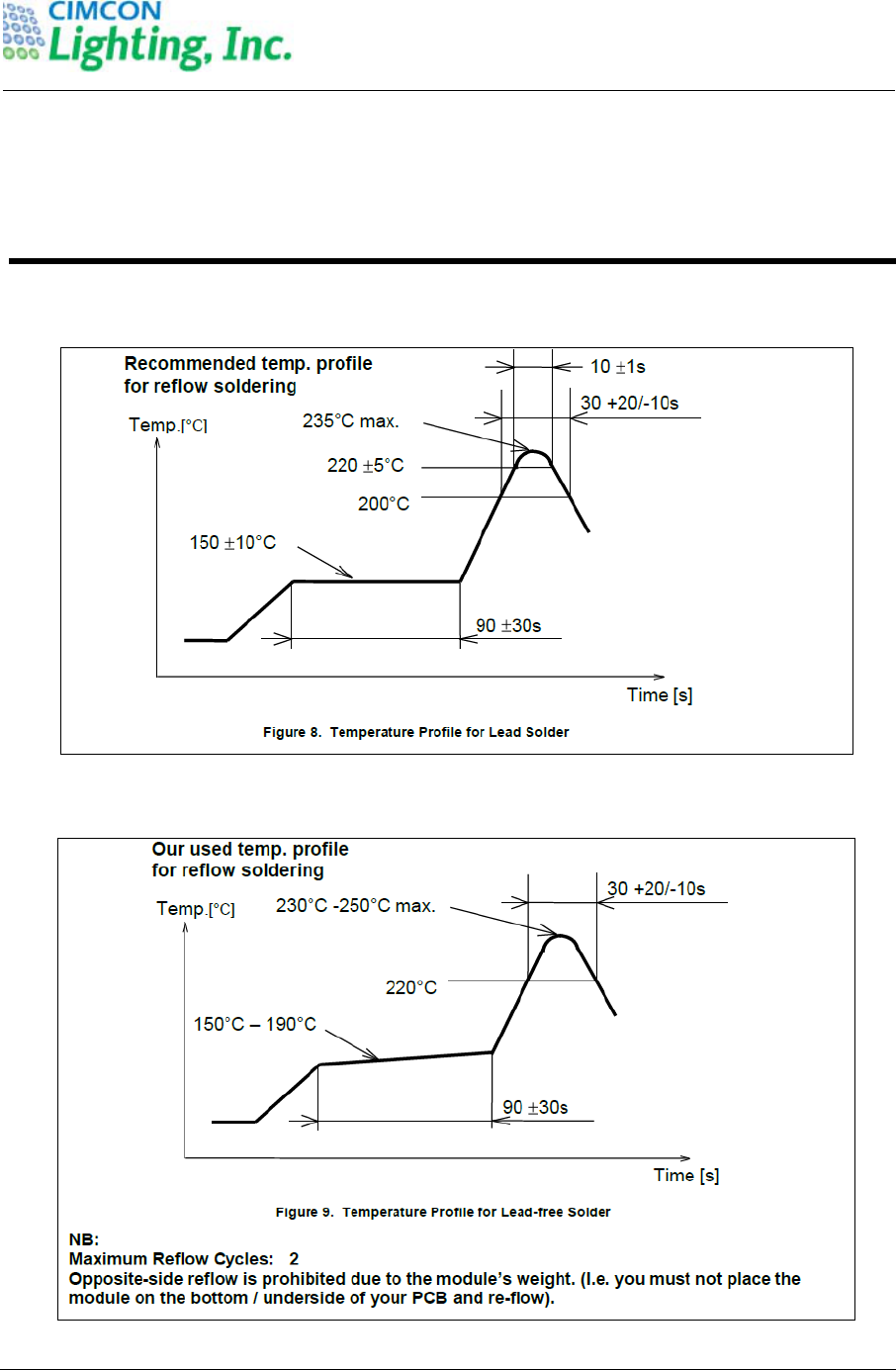
6.1. Leaded Process
6.2. Lead Free Process
Product Manual
RF Module
7-1
This information is confidential and proprietary to CSI and is to be used only for the purpose for which it is provided. Reproduction by any means,
electronic or mechanical, and distribution to third parties without express written permission from CSI is not permitted.
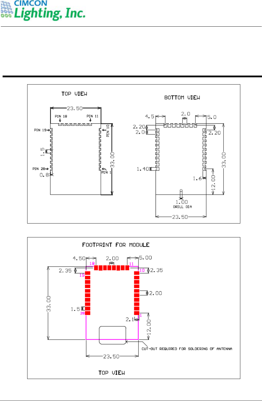
7
7
M
ME
EC
CH
HA
AN
NI
IC
CA
AL
L
D
DI
IM
ME
EN
NS
SI
IO
ON
NS
S
O
OF
F
T
TH
HE
E
S
SM
MT
T
M
MO
OD
DU
UL
LE
ES
S
Product Manual
RF Module
8-1
This information is confidential and proprietary to CSI and is to be used only for the purpose for which it is provided. Reproduction by any means,
electronic or mechanical, and distribution to third parties without express written permission from CSI is not permitted.
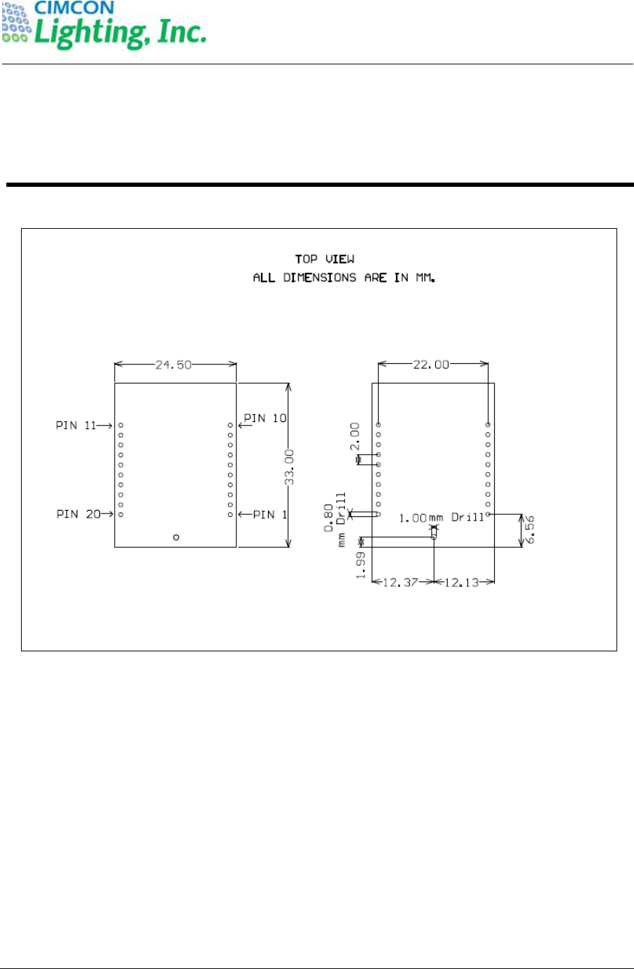
8
8
M
ME
EC
CH
HA
AN
NI
IC
CA
AL
L
D
DI
IM
ME
EN
NS
SI
IO
ON
NS
S
F
FO
OR
R
T
TH
HR
RO
OU
UG
GH
H
H
HO
OL
LE
E
M
MO
OD
DU
UL
LE
E