COBAN ELECTRONICS CB900 GSM Module User Manual CB 900 GSM GPRS Module
Shenzhen Coban Electronics Co., Ltd. GSM Module CB 900 GSM GPRS Module
User manual

CB900 GSM/GPRS Module
Product Technical Specifications
Date
:
2013-9-11
Document Version
:
1.1
Our Reference
:
02000B33

CONTENTS
1. Introduction ....................................................................................................................... 3
1.1. Abbreviations ......................................................................................................... 3
1.2. Safety Precautions ................................................................................................... 4
2. Technical Specifications ..................................................................................................... 5
2.1. General Specifications ............................................................................................. 5
2.2. GSM/ GPRS Specifications ..................................................................................... 5
2.3. RF Frequencies ....................................................................................................... 6
2.4. Baseband Functionalities ......................................................................................... 6
2.5. Interface Specifications ........................................................................................... 6
3. Functional Architecture ...................................................................................................... 7
4. INTERFACES ................................................................................................................... 8
4.1. Pin Assignments...................................................................................................... 8
4.2. Pin description ........................................................................................................ 9
4.3. Power Supply and Ground ..................................................................................... 11
4.4. Operating Modes................................................................................................... 12
4.5. Analog to Digital Converter (ADC) ....................................................................... 13
4.6. Power ON Control ................................................................................................ 13
4.7. Subscriber Identity Module (SIM) Interface ........................................................... 14
4.8. Serial Link (UART) Interfaces ............................................................................... 15
4.9. USB Interface ....................................................................................................... 17
4.10. Analog Audio Interfaces .................................................................................... 18
4.10.1. Microphone input ...................................................................................... 18
4.10.2. Speaker ..................................................................................................... 19
4.10.3. Earphone ................................................................................................... 20
4.11. General Purposes Input / Output ports .................................................................... 21
4.12. Keyboard Interface ............................................................................................ 21
4.13. 2-Wire Serial Interface ...................................................................................... 22
4.14. RF interface ...................................................................................................... 22
4.14.1. RF Performance ......................................................................................... 22
4.14.2. Recommendations...................................................................................... 22

1. Introduction
This document describes the hardware interface, including interface specifications, electrical and
mechanical details, of the CB900 module that connects to the cellular device application.
1.1. Abbreviations
The following abbreviations are used in this document:
Abbreviation
Description
ACM
Accumulated Call Meter
ADC
Analog Digital Convertor
AMR
Adaptive Multi-rate
AMR- FR
AMR Full-rate
ADN
Abbreviated Dialing Number
APN
Access Point Name
CLIP
Calling Line Identity Presentation
CSD
Circuit Switched Data
DCD
Data Carrier Detect
DCE
Data Communication Equipment
DCS
Data Coding Scheme
DTE
Data Terminal Equipment
DTMF
Dual Tone Multi Frequency
DTR
Data Terminal Ready
EFR
Enhanced Full-rate
FR
Full-rate
GPIO
General Purpose Input Output
GPRS
General Packet Radio Service
GSM
Global Standard for Mobile Communications
IP
Internet Protocol
PDP
Packet Data Protocol
PDU
Packet Data Unit
PPP
Point-to-Point Protocol
RF
Radio Frequency
RTS
Ready To Send
SIM
Subscriber Identification Number
SMS
Short Messages Service
TCP
Transmission Control Protocol
UART
Universal Asynchronous Receiver Transmitter
UDP
User Data Protocol
USSD
Unstructured Supplementary Service Data

1.2. Safety Precautions
For your own safety, please follow the safety precautions listed below during all phases of the
operation, usage, service or repair of any cellular terminal or mobile incorporating the CB900
Module. All manufacturers of these cellular terminals or mobile devices are advised to include the
following safety precautions into all manuals provided with their terminal or mobile device, and
pass this information to device users and operating personnel. Failure to comply may be
dangerous or illegal.
Road safety
Do not use a mobile device while driving. Park the vehicle first or use a hand free earphone. It is
illegal in some countries to use a mobile device while driving.
Switch off in aircraft
Cellular terminal or mobile devices can cause interference to aircraft electronics. Using them on
aircraft is both illegal and dangerous.
Switch off when refueling vehicle
Do not use the cellular terminal or mobile device at a refueling station or near fuels or chemicals.
Forbidden Usage
Always switch off your cellular terminal or mobile device where it is forbidden to be used in any
areas like a hospital.
Interference
All cellular terminals or mobile devices may be subjected to radio interference, which could affect
their performance.
Emergency calls
As the GSM/GPRS module is based on GSM standard for radio signals and cellular networks, this
connection cannot be guaranteed at all times under all conditions. It should never be entirely relied
upon for essential communications such as an emergency call.
Note on compliance with international rules and regulations
The CB900 module is a fully certified cellular radio engine. The module has been tested and
certified for compliance to international safety and GSM standard requirements at the modular
level.
Manufacturers of cellular terminal or mobile equipment incorporating the CB900 are required to
test their final products to ensure compliance to these EMC tests/requirements:
ESD
Radiated Spurious Emissions
Conducted Emissions, if applicable
Further tests if applicable
The module was not assessed against the essential requirement ‘health’. Manufacturers of the final
products are also responsible to ensure that their products are tested for compliance to any other
health requirements that might be applicable.
A few other important notes regarding safety in implementation and usage of the module:
The module shall be supplied by a Limited Power Supply (LPS) according to EN60950:2000.
No necessary spacing (creepage and clearance distance) shall be reduced by installing the
module into the final equipment.
Provisions shall be made for fastening the module securely in the end product.
Instructions and equipment markings related to safety shall be in a language, which is acceptable
in the country in which the equipment is to be installed.
2. Technical Specifications
2.1. General Specifications
Feature
Description
Network Type
Quad-Band GSM/GPRS
Frequency Bands
Quad Band: GSM850 / EGSM900 / DCS1800 / PCS1900
Output Power
GSM 850 / EGSM 900 : Class 4 (2W)
DCS1800 / PCS1900: Class 1 (1W)
Physical Dimensions
Dimensions: 27.3 *27.3 *3mm
Weight: 5g (including of shielding)
Power Supply
3.5V to 4.6V
Operational
Environmental Description
Normal Operating
Temperature
-20° C to +55° C
Extended Operating
Temperature
-40° C to +85° C
Relative humidity
5 – 95%
2.2. GSM/ GPRS Specifications
Feature
Description
GSM Audio
Telephony
Emergency call
Half Rate, Full Rate and Enhanced Full Rate (HR/FR/EFR)
Adaptive Multi-rate (AMR)
Hands-Free Operation
Echo Cancellation (Enhanced AEC)
Noise Reduction
DTMF (encoding only)
SMS
Point-to-point (MO/MT)
Cell Broadcast
Text and PDU mode
GPRS
Class 12/10/8
Mobile Station Class B
Coding Schemes MCS1 – MCS4
TCP Stack, UDP Stack
HTTP Stack, FTP Stack
PPP Stack
2.3. RF Frequencies
RF functionalities comply with the GSM Phase II GSM 850/EGSM 900/DCS 1800/PCS 1900
recommendations.
The frequencies covered are:
Tx GSM850: (824 ~ 849 MHz)
Tx EGSM900: (880 ~ 915 MHz)
Tx DCS1800: (1710 ~ 1785 MHz)
Tx PCS1900: (1850 ~ 1910 MHz)
Rx GSM850: (869 ~ 894 MHz)
Rx EGSM900: (925 ~ 960 MHz)
Rx DCS1800: (1805 ~ 1880 MHz)
Rx PCS1900: (1930 ~ 1990 MHz)
2.4. Baseband Functionalities
The Baseband is composed of an ARM, The digital baseband power supply is 1.2V and the digital
IO power supply is 1.8V.
2.5. Interface Specifications
Feature
Description
68-pin LCC
Power Supply
Back-up Battery
Keypad
2 Serial Link UART
USB 1.1
1.8V/3V SIM
Real time clock
GPIOs
Analog to Digital Converter
Analog Audio
Reset
Power On
Battery Charging Interface
I2C master*
*For hardware reference only. These features are not enabled in the standard module firmware as
it requires a certain level of firmware customization depending on its intended application. Please
contact COBAN for more information
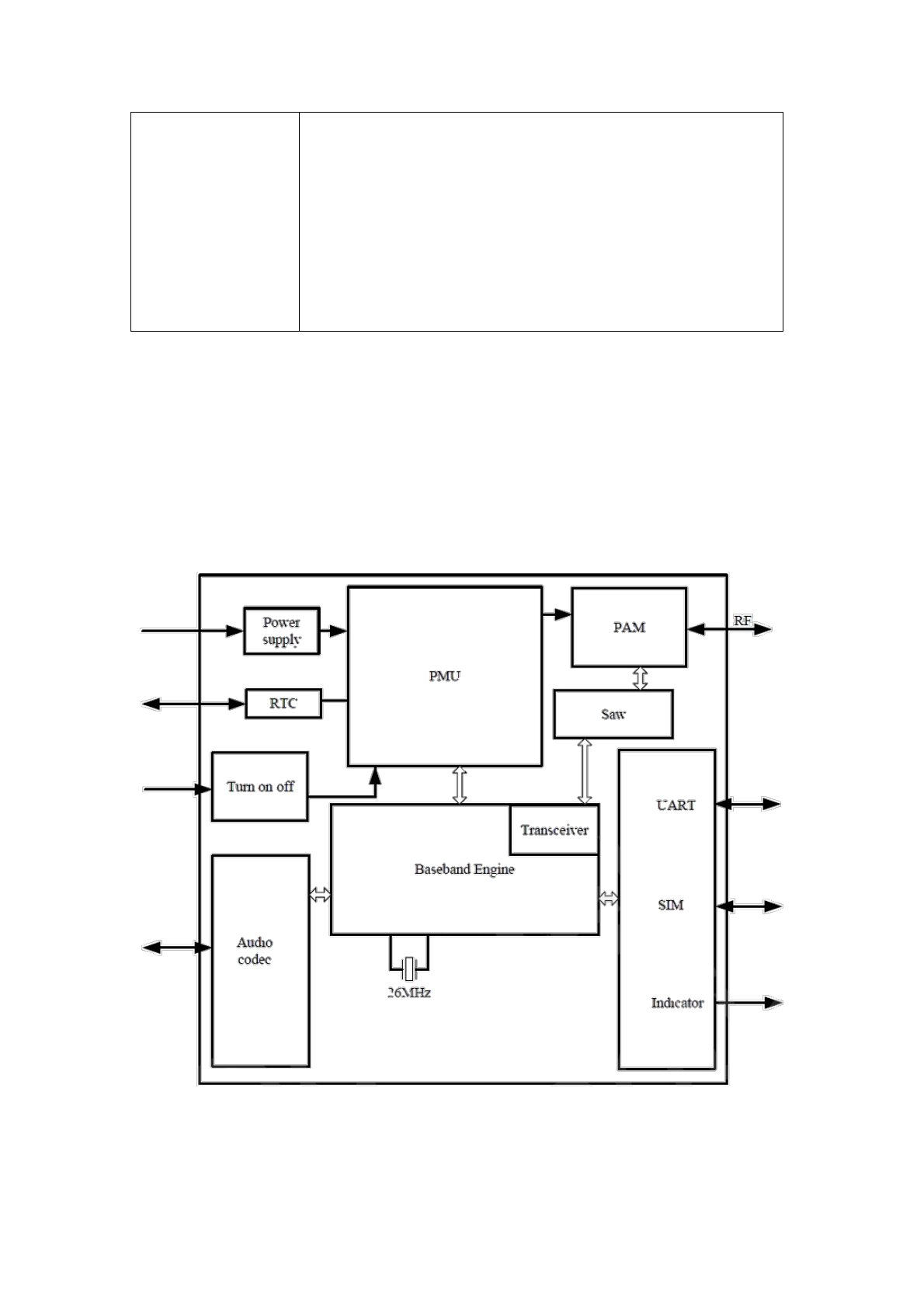
3. Functional Architecture
Figure 1 shows a block diagram of CB900 module and illustrate the major functional components
Figure 1: CB900 Functional Architecture Block Diagram
4. INTERFACES
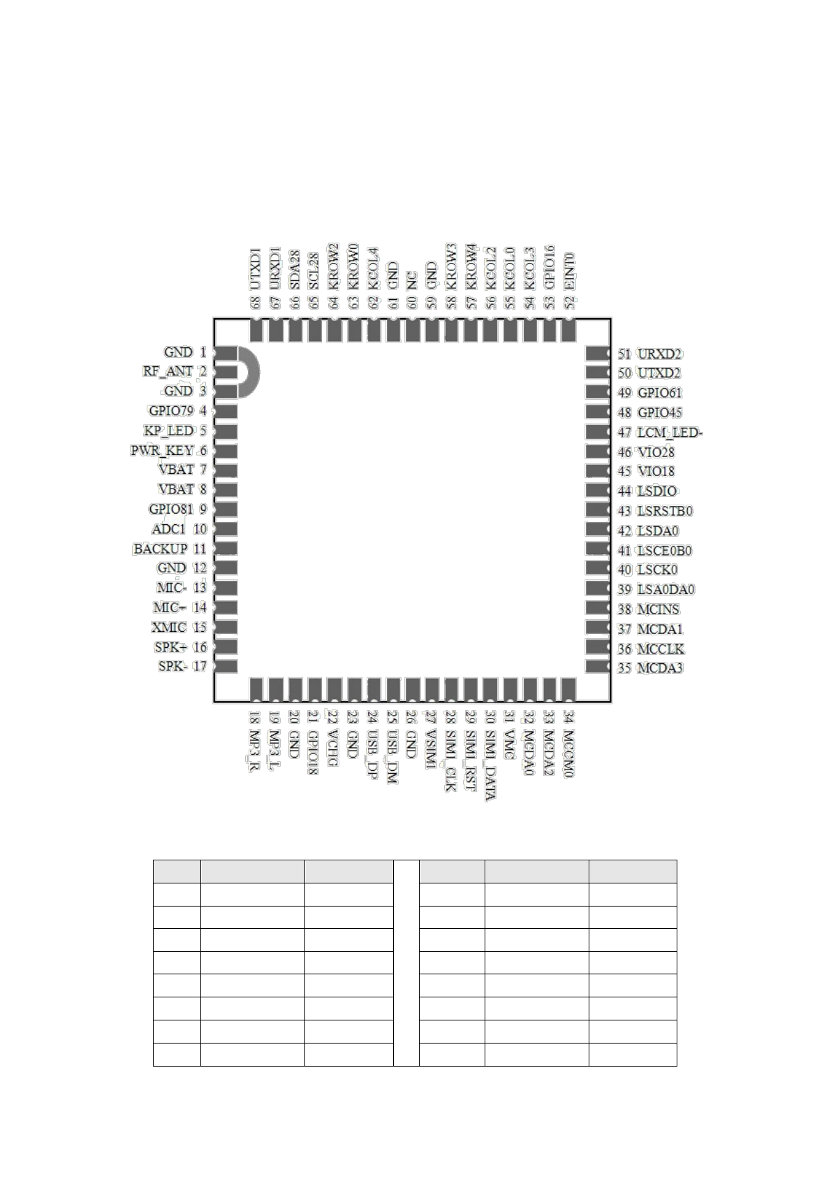
4.1. Pin Assignments
Figure 2: CB900 Pin assignments
Pin
Signal Name
Signal I/O
Pin
Signal Name
Signal I/O
1
GND
35
MCDA3
I/O
2
RF_ANT
I/O
36
MCCLK
I/O
3
GND
37
MCDA1
I/O
4
GPIO79
I/O
38
MCINS
I/O
5
KP_LED
I/O
39
LSA0DA0
I/O
6
PWR_KEY
I
40
LSCK0
I/O
7
VBAT
I
41
LSCE0B0
I/O
8
VBAT
I
42
LSDA0
I/O
4.2. Pin description
9
GPIO81
I/O
43
LSRSTB0
I
10
ADC1
I
44
LSDIO
I/O
11
BACKUP
I/O
45
VIO18
O
12
GND
46
VIO28
O
13
MIC-
I
47
LCM_LED-
O
14
MIC+
I
48
GPIO45
I/O
15
XMIC
I
49
GPIO61
I/O
16
SPK+
O
50
UTXD2
O
17
SPK-
O
51
URXD2
I
18
MP3_R
O
52
EINT0
I
19
MP3_L
O
53
GPIO16
I/O
20
GND
54
KCOL3
I/O
21
GPIO18
I/O
55
KCOL0
I/O
22
VCHG
I
56
KCOL2
I/O
23
GND
57
KROW4
I/O
24
USB_DP
I/O
58
KROW3
I/O
25
USB_DM
I/O
59
GND
26
GND
60
NC
27
VSIM1
O
61
GND
28
SIM1_CLK
O
62
KCOL4
I/O
29
SIM1_RST
O
63
KROW0
I/O
30
SIM1_DATA
I/O
64
KROW2
I/O
31
VMC
O
65
SCL28
I/O
32
MCDA0
I/O
66
SDA28
I/O
33
MCDA2
I/O
67
URXD1
I
34
MCCM0
I/O
68
UTXD1
O
Pin
Signal Name
Signal I/O
Description
Remark
1
GND
2
RF_ANT
I/O
RF I / O 50 ohm characteristic impedance
3
GND
4
GPIO79
I/O
General Purpose IO
Not to float
5
KP_LED
I/O
Keyboard backlight
Not to float
6
PWR_KEY
I
Low PWR_KEY for a specified time
period to boot or shutdown
Internally
pulled up to
2.8V
7
VBAT
I
I
VBAT=3.5V~4.6V
Maximum
load current
8
VBAT

2A
9
GPIO81
I/O
General Purpose IO
Not to float
10
ADC1
I
Analog to digital conversion
Not to float
11
BACKUP
I/O
Backup battery pin
Not to float
12
GND
13
MIC-
I
Audio Input channel 1
Not to float
14
MIC+
15
XMIC
I
Audio Input channel 2
16
SPK+
O
Audio Output channel 1
17
SPK-
18
MP3_R
O
Audio Output channel 2
19
MP3_L
20
GND
21
GPIO18
I/O
General Purpose IO
Not to float
22
VCHG
I
Charging Pin
Not to float
23
GND
24
USB_DP
I/O
USB data cable positive signal
Not to float
25
USB_DM
I/O
USB data cable negative signal
Not to float
26
GND
27
VSIM1
O
SIM card supply voltage
SIM card
into the
module line
should not
exceed 20cm
28
SIM1_CLK
O
SIM card clock line
29
SIM1_RST
O
SIM card reset line
30
SIM1_DATA
I/O
SIM card data cable
31
VMC
O
SD card power cable
Not to float
32
MCDA0
I/O
SD card data cable
Not to float
33
MCDA2
I/O
SD card data cable
Not to float
34
MCCM0
I/O
SD card command line
Not to float
35
MCDA3
I/O
SD card data cable
Not to float
36
MCCLK
I/O
SD card clock line
Not to float
37
MCDA1
I/O
SD card data cable
Not to float
38
MCINS
I/O
SD card insertion detection line
Not to float
39
LSA0DA0
I/O
LCD address line
Not to float
40
LSCK0
I/O
LCD clock line
Not to float
41
LSCE0B0
I/O
LCD chip select line
Not to float
42
LSDA0
I/O
LCD data address line
Not to float
43
LSRSTB0
I
LCD reset line
Not to float
44
LSDIO
I/O
LCD data cable
Not to float
45
VIO18
O
LCD power
Not to float
46
VIO28
O
47
LCM_LED-
O
LCD backlight
Not to float
48
GPIO45
I/O
General Purpose IO
Not to float
4.3. Power Supply and Ground
The power supply design is one of the key design areas for a GSM terminal due to the burst
characteristics of GSM transmission. The supply must be able to deliver very high current peaks in
a very short time during a GSM transmit burst, typically up to 2A. During these bursts, it is
recommended that the voltage drop does not exceed 400mV. The voltage ripple should not exceed
50mV at frequencies up to 200 kHz and 2mV at frequencies above 200 kHz. This might cause the
module to reset.
All four legs of the shield must be soldered onto the target PCB. The ground connection of
the target PCB has to go through a full ground plane on the PCB.
Power Supply Voltage
The power supply voltage for VBATT is given below:
49
GPIO61
I/O
General Purpose IO
Not to float
50
UTXD2
O
Serial data transmit
Not to float
51
URXD2
I
Serial data receive
Not to float
52
EINT0
I
External interrupt input
Not to float
53
GPIO16
I/O
General Purpose IO
Not to float
54
KCOL3
I
Keyboard input
Not to float
55
KCOL0
I
Keyboard input
Not to float
56
KCOL2
I
Keyboard input
Not to float
57
KROW4
I
Keyboard input
Not to float
58
KROW3
I
Keyboard input
Not to float
59
GND
60
NC
61
GND
62
KCOL4
I
Keyboard input
Not to float
63
KROW0
I
Keyboard input
Not to float
64
KROW2
I
Keyboard input
Not to float
65
SCL28
I/O
I2C clock line
Not to float
66
SDA28
I/O
I2C data cable
Not to float
67
URXD1
I
Serial data receive
Not to float
68
UTXD1
O
Serial data transmit
Not to float
Power Supply
Parameters
Conditions
Min
Type
Max
Unit
VBAT
Supply Voltages
Voltage measured at the VBAT pin. If
voltage drops below 3.5V, the module
will automatically power off.
3.5*
4.2
4.6
V
Voltage Drop
Normal condition with max transmitter
output
400
mV
Note: * must be guaranteed to ensure compliance with the GSM certification requirements.
Figure 3: voltage and current waveform of the modules at launch
Figure 4: VBAT input reference circuit
4.4. Operating Modes
Operation Type
Mode
Description
Normal
Operation
GSM IDLE
The module is registered to the network. Power
consumption depends on the interval of the network
paging.
GSM CONNECTED
The module has established a call connection with the
network. Power consumption depends on the network
settings and coverage
Voltage Ripple
Normal condition with max transmitter
output
50
mV
GPRS IDLE
The module is attached to the GPRS network. Power
consumption depends on the network settings.
GPRS DATA
The module sends and receives data from the network.
Power consumption depends on the network settings
and GPRS configurations.
Reduced
operation
GSM SLEEP
In order to extend the battery life of hand held
devices, the module can enter into a sleep mode with
software command. The module will wake up from
the sleep mode if there are any activities.
AIRPLANE
The module disconnect from the network just like
SLEEP but keep the SIM active so that activity like
accessing the phone book in SIM is still possible.
Battery Charging
CHARGE
The module performs battery charging in parallel with
other operation
4.5. Analog to Digital Converter (ADC)
Electrical Characteristics
Figure 5: ADC input reference circuit
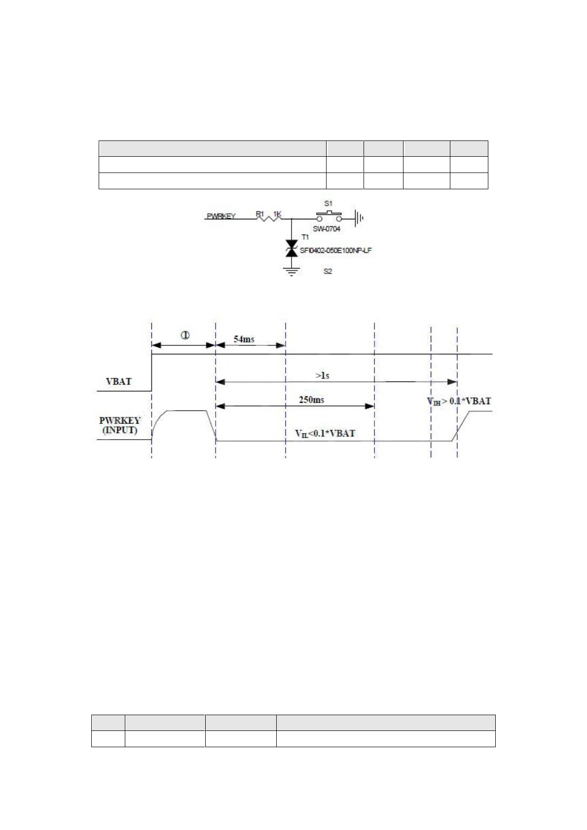
4.6. Power ON Control
This input pin is used to switch the module ON. A switch-ON interruption is triggered in the
module at the detection of a falling edge of this signal pin over a period of 250ms.
Note: The module should be properly switched OFF before all power supplies are removed. This
is to avoid any unforeseen corruption of internal data.
Parameters
Conditions
Min
Type
Max
Unit
Resolution
-
-
10
-
Bits
Reference voltage
-
-
2.8
-
V
Differential non-linearity
-
-2
-
2
LSB
Integral non-linearity
Best Fitting
-2
-
2
LSB
Input Range
-
0
2.8
V
Input Resistance
-
1
100
KΩ
Pin Description
Electrical Characteristics
Figure 6: KEY Power ON reference circuit
Boot timing diagram is as following:
Figure 7: Boot timing diagram
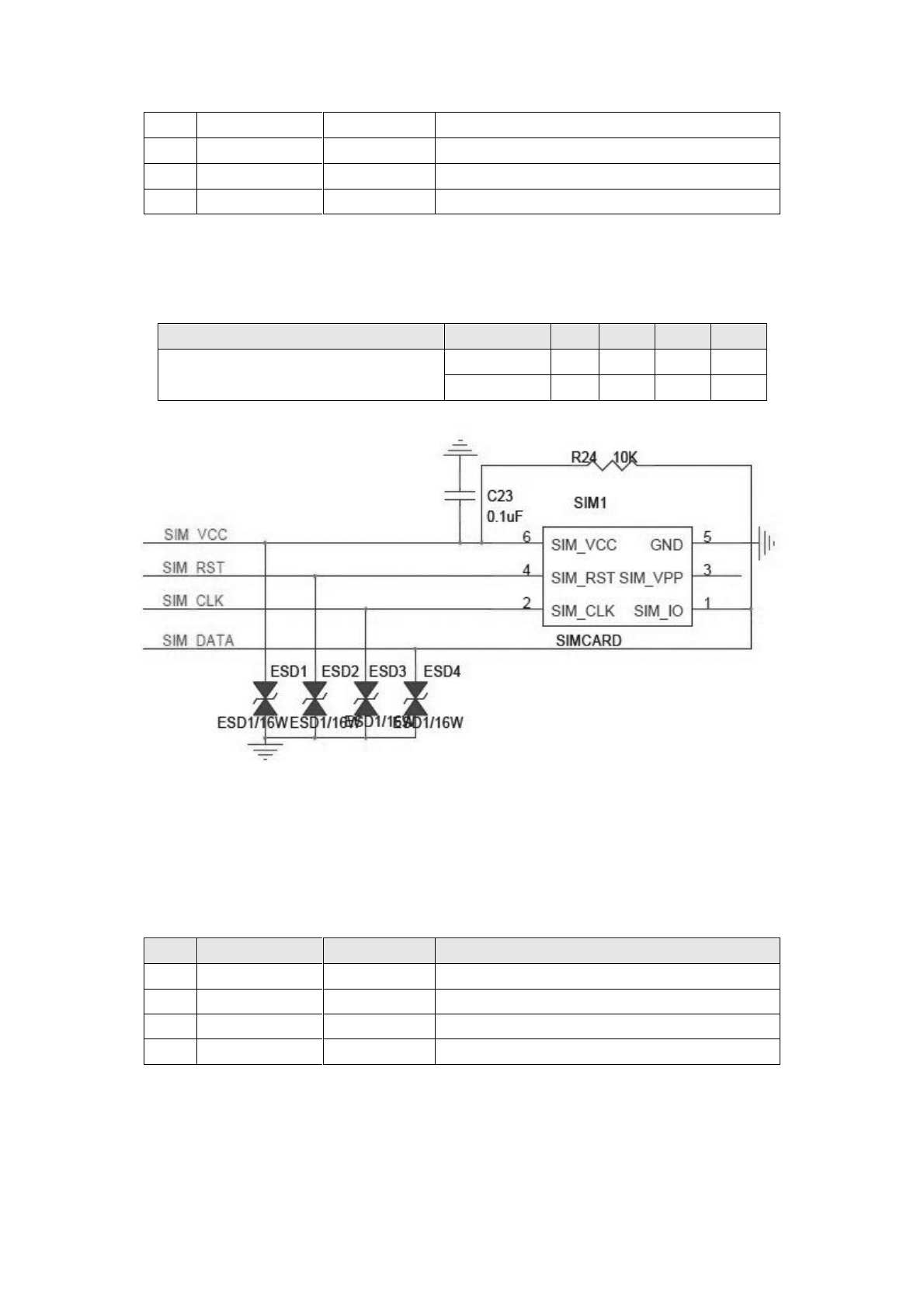
4.7. Subscriber Identity Module (SIM) Interface
The SIM card interface is composed of an internally dedicated voltage regulator and I/O level
shifters. It is able to support both 1.8V and 3V SIM cards. It is recommended that the routing
traces of the SIM interface lines be kept as short as possible. ESD diodes can be added to the
signals connected to the SIM socket to prevent any ESD-related issues. The diodes shall be placed
as close to the SIM socket as possible. Also, a decoupling capacitor of about 100nF should be
added on the VSIM1 line near the SIM socket. At any point of time, only one SIM card is to be
connected as the same pins of both (SIM holder placed on top of the module, external SIM holder)
are shorted.
Pin Description
Parameters
Min
Type
Max
Unit
High level input voltage, VIH
2
-
-
V
Low level input voltage, VIL
-
-
-0.805
V
Pin
Signal Name
Signal I/O
Description
27
VSIM1
O
SIM card supply voltage, the module
Electrical Characteristics
Figure 8: Example of a SIM socket implementation
4.8. Serial Link (UART) Interfaces
The module has two UART. Baud rate from 300 bits/s up to 115200 bits/s feature.
Note: Default factory setting baudrate is set at 115200, unless other specified.
Application
The block diagram below shows the possible UART connection.
automatically selects 1.8v or 3.0v
28
SIM1_CLK
O
SIM card clock line
29
SIM1_RST
O
SIM card reset line
30
SIM1_DATA
I/O
SIM card data cable
Parameters
Conditions
Min
Type
Max
Unit
VSIM1
SIM 3V
2.7
2.85
2.95
V
SIM 1.8V
1.65
1.8
1.95
V
Pin
Signal Name
Signal I/O
Description
50
UTXD2
O
DCE Data Transmit
51
URXD2
I
DCE Data Receive
67
URXD1
I
DCE Debug serial Data Receive
68
UTXD1
O
DCE Debug serial Data Transmit
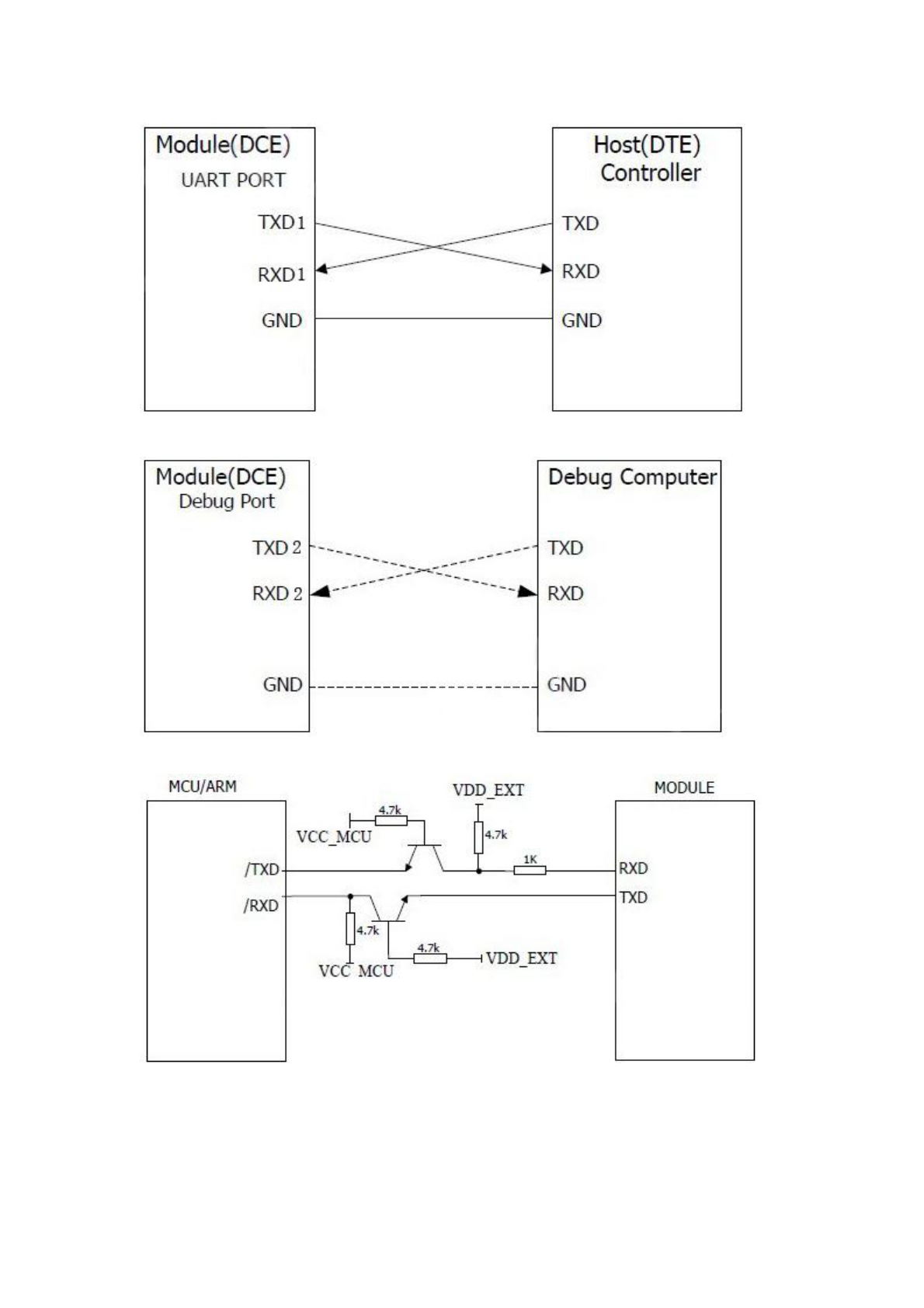
Figure 9: Interfacing with UART
Figure 10: Interfacing with UART
Figure 11: Level-shifter connection to 5V level
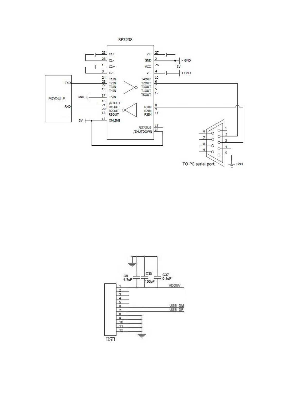
Figure 12: Level-shifter connection to RS232
4.9. USB Interface
The USB interface supports a USB 1.1. It is primarily intended for flashing of firmware and for
use as command and data interface.
Application
Note: Connection of a 4.7F Capacitor externally at VBUS for filtering is required.
Figure 13: Example of USB implementation
4.10. Analog Audio Interfaces
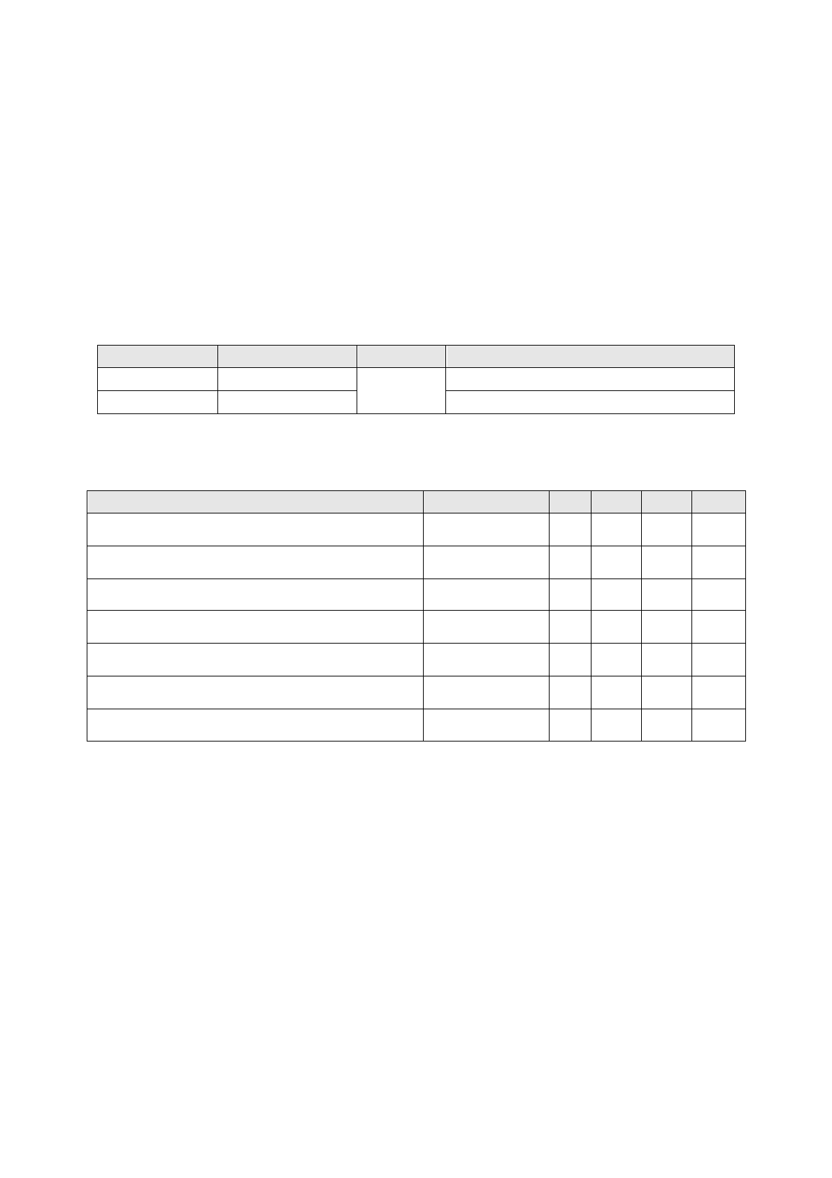
4.10.1. Microphone input
The handset differential inputs MICIP and MICIN can be amplified by the differential handset
microphone amplifier. The microphone reference voltage is at 2V.
Pin Description
Electrical Characteristics
MIC Application
This section describes the two common approaches to microphone connection. Since this feature
is exposed to the environment, provision for ESD protection is recommended. Typical
characteristics of a microphone device which can be used: Impedance: ~2 kohm, sensitivity ~
40-50 dB/PA and SNR >50 dB.
Differential Ended
Differential ended connection is the recommended implementation. The following diagram shows
a proposed implementation. The capacitance values chosen may need to be optimized based on
application, for GSM related EMI, this can be from 10 pF to 47 pF for an 0402 size. If not needed,
these components may be unplaced.
Pin
Signal Name
Signal I/O
Description
13
MIC-
I
Microphone amplifier input (-ve)
14
MIC+
Microphone amplifier input (+ve)
Parameters
Conditions
Min
Type
Max
Unit
Maximum differential input range (MIC+ – MIC-)
Input 3 dBm0
-
-
0.8
Vpp
Nominal reference level (MIC+ – MIC-)
-
-
-10
-
dBm
Differential input resistance (MIC+ – MIC-)
-
-
50
-
KΩ
Amplifier gain for (MICIP-MICIN) input
Differential MIC
-
-
39
dB
Recommended MIC Impedance
-
2k
-
Ohms
Recommended MIC Sensitivity
40
-
50
dB/PA
Recommended MIC SNR
-
-
50
dB
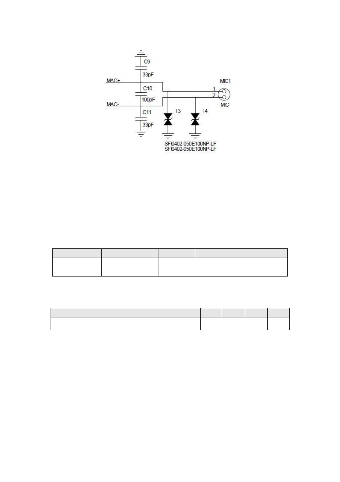
Figure 14: Example of Microphone implementation
4.10.2. Speaker
The class D amplifier is capable of driving 700 mWrms into an 8 ohms load. Default switching
frequency is 600 kHz.
Pin Description
Electrical Characteristics
Application
The connections to the speaker should run in parallel to the transducer and provisions for shunt
capacitors are recommended for filtering RF and Digital Noise. Suggested values are 33 pF for
EMI. Ensure that the voltage rating of the selected components can withstand operation at the
maximum swing voltages in both directions, 16 volt parts should be sufficient. Since this feature is
exposed to the environment, provision for ESD protection is recommended.
Pin
Signal Name
Signal I/O
Description
16
SPK+
O
Speaker signal (+ve)
17
SPK-
Speaker signal (-ve)
Parameters
Min
Type
Max
Unit
Output Load Resistance
-
8
-
Ω
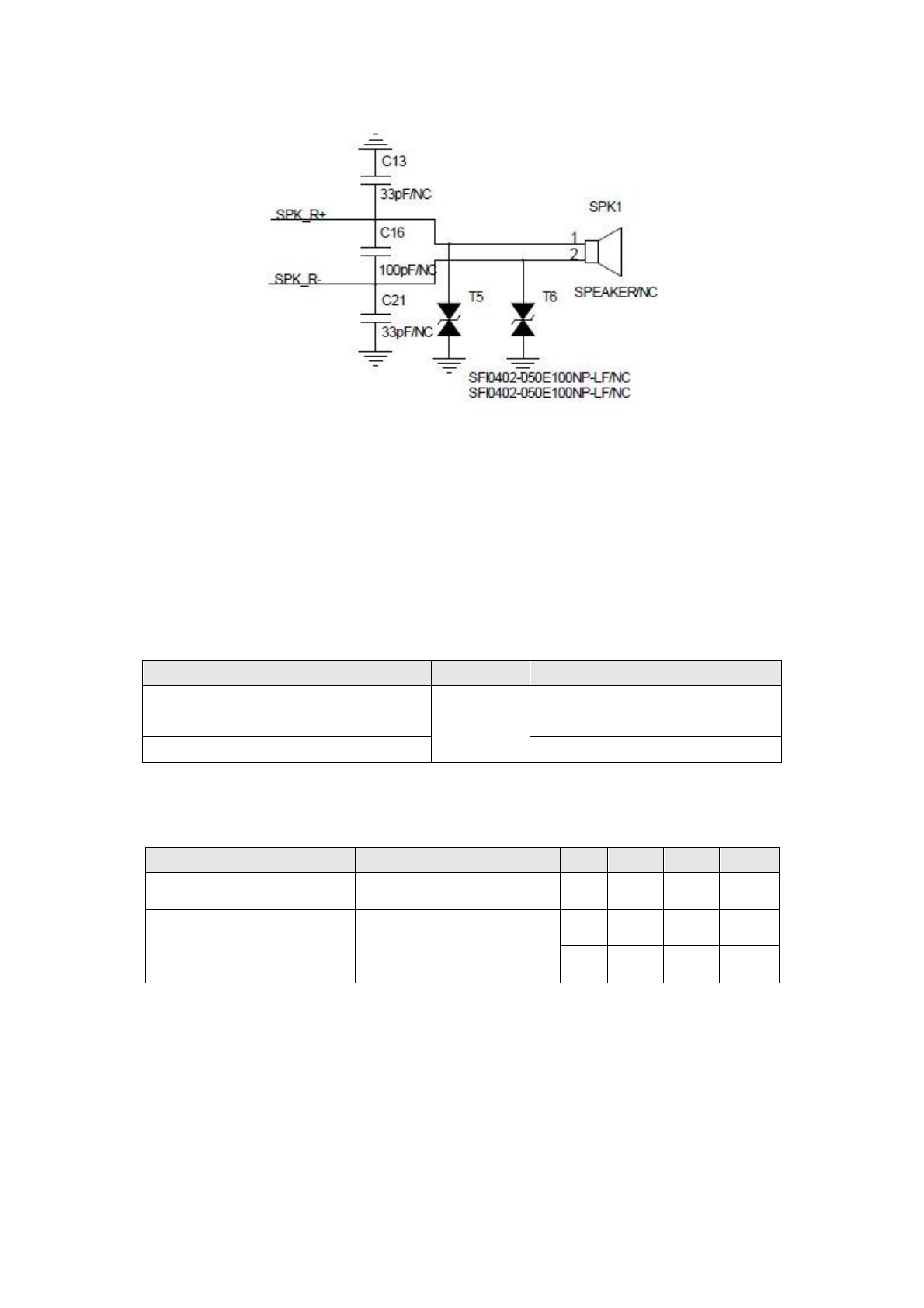
Figure 15: Example of speaker implementation
4.10.3. Earphone
The earphone amplifier provides a full differential signal on the MP3_R and MP3_L
terminals. The amplifier is capable of driving 100 mWrms into a 16 ohm load.
Pin Description
Electrical Characteristics
Pin
Signal Name
Signal I/O
Description
15
XMIC
I
Earphone input
18
MP3_R
O
Earphone amplifier output (+ve)
19
MP3_L
Earphone amplifier output (-ve)
Parameters
Conditions
Min
Type
Max
Unit
Power supply rejection
Mono Modes(GSM Voice)
90
100
-
dB
Maximum Output Swing at
EARP-EARN
Load = OPEN
-
-
4.1
Vpp
Figure 15: Example of earphone implementation
4.11. General Purposes Input / Output ports
Pin Description and Electrical Characteristics
4.12. Keyboard Interface
The 10-pin keyboard interface includes 4 row inputs and 4 column outputs. The 8 lines can
be used as general purpose inputs and outputs. Please contact COBAN directly for more
information on the extended customization to this interface.
Pin Description and Electrical Characteristics
Pin
Signal Name
Parameters
Min
Type
Max
Unit
4
9
21
48
49
53
GPIO79
GPIO81
GPIO18
GPIO45
GPIO61
GPIO16
High level input voltage, VIH
2.5
3
V
Low level input voltage, VIL
0
0.3
V
High level output voltage, VOH
2.6
2.8
2.85
V
Low level output voltage, VOL
-
-
0.45
V
Pin
Signal Name
Parameters
Min
Type
Max
Unit
54
55
56
KCOL3
KCOL0
KCOL2
High level input voltage, VIH
2.5
3
V
Low level input voltage, VIL
0
0.3
V
4.13. 2-Wire Serial Interface
This is a half-duplex serial port using 2-line for data transmission consisting of SDA data signal
and SDL clock signal. It can transfer at speeds up to 400Kbits/s (fast-mode).
Note: Supports 1.8V I2C compliant devices.
Pin Description and Electrical Characteristics
This feature is not enabled in the standard module firmware as it requires a certain level of
firmware customization depending on its intended application. Please contact COBAN for more
information.
4.14. RF interface
CB900 RF interface has a characteristic impedance of 50. The matching networks for an
external antenna connection are not included in the module and should be placed on the
application board.
4.14.1. RF Performance
4.14.2. Recommendations
The antenna must fulfill the following requirements below:
57
58
62
63
64
KROW4
KROW3
KCOL4
KROW0
KROW2
High level output voltage, VOH
2.6
2.8
2.85
V
Low level output voltage, VOL
-
-
0.45
V
Pin
Signal Name
Parameters
Min
Type
Max
Unit
65
66
SCL28
SDA28
High level input voltage (SDA and SCL), VIH
-
-
2.8
V
Low level input voltage(SDA and SCL), VIL
0
-
-
V
Frequency Bands
RF Sensitivity (dBm) (Nominal)
GSM 850/EGSM 900
-106dBm
DCS1800/ PCS1900
-104dBm
Frequency Bands
EGSM 900
DCS 1800
GSM 850
PCS 1900

The optimum operating frequency depends on the application. A dual-band or a quad band
antenna must operate in the above frequency bands.
TX Frequency
880 - 915 MHz
1710 - 1785 MHz
824 - 849 MHz
1850 - 1910 MHz
RX Frequency
925 - 960 MHz
1805 - 1880 MHz
869 - 894 MHz
1930 - 1990 MHz
Impedance
50 ohm
VSWR Rx max
1.5 : 1
VSWR Tx max
1.5 : 1
Typical radiated gain
0 dBi in one direction at least

FCC Caution.
§ 15.19 Labelling requirements.
This device complies with part 15 of the FCC Rules. Operation is subject to the following two
conditions: (1) This device may not cause harmful interference, and (2) this device must accept
any interference received, including interference that may cause undesired operation.
§ 15.21 Changes or modification warning
Any Changes or modifications not expressly approved by the party responsible for compliance
could void the user's authority to operate the equipment.
§ 15.105 Information to the user.
Note: This equipment has been tested and found to comply with the limits for a Class B digital
device, pursuant to part 15 of the FCC Rules. These limits are designed to provide reasonable
protection against harmful interference in a residential installation. This equipment generates
uses and can radiate radio frequency energy and, if not installed and used in accordance with the
instructions, may cause harmful interference to radio communications. However, there is no
guarantee that interference will not occur in a particular installation. If this equipment does
cause harmful interference to radio or television reception, which can be determined by turning
the equipment off and on, the user is encouraged to try to correct the interference by one or
more of the following measures:
-Reorient or relocate the receiving antenna.
-Increase the separation between theequipment and receiver.
-Connect the equipment into an outlet on a circuit different from that to which the receiver is
connected.
-Consult the dealer or an experienced radio/TV technician for help.
* RF warning for Portable device:
The device has been evaluated to meet general RF exposure requirement. The device can be used
in portable exposure condition without restriction.
The GSM module is designed to comply with the FCCstatement. FCC ID is 2AA64CB900. The host
system using GSM module, should have label indicated FCC ID :2AA64CB900