CalAmp Wireless Networks 2424046-001 T-96SR UHF Telemetry Transceiver/Modem User Manual Cover dmf
CalAmp Wireless Networks Corporation T-96SR UHF Telemetry Transceiver/Modem Cover dmf
Contents
- 1. Transceiver Manual
- 2. Modem Manual
Transceiver Manual

SYNTHESIZED UHF TELEMETRY UNIT
PART NO. 242-3412-XX0
Second Printing
August 1997
Supersedes 001-3412-001 December 1996
Part No. 001-3412-002 8-97 Printed in U.S.A.

SYNTHESIZED UHF TELEMETRY UNIT
PART NO. 242-3412-XYZ
Copyright 1997 by the Johnson Data Telemetry Corporation.
The Johnson Data Telemetry Corporation designs and manufactures radios and radio modems to serve a wide variety of data
communication needs. The Johnson Data Telemetry Corporation produces equipment for the fixed data market including
SCADA systems for utilities, petrochemical, waste and fresh water management markets and RF boards for OEM applications
in the Radio Frequency Data Capture market. In addition, the Johnson Data Telemetry Corporation provides wireless commu-
nication solutions to the mobile data market serving public safety, utilities and industrial users.
DATA TELEMETRY PRODUCT WARRANTY
The manufacturer's warranty statement for this product is available from your product supplier or from the Johnson Data
Telemetry Corporation, 299 Johnson Avenue, PO Box 1733, Waseca, MN 56093-0833. Phone (507) 835-8819.
WARNING
This device complies with Part 15 of the FCC rules and Industry Canada RSS-119, issue 5. Operation is subject to the condi-
tion that this device does not cause harmful interference. In addition, changes or modification to this equipment not expressly
approved by the Johnson Data Telemetry Corporation could void the user's authority to operate this equipment (FCC rules,
47CFR Part 15.19).
DO NOT allow the antenna to come close to or touch, the eyes, face, or any exposed body parts while the radio is transmitting.
DO NOT operate the radio near electrical blasting caps or in an explosive atmosphere.
DO NOT operate the radio unless all the radio frequency connectors are secure and any open connectors are properly termi-
nated.
DO NOT allow children to operate transmitter equipped radio equipment.
SAFETY INFORMATION
Proper operation of this radio will result in user exposure below the Occupational Safety and Health Act and Federal Commu-
nication Commission limits.
The information in this document is subject to change without notice.
™ Johnson Data Telemetry is a trademark of the Johnson Data Telemetry Corporation.
™ RNET is a trademark of Motorola Inc.

1
TABLE OF CONTENTS
1 GENERAL INFORMATION
1.1 SCOPE OF MANUAL . . . . . . . . . . . . . . . . . . . . . . . . . . . . . . . . . . . . . . . . . . . . . . . . . . . . . . . . . . . . . . . . . . . . . . . 1-1
1.2 EQUIPMENT DESCRIPTION. . . . . . . . . . . . . . . . . . . . . . . . . . . . . . . . . . . . . . . . . . . . . . . . . . . . . . . . . . . . . . . . 1-1
GENERAL . . . . . . . . . . . . . . . . . . . . . . . . . . . . . . . . . . . . . . . . . . . . . . . . . . . . . . . . . . . . . . . . . . . . . . . . . . . . . . . . . 1-1
DL-3412 WITH LOADER BOARD . . . . . . . . . . . . . . . . . . . . . . . . . . . . . . . . . . . . . . . . . . . . . . . . . . . . . . . . . . . . . 1-1
DL-3412 WITH RNET™ MODEM . . . . . . . . . . . . . . . . . . . . . . . . . . . . . . . . . . . . . . . . . . . . . . . . . . . . . . . . . . . . . 1-2
DL3412 WITH DL3296 MODEM. . . . . . . . . . . . . . . . . . . . . . . . . . . . . . . . . . . . . . . . . . . . . . . . . . . . . . . . . . . . . . . 1-2
DM-3412 SYNTHESIZER PROGRAMMING. . . . . . . . . . . . . . . . . . . . . . . . . . . . . . . . . . . . . . . . . . . . . . . . . . . . . 1-2
1.3 TRANSCEIVER IDENTIFICATION . . . . . . . . . . . . . . . . . . . . . . . . . . . . . . . . . . . . . . . . . . . . . . . . . . . . . . . . . . 1-2
1.4 ACCESSORIES . . . . . . . . . . . . . . . . . . . . . . . . . . . . . . . . . . . . . . . . . . . . . . . . . . . . . . . . . . . . . . . . . . . . . . . . . . . . 1-2
1.5 PART NUMBER BREAKDOWN . . . . . . . . . . . . . . . . . . . . . . . . . . . . . . . . . . . . . . . . . . . . . . . . . . . . . . . . . . . . . 1-3
1.6 FACTORY CUSTOMER SERVICE . . . . . . . . . . . . . . . . . . . . . . . . . . . . . . . . . . . . . . . . . . . . . . . . . . . . . . . . . . . 1-3
1.7 PRODUCT WARRANTY . . . . . . . . . . . . . . . . . . . . . . . . . . . . . . . . . . . . . . . . . . . . . . . . . . . . . . . . . . . . . . . . . . . . 1-3
1.8 REPLACEMENT PARTS. . . . . . . . . . . . . . . . . . . . . . . . . . . . . . . . . . . . . . . . . . . . . . . . . . . . . . . . . . . . . . . . . . . . 1-3
1.9 FACTORY RETURNS . . . . . . . . . . . . . . . . . . . . . . . . . . . . . . . . . . . . . . . . . . . . . . . . . . . . . . . . . . . . . . . . . . . . . . 1-4
2 INSTALLATION
2.1 PRE-INSTALLATION CHECKS . . . . . . . . . . . . . . . . . . . . . . . . . . . . . . . . . . . . . . . . . . . . . . . . . . . . . . . . . . . . . 2-1
2.2 INTERFACING WITH DATA EQUIPMENT . . . . . . . . . . . . . . . . . . . . . . . . . . . . . . . . . . . . . . . . . . . . . . . . . . . 2-1
DM3412 (RF Board) . . . . . . . . . . . . . . . . . . . . . . . . . . . . . . . . . . . . . . . . . . . . . . . . . . . . . . . . . . . . . . . . . . . . . . . . . 2-1
3 PROGRAMMING
3.1 INTRODUCTION . . . . . . . . . . . . . . . . . . . . . . . . . . . . . . . . . . . . . . . . . . . . . . . . . . . . . . . . . . . . . . . . . . . . . . . . . . 3-1
3.2 SYNTHESIZER DATA PROTOCOL . . . . . . . . . . . . . . . . . . . . . . . . . . . . . . . . . . . . . . . . . . . . . . . . . . . . . . . . . . 3-1
GENERAL . . . . . . . . . . . . . . . . . . . . . . . . . . . . . . . . . . . . . . . . . . . . . . . . . . . . . . . . . . . . . . . . . . . . . . . . . . . . . . . . . 3-1
D-WORD CALCULATION (24-BITS). . . . . . . . . . . . . . . . . . . . . . . . . . . . . . . . . . . . . . . . . . . . . . . . . . . . . . . . . . . 3-2
C-WORD CALCULATION (24-BITS). . . . . . . . . . . . . . . . . . . . . . . . . . . . . . . . . . . . . . . . . . . . . . . . . . . . . . . . . . . 3-2
B-WORD CALCULATION (24-BITS). . . . . . . . . . . . . . . . . . . . . . . . . . . . . . . . . . . . . . . . . . . . . . . . . . . . . . . . . . . 3-3
A0-WORD CALCULATION (24-BITS). . . . . . . . . . . . . . . . . . . . . . . . . . . . . . . . . . . . . . . . . . . . . . . . . . . . . . . . . . 3-4
3.3 RECEIVE TO TRANSMIT SEQUENCE . . . . . . . . . . . . . . . . . . . . . . . . . . . . . . . . . . . . . . . . . . . . . . . . . . . . . . . 3-6
3.4 TRANSMIT TO RECEIVE SEQUENCE . . . . . . . . . . . . . . . . . . . . . . . . . . . . . . . . . . . . . . . . . . . . . . . . . . . . . . . 3-6
3.5 RADIO DIAGNOSTICS . . . . . . . . . . . . . . . . . . . . . . . . . . . . . . . . . . . . . . . . . . . . . . . . . . . . . . . . . . . . . . . . . . . . . 3-7
4 CIRCUIT DESCRIPTION
4.1 GENERAL . . . . . . . . . . . . . . . . . . . . . . . . . . . . . . . . . . . . . . . . . . . . . . . . . . . . . . . . . . . . . . . . . . . . . . . . . . . . . . . . 4-1
INTRODUCTION . . . . . . . . . . . . . . . . . . . . . . . . . . . . . . . . . . . . . . . . . . . . . . . . . . . . . . . . . . . . . . . . . . . . . . . . . . . 4-1
SYNTHESIZER . . . . . . . . . . . . . . . . . . . . . . . . . . . . . . . . . . . . . . . . . . . . . . . . . . . . . . . . . . . . . . . . . . . . . . . . . . . . . 4-1
RECEIVER. . . . . . . . . . . . . . . . . . . . . . . . . . . . . . . . . . . . . . . . . . . . . . . . . . . . . . . . . . . . . . . . . . . . . . . . . . . . . . . . . 4-1
TRANSMITTER . . . . . . . . . . . . . . . . . . . . . . . . . . . . . . . . . . . . . . . . . . . . . . . . . . . . . . . . . . . . . . . . . . . . . . . . . . . . 4-1
LOADER BOARD. . . . . . . . . . . . . . . . . . . . . . . . . . . . . . . . . . . . . . . . . . . . . . . . . . . . . . . . . . . . . . . . . . . . . . . . . . . 4-1
4.2 SYNTHESIZER . . . . . . . . . . . . . . . . . . . . . . . . . . . . . . . . . . . . . . . . . . . . . . . . . . . . . . . . . . . . . . . . . . . . . . . . . . . . 4-1
VOLTAGE-CONTROLLED OSCILLATOR . . . . . . . . . . . . . . . . . . . . . . . . . . . . . . . . . . . . . . . . . . . . . . . . . . . . . . 4-3
VCO AND REFERENCE OSCILLATOR MODULATION . . . . . . . . . . . . . . . . . . . . . . . . . . . . . . . . . . . . . . . . . . 4-4
CASCODE AMPLIFIERS/VCO (Q851/Q852). . . . . . . . . . . . . . . . . . . . . . . . . . . . . . . . . . . . . . . . . . . . . . . . . . . . . 4-4
AMPLIFIER (Q853) . . . . . . . . . . . . . . . . . . . . . . . . . . . . . . . . . . . . . . . . . . . . . . . . . . . . . . . . . . . . . . . . . . . . . . . . . 4-4
VOLTAGE FILTER (Q901) . . . . . . . . . . . . . . . . . . . . . . . . . . . . . . . . . . . . . . . . . . . . . . . . . . . . . . . . . . . . . . . . . . . 4-4
VCO FREQUENCY SHIFT (Q841) . . . . . . . . . . . . . . . . . . . . . . . . . . . . . . . . . . . . . . . . . . . . . . . . . . . . . . . . . . . . . 4-4
SYNTHESIZER IC (U811) . . . . . . . . . . . . . . . . . . . . . . . . . . . . . . . . . . . . . . . . . . . . . . . . . . . . . . . . . . . . . . . . . . . . 4-5
LOCK DETECT. . . . . . . . . . . . . . . . . . . . . . . . . . . . . . . . . . . . . . . . . . . . . . . . . . . . . . . . . . . . . . . . . . . . . . . . . . . . . 4-5

2
TABLE OF CONTENTS
4.3 RECEIVER CIRCUIT DESCRIPTION . . . . . . . . . . . . . . . . . . . . . . . . . . . . . . . . . . . . . . . . . . . . . . . . . . . . . . . . 4-5
HELICAL FILTER (Z201), RF AMPLIFIER (Q201) . . . . . . . . . . . . . . . . . . . . . . . . . . . . . . . . . . . . . . . . . . . . . . . 4-5
MIXER (U211). . . . . . . . . . . . . . . . . . . . . . . . . . . . . . . . . . . . . . . . . . . . . . . . . . . . . . . . . . . . . . . . . . . . . . . . . . . . . 4-6
FIRST LO AMPLIFIER (Q301). . . . . . . . . . . . . . . . . . . . . . . . . . . . . . . . . . . . . . . . . . . . . . . . . . . . . . . . . . . . . . . . 4-6
BUFFER (Q211), CRYSTAL FILTER (Z221/Z222), IF AMP (Q231). . . . . . . . . . . . . . . . . . . . . . . . . . . . . . . . . . 4-6
SECOND LO AMP/TRIPLER (Q401). . . . . . . . . . . . . . . . . . . . . . . . . . . . . . . . . . . . . . . . . . . . . . . . . . . . . . . . . . . 4-6
SECOND MIXER/DETECTOR (U241) . . . . . . . . . . . . . . . . . . . . . . . . . . . . . . . . . . . . . . . . . . . . . . . . . . . . . . . . . 4-6
4.4 TRANSMITTER CIRCUIT DESCRIPTION . . . . . . . . . . . . . . . . . . . . . . . . . . . . . . . . . . . . . . . . . . . . . . . . . . . . 4-7
BUFFER (Q501). . . . . . . . . . . . . . . . . . . . . . . . . . . . . . . . . . . . . . . . . . . . . . . . . . . . . . . . . . . . . . . . . . . . . . . . . . . . 4-7
PRE-DRIVER (Q511) . . . . . . . . . . . . . . . . . . . . . . . . . . . . . . . . . . . . . . . . . . . . . . . . . . . . . . . . . . . . . . . . . . . . . . . 4-7
FINAL (U521), COMPARATOR (U111C) . . . . . . . . . . . . . . . . . . . . . . . . . . . . . . . . . . . . . . . . . . . . . . . . . . . . . . . 4-7
ANTENNA SWITCH (CR561, CR562). . . . . . . . . . . . . . . . . . . . . . . . . . . . . . . . . . . . . . . . . . . . . . . . . . . . . . . . . . 4-8
TRANSMIT KEY-UP CONTROL. . . . . . . . . . . . . . . . . . . . . . . . . . . . . . . . . . . . . . . . . . . . . . . . . . . . . . . . . . . . . . 4-8
4.5 VOLTAGE REGULATORS . . . . . . . . . . . . . . . . . . . . . . . . . . . . . . . . . . . . . . . . . . . . . . . . . . . . . . . . . . . . . . . . . . 4-8
+9.6 AND +5.5V REGULATED . . . . . . . . . . . . . . . . . . . . . . . . . . . . . . . . . . . . . . . . . . . . . . . . . . . . . . . . . . . . . . . 4-8
5 SERVICING
5.1 GENERAL. . . . . . . . . . . . . . . . . . . . . . . . . . . . . . . . . . . . . . . . . . . . . . . . . . . . . . . . . . . . . . . . . . . . . . . . . . . . . . . . . 5-1
PERIODIC CHECKS . . . . . . . . . . . . . . . . . . . . . . . . . . . . . . . . . . . . . . . . . . . . . . . . . . . . . . . . . . . . . . . . . . . . . . . . 5-1
SURFACE-MOUNTED COMPONENTS. . . . . . . . . . . . . . . . . . . . . . . . . . . . . . . . . . . . . . . . . . . . . . . . . . . . . . . . 5-1
SCHEMATIC DIAGRAMS AND COMPONENT LAYOUTS . . . . . . . . . . . . . . . . . . . . . . . . . . . . . . . . . . . . . . . 5-1
REPLACEMENT PARTS LIST. . . . . . . . . . . . . . . . . . . . . . . . . . . . . . . . . . . . . . . . . . . . . . . . . . . . . . . . . . . . . . . . 5-1
TCXO MODULE NOT SERVICEABLE . . . . . . . . . . . . . . . . . . . . . . . . . . . . . . . . . . . . . . . . . . . . . . . . . . . . . . . . 5-1
5.2 SYNTHESIZER SERVICING . . . . . . . . . . . . . . . . . . . . . . . . . . . . . . . . . . . . . . . . . . . . . . . . . . . . . . . . . . . . . . . .5-1
INTRODUCTION . . . . . . . . . . . . . . . . . . . . . . . . . . . . . . . . . . . . . . . . . . . . . . . . . . . . . . . . . . . . . . . . . . . . . . . . . . 5-1
REFERENCE OSCILLATOR . . . . . . . . . . . . . . . . . . . . . . . . . . . . . . . . . . . . . . . . . . . . . . . . . . . . . . . . . . . . . . . . . 5-1
VCO . . . . . . . . . . . . . . . . . . . . . . . . . . . . . . . . . . . . . . . . . . . . . . . . . . . . . . . . . . . . . . . . . . . . . . . . . . . . . . . . . . . . . 5-1
SYNTHESIZER (U801). . . . . . . . . . . . . . . . . . . . . . . . . . . . . . . . . . . . . . . . . . . . . . . . . . . . . . . . . . . . . . . . . . . . . . 5-2
5.3 RECEIVER SERVICING . . . . . . . . . . . . . . . . . . . . . . . . . . . . . . . . . . . . . . . . . . . . . . . . . . . . . . . . . . . . . . . . . . . . 5-2
SUPPLY VOLTAGES AND CURRENT . . . . . . . . . . . . . . . . . . . . . . . . . . . . . . . . . . . . . . . . . . . . . . . . . . . . . . . . 5-2
MIXER/DETECTOR (U241) . . . . . . . . . . . . . . . . . . . . . . . . . . . . . . . . . . . . . . . . . . . . . . . . . . . . . . . . . . . . . . . . . . 5-2
SECOND LO (Q401) . . . . . . . . . . . . . . . . . . . . . . . . . . . . . . . . . . . . . . . . . . . . . . . . . . . . . . . . . . . . . . . . . . . . . . . . 5-3
AUDIO BUFFER AMP (U261) . . . . . . . . . . . . . . . . . . . . . . . . . . . . . . . . . . . . . . . . . . . . . . . . . . . . . . . . . . . . . . . . 5-3
IF AMP (U231). . . . . . . . . . . . . . . . . . . . . . . . . . . . . . . . . . . . . . . . . . . . . . . . . . . . . . . . . . . . . . . . . . . . . . . . . . . . . 5-3
BUFFER AMP (Q211), CRYSTAL FILTERS . . . . . . . . . . . . . . . . . . . . . . . . . . . . . . . . . . . . . . . . . . . . . . . . . . . . 5-3
MIXER (U211). . . . . . . . . . . . . . . . . . . . . . . . . . . . . . . . . . . . . . . . . . . . . . . . . . . . . . . . . . . . . . . . . . . . . . . . . . . . . 5-3
LNA (Q202), HELICAL FILTERS . . . . . . . . . . . . . . . . . . . . . . . . . . . . . . . . . . . . . . . . . . . . . . . . . . . . . . . . . . . . . 5-3
ANTENNA SWITCH. . . . . . . . . . . . . . . . . . . . . . . . . . . . . . . . . . . . . . . . . . . . . . . . . . . . . . . . . . . . . . . . . . . . . . . . 5-3
5.4 TRANSMITTER SERVICING . . . . . . . . . . . . . . . . . . . . . . . . . . . . . . . . . . . . . . . . . . . . . . . . . . . . . . . . . . . . . . . . 5-3
SUPPLY VOLTAGES AND CURRENT . . . . . . . . . . . . . . . . . . . . . . . . . . . . . . . . . . . . . . . . . . . . . . . . . . . . . . . . 5-3
VCO (A801) . . . . . . . . . . . . . . . . . . . . . . . . . . . . . . . . . . . . . . . . . . . . . . . . . . . . . . . . . . . . . . . . . . . . . . . . . . . . . . . 5-3
PRE-DRIVER (Q511) . . . . . . . . . . . . . . . . . . . . . . . . . . . . . . . . . . . . . . . . . . . . . . . . . . . . . . . . . . . . . . . . . . . . . . . 5-3
FINAL AMPLIFIER (U521) . . . . . . . . . . . . . . . . . . . . . . . . . . . . . . . . . . . . . . . . . . . . . . . . . . . . . . . . . . . . . . . . . . 5-4
ANTENNA SWITCH (CR561/CR562) . . . . . . . . . . . . . . . . . . . . . . . . . . . . . . . . . . . . . . . . . . . . . . . . . . . . . . . . . . 5-4
MODULATION INPUT (J201, PIN 6) . . . . . . . . . . . . . . . . . . . . . . . . . . . . . . . . . . . . . . . . . . . . . . . . . . . . . . . . . . 5-4
TCXO (Y801). . . . . . . . . . . . . . . . . . . . . . . . . . . . . . . . . . . . . . . . . . . . . . . . . . . . . . . . . . . . . . . . . . . . . . . . . . . . . . 5-4

3
TABLE OF CONTENTS
6 ALIGNMENT PROCEDURE AND PERFORMANCE TESTS
6.1 GENERAL . . . . . . . . . . . . . . . . . . . . . . . . . . . . . . . . . . . . . . . . . . . . . . . . . . . . . . . . . . . . . . . . . . . . . . . . . . . . . . . . 6-1
6.2 TEST EQUIPMENT . . . . . . . . . . . . . . . . . . . . . . . . . . . . . . . . . . . . . . . . . . . . . . . . . . . . . . . . . . . . . . . . . . . . . . . . 6-1
6.3 DL3412 TRANSCEIVER ONLY . . . . . . . . . . . . . . . . . . . . . . . . . . . . . . . . . . . . . . . . . . . . . . . . . . . . . . . . . . . . . . 6-1
VCO CONTROL VOLTAGE . . . . . . . . . . . . . . . . . . . . . . . . . . . . . . . . . . . . . . . . . . . . . . . . . . . . . . . . . . . . . . . . . . 6-1
TRANSMITTER AND FREQUENCY ALIGNMENT (OEM Not Using Diagnostics). . . . . . . . . . . . . . . . . . . . . . 6-1
MODULATION ALIGNMENT . . . . . . . . . . . . . . . . . . . . . . . . . . . . . . . . . . . . . . . . . . . . . . . . . . . . . . . . . . . . . . . . 6-2
TRANSMITTER AND FREQUENCY ALIGNMENT (Johnson Loader Using Diagnostics) . . . . . . . . . . . . . . . . . 6-2
MODULATION ADJUSTMENT . . . . . . . . . . . . . . . . . . . . . . . . . . . . . . . . . . . . . . . . . . . . . . . . . . . . . . . . . . . . . . . 6-2
RECEIVER ALIGNMENT . . . . . . . . . . . . . . . . . . . . . . . . . . . . . . . . . . . . . . . . . . . . . . . . . . . . . . . . . . . . . . . . . . . . 6-4
IF AND AUDIO ADJUSTMENTS . . . . . . . . . . . . . . . . . . . . . . . . . . . . . . . . . . . . . . . . . . . . . . . . . . . . . . . . . . . . . . 6-4
7 PARTS LIST
8 SCHEMATICS AND COMPONENT LAYOUTS

1-1
August 1997
Part No. 001-3412-002
SECTION 1 GENERAL INFORMATION
1.1 SCOPE OF MANUAL
This service manual contains alignment and ser-
vice information for the Johnson Data Telemetry
(JDT) DM-3412 UHF Synthesized Telemetry Unit.
This manual concentrates on the RF section of
the data link which may be paired with an internal
Loader board or 9600 baud Modem board.
Service manuals addressing items specific to the
Loader board (Part No. 001-3240-001) and the
Modem boards (Part No. 001-3276-001/001-3296-
001) should be referenced for the users specific con-
figuration.
1.2 EQUIPMENT DESCRIPTION
1.2.1 GENERAL
The JDT DM-3412 is a synthesized data trans-
ceiver (transmitter and receiver) which operates in the
380-512 MHz UHF frequency range. Transmitter
power output is 5 watts nominal at 13.3V DC in sim-
plex or half duplex modes.
Versions of the DM-3412 covered in this manual
are indicated in Section 1.5. The DM-3412 has a fre-
quency stability of ± 1.5 PPM (see Section 3) and is
available with or without the Loader/Modem boards.
The number of channels that can be selected with
the DM-3412 model is determined by the customer
supplied synthesizer loading circuitry. The
DL-3412 model is 8-Channels when supplied with the
DL-3240 Loader board, the DL-3276 modem kit or
the DL-3296 modem kit.
In addition to this UHF radio, JDT has a full line
of radios and radio modems to meet wireless data
communication needs. Both OEM RF decks and com-
plete FCC and Industry Canada type approved radios
and radio modems are available from 132-174 MHz at
VHF, 380-512 MHz at UHF and 928-960 MHz at
900 MHz in both 5W and 2W units (VHF and UHF).
High Specification units are available to meet Interna-
tional requirements and bandwidths to meet U.S.A.
refarming requirements. To learn more about the
other JDT products, call 1-800-992-7774 or 1-612-
890-8155 to speak to a sales representative.
1.2.2 DL-3412 WITH LOADER BOARD
The DL-3412 (Part No. 242-3412-xxx) can be
ordered with the 8-channel Loader board (Part No.
023-3240-001). The Loader board performs synthe-
sizer loading through an RS-232 DB-9 interface. In
addition, this board has circuitry which provides elec-
tronic control of the following:
Transmit/Receive data conditioning and gating
Carrier Detect
Power Control
Modulation Flatness
Audio/Data Filtering
Sleep/Wake-up to minimize current consumption
Diagnostics that includes:
Input Voltage Sense
Input Current Sense
Ambient Temperature Sense
RSSI Indicator (RSSI Sense)
Forward/Reverse Power Sense.
The gating circuits allow user selection of data
filtering (standard or wide band) and also pre-empha-
sis/de-emphasis to be enabled or disabled.
This board is programmed using an IBM PC or
compatible computer and the Johnson Data Telemetry
programming software. Programming information is
stored by an EEPROM on the Loader board. Refer to
Section 3.3 for programming information.
NOTE: The synthesizer must be loaded each time
power is turned on. Therefore, one loader board or
customer supplied programming circuit is required for
each data transceiver.
GENERAL INFORMATION
1-2
August 1997
Part No. 001-3412-002
1.2.3 DL-3412 WITH RNET™ MODEM
The DL-3412 (Part No. 242-3412-xxx) can be
ordered with the 9600 baud Modem (Part No. 023-
3276-001), which supports the RNET™ communica-
tion protocol. This modem allows data communica-
tion between the Johnson Data Telemetry high specifi-
cation synthesized products and the Motorola RNET
radio/modems.
The Modem features include:
lUser Programmable Data Rates:
9600/4800/2400/1200 baud in a 25 kHz bandwidth
OR
1200/2400/4800 baud in a 12.5 kHz bandwidth.
lRS-232 compatible using DE-15 15-pin connector.
lSimplex or Half-Duplex operation.
lRTS-CTS handshaking protocol with option for
configuring any two units as a digital repeater
(Half-Duplex or Simplex).
lSupports asynchronous, serial or transparent data
formats.
lFront panel LEDs provide indication for Transmit,
Receive and Power.
lBuilt-In Diagnostics reported both locally and
"Over-The-Air":
Reports specific unit programming
Loopback test feature
RSSI
Forward and Reflected Power
Temperature
Supply Voltage
l8-Channels programmable with option to switch
channels remotely "Over-The-Air".
This board is programmed using an IBM PC or
compatible computer using MS-DOS and the RSS
programming software (Part No. 023-3276-005). Pro-
gramming instructions contained in the RSS Manual
included in the part number listed in Table 1-1.
1.2.4 DL3412 WITH DL3296 MODEM
The DL3296 modem (Part No. 023-3296-001)
provides digital data transmission at data rates up to
9600 baud. The DL3296 operates in Half-Duplex
mode. However, two transceivers can be combined to
provide Full-Duplex operation. The user interface is a
serial port through a 9-pin D-connector configurable
to either RS-232 or TTL signal levels. The data for-
mat is asynchronous with either 8 or 9 data bits. The
modem can operate in either standard DTE/DCE
handshake protocol or in Data Activation mode which
requires only receive and transmit data lines. The
baud rates are user selectable from 300 to 9600 baud
in a 25 kHz bandwidth or 300 to 4800 baud in a
12.5 kHz bandwidth.
1.2.5 DM-3412 SYNTHESIZER PROGRAMMING
The DM-3412, when used without the Universal
Loader Board (Part No. 023-3240-001) or DL-3276/
DL-3296 modem kits, requires customer supplied
circuitry to load the synthesizer with channel informa-
tion. The protocol that this circuitry must follow is
described in Section 3.
1.3 TRANSCEIVER IDENTIFICATION
The transceiver identification number is printed
on a label that is affixed to the PC board. The follow-
ing information is contained in that number:
1.4 ACCESSORIES
Accessories available for the DL-3412 data trans-
ceiver are listed in Table 1-1.
Table 1-1 ACCESSORIES
Accessory Part No.
DL-3240 Loader Kit 023-3240-001
DL-3296 Modem Kit 023-3296-001
DL-3276 Modem Kit 023-3276-001
DL-3295 Telemetry Modem 250-3295-001/101
DL-3282 Modem* 250-3282-001
DL-3276 Service Manual 001-3276-001
DL-3240 Service Manual 001-3240-001
DL-3296 Service Manual 001-3296-001
Interface Cable 023-3276-007
Interface Cable 023-3276-008
* Must have Loader Kit installed in radio to make this
modem compatible with radio.
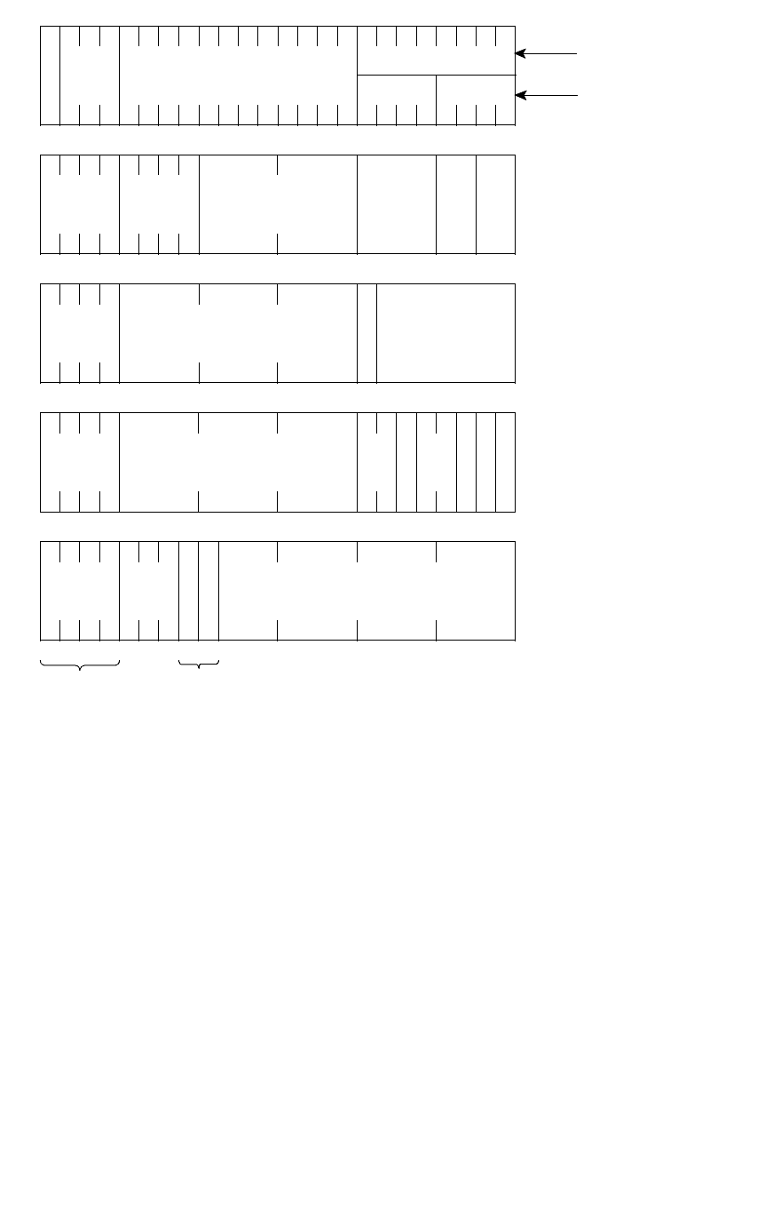
3412 2A 1 4 3 A12345
Model Revision
Letter
Ninth Digit
of PN
Manufacture
Date
Week No.
of Year Year
Plant
Warranty
Number

GENERAL INFORMATION
1-3
August 1997
Part No. 001-3412-002
1.5 PART NUMBER BREAKDOWN
The following is a breakdown of the part number
used to identify this transceiver:
1.6 FACTORY CUSTOMER SERVICE
The Customer Service Department of the
Johnson Data Telemetry Corporation provides cus-
tomer assistance on technical problems and the avail-
ability of local and factory repair facilities. Customer
Service hours are 7:30 a.m. - 4:30 p.m. Central Time,
Monday - Friday. There is also a 24-hour emergency
technical support telephone number. From within the
continental United States, the Customer Service
Department can be reached at this toll-free number
1-800-992-7774
When your call is answered at the Johnson Data
Telemetry Corporation, you will hear a brief message
informing you of numbers that can be entered to reach
various departments. This number may be entered
during or after the message using a tone-type tele-
phone. If you have a pulse-type telephone, wait until
the message is finished and an operator will come on
the line to assist you. When you enter a first number
of "3", another number is requested to further catego-
rize the type of information you need. You may also
enter the 4-digit extension number of the person that
you want to reach if you know what it is.
FAX Machine - Sales (612) 882-5671
FAX Machine - Cust Serv (507) 835-6969
If you are calling from outside the continental
United States, the Customer Service telephone num-
bers are as follows:
242-3412 - X Y Z 0 = Transceiver
1 = 12.5 kHz
3 = 419-435 MHz
4 = 435-451 MHz
5 = 450-470 MHz
6 = 464-480 MHz
7 = 480-496 MHz
8 = 496-512 MHz
3 = 25 kHz
6 = Transmit Only
8 = Receive Only
1 = 380-403 MHz
2 = 403-419 MHz
Customer Service Department - (507) 835-6911
Customer Service FAX Machine - (507) 835-6969
You may also contact the Customer Service
Department by mail. Please include all information
that may be helpful in solving your problem. The
mailing address is as follows:
Johnson Data Telemetry Corporation
Customer Service Department
299 Johnson Avenue
P.O. Box 1733
Waseca, MN 56093-0833
1.7 PRODUCT WARRANTY
The warranty statement for this transceiver is
available from your product supplier or from the War-
ranty Department, Johnson Data Telemetry Corpora-
tion, 299 Johnson Avenue, PO Box 1733, Waseca,
MN 56093-0833. This information may also be
requested by phone from the Warranty Department.
The Warranty Department may also be contacted for
Warranty Service Reports, claim forms, or any ques-
tions concerning warranties or warranty service by
dialing (507) 835-6970.
1.8 REPLACEMENT PARTS
Replacement parts can be ordered directly from
the Service Parts Department. To order parts by
phone, dial the toll-free number and then enter "3" as
described in Section 1.6. When ordering, please sup-
ply the part number and quantity of each part ordered.
Johnson Data Telemetry dealers also need to give their
account number.
If there is uncertainty about the part number,
include the designator (C112, for example) and the
model number of the equipment the part is from (refer
to Section 1.3).
You may also send your order by mail or FAX.
The mailing address is as follows and the FAX num-
ber is shown in Section 1.6.
Johnson Data Telemetry Corporation
Service Parts Department
299 Johnson Avenue
PO Box 1733
Waseca, MN 56093-0833

GENERAL INFORMATION
1-4
August 1997
Part No. 001-3412-002
1.9 FACTORY RETURNS
Repair service is normally available through local
authorized Johnson Data Telemetry Radio Service
Centers. If local service is not available, the equip-
ment can be returned to the factory for repair. How-
ever, it is recommended that you contact the Field Ser-
vice Department before returning equipment. A
service representative may be able to suggest a solu-
tion to the problem so that return of the equipment
would not be necessary. If using the toll-free number
in the preceding section, enter "3".
Be sure to fill out a Factory Repair Request Form
#271 for each unit to be repaired, whether it is in or
out of warranty. These forms are available free of
charge by calling the repair lab (see Section 1.6) or by
requesting them when you send a unit in for repair.
Clearly describe the difficulty experienced in the
space provided and also note any prior physical dam-
age to the equipment. Include a form in the shipping
container with each unit. Your phone number and
contact name are very important because there are
times when the technicians have specific questions
that need to be answered in order to completely iden-
tify and repair a problem.
When returning equipment for repair, it is also a
good idea to use a PO number or some other reference
number on your paperwork in case you need to call
the repair lab about your unit. These numbers are ref-
erenced on the repair order to make it easier and faster
to locate your unit in the lab.
Return Authorization (RA) numbers are not nec-
essary unless you have been given one by the Field
Service Department. They require RA numbers for
exchange units or if they want to be aware of a spe-
cific problem. If you have been given an RA number,
reference this number on the Factory Repair Request
Form sent with the unit. The repair lab will then con-
tact the Field Service Department when the unit
arrives.

GENERAL INFORMATION
1-5
August 1997
Part No. 001-3412-002
3412 UHF SYNTHESIZED TELEMETRY UNIT SPECIFICATIONS
The following are general specifications intended for use in testing and servicing this transceiver. For current ad-
vertised specifications, refer to the specification sheet available from the Marketing Department. Specifications are
subject to change without notice.
GENERAL
Frequency Range 380-512 MHz
Frequency Control Synthesized
Channel Spacing 12.5/25 kHz
Mode of Operation Simplex or Half Duplex
Operating Voltage +13.3V DC nominal (10-16V DC operational)
Regulated Supply Voltages +5.5V DC, +9.6V DC
Transmit Enable 3-16V DC at 150 µA max
Receive Enable 3-16V DC ±5% at 150 µA nominal (150 µA during receive)
Transceiver Enable 3-16V DC at less than 150 µA
Power and Data Connector 14-pin in-line socket (Dupont 76308-14)
RF Input/Output SMA Jack (female)
Operating Temperature -30°C to +60°C (-22°C to +140°F)
Storage Temperature -40°C to +85°C (-40°F to +185°F)
Humidity 95% maximum RH at 40°C, non-condensing
Maximum Dimensions 4.585" L, 3.25" W, 2.212" H
FCC Compliance
DM3412 Customer must apply
DL3412 Part 90, Part 15 (403-512 MHz), Industry Canada RSS119, Issue 5
RECEIVER
Bandwidth 16 MHz all bands except (20 MHz 308-403/450-470 MHz)
Frequency Stability ±1.5 PPM (-30°C to +60°C (-22°C to +140°F)
Sensitivity - 12 dB SINAD ≤ 0.35 µV
RF Input Impedance 50 ohms
Selectivity -70 dB/-60 dB (tN/t/E) for 25 kHz, 60 dB/50 dB (tN/t/E) for 12.5 kHz
Spurious and Image Rejection -70 dB
Conducted Spurious Emissions < -57 dBm
Intermodulation -70 dB
FM Hum and Noise -40 dB 12.5/25 kHz
Receive Attack Time < 5 ms
Total Receive On Time 7 mS maximum
Audio
Distortion < 3%
Buffered Output Level 150 mV RMS nominal at 2.5V DC bias
Discriminator Output ±1 dB from DC to 5 kHz (reference to 1 kHz)
Output Bias 2.5V DC ±10%
Output Impedance >10k ohms
RSSI 0.9V to 2.4V DC output from -120 to -60 dBm, attack time < 2 ms

GENERAL INFORMATION
1-6
August 1997
Part No. 001-3412-002
TRANSMITTER
Frequency Stability ±1.5 PPM (-30°C to +60°C (-22°C to +140°F)
Bandwidth 16 MHz without tuning
20 MHz without tuning 380-403 and 450-470 MHz bands
Maximum System Deviation 5 kHz (25 kHz), 2.5 kHz (12.5 kHz)
Modulation FM/DC coupled
Input Bias 2.5V DC ±1% temperature compensated to ±100 mV. Supplied in Tx/Rx.
Input Impedance >40k ohms
Distortion < 3% at 60% of maximum system deviation, 1 kHz tone
Capability 1.8V P-P ±2 dB produces ±5 kHz deviation with a 1 kHz tone
Flatness ±2 dB, DC-5 kHz at 1 kHz (Programmable to ±0.5 dB with diagnostic DAC
RF Power Output 1-5W ±20% adjustable (5W at 13.3Vnominal)
Deviation Symmetry 5%
RF Output Impedance 50 ohms
Duty Cycle 50% (30 sec. max transmit)
Adjacent Channel Power -70 dB
Intermodulation Attenuation -40 dB
Spurious and Harmonic FM -26 dBm max.
FM Hum and Noise -45 dB 25 kHz, -40 dB 12.5 kHz

2-1
June 1997
Part No. 001-3412-002
SECTION 2 INSTALLATION
2.1 PRE-INSTALLATION CHECKS
Field alignment should not be required before the
3412 is installed. However, it is still good practice to
check the performance to ensure that no damage
occurred during shipment. Performance tests are
located in Section 6.2.
2.2 INTERFACING WITH DATA EQUIPMENT
2.2.1 DM3412 (RF Board)
Connector J201 on the data transceiver PC board
provides the interface with the data equipment. This is
a 14-pin female connector with .025" square pins on
0.1" centers (Dupont 76308-114). The cable (Part No.
023-3472-007) is not included with the data trans-
ceiver. An interface cable diagram and pin designa-
tions are shown in Figure 2-1.
The following is a general description of the
input and output signals on Transceiver Interface con-
nector J201.
Pin 1 (Ground) - Chassis ground.
Pin 2 (+13.3V DC) - Input, transceiver main power.
Input range 10-16V DC with ±3 dB variation in output
power.
Pin 3 (Tx En) - Input +3-16V DC. Enables transmit
circuitry. ≤ 0.3V DC in Rx mode.
Pin 4 (Rx En) - Input +3-16V DC. Enables receive cir-
cuitry. ≤ 0.3 V DC in Tx mode.
Pin 5 (RF En) - Input +3-16V DC. Shuts down on-
board regulators. To be used as a power save mode.
Pin 6 (Mod In) - Provides a response of ±2 dB from
DC to 5 kHz across the RF band (referenced to
1 kHz). It is programmable to 0.5 dB with the diagnos-
tic DAC. The modulation capability is 250 mV RMS
±3 dB that produces ±5 kHz deviation with a 1 kHz
tone. When this input is used, a temperature compen-
sated 2.5V DC bias is required as variations in voltage
cause the frequency to change. The transceiver regula-
tory compliance must be applied for with the customer
supplied modulation limiting/filter circuit and chassis.
Pin 7 (Synth Lock) - Output from synthesizer lock de-
tect circuit. Low (< 1V DC) = unlocked, high (>2.5V
DC) = locked.
Pin 8 (Synth En) - TTL input. Latch enable signal for
synthesizer. 250 ns min. for D, C and B words; 3 ms
min. for A0 word. A rising edge latches the data loaded
into the synthesizer IC..
Pin 9 (Data) - TTL input. Serial data line used for pro-
gramming the synthesizer and diagnostic functions.
Pin 10 (Synth Clock) - TTL input. Clock signal for se-
rial data input on Pin 9. Data is valid on the rising edge.
1 MHz max. frequency.
Pin 11 (Diag En) - TTL input. Loads programmed
DAC values into DAC (U911) for modulation adjust
and power set. Also provides the strobe signal for shift
register (U901) for selecting Forward and Reverse
power diagnostics. 250 ns min. activates on rising
edge.
Pin 12 (RSSI) - Analog output (0.5-2V DC). The Re-
ceive Signal Strength Indicator output provides a volt-
age that increases in proportion to the strength of the
RF input signal.
Pin 13 (Demod) - Analog output. The Receiver De-
mod output level is 150 mV RMS with a modulation
signal of 1 kHz at 60% of maximum deviation. The out-
put is DC coupled and referenced to +2.5V DC. Load
impedance should be >10k ohms.
Pin 14 (Diag) - Analog Output. This pin is enabled by
pin 11. When the Loader board is used it has the capa-
bility to test the operating environment through diag-
INSTALLATION
2-2
June 1997
Part No. 001-3412-002
nostics. The diagnostic capabilities are in Section 1.2.2
Figure 2-1 DM3412 INTERFACE CABLE
14 13 12 11 10 9
1
2
3
4
5
6
7
8
RSSI
DATA
SYNTH EN
SYNTH LOCK
GND
DEMOD
MOD IN
TX EN
RF EN
CLOCK
DIAG
DIAG EN
RX EN
+13.3V DC
Part No. 023-3472-007

3-1
June 1997
Part No. 001-3412-002
SECTION 3 PROGRAMMING
3.1 INTRODUCTION
DM3412 - The information in Section 3.2
describes synthesizer programming protocol. This
information can be used as a basis for designing the
synthesizer programming hardware and software
required.
3.2 SYNTHESIZER DATA PROTOCOL
3.2.1 GENERAL
Programming of the SA-7025 Synthesizer IC
(U811) is accomplished via the 3-line bus; DATA,
CLOCK and SYNTH EN. Three 24-bit words (D, B
and A0) are required to load the synthesizer. The D
and B words contain four address bits each and the A0
has a 1-bit address. When the A0 word is loaded, the
synthesizer frequency acquisition is initiated (see Fig-
ure 3-1).
Receive Bandwidth 380-512 MHz
Transmit Bandwidth 380-512 MHz
First IF 52.95 MHz
Second IF 450.0 kHz
First LO Injection 432.95-564.95 MHz*
Second LO Injection 52.5 MHz**
TCXO Frequency 17.50 MHz
Resolution 6.25 or 10 kHz
Loop Comparison Freq. 50 kHz (FCM)
* High Side Injection
** Low Side Injection
Figure 3-1 24-BIT SYNTHESIZER SERIAL DATA STREAM
LSB (00)
Data
Clock
Synth En
MSB (23)
D23 D22 D21 D20 -D00D01-
Clock (max.)
Synth Enable (min)
D00 - D23
1 MHz
250 ns (for D, C, and B words)
D, B and A0 words
PROGRAMMING
3-2
June 1997
Part No. 001-3412-002
3.2.2 D-WORD CALCULATION (24-BITS)
The D-Word programs the Main, Reference and
Auxiliary dividers, and sets the modulus.
NR = 350 Ftcxo/50 kHz=350
where Ftcxo=17.5 MHz
SM = 00 Reference select for main phase detector
EM = 1 Main divider enable flag
SA = 00 Reference select for aux. phase detector
EA = 0 Aux. divider enable flag
FMOD = 1 Selects modulo 8
LONG = 0 Send with 24 bit A0 format
D Word = 0xA1 0x5E 0x22
Figure 3-2 D-WORD
4
321 141312111098765 2019181715 16 24232221
1 1 0 0 1 1 1 1 00/100000011100000
ADDRESS
BITS
= 350 FOR 50 kHz REFERENCE
EA (ALWAYS 0)
FMOD (1 = MODULUS 8, 0 = MODULUS 5)
SA (NOT USED)
EM (ALWAYS 1)
SM (ALWAYS 00)
LONG (0=24 BIT WORD)
NR (REFERENCE DIVIDE)
3.2.3 C-WORD CALCULATION (24-BITS)
The C-Word is not used in the DM-3412 synthe-
sizer load.

PROGRAMMING
3-3
June 1997
Part No. 001-3412-002
3.2.4 B-WORD CALCULATION (24-BITS)
The B-Word programs the Fractional-N charge
pump current setting factor, the Binary acceleration
factors (CL/CK) and prescaler modulus.
The value of CN should be interpolated for fre-
quencies between the band edges. The recommended
value range of CN provides the fractional spurious
rejection required to meet adjacent channel specifica-
tions. The CN values could be changed on a channel-
by-channel basis for ultimate rejection of the Frac-
tional-N spurious responses close to the carrier fre-
quency. The DM-3412 has an adjustment (R823) for
fractional compensation current. The factory preset
value of R823 allows CN to be set to the following
ranges:
Lowest Tx Frequency 86
Highest Tx Frequency 90
Lowest Rx Frequency 96
Highest Rx Frequency 100
CN = (8-bit) (Frequency dependent)
(86-90 Tx) (96-100 Rx)
CK = 0000 Binary acceleration factor for integral
charge pump
CL = 00 Binary acceleration factor for
proportional charge pump
PR = 01 Select modulus 2 prescaler (64/65)
B-Word = 0x80 (8-bit CN) 0x02
Figure 3-3 B-WORD
4
321 141312111098765 2019181715 16 24232221
1 0 100000000000
ADDRESS
BITS
0/1 0/1 0/1 0/1 0/1 0/1 0/1 0/1 0 0
NOT USED
(ALWAYS 0000) (CHANNEL DEPENDENT)
CK
(CHARGE PUMP CURRENT SETTING)
CN CL
BINARY ACCELERATION
FACTOR (ALWAYS 000000)
PR (PRESCALER TYPE) (01=DUAL MODULUS)

PROGRAMMING
3-4
June 1997
Part No. 001-3412-002
3.2.5 A0-WORD CALCULATION (24-BITS)
The A0-Word is sent last (see Figure 3-4). The
A0-Word contains the data for the loop dividers and is
programmed on a channel-by-channel basis. The
Fractional-N (NF) word is a 3-bit word that programs
the synthesizer to the fractional steps determined by
the fractional modulus selection flag FMOD
(1 = modulus 8) and the loop comparison frequency
(50 kHz). The frequency resolution is:
50 kHz ÷ 8 = 6.25 kHz.
NF= (3-bits)* Fractional increment for modulus 8
(3-bits)
NM1=(12-bits)* Number of main divide cycles when
prescaler modulus equals 64 (12-bits)
NM2=(8-bits)* Number of main divide cycles when
prescaler modulus equals 65
(4-bits, PR=01)
NM3=(4-bits)* Number of main divide cycles when
prescaler modulus equals 72
(4 bits, PR=10)
NOTE: NM3 is not used because
dual modulus is selected by PR=01.
* Indicates frequency/channel dependant variable.
The Fractional-N increment (NF) is a 3-bit word
that is channel dependant. NF is used to program the
synthesizer to channels (frequency steps) that are
below the comparison frequency (FCM), i.e. frequen-
cies that are not divisible by FCM. When the D-word is
programmed with FMOD = 8, and NR = 350 as
described in Section 3.2.2, the fractional increment is:
50 kHz ÷ 8 = 6.25 kHz.
FCM = Ftcxo ÷ NR = 17.5 MHz ÷ 350 = 50 kHz
The synthesizer resolution (min. step) is 6.25 kHz.
Example Calculation:
Program the transceiver to receive at 457.01875 MHz:
RX = 457.01875 MHz
LO = RX + 52.95 MHz = 509.96875 MHz
(LO is high-side injection)
N = LO ÷ FCM = 509.96875 ÷ 0.05 = 10199 (integer)
NM2 = 64 x FRAC [N ÷ 64]
= 64 x FRAC [10199 ÷ 64]
= 64 x 0.359375
= 23
NM1 = INTEGER [N ÷ 64] - 2 - NM2
= 159 - 2 - 23
= 134
NF = 18.75 kHz ÷ 6.25 kHz = 3
NOTE: Channel steps of 10 kHz can also be achieved by
setting the Fractional-N modulus flag (FMOD) in the D-
word to "0" which sets FMOD to 5. NR remains set to
350. This produces 10 kHz steps as NF is incremented.
Figure 3-4 A0-WORD
4
321 141312111098765 2019181715 16 24232221
ADDRESS
BITS
0/1 0/1 0/1 0/1 0/1 0/1 0/1 0/10
NF
0/10/10/10/1 0/1 0/1 0/1 0/1 0/1 0/1 0/1 0/1
NM1
(NUMBER OF MAIN DIVIDER CYCLES
WHEN PRESCALER MODULUS = 64)
(NUMBER OF MAIN DIVIDER CYCLES
NM2
WHEN PRESCALER MODULUS = 65)
0/10/10/1
PROGRAMMING
3-5
June 1997
Part No. 001-3412-002
Figure 3-5 SERIAL INPUT WORD FORMAT
D0D23
A0
B
C
D
E
0NF NM1
NM3 NM2
0 0 0 0 0 0 01 CN CK CL PR
PR="10"
0 01 1 NA PA 0
01 01 NR SM EM SA EA
F
M
O
D
L
O
N
G
1 11 1 0 0 0 T1 T0 0
ADDRESS BITS TEST BITS
124
NOTE: C-Word and E-Word are not used in Synthesizer load.
NM2 PR="01"
NOTE: Bit 24 is shifted out first.
PROGRAMMING
3-6
June 1997
Part No. 001-3412-002
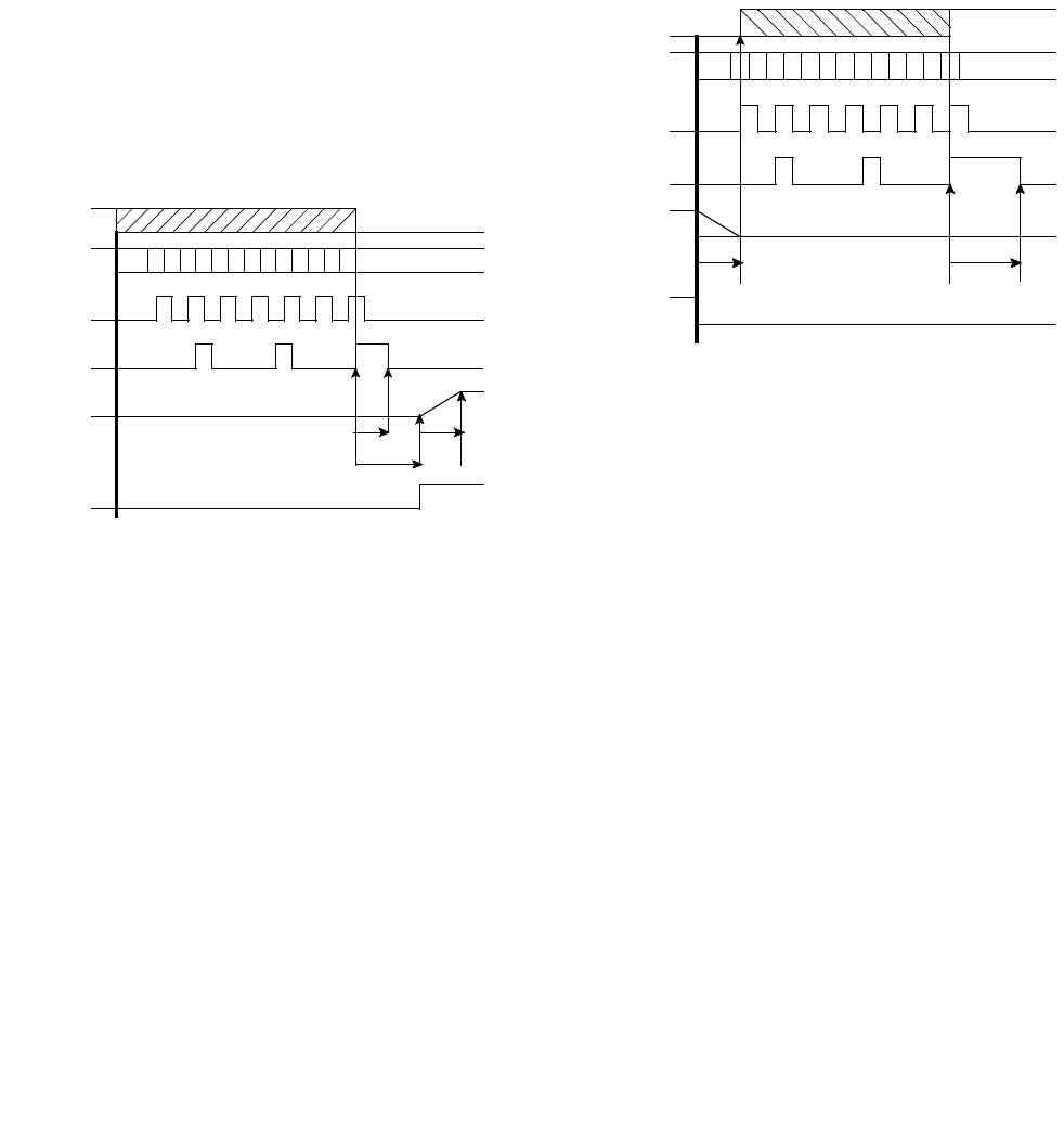
3.3 RECEIVE TO TRANSMIT SEQUENCE
1. Synthesizer is loaded (24-bit D, B and A0). Refer
to Figure 3-6.
2. The state of the RX_EN line does not have to be
changed until the last bit is sent. However, receive
will cease as soon as it is changed.
3. The SYNTH ENABLE line should be held HIGH
for 2 to 3 milliseconds after the last word is sent.
This puts the frequency synthesizer in a SPEEDUP
MODE and slightly improves lock times.
4. After the last word is strobed in, 7 milliseconds
(worst case) should elapse before TX_EN is turned
ON. This allows the synthesizer to come within
1 kHz of the desired frequency.
Figure 3-6 RX TO TX TIMING DIAGRAM
"Ramp-Up" is the amount of time required for the
transmitter to reach full power once the TX EN has
been applied. The Ramp-Up circuitry (located on the
transceiver) minimizes adjacent channel interference
caused by spectral spreading (sinx/x) when the trans-
mitter is keyed. The Ramp-Up time is approximately
3 ms.
D0D24D0 D24 D0 D24
"D" WORD "B" WORD "A" WORD
DATA
CLOCK
t=0
SPEEDUP RAMP-UP
LOCK
RX_EN
SYNTH_EN
9V TX
TX_EN
3.4 TRANSMIT TO RECEIVE SEQUENCE
1. TX_EN is turned OFF. This signal is shaped. Refer
to Figure 3-7.
2. The synthesizer load process could begin slightly
before, but when the last bit is strobed in the synthe-
sizer it will become unlocked.
3. The RX_EN line should switch from low to high
AFTER the TX_EN is switched. The RX_EN not
only turns the RX circuits on but also Pin Shifts the
VCO.
Figure 3-7 TX TO RX TIMING DIAGRAM
4. For quickest lock times the SYNTH ENABLE line
on the last load word should be held high for 2 to 3
milliseconds. It MUST NOT be left high as the syn-
thesizer in the SPEEDUP mode has poor noise per-
formance and would degrade the receiver
performance.
Speedup is 2 to 3 ms
Lock is approximately 7 ms
Ramp is approximately 3 ms
Dekey is approximately 3 ms
"Ramp-Down" is the amount of time required for
the transmitter output power to be reduced before
switching off the transmitter and enabling the receive
with the RX_EN. The Ramp-Down circuitry (located
on the transceiver) minimizes adjacent channel inter-
ference caused by spectral spreading (sinx/x) when the
transmitter is un-keyed. The Ramp-Down time is
approximately 3 ms.
D0D24D0 D24 D0 D24
"D" WORD "B" WORD "A" WORD
DATA
CLOCK
t=0
RAMP- SPEEDUP
RX_EN
SYNTH_EN
9V TX
TX_EN DOWN
PROGRAMMING
3-7
June 1997
Part No. 001-3412-002
IMPORTANT
If the receiver is to be operated at 510-512 MHz (-810),
a spurious condition may occur to degrade the receiver
sensitivity 2 to 3 dB. If this degradation is unaccept-
able, the synthesizer can be reprogrammed to a com-
parison frequency (FCM) of 31.25 kHz (so that a
multiple of this would not be 52.95 MHz) and a modu-
lus (FMOD) of 5 with a reference divide (NR) of 560.
These parameters place the spurious at harmonics of
31.25 kHz (instead of 50 kHz) outside the passband of
the IF filters where the sensitivity is not degraded.
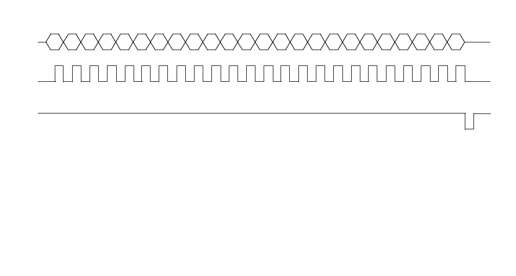
3.5 RADIO DIAGNOSTICS
The diagnostic features allow the user to program
a Digital-To-Analog Converter (DAC) to adjust RF
output power and modulation flatness without remov-
ing the radio from the enclosure. Bit "ao" can be set
to provide an analog voltage representative of the for-
ward and reverse RF power at the radio interface con-
nector J201, pin 14.
This feature can be used to monitor the condition
of the transceiver and antenna/feedline. Figure 3-8 is
a diagram of the Diagnostic Serial Data Stream with
definitions of the bits. It is 19-bits long, the front
(MSBs) can be padded with "Don’t Cares" (XXs) to
get to 24 bits.
Clock (max.) 1 MHz
Diag Enable (min) 250 ns (min)
XX Don’t Care
DAC Bits:
A1 - A0 = DAC Output Select
00=Power Set (Data=0xFF for now,
RNG=1)
01=Mod Adj (Data=0xFF for now,
RNG=1)
11=DAC Control Select (Data=0xFF for DAC Con-
trol)
RNG = Range Select (max. output) (Ref = 5.5V÷2)
0 = 1 x Ref
1 = 2 x Ref
D7 - D0 = D/A Data
0x00 = 0.0V
0xFF = 1 x Ref (RNG=0)
0xFF = approx. 2 x Ref (RNG=1)
Shift Register Bits:
a0 = Diagnostic Select to J201, pin 14 (Analog Voltage)
0 = Forward Power
1 = Reverse Power
Figure 3-8 DIAGNOSTIC SERIAL DATA STREAM
XXXX
XX XXXX A1 A0 Rng D7 D6 D5 D4 D3 D2 D1 D0 XXXX
XX XXXX XXXX ao
LSB (00)
MSB (23)
Data
Clock
Diag En

PROGRAMMING
3-8
June 1997
Part No. 001-3412-002
This page intentionally left blank.

4-1
June 1997
Part No. 001-3412-002
SECTION 4 CIRCUIT DESCRIPTION
4.1 GENERAL
4.1.1 INTRODUCTION
The main subassemblies of this transceiver are
the RF board, VCO board, TCXO and Loader board.
A block diagram of the transceiver is located in Figure
4-1. The 3412 is also available in transmit only and
receive only models.
The VCO board is enclosed by a metal shield and
soldered directly to the RF board. The VCO is not
serviceable.
The 3412 has a reference oscillator stability of
±1.5 PPM. The 17.5 MHz TCXO (Temperature Com-
pensated Crystal Oscillator) is soldered directly to the
RF board. The TCXO is not serviceable.
4.1.2 SYNTHESIZER
The VCO (voltage-controlled oscillator) output
signal is the receiver first injection frequency in the
Receive mode and the transmit frequency in the
Transmit mode. The first injection frequency is
52.95 MHz above the receive frequency. The fre-
quency of this oscillator is controlled by a DC voltage
produced by the phase detector in synthesizer chip
U811.
Channels are selected by programming counters
in U811 to divide by a certain number. This program-
ming is performed over a serial bus formed by the
Synth Clock, Synth Enable, and Data pins of J201.
This programming is performed by the Loader board
or user supplied hardware/software (see Section 3).
The frequency stability of the synthesizer in both
the receive and transmit modes is established by the
stability of the reference oscillator described in the
preceding section. These oscillators are stable over a
temperature range of -30° to +60° C (-22° to +140° F).
4.1.3 RECEIVER
The receiver is a double-conversion type with
intermediate frequencies of 52.95 MHz / 450 kHz.
Two helical bandpass filters reject the image, half IF,
injection, and other unwanted frequencies. A four-
pole crystal filter and an 8-pole ceramic filter enhance
receiver selectivity
4.1.4 TRANSMITTER
The transmitter produces a nominal RF power
output of 5W at 13.6V DC, adjustable down to 1W.
Frequency modulation of the transmit signal occurs in
the synthesizer. Transmit audio processing circuitry is
contained in the Loader board or customer-supplied
equipment.
4.1.5 LOADER BOARD
The Loader board, Part No. 023-3240-330, is a
plug-in circuit board used to load the synthesizer with
a desired frequency and filters data/audio to and from
the user interface connector. See Section 1.2.2.
4.2 SYNTHESIZER
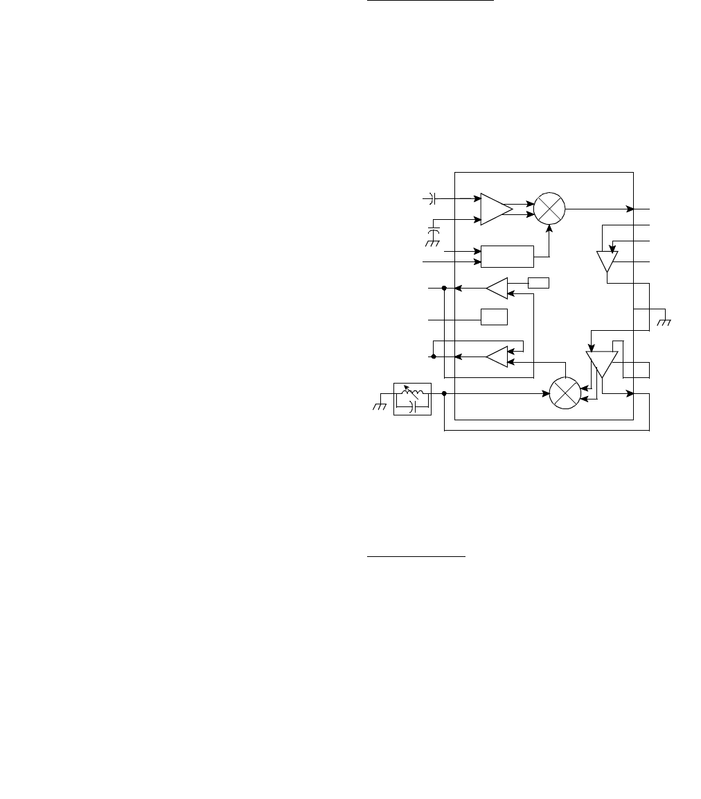
A block diagram of the transceiver is shown in
Figure 4-1 and a block diagram of Synthesizer IC
U811 is shown in Figure 4-2. As stated previously,
the synthesizer output signal is produced by a VCO
(voltage controlled oscillator). The VCO frequency is
controlled by a DC voltage produced by the phase
detector in U811. The phase detector senses the phase
and frequency of the two input signals and causes the
VCO control voltage to increase or decrease if they
are not the same. The VCO is then "locked" on fre-
quency.
Programming of the synthesizer provides the data
necessary for the internal prescaler and counters. One
input signal is the reference frequency. This frequency
is produced by the 17.5 MHz reference oscillator
(TCXO). The other input signal is the VCO
frequency.
CIRCUIT DESCRIPTION
4-2
June 1997
Part No. 001-3412-002
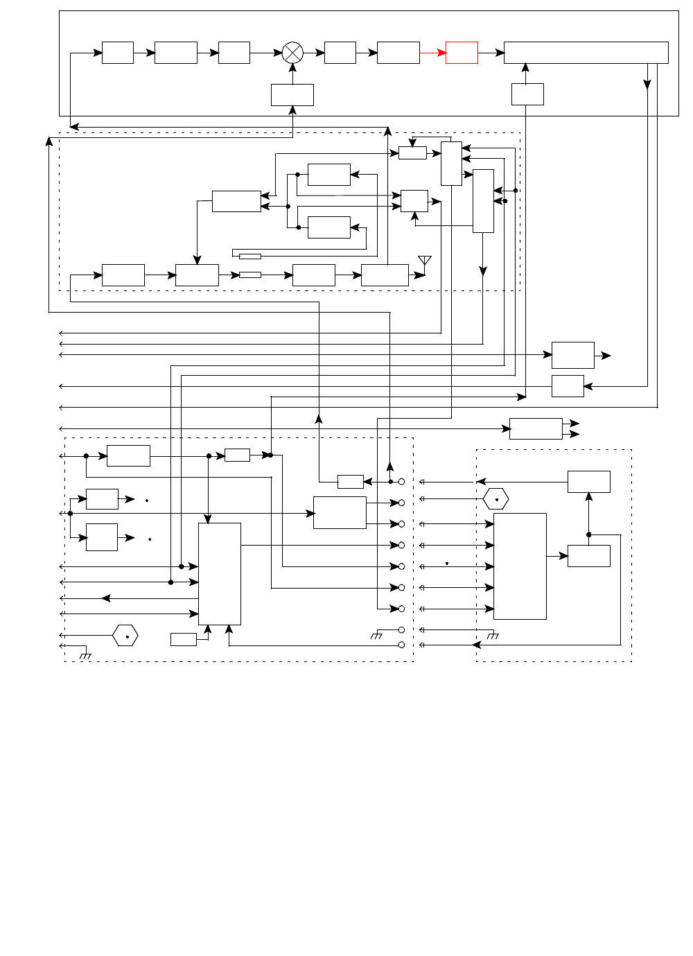
Figure 4-1 TRANSCEIVER BLOCK DIAGRAM
Z201
RF AMP
Z202
MIXER
CRYSTAL FILTER
PREDRIVER
ANTENNA
SWITCH
RX AUDIO
VCO
AMPLIFIER
T/R PS
SYNTHESIZER
VCO BUFFER/
RSSI
LOW-PASS
FILTER
RF OUT
RF BPF RF BPF U221
Z221/Z222
52.95 MHz IF / 450 kHz FILTER
Q401
2nd LO TRIPLER/AMP
1st LO AMP
CLV
Q853
Q851/Q852
AMPLIFIER
RSSI
RX OUT
TX IN
Y801
TCXO
MOD INPUT
MOD ADJUST
SYNTH OUT
RF IN
U811
BUFFER
U241
Q301
IF AMP
Q850
U521
TRANSMITTER
RECEIVER
+13.3V
+4.6V
U581B
U581A
PWR SET
DIAG
DIAG EN
MOD ADJ
DIAG
DIAG EN
TX EN +9V TX
RX EN
+13.3V
SWITCHED
CLOCK
DATA
ENABLE
LOCK
Q122
Q121
Q801
TEST
-2.0V
Q171
Q841, Q842
Q901, Q902
Q501
Q701
Q123
+5V DC
SHUTDOWN
Q511
Q531/U111C
CR561/562
V FWD
V REV U913C
U913A
U912
U261
Q131/U131
U141 +9.6V
+5.5V
Q231Q211Q201/Q202
Q101/Q102
U111A/B/D
Q124
U911
RSSI
RX OUT
TX EN
CLOCK
DATA
Q172
Q173 +9.6V
RECEIVE
CIRCUIT DESCRIPTION
4-3
June 1997
Part No. 001-3412-002
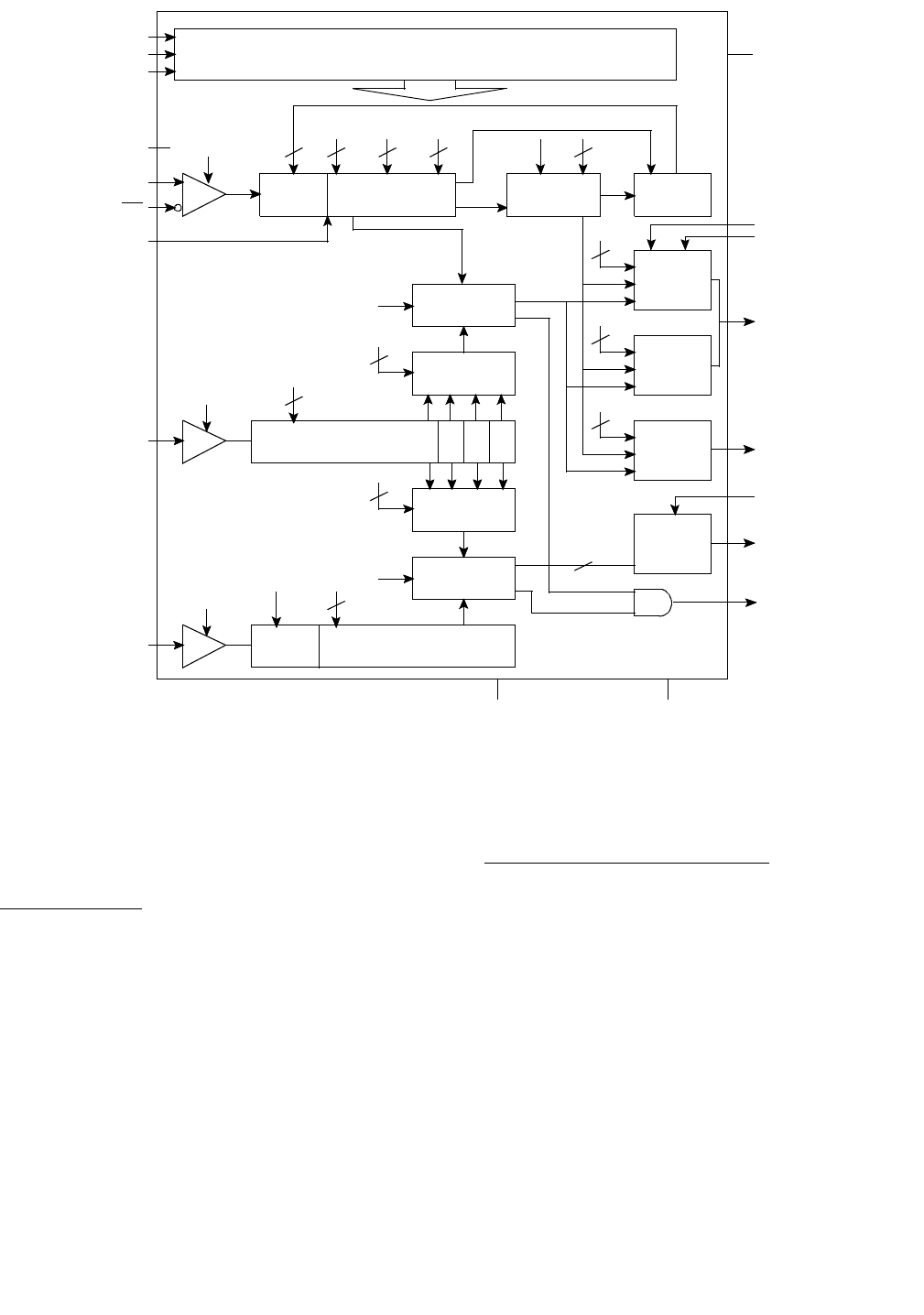
Figure 4-2 U801 SYNTHESIZER BLOCK DIAGRAM
CLOCK
DATA
STROBE
Vss
RF
IN
RF
IN
64/65/72
PRESCALER MAIN DIVIDERS
EM FB 2 2 12 8
PR NM1 NM3
NM2
FRACTIONAL
ACCUMULATOR
PRESCALER
MODULUS
CONTROL
3
FMOD NF
FB
SERIAL INPUT + PROGRAM LATCHES VDD
TEST
IN
REF
EM+EA
REFERENCE DIVIDER +2 +2 +2
MAIN
MAIN
PHASE
DETECTOR
REFERENCE
SELECT
2
SM
EM
REFERENCE
SELECT
2
SA
SECONDARY
PHASE
DETECTOR
EA AUXILIARY
IN
EA
AUX
12
NR
12
NAPA
AUXILIARY DIVIDER
PRESCALER
1/4
NORMAL
OUTPUT
CHARGE
PUMP
OUTPUT
CHARGE
PUMP
SPEED-UP
OUTPUT
CHARGE
PUMP
INTEGRAL
OUTPUT
CHARGE
PUMP
AUXILIARY
CN
8
CL
2
CK
4
2
VSSA
VDDA
LOCK
PHA
RA
PHI
PHP
RN
RF
Frequency Control and Modulation
The VCO frequency is controlled in part by DC
voltage across varactor diodes CR854, CR855, CR856
and CR851. As voltage across a reverse-biased varac-
tor diode increases, its capacitance decreases. There-
fore, VCO frequency increases as the control voltage
increases. CR854/CR855 and CR856/CR851 are par-
alleled varactors to divide the capacitance and
improve linearity. The varactors are biased at -2.0V
so the control line can operate closer to ground. The
control line is isolated from tank circuit RF by choke
L851/L854 and decoupling capacitor C854. The
amount of frequency change produced by CR854/
CR855/CR856/CR851 is controlled by series capaci-
tor C853.
4.2.1 VOLTAGE-CONTROLLED OSCILLATOR
Oscillator (Q850)
The VCO is formed by Q850, several capacitors
and varactor diodes, and ceramic resonator Z850. It
oscillates at the transmit frequency in transmit mode
and first injection frequency in the receive mode (380-
512 MHz in transmit and 432.950-564.950 MHz in
receive).
Biasing of Q850 is provided by R862, R867,
RC=867 and R868. An AC voltage divider formed by
C859, C861 and C862 initiates and maintains oscilla-
tion and also matches Q850 to the tank circuit.
Ceramic resonator Z850 is grounded at one end to pro-
vide shunt inductance to the tank circuit.

CIRCUIT DESCRIPTION
4-4
June 1997
Part No. 001-3412-002
The -2.0V applied to the VCO is derived from
the 17.5 MHz TCXO frequency that is amplified by
Q701, rectified by CR701 and filtered by C706, C707,
C708 and C709 on the RF board.
The VCO frequency is modulated using a similar
method. The transmit audio/data signal from J201,
pin 6 is applied across varactor diode CR852 which
varies the VCO frequency at an audio rate. Series
capacitors C856/C870 couple the VCO to CR852.
R854 provides a DC ground on the anodes of CR852/
CR853, and isolation is provided by R852 and C855.
C858 is an RF bypass. C853 provides isolation.
The DC voltage across CR853 provides compen-
sation to keep modulation relatively flat over the
entire bandwidth of the VCO. This compensation is
required because modulation tends to increase as the
VCO frequency gets higher (capacitance of CR854/
CR855/CR856/CR851 gets lower). CR853 also bal-
ances the modulation signals applied to the VCO and
TCXO. The DIAG on J201, pin 14 can also adjust the
modulation.
The DC voltage applied across CR853 comes
from the modulation adjust control R827 on the RF
board. R826 applies a DC biasing voltage to CR852;
C821 provides DC blocking. RF isolation is provided
by C858, R853 and R847.
4.2.2 VCO AND REFERENCE OSCILLATOR
MODULATION
Both the VCO and reference oscillator (TCXO)
are modulated in order to achieve the required fre-
quency response. If only the VCO were modulated,
the phase detector in U811 would sense the frequency
change and increase or decrease the VCO control volt-
age to counteract the change (especially at the lower
audio frequencies).
If only the reference oscillator frequency is mod-
ulated, the VCO frequency would not change fast
enough (especially at the higher audio frequencies).
Modulating both VCO and reference oscillators pro-
duces a flat audio response. Potentiometers R825,
R826 and R827 set the VCO modulation sensitivity so
that it is equal to the reference oscillator modulation
sensitivity.
4.2.3 CASCODE AMPLIFIERS/VCO (Q851/Q852)
Q851/Q852 form a cascode amplifier to provide
reverse isolation for the VCO. Q851 is configured as
a common emitter and Q852 as a common base. The
output signal is taken from the collector of Q851 and
coupled to the base of amplifier Q853 through cou-
pling capacitors C868, C871 and a PI-attenuator made
up of R859 and R875.
4.2.4 AMPLIFIER (Q853)
Amplifier Q853 provides final amplification of
the VCO signal. Bias for Q853 is provided by R871,
R872 and R874. L856/C874 provide a match to the
transmitter and first injection frequency. The T-pad
attenuator made up of R892, R893 and R894 provides
6 dB of isolation between the transmitter and first
injection frequency.
4.2.5 VOLTAGE FILTER (Q901)
Q901 on the RF board is a capacitance multiplier
to provide filtering of the 4.6V supply to the VCO.
R901 provides transistor bias and C901 provides the
capacitance that is multiplied. If a noise pulse or other
voltage change appears on the collector, the base volt-
age does not change significantly because of C901.
Therefore, base current does not change and transistor
current remains constant. CR901 decreases the charge
time of C901 when power is turned on. This shortens
the start-up time of the VCO. C902 and C903 are RF
decoupling capacitors.
4.2.6 VCO FREQUENCY SHIFT (Q841)
The VCO must be capable of producing frequen-
cies from 403-564.95 MHz to produce the required
receive injection and transmit frequencies. If this
large of a shift was achieved by varying the VCO con-
trol voltage, the VCO gain would be undesirably high.
Therefore, capacitance is switched in and out of the
tank circuit to provide a coarse shift in frequency.
This switching is controlled by the T/R pin shift
(RX_EN) on J201, pin 4, Q841/Q842 and pin diode
CR850. When a pin diode is forward biased, it pre-
sents a vary low impedance to RF; and when it is
reverse biased, it presents a very high impedance. The
capacitive leg is switched in when in transmit and out
when in receive.

CIRCUIT DESCRIPTION
4-5
June 1997
Part No. 001-3412-002
When J201, pin 4 is high in receive (+3-16V),
Q173 is turned on and the collector voltage goes low.
A low on the base of Q172 turns the transistor on and
the regulated +9.6V on the emitter is on the collector
for the receive circuitry. Q171 applies a low on the
base of Q841, the transistor is off and the collector is
high. With a high on the base of Q842 and a low on
the emitter, this reverse biases CR850 for a high
impedance.
The capacitive leg on the VCO board is formed
by C851, CR850, C852 and C876. When J201, pin 4
is low in transmit, Q842 is turned on and a high is on
the emitter, Q171 is turned off and the collector volt-
age goes high. A low on the base of Q173 turns the
transistor off and the regulated +9.6V is removed from
the receive circuitry. With a high on the base of Q841
the transistor is on and the collector is low. With a
low on the collector of Q842 and a high on the emit-
ter, this forward biases CR850 and provides an RF
ground through C851 and C852/C876 are effectively
connected to the tank circuit. This decreases the reso-
nant frequency of the tank circuit.
4.2.7 SYNTHESIZER IC (U811)
Introduction
Synthesizer chip U811 is shown in Figure 4-2.
This device contains the following circuits: R (refer-
ence), Fractional-N, NM1 and NM2; phase and lock
detectors, prescaler and counter programming
circuitry. The basic operation was described in
Section 4.2.1.
Channel Programming
Frequencies are selected by programming the R,
Fractional-N, NM1 and NM2 in U811 to divide by a
certain number. These counters are programmed by
Loader board or a user supplied programming circuit.
More information on programming is located in
Section 3.
As previously stated, the counter divide numbers
are chosen so that when the VCO is oscillating on the
correct frequency, the VCO-derived input to the phase
detector is the same frequency as the reference oscilla-
tor-derived frequency.
The VCO frequency is divided by the internal
prescaler and the main divider to produce the input to
the phase detector.
4.2.8 LOCK DETECT
When the synthesizer is locked on frequency, the
SYNTH LOCK output of U811, pin 18 (J201, pin 7) is
a high voltage. When the synthesizer is unlocked, the
output is a low voltage. Lock is defined as a phase
difference of less than 1 cycle of the TCXO.
4.3 RECEIVER CIRCUIT DESCRIPTION
4.3.1 HELICAL FILTER (Z201), RF AMPLIFIER
(Q201)
Capacitor C205 couples the receive signal from
the antenna switch to helical filter Z201. (The antenna
switch is described in Section 4.4.4.) Z201 is a band-
pass filter tuned to pass only a narrow band of fre-
quencies to the receiver. This attenuates the image
and other unwanted frequencies. The helicals are fac-
tory set and should not be tuned.
Impedance matching between the helical filter
and RF amplifier Q202 is provided by C206, C207
and L201. CR231 protects the base-emitter junction of
Q202 from excessive negative voltages that may occur
during high signal conditions. Q201 is a switched
constant current source which provides a base bias for
Q202. Q201 base bias is provided by R202/R203.
Current flows through R201 so that the voltage across
it equals the voltage across R202 (minus the base/
emitter drop of Q201). In the transmit mode the
receive +9.6V is removed and Q201 is off. This
removes the bias from Q202 and disables the RF
amplifier in transmit mode. This prevents noise and
RF from being amplified by Q202 and fed back on the
first injection line.
Additional filtering of the receive signal is pro-
vided by Z202. L202, C208 and C209 provide imped-
ance matching between Q202 and Z202. Resistor
R205 is used to lower the Q of L202 to make it less
frequency selective.
CIRCUIT DESCRIPTION
4-6
June 1997
Part No. 001-3412-002
4.3.2 MIXER (U211)
First mixer U211 mixes the receive frequency
with the first injection frequency to produce the
52.95 MHz first IF. Since high-side injection is used,
the injection frequency is 52.95 MHz above the
receive frequency. The RF signal is coupled to the
mixer through C215
4.3.3 FIRST LO AMPLIFIER (Q301)
The first injection frequency from the VCO is
coupled to the first local oscillator amplifier Q301
through C301. L301/C302 match Q301 to the VCO.
Bias for Q301 is provided by R301, R302 and R303,
R306 and C307. Impedance matching to the mixer is
provided by L302, R305 and C306 decouples RF sig-
nals.
4.3.4 BUFFER (Q211), CRYSTAL FILTER (Z221/
Z222), IF AMP (Q231)
The output of U221 is coupled to buffer Q211.
C213, R213 and Q211 match the 50 ohm output of
U221. Bias for Q211 is provided by R211 and R213.
The output of Q211 is matched to crystal filter Z221
via L211, C214 and R212.
Z221 and Z222 form a 2-section, 4-pole crystal
filter with a center frequency of 52.95 MHz and a
-3 dB passband of 8 kHz (12.5 kHz BW) or 15 kHz
(25 kHz BW). This filter establishes the receiver
selectivity by attenuating the adjacent channel and
other signals close to the receive frequency. C221,
C222, and L221 adjust the coupling of the filter.
L222, C223 and C233 provide impedance matching
between the filter and Q231.
IF amplifier Q231 amplifies the 52.95 MHz IF
signal to recover filter losses and improves receiver
sensitivity. Biasing for Q231 is provided by R231,
R232, R233, R234 and R235 and C232, C235 decou-
ple RF signals. The output of Q231 is coupled to the
detector by C234.
4.3.5 SECOND LO AMP/TRIPLER (Q401)
The input frequency to Q401 is 17.5 MHz from
TCXO Y801 coupled through C402. Bias for Q401 is
provided by R401, R402, R403 and R404. C403,
C404 decouple RF from the amplifier. L401, L402,
C405, C406 and C407 pass the third harmonic
(52.5 MHz) to the input of U241, pin 4. The output of
the amplifier is coupled to U241, pin 4 by C408, C409
and L403 form a 450 kHz notch.
4.3.6 SECOND MIXER/DETECTOR (U241)
Oscillator and Mixer
As shown in Figure 4-3, U241 contains the sec-
ond oscillator, second mixer, limiter, detector, and
squelch circuitry. The 52.95 MHz IF signal is mixed
with a 52.5 MHz signal produced by second LO
amplifier/tripler Q401 from TCXO Y801.
Figure 4-3 U241 BLOCK DIAGRAM
Second IF Filter
The output of the internal double-balanced mixer
is the difference between 52.95 MHz and 52.5 MHz
which is 450 kHz. This 450 kHz signal is fed out on
pin 20 and filtered by IF filter Z251. The filtered sig-
nal is fed back into U241 on pin 18 to an internal IF
amplifier. After amplification the signal is fed out on
pin 16 where it is filtered by Z252 and then fed back
into U241, pin 14 to the limiter.
1
2
4
MIXER
5
15
14
11
RSSI
52.95 MHz
C234
C267
20
OSCILLATOR
52.5 MHz
+
-
RSSI OUTPUT
9
VREG
6
VCC
7
8
+
-
10 QUAD
AUDIO OUTPUT
L253
12
13
3
NC
LIMITER IN
LIMITER
IF AMP OUT
IF DEC1
IF DEC2
IF AMP IN
MIXER OUT
LIMITER DEC1
LIMITER DEC2
LIMITER OUT
IF AMP
16
17
18
19
RSSI FB
AUDIO FB

CIRCUIT DESCRIPTION
4-7
June 1997
Part No. 001-3412-002
Limiter-Amplifier
The output of Z252 is applied to a limiter-ampli-
fier circuit in U241. This circuit amplifies the 450
kHz signal and any noise present; then limits this sig-
nal to a specific value. When the 450 kHz signal level
is high, noise pulses tend to get clipped off by the lim-
iter; however, when the 450 kHz signal level is low,
the noise passes through the limiter. C275/C276
decouple the 450 kHz signal.
Quadrature Detector
From the limiter stage the signal is fed to the
quadrature detector. An external phase-shift network
connected to pin 8 shifts the phase of one of the detec-
tor inputs 90° at 450 kHz (all other inputs are
unshifted in phase). When modulation occurs, the fre-
quency of the IF signal changes at an audio rate as
does the phase of the shifted input. The detector,
which has no output with a 90° phase shift, converts
this phase shift into an audio signal. L253 is tuned to
provide maximum undistorted output from the detec-
tor. R255 is used to lower the Q of L253. From the
detector the audio and data signal is fed out on pin 8.
Audio/Data Amplifier
The audio/data output of U241, pin 8 is fed to the
audio amplifier U261. U261 amplifies and inverts the
detected audio/data signal and shifts the DC bias level
to +2.5V DC at the output on pin 13. The gain is set at
approximately 2.5 by R262/R263. R264/R265 pro-
vide a 1.3V DC reference bias voltage for U241. The
audio output of U261 is applied to J201, pin 13.
Receive Signal Strength Indicator (RSSI)
U241, pin 5 is an output for the RSSI circuit
which provides a voltage proportional to the strength
of the 450 kHz IF signal. The RSSI voltage is applied
to J201, pin 12.
4.4 TRANSMITTER CIRCUIT DESCRIPTION
4.4.1 BUFFER (Q501)
The VCO RF output signal is applied to R892,
R893 and R894 that form a resistive splitter for the
receive first local oscillator and the transmitter. The
VCO signal is then applied to a 50 ohm pad formed by
R501, R502, and R503. This pad provides attenuation
and isolation. Q501 provides amplification and addi-
tional isolation between the VCO and transmitter.
Biasing for this stage is provided by R504 and R505,
and decoupling of RF signals is provided by C503 .
Impedance matching to the predriver is provided by
L511 and C512.
4.4.2 PRE-DRIVER (Q511)
Pre-driver Q511 is biased Class A by R511,
R512, R513 and R515. L513, C517 and C518 match
Q511 to U521. R514 provides a resistive feedback
path to stabilize Q511 and C515 provides DC block-
ing. C516 bypasses RF from the DC line, and R513
provides supply voltage isolation and ties the +9V
transmit supply to the circuit.
4.4.3 FINAL (U521), COMPARATOR (U111C)
RF module U521 has an RF output of 1 to 5W
and operates on an input voltage from 10-16V.
Power control is provided by U581, U111, Q531
and a stripline directional coupler. The power is
adjusted by Power Set Control of U911 by R535 that
provides a reference voltage to U111C. U111C drives
Q531 and PA module U521.
One end of the stripline directional coupler is
connected to a forward RF peak detector formed by
R591, CR591, C591 and U581A. The other end of the
stripline directional coupler is connected to a reverse
RF peak detector formed by R593, CR592, C593 and
U581B.
If the power output of U521 decreases due to
temperature variations, etc., the forward peak detector
voltage drops. This detector voltage drop is buffered
by U581A and applied to inverting amplifier U111C
which increases the forward bias on Q531. The
increase on Q531 increases the power output level of
U521. If the power output of U521 increases, the for-
ward peak detector voltage increases and U111C
decreases the forward bias on Q531. The decrease on
Q531 decreases the output power of U521.
The output of CR591 and CR592 are fed to
U581A/B respectively. If the output of either buffer
increases, the increase is applied to the inverting input
of U111C. The output of U111C then decreases and

CIRCUIT DESCRIPTION
4-8
June 1997
Part No. 001-3412-002
Q531 decreases the input voltage to U521 to lower the
power. The control voltage is isolated from RF by fer-
rite bead EP532 and C531 decouples RF.
The forward/reverse power voltages from
U581A/B are also applied to U913 for Diagnostic out-
puts on J201, pin 14.
The low-pass filter consists of C552, L551,
C553, L552, C554, L553, C555, L554 and C556. The
filter attenuates spurious frequencies occurring above
the transmit frequency band. The transmit signal is
then fed through the antenna switch to antenna jack
J501.
4.4.4 ANTENNA SWITCH (CR561, CR562)
The antenna switching circuit switches the
antenna to the receiver in the receive mode and the
transmitter in the transmit mode. In the transmit
mode, +9V is applied to L555 and current flows
through diode CR561, L561, diode CR562, and R561.
When a diode is forward biased, it presents a low
impedance to the RF signal; conversely, when it is
reverse biased (or not conducting), it presents a high
impedance (small capacitance). Therefore, when
CR561 is forward biased, the transmit signal has a
low-impedance path to the antenna through coupling
capacitor C562.
C583, L561, and C564 form a discrete quarter-
wave line. When CR561 is forward biased, this quar-
ter-wave line is effectively AC grounded on one end
by C564. When a quarter-wave line is grounded on
one end, the other end presents a high impedance to
the quarter-wave frequency. This blocks the transmit
signal from the receiver. C561/C562 matches the
antenna to 50 ohms in transmit and receive.
4.4.5 TRANSMIT KEY-UP CONTROL
Q121, Q122 and Q123 act as switches which turn
on with the RX_EN line. When the line goes low
Q121 is turned off, which turns Q122 on, turning
Q123 on. This applies 13.6V to U111 before the
TX_EN line goes high.
U111A/B provide the key-up and key-down con-
ditioning circuit. C116 and R117 provide a ramp-up
and ramp-down of the 9V transmit supply during key-
up and key-down which reduces load pull of the VCO
during key-up. The conditioning provides a stable
5.5V output by balancing the 5.5V reference with the
5.5V regulated supply.
The output on U111B, pin 7 is applied to the non-
inverting input of comparator U111D, pin 12. The
output of U111D, pin 14 is applied to the base of cur-
rent source Q124. The output of Q124 is on the emit-
ter and is applied back to the inverting input of com-
parator U111D, pin 13. A decrease or increase at
U111D, pin 13 causes a correction by U111D to stabi-
lize the 9V transmit output. R125/R126 establishes
the reference voltage on U111D, pin 13. C123 pro-
vides RF bypass, C124 provides RF decoupling and
C125 stabilizes the output. The 9V transmit voltage is
then distributed to the circuits.
4.5 VOLTAGE REGULATORS
4.5.1 +9.6 AND +5.5V REGULATED
The +5-16V applied on J201, pin 5 is applied to
the base of Q131 turning the transistor on. This
causes the collector to go low and applies a low to the
control line of U131, pin 2 and R132 provides supply
voltage isolation. The 13.3V from J201, pin 2 is on
U131, pin 6 to produce a +5.5V reference output on
U131, pin 4. C132 stabilizes the voltage and C131/
C133 provide RF decoupling. C134 provides RF
bypass and C136 provides RF decoupling. C135
helps to stabilize the voltage when the +5.5V supply
first turned on.
The low from the collector of Q131 is also
applied to the control line of U141, pin 2. The 13.3V
from J201, pin 2 is on U141, pin 6 to produce a +9.6V
output on U141, pin 4. C144 provides RF bypass and
C146 provides RF decoupling. C145 helps to stabilize
the voltage when the +9.6V supply first turned on.

5-1
June 1997
Part No. 001-3412-002
SECTION 5 SERVICING
5.1 GENERAL
5.1.1 PERIODIC CHECKS
This transceiver should be put on a regular main-
tenance schedule and an accurate performance record
maintained. Important checks are receiver sensitivity
and transmitter frequency, modulation, and power out-
put. A procedure for these and other tests is located in
Section 6. It is recommended that transceiver perfor-
mance be checked annually even though periodic
checks are not required by the FCC. During the first
year, make an additional check or two to ensure no
TCXO frequency drifting has occurred.
5.1.2 SURFACE-MOUNTED COMPONENTS
A large number of the components used on the
transceiver board are the surface-mounted type. Since
these components are relatively small in size and are
soldered directly to the PC board, care must be used
when they are replaced to prevent damage to the com-
ponent or PC board. Surface-mounted components
should not be reused because they may be damaged by
the unsoldering process.
5.1.3 SCHEMATIC DIAGRAMS AND COMPO-
NENT LAYOUTS
Schematic diagrams and component layouts of
the PC boards used in this transceiver are located in
Section 8. A component locator guide is also pro-
vided to aid in component location.
5.1.4 REPLACEMENT PARTS LIST
A replacement parts list with all the parts used in
this transceiver is located in Section 7. Parts are listed
alphanumerically according to designator. For infor-
mation on ordering parts, refer to Section 1.8.
5.1.5 TCXO MODULE NOT SERVICEABLE
The ±1.5 PPM TCXO module is not field ser-
viceable. Part changes require a factory recalibration
to ensure that the oscillator stays within its ±1.5 PPM
tolerance.
5.2 SYNTHESIZER SERVICING
5.2.1 INTRODUCTION
When there is a synthesizer malfunction, the
VCO is not locked on frequency. When an unlocked
VCO is detected by the lock detector circuit, U801,
pin 18 goes low (0V).
NOTE: The user-supplied circuitry must disable the
transmitter and receiver when an out-of-lock condi-
tion is indicated.
When the VCO is unlocked, the fR and fV inputs
to the phase detector are not in phase (see Section
4.1.2). The phase detector in U801 then causes the
VCO control voltage to go to the high or low end of
its operating range. This in turn causes the VCO to
oscillate at the high or low end of its frequency range.
As shown in Figure 4-1, a loop is formed by
VCO Q850, amplifier Q851/Q852, and the RF IN of
U801. Therefore, if any of these components begin to
malfunction, improper signals appear throughout the
loop. However, correct operation of the counters can
still be verified by measuring the input and output fre-
quencies to check the divide number.
Proceed as follows to check the synthesizer I/O
signals to determine if it is operating properly.
5.2.2 REFERENCE OSCILLATOR
Check the signal at U811, pin 8. It should be
17.5 MHz at a level of approximately 1V P-P. If the
TCXO module is defective, it is not serviceable and
must be replaced with a new module as described in
Section 5.1.5.
5.2.3 VCO
Output Level
The output level of Q853 can be measured with
an RF voltmeter or some other type of high impedance
meter. The minimum level after a power splitter at
R893 should be -10 dBm.
SERVICING
5-2
June 1997
Part No. 001-3412-002
Control Voltage
Check the DC voltage at TP831 with a channel
near the center of the band. If the VCO is locked on
frequency, this should be a steady DC voltage near
3V. If it is not locked on frequency, it should be near
the lower or upper end of its range (0V or 5.5V).
Output Frequency
Check the VCO frequency at R893. If the VCO
is locked on frequency, it should be stable on the
transmit channel frequency. If the VCO is not locked
on frequency, the VCO control voltage is probably
near 0V or 5.5V.
5.2.4 SYNTHESIZER (U801)
Lock Detector
When the VCO is locked on frequency, the lock
detect output on J201, pin 7 should be high.
5.3 RECEIVER SERVICING
To isolate a receiver problem to a specific sec-
tion, refer to the troubleshooting flowchart in Figure
5-1. Tests referenced in the flowchart are described in
the following information.
NOTE: Supply voltages are provided by the user.
5.3.1 SUPPLY VOLTAGES AND CURRENT
Measure the supply voltages on the following
pins at interface connector J201:
Pin 2 - 13.3V DC nominal
Pin 3 - 0.0V DC while in Receive
Pin 4 - 3-16V DC in Receive Mode
Pin 5 - 3-16V DC
Pin 6 - 2.5V DC ±1%
Place a DC ammeter in the supply line to the
transceiver and the following maximum currents
should be measured:
Pin 4 - 150 µA
5.3.2 MIXER/DETECTOR (U241)
Data Output
Using a .01 µF coupling capacitor, inject a
52.95 MHz, 1 mV signal, modulated with 1 kHz at
± 3 kHz deviation at U241, pin 1. The signal output at
U241, pin 8 should be approximately 150 mV P-P.
NOTE: This signal consists of the 1 kHz modulation
and harmonics of 450 kHz.
RSSI Output
The RSSI output on J201, pin 12 should be
<900 mV DC with no signal applied, and >2.3V DC
with a 1 mV input signal.
Figure 5-1 RECEIVER SERVICING
START
MEASURE CURRENT
OK
?
OK
?
NO
YES
YES
NO
REFER TO SECTION 5.3.2
CHECK FUSES AND
WIRE HARNESS CONNECTIONS
REFER TO SECTION 5.3
AND VOLTAGES
CHECK DATA
OUTPUT
REFER TO SECTION 5.3.2
CHECK
CHECK AUDIO
OK
?
YES
NO
OK
?
YES
NO
CHECK MIXER/
DETECT CIRCUIT
U241
CIRCUIT REFER TO SECTION 5.3.4
REFER TO SECTION 5.3.3
REPLACE DEFECTIVE
COMPONENT
REFER TO SECTION 5.3.6
CHECK BUFFERS
CRYSTAL FILTERS
REPAIR DEFECTIVE
STAGE
CHECK RF AMP
FIRST MIXER REFER TO SECTION 5.3.3

SERVICING
5-3
June 1997
Part No. 001-3412-002
5.3.3 SECOND LO (Q401)
Verify the Second LO signal is present at U241,
pin 4. The Second LO should be at 52.50 MHz and
not less than 500 mV P-P.
5.3.4 AUDIO BUFFER AMP (U261)
The Data output on J201, pin 13 should be 280-
700 mV P-P, with the preceding injection signal. If
these levels are not correct, verify proper adjustment
of L253 (see Section 6.3). The gain of U261 is 2.5 for
25 kHz radios and 5 for 12.5 kHz radios.
5.3.5 IF AMP (U231)
The IF Amp input signal is 52.95 MHz. This
amp provides approximately 15 dB of gain to U241.
5.3.6 BUFFER AMP (Q211), CRYSTAL FILTERS
Q211 buffers the 52.95 MHz IF signal and pro-
vides matching to the crystal filters Z221/Z222.
5.3.7 MIXER (U211)
The mixer converts the RF signal (380-512 MHz)
to 52.95 MHz. The Local Oscillator is provided by
the VCO and Q301. The level of the LO should be
approximately +3 dBm.
5.3.8 LNA (Q202), HELICAL FILTERS
The LNA provides approximately 15 dB of gain
at 380-512 MHz. The helical filters Z201/Z202 have
approximately 2.5 dB of loss each. Q201 provides
active bias to Q201.
5.3.9 ANTENNA SWITCH
CR561, CR562, L561, C561 and C563 form a Pi
network antenna switch. CR561 and CR562 are
reversed biased in Receive Mode.
5.4 TRANSMITTER SERVICING
5.4.1 SUPPLY VOLTAGES AND CURRENT
Measure the supply voltages on the following
pins of interface connector J201:
Pin 2 - 13.3V DC nominal
Pin 3 - 3-16V DC
Pin 4 - 0.0V DC (while transmitting)
Pin 5 - 3-16V DC
Pin 6 - 2.5V DC ±1%/1.5V P-P max
Place a DC ammeter in the supply line to the
transceiver and the following maximum currents
should be measured:
Pin 2 - 2.5A maximum
Pin 3 - 150 µA
Pin 5 - 150 µA
5.4.2 VCO (A801)
1. Check VCO A801 for power output.
(Power output should be at least -10 dBm.)
2. Check 9V Transmit (Q141, emitter).
3. If 9V is not present check Q124, U111, Q121,
Q122, Q123, Q101 and Q102 (see Section 4.4.5).
4. Check voltages on Buffer Q501.
Input = 1.5V DC
Output = 3.5V DC
Power output should be at least 2 mW (+3 dBm) at
C504 (50 ohm point).
5.4.3 PRE-DRIVER (Q511)
1. Check voltages on Q511.
Collector = 8.6V DC
Base = 2.2V DC
Emitter = 1.6V DC w/o RF (2.2V DC with RF)
Power output should be at least 100 mW (+13 dBm)
at the junction of C517/L518 (50 ohm point).
SERVICING
5-4
June 1997
Part No. 001-3412-002
5.4.4 FINAL AMPLIFIER (U521)
1. Check the voltages on U521.
Pin 2 = 5.5V DC (varies with power setting)
Pin 3 = 5.0V DC
Pin 4 = 12.7V DC
Power output at C551 should be 7.5-8.0W (+38.7 to
+39 dBm).
5.4.5 ANTENNA SWITCH (CR561/CR562)
1. Check the antenna switch voltages.
CR561 = 8.6V DC
CR562 = 8.0V DC
The loss through the Antenna Switch should be 1.9
to 2.1 dB.
5.4.6 MODULATION INPUT (J201, PIN 6)
1. Check for audio/data signals at J201, pin 6, Y801,
pin 1 and A801, pin 3.
5.4.7 TCXO (Y801)
1. Check Y801, pin 1 for 2.5V DC ±1%.
2. Adjust Y801 to set the transmitter to the frequency
of operation.
3. If the frequency cannot be set to the frequency of
operation, replace the TCXO.
Figure 5-2 TRANSMITTER SERVICING
START
MEASURE
CURRENT AND
OK
?
NO
YES
MEASURE RF
WATTS
?
CHECK DEVIATION
TRANSMITTER
OK
OK
?
OK
?
NO
NO
NO
YES
YES
YES
WIRE HARNESS CONNECTIONS
CHECK FUSES AND
CHECK AUDIO
CHECK TCXO
ADJUST OR
CHANGE TCXO
OFF FREQ
5
VOLTAGES
OUTPUT POWER
(SECTION 5.4.6)
CIRCUITS
CHECK FREQUENCY
(SECTION 5.4.7)
Y801
OK
?
NO
YES
CHECK Q501
REFER TO
CHECK PRE-DRIVER
OK
?
NO
YES
CHECK A801
REFER TO
SECTION 5.4.2
CHECK DRIVER
SECTION 5.4.3
CHECK Q511
OK
?
NO
YES
REFER TO CHECK
POWER MODULE
SECTION 5.4.4
CHECK U521
OK
?
NO
REFER TO CHECK
ANTENNA SWITCH
SECTION 5.4.5
CHECK
CR561/562
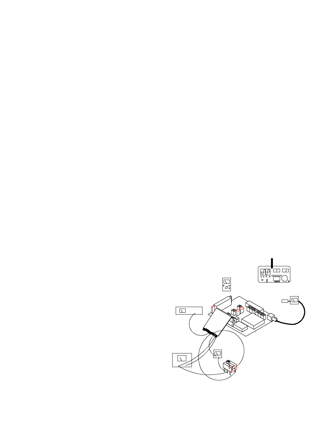
6-1
June 1997
Part No. 001-3412-002
SECTION 6 ALIGNMENT PROCEDURE AND PERFORMANCE TESTS
6.1 GENERAL
Receiver or transmitter alignment may be neces-
sary if repairs are made that could affect tuning.
Alignment points diagrams are located in Figure 6-4
or component layouts are located in Section 8.
Fabricate test cables by referring to Figure 2-1.
This cable should include power and ground, a trans-
mit keying switch that shorts the keying line to
ground, data input and data output. The test setup
must apply the various supply voltages and load the
synthesizer with channel information.
6.2 TEST EQUIPMENT
lModulation Analyzer, HP8901 or equivalent
lRF Signal Generator, HP8656 or equivalent
lPower Meter
lOscilloscope
lDigital Multimeter
lPower Supply, HP8264A or equivalent
lAudio Analyzer, HP8903A or equivalent
lLoader Board (PN 023-3240-330) or equivalent
6.3 DL3412 TRANSCEIVER ONLY
6.3.1 VCO CONTROL VOLTAGE
1. Connect the test setup shown in Figure 6-1. Set the
power supply for +13.3V DC. See Figure 2-1 for
interface cable.
2. Load the synthesizer with the channel frequency
(see Section 3.2).
3. Connect a DC voltmeter at the junction of R833/
C836 (VCO pin 16) to measure the VCO control
line voltage for a meter reading of ≥ 0.50 and
≤ 4.90V DC (see Figure 6-4).
NOTE: These voltages will be approximately 0.50V
DC higher with the VCO cover off.
4. Adjust R535 fully counterclockwise and key the
transmitter.
5. Connect a DC voltmeter at the junction of R833/
C836 (VCO pin 16) to measure the VCO control
line voltage for a meter reading of ≥ 0.75 and
≤ 5.00V DC (see Figure 6-4).
NOTE: These voltages will be approximately 0.50V
DC higher with the VCO cover off.
6. Unkey the transmitter.
6.3.2 TRANSMITTER AND FREQUENCY ALIGN-
MENT (OEM Not Using Diagnostics)
1. Connect the test setup shown in Figure 6-1. A DC
ammeter capable of measuring up to 3A should be
installed in the supply line. Set the input voltage for
+13.3V DC.
2. Load the synthesizer with the channel frequency.
(Do not transmit for extended periods.)
3. Adjust R535 clockwise for 5.0W +0.5/-0.2W.
Power output should be between 4.0-6.0W with cur-
rent less than 2.5A (subtract 30 mA if Loader Board
is used).
Figure 6-1 TRANSMITTER TEST SETUP
POWER SUPPLY
+13.3V DC
TX
RX
VOLTMETER
DC
+
-
WATTMETER5W, 50 OHM
DUMMY LOAD
COMMUNICATIONS
SERVICE MONITOR
0-1.5A
DC AMMETER
+-
ANALYZER
MODULATION

ALIGNMENT PROCEDURE AND PERFORMANCE TESTS
6-2
June 1997
Part No. 001-3412-002
6.3.3 MODULATION ALIGNMENT
1. Connect a DC voltmeter to the junction of R822/
R823 and adjust R823 for 2.10V DC ±0.05V DC
(see Figure 6-4).
2. Inject a 100 Hz square-wave tone at approximately
0.35V P-P, biased at +2.5V DC on J201, pin 6.
3. Transmit into the modulation analyzer and observe
modulation output on the oscilloscope. Set the
modulation analyzer high pass filtering off and no
less than a 15 kHz low pass filter.
4. Adjust R827 for a flat square-wave on the
oscilloscope. (The voltage at the wiper of R827
should be between 1-3V DC. If the voltage is less
than 1V DC, replace R825 with a larger value.)
5. Inject a 100 Hz sine-wave on J201, pin 6, biased at
+2.5V DC, the modulation analyzer should still
have the 15 kHz lowpass filter selected.
6. Adjust the audio analyzer output level to achieve a
transmit deviation of:
1.5 kHz for 12.5 kHz BW (-X10 Radios)
3.0 kHz for 25.0 kHz BW (-X30 Radios)
7. Set a 0 dB reference of FM peak deviation on the
Audio Analyzer.
8. Input a 1kHz sine-wave. The level should be within
±1.5 dB of the reference at 100 Hz.
0.2V RMS for 12.5 kHz BW (-X10 Radios)
0.4V RMS for 25.0 kHz BW (-X30 Radios)
9. Remove transmit modulation and unkey the
transmitter.
6.3.4 TRANSMITTER AND FREQUENCY ALIGN-
MENT (Johnson Loader Using Diagnostics)
NOTE: Subtract the current drawn by the test loader
or any interface units from all measurements.
NOTE: Refer to DL-3240 Universal Loader Board
Service Manual for software description and program-
ming information. The PRODUCTION TEST : TEST
SELECT menu is required for alignment.
1. Check that R571 is installed and R572 is removed
on Revision 2 or earlier boards (see Figure 6-4).
2. Make sure input supply voltage equals +13.3V.
3. Arrow to the "mid" channel.
4. Press F5 to key the transmitter (see Figure 6-2).
5. Adjust R535 fully clockwise for maximum power
output.
6. Adjust the DAC value using PgUp/PgDn to set the
power out to 5.0W ±0.3W. Re-check supply volt-
age for +13.3V. Adjust voltage and power if neces-
sary (see Figure 6-2).
7. Repeat Step 6 at the "low" and "high" channels.
8. Power output should be 4.7-5.3W (50% Duty
Cycle) and current less than 2.5A for 380-512 MHz
Transmitters.
9. Arrow to the "mid" channel. Adjust the frequency
displayed on the Frequency Counter to read accord-
ing to the frequency shown on the monitor by
adjusting the TCXO (Y801).
10.Observe the Forward Power voltage on the monitor.
The voltage should be greater than 3.0V DC.
11.Observe the Reverse Power voltage on the monitor.
The voltage should be less than 1.0V DC.
6.3.5 MODULATION ADJUSTMENT
1. Arrow down to Square Wave and arrow over to tog-
gle the 100 Hz square-wave tone on.
2. Transmit into the modulation analyzer and observe
modulation output on the oscilloscope. The modu-
lation analyzer should not have any high pass filter-
ing selected and no less than a 15 kHz low pass
filter.
3. Check to be sure the DAC values are at there initial
settings. Press F3 to initialize the Power Adjust,
Mod Adjust, and Front-End Adjust if they are not
initialized (see Figure 6-2).

ALIGNMENT PROCEDURE AND PERFORMANCE TESTS
6-3
June 1997
Part No. 001-3412-002
4. Arrow to the "mid" channel the DAC value should
be "125" (the voltage at the wiper of R827 should be
set to 1.5V DC). If the square wave is rolled off on
the edges, adjust R825 up in value to achieve as flat
a square wave as possible. If the square wave is
peaked on the edges, adjust R825 down in value to
achieve as flat a square wave as possible.
5. Adjust the DAC value using CTRL Page Up/Page
Down to fine tune the DAC value for the latest
square wave (see Figure 6-2).
6. If the radio/loader combination is to stay together as
one unit, press F10 to save the values to the loader
EEPROM.
7. Repeat the previous two steps at the Low and High
channels.
8. Arrow down to Square Wave and arrow over to shut
the square wave off.
9. Arrow up to Tx Audio Mode and arrow over to
Wide AC.
10.Input a 100 Hz sine wave. With the modulation
analyzer 15 kHz low pass filter selected. Adjust the
audio analyzer output level to achieve a transmit
deviation of:
fd= 1.5 kHz for 12.5 kHz radios
fd= 3.0 kHz for 25 kHz radios
11.Arrow to the Low channel, input a 100 Hz sine
wave and set a 0 dB reference on the MOdulation
Analyzer. Input a 1 kHz sine wave, the level should
be within ±0.5 dB of the reference at 100 Hz.
12.Arrow to the "mid" channel, input a 100 Hz sine
wave and set a 0 dB reference on the MOdulation
Analyzer. Input a 1 kHz sine wave, the level should
be within ±0.5 dB of the reference at 100 Hz.
13.Arrow to the High channel, input a 100 Hz sine
wave and set a 0 dB reference on the MOdulation
Analyzer. Input a 1 kHz sine wave, the level should
be within .05 dB of the reference at 100 Hz.
14.Unkey the transmitter by pressing F6.
Figure 6-2 PRODUCTION TEST:TEST SELECT
Radio
Freq Pair
Range
Rx Frequency
Tx Frequency
Rx Audio Mode
Tx Audio Mode
600 Ohm Input
Square Wave
Carrier Squelch
PgUp/Dn:
CTRL PgUp/Dn:
ALT PgUp/Dn:
= 3412
= MID
= 1
= 450.000000 MHz
= 450.000000 MHz
= Audio
= Audio
= OFF
= OFF
= ON
Power Adj
Mod Adj
Front End Adj
F2: Auto Front-End Adjust
F5: PTT On
F9: Toggle Sleep Mode
Frequency Pair (Left/Right Arrow to Select)
F3: Init Tune Settings
F6: PTT Off
F10: Save Power/Mod/Front-End Adj for Pair
F4: Start Heat Run
F7: Direct DAC Adj
Frequency Select (ESC to Exit)
RSSI Voltage
Forware Power
Reverse Power
Voltage
Current
Temperature
VSWR
Power Adj
MOd Adj
Front-End Adj
Diag-En Adj
Synth Lock
= 0.70 V
= 2.40 V
= 0.60 V
= 13.3 V
= 0.09 A
= 89 F
= 1.4:1
= 89
= 102
= 122
= 255
File Edit Utilities Program Code Prod Test <F1>-Help 08:43:30
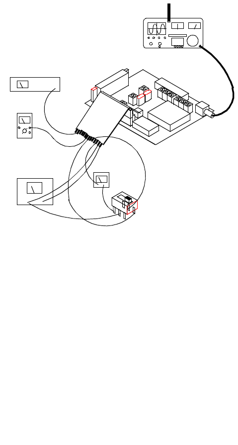
ALIGNMENT PROCEDURE AND PERFORMANCE TESTS
6-4
June 1997
Part No. 001-3412-002
6.3.6 RECEIVER ALIGNMENT
C A U T I O N
Do not key the transmitter with the generator con-
nected because severe generator damage may result.
1. Connect the test setup shown in Figure 6-3. Adjust
the power supply for +13.3V DC.
2. Measure the receive current drain. (Typically cur-
rent should be approximately 88 mA or 105 mA
with Loader Board.)
3. Preset tuning slugs of L211/L222 to the full clock-
wise position (slug in all the way).
4. Preset C221 to center position (slot in-line with axis
of part).
5. Readjust L222 counterclockwise 2 turns.
Figure 6-3 RECEIVER TEST SETUP
6.3.7 IF AND AUDIO ADJUSTMENTS
1. Load the synthesizer with the channel frequency.
2. Set the RF signal generator for this frequency with
a 1 kHz tone (modulated output shown below) at a
level of -47 dBm (1000 µV) and inject into J501.
1.5 kHz deviation 12.5 kHz BW (-X10 Radio)
3.0 kHz deviation 25.0 kHz BW (-X30 Radio)
NOTE: Maintain these deviation levels throughout
the test when measuring AC levels, SINAD and %
distortion.
3. Adjust L253 for +2.5V DC (±0.05V DC) at the
receive audio output, J201, pin 13.
4. Set the RF signal generator level to -105 dBm,
"unmodulated".
5. Set the generator frequency 3 kHz (-X10) or 5 kHz
(-X30) below channel center.
6. Adjust C221, then L211 for peak RSSI voltage.
NOTE: Use 2V scale on DVM.
7. Set the RF signal generator frequency back to chan-
nel center at -47 dBm with standard deviation level.
8. Adjust L222 for minimum distortion.
9. Set the RF signal generator to -105 dBm, "unmodu-
lated".
10.Adjust L211 for peak RSSI voltage.
NOTE: Use 2V scale on DVM.
11.Set RF generator back to standard deviation levels
and re-adjust L253 for peak audio output. Verify
audio output level of 150 mV RMS, ±50 mV RMS
at a DC bias of 2.5V DC, ±0.3V DC.
12.Measure the percent distortion. (Typically <3%.)
13.Adjust the RF input level until 12 dB SINAD is
measured. (Typically <0.35 µV/-116 dBm).
14. Adjust the generator RF level to -120 dBm and
measure DC (RSSI) voltage on J201, pin 12.
(Typically ≤ 0.90V DC.)
15.Adjust the generator RF level to -60 dBm and mea-
sure DC (RSSI) voltage on J201, pin 12.
(Typically ≥ 2.40V DC.)
POWER SUPPLY
TX
RX
VOLTMETER
DC
+
-
COMMUNICATIONS
SERVICE MONITOR
DC AMMETER
+-
ANALYZER
MODULATION
+13.3V DC 0-3A
ALIGNMENT PROCEDURE AND PERFORMANCE TESTS
6-5
June 1997
Part No. 001-3412-002
Figure 6-4 ALIGNMENT POINTS DIAGRAM
J501
A801
VCO
TP831
R827
R825
Y801
J201 61
14 13
L253
R535
L222
C221
L221
L211
R571
R572
R823

ALIGNMENT PROCEDURE AND PERFORMANCE TESTS
6-6
June 1997
Part No. 001-3412-002
This page intentionally left blank.

7-1
June 1997
Part No. 001-3412-002
SECTION 7 PARTS LIST
SYMBOL PART
NUMBER DESCRIPTION NUMBER
3412 TRANSCEIVER
PART NO. 242-3412-XX0
A 002 Loader board assembly 023-3240-330
A 801 VCO 403-419 MHz 023-3474-240
A 801 VCO 419-435 MHz 023-3474-340
A 801 VCO 435-451 MHz 023-3474-440
A 801 VCO 450-470 MHz 023-3412-540
A 801 VCO 464-480 MHz 023-3474-640
A 801 VCO 480-496 MHz 023-3474-740
A 801 VCO 496-512 MHz 023-3474-840
C 101 68 pF ±5% NPO 0603 510-3674-680
C 102 1 µF 16V SMD tantalum 510-2625-109
C 103 68 pF ±5% NPO 0603 510-3674-680
C 104 .01 µF ±10% X7R 0603 510-3675-103
C 105 1 µF 16V SMD tantalum 510-2625-109
C 106 68 pF ±5% NPO 0603 510-3674-680
C 111 .01 µF ±10% X7R 0603 510-3675-103
C 112 68 pF ±5% NPO 0603 510-3674-680
C 113 68 pF ±5% NPO 0603 510-3674-680
C 114 .1 µF ±5% X7R 1206 510-3609-104
C 115 .01 µF ±10% X7R 0603 510-3675-103
C 116 .0082 µF ±10% X7R 0805 510-3605-822
C 121 68 pF ±5% NPO 0603 510-3674-680
C 122 68 pF ±5% NPO 0603 510-3674-680
C 123 .01 µF ±10% X7R 0603 510-3675-103
C 124 68 pF ±5% NPO 0603 510-3674-680
C 125 1 µF 16V SMD tantalum 510-2625-109
C 131 68 pF ±5% NPO 0603 510-3674-680
C 132 1 µF 16V SMD tantalum 510-2625-109
C 133 68 pF ±5% NPO 0603 510-3674-680
C 134 .01 µF ±10% X7R 0603 510-3675-103
C 135 1 µF 16V SMD tantalum 510-2625-109
C 136 68 pF ±5% NPO 0603 510-3674-680
C 137 .01 µF ±10% X7R 0603 510-3675-103
C 141 1 µF 16V SMD tantalum 510-2625-109
C 142 68 pF ±5% NPO 0603 510-3674-680
C 143 .01 µF ±10% X7R 0603 510-3675-103
C 144 .01 µF ±10% X7R 0603 510-3675-103
C 145 1 µF 16V SMD tantalum 510-2625-109
C 146 68 pF ±5% NPO 0603 510-3674-680
C 151 68 pF ±5% NPO 0603 510-3674-680
SYMBOL PART
NUMBER DESCRIPTION NUMBER
C 152 68 pF ±5% NPO 0603 510-3674-680
C 153 68 pF ±5% NPO 0603 510-3674-680
C 154 68 pF ±5% NPO 0603 510-3674-680
C 155 68 pF ±5% NPO 0603 510-3674-680
C 156 68 pF ±5% NPO 0603 510-3674-680
C 157 68 pF ±5% NPO 0603 510-3674-680
C 158 68 pF ±5% NPO 0603 510-3674-680
C 159 68 pF ±5% NPO 0603 510-3674-680
C 160 68 pF ±5% NPO 0603 510-3674-680
C 161 68 pF ±5% NPO 0603 510-3674-680
C 162 68 pF ±5% NPO 0603 510-3674-680
C 163 68 pF ±5% NPO 0603 510-3674-680
C 171 1 µF 16V SMD tantalum 510-2625-109
C 172 68 pF ±5% NPO 0603 510-3674-680
C 201 68 pF ±5% NPO 0603 510-3674-680
C 202 .01 µF ±10% X7R 0603 510-3675-103
C 203 68 pF ±5% NPO 0603 510-3674-680
C 204 .01 µF ±10% X7R 0603 510-3675-103
C 205 68 pF ±5% NPO 0603 510-3674-680
C 206 68 pF ±5% NPO 0603 510-3674-680
C 207 3.9 pF ±0.1% NPO 0603 510-3673-399
C 208 22 pF ±5% NPO 0603 510-3674-220
C 209 5.6 pF ±0.1% NPO 0603 510-3673-569
C 210 .01 µF ±10% X7R 0603 510-3675-103
C 211 .01 µF ±10% X7R 0603 510-3675-103
C 212 .01 µF ±10% X7R 0603 510-3675-103
C 213 .01 µF ±10% X7R 0603 510-3675-103
C 214 3.9 pF ±0.1% NPO 0603 510-3673-399
C 215 68 pF ±5% NPO 0603 510-3674-680
C 221 1.5-5 pF ceramic SMD 512-1602-001
C 222 3.3 pF ±0.1% NPO 0603 510-3673-339
C 223 .01 µF ±10% X7R 0603 510-3675-103
(12.5 kHz Bandwidth)
39 pF ±5% NPO 0805 510-3601-390
(25 kHz Bandwidth)
C 231 68 pF ±5% NPO 0603 510-3674-680
C 232 .01 µF ±10% X7R 0603 510-3675-103
C 233 8.2 pF ±0.1% NPO 0603 510-3673-829
(12.5 kHz BW)
10 pF ±0.1% NPO 0805 510-3601-100
(25 kHz BW)
C 234 .01 µF ±10% X7R 0603 510-3675-103
C 235 .01 µF ±10% X7R 0603 510-3675-103
C 261 68 pF ±5% NPO 0603 510-3674-680

PARTS LIST
7-2
June 1997
Part No. 001-3412-002
SYMBOL PART
NUMBER DESCRIPTION NUMBER
C 262 .1 µF ±5% X7R 1206 510-3609-104
C 264 47 µF 10V SMD tantalum 510-2624-470
C 265 .01 µF ±10% X7R 0603 510-3675-103
C 266 68 pF ±5% NPO 0603 510-3674-680
C 267 .01 µF ±10% X7R 0603 510-3675-103
C 268 .01 µF ±10% X7R 0603 510-3675-103
C 271 .01 µF ±10% X7R 0603 510-3675-103
C 272 .01 µF ±10% X7R 0603 510-3675-103
C 273 .01 µF ±10% X7R 0603 510-3675-103
C 275 .01 µF ±10% X7R 0603 510-3675-103
C 276 .01 µF ±10% X7R 0603 510-3675-103
C 277 10 pF ±0.1% NPO 0603 510-3673-100
C 279 .01 µF ±10% X7R 0603 510-3675-103
C 301 68 pF ±5% NPO 0603 510-3674-680
C 302 8.2 pF ±0.1% NPO 0603 510-3673-829
(403-470 MHz)
5.6 pF ±0.1% NPO 0603 510-3673-569
(464-512 MHz)
C 303 1 µF 16V SMD tantalum 510-2625-109
C 304 68 pF ±5% NPO 0603 510-3674-680
C 305 68 pF ±5% NPO 0603 510-3674-680
C 306 5.6 pF ±0.1% NPO 0603 510-3673-569
C 307 68 pF ±5% NPO 0603 510-3674-680
C 401 .01 µF ±10% X7R 0603 510-3675-103
C 402 .01 µF ±10% X7R 0603 510-3675-103
C 403 .01 µF ±10% X7R 0603 510-3675-103
C 404 .01 µF ±10% X7R 0603 510-3675-103
C 405 82 pF ±5% NPO 0603 510-3674-820
C 406 6.8 pF ±0.1% NPO 0603 510-3673-689
C 407 82 pF ±5% NPO 0603 510-3674-820
C 408 .01 µF ±10% X7R 0603 510-3675-103
C 409 .1 µF ±5% X7R 1206 510-3609-104
C 501 68 pF ±5% NPO 0603 510-3674-680
C 502 68 pF ±5% NPO 0603 510-3674-680
C 503 68 pF ±5% NPO 0603 510-3674-680
C 504 68 pF ±5% NPO 0603 510-3674-680
C 505 22 pF ±5% NPO 0603 510-3674-220
C 506 10 pF ±0.1% NPO 0603 510-3673-100
C 507 .01 µF ±10% X7R 0603 510-3675-103
C 508 68 pF ±5% NPO 0603 510-3674-680
C 511 68 pF ±5% NPO 0603 510-3674-680
C 512 3.9 pF ±0.1% NPO 0603 510-3673-399
C 513 .01 µF ±10% X7R 0603 510-3675-103
C 514 68 pF ±5% NPO 0603 510-3674-680
C 515 470 pF ±5% NPO 0603 510-3674-471
C 516 68 pF ±5% NPO 0603 510-3674-680
C 517 68 pF ±5% NPO 0603 510-3674-680
SYMBOL PART
NUMBER DESCRIPTION NUMBER
C 518 1.8 pF ±0.1% NPO 0603 510-3673-189
C 519 68 pF ±5% NPO 0603 510-3674-680
C 521 68 pF ±5% NPO 0603 510-3674-680
C 522 1 µF 16V SMD tantalum 510-2625-109
C 523 .01 µF ±10% X7R 0603 510-3675-103
C 524 68 pF ±5% NPO 0603 510-3674-680
C 531 68 pF ±5% NPO 0603 510-3674-680
C 532 68 pF ±5% NPO 0603 510-3674-680
C 533 68 pF ±5% NPO 0603 510-3674-680
C 534 68 pF ±5% NPO 0603 510-3674-680
C 535 68 pF ±5% NPO 0603 510-3674-680
C 536 .01 µF ±10% X7R 0603 510-3675-103
C 541 22 pF ±5% NPO 0603 510-3674-220
C 542 10 pF ±0.1% NPO 0603 510-3673-100
C 543 .01 µF ±10% X7R 0603 510-3675-103
C 544 68 pF ±5% NPO 0603 510-3674-680
C 551 68 pF ±5% NPO 0603 510-3674-680
C 552 7.5 pF ±5% NPO 0805 510-3601-759
(380-403 MHz)
6.8 pF ±5% NPO 0805 510-3601-689
(403-435 MHz)
8.2 pF ±5% NPO 0805 510-3601-829
(435-470 MHz)
5.6 pF ±5% NPO 0805 510-3601-569
(464-512 MHz)
C 553 15 pF ±5% NPO 0805 510-3601-150
(380-403 MHz)
12 pF ±5% NPO 0805 510-3601-120
(403-435 MHz)
10 pF ±5% NPO 0805 510-3601-100
(435-470 MHz)
7.5 pF ±5% NPO 0805 510-3601-759
(464-512 MHz)
C 554 8.2 pF ±5% NPO 0805 510-3601-829
(380-435 MHz)
7.5 pF ±5% NPO 0805 510-3601-759
(435-470 MHz)
6.8 pF ±5% NPO 0805 510-3601-689
(464-512 MHz)
C 555 15 pF ±5% NPO 0805 510-3601-150
(380-403 MHz)
13 pF ±5% NPO 0805 510-3601-130
(403-435 MHz)
11 pF ±5% NPO 0805 510-3601-110
(435-470 MHz)
9.1 pF ±5% NPO 0805 510-3601-919
(464-512 MHz)

PARTS LIST
7-3
June 1997
Part No. 001-3412-002
SYMBOL PART
NUMBER DESCRIPTION NUMBER
C 556 16 pF ±5% NPO 0805 510-3601-160
(380-403 MHz)
15 pF ±5% NPO 0805 510-3601-150
(403-435 MHz)
13 pF ±5% NPO 0805 510-3601-130
(435-470 MHz)
10 pF ±5% NPO 0805 510-3601-100
(464-512 MHz)
C 561 1 pF ±5% NPO 0805 510-3601-109
C 562 68 pF ±5% NPO 0603 510-3674-680
C 563 1.5 pF ±5% NPO 0805 510-3601-159
C 564 33 pF ±5% NPO 0603 510-3674-330
C 581 68 pF ±5% NPO 0603 510-3674-680
C 591 27 pF ±5% NPO 0603 510-3674-270
C 592 .01 µF ±10% X7R 0603 510-3675-103
C 593 27 pF ±5% NPO 0603 510-3674-270
C 594 .01 µF ±10% X7R 0603 510-3675-103
C 701 .01 µF ±10% X7R 0603 510-3675-103
C 702 .01 µF ±10% X7R 0603 510-3675-103
C 703 .01 µF ±10% X7R 0603 510-3675-103
C 704 .01 µF ±10% X7R 0603 510-3675-103
C 706 .01 µF ±10% X7R 0603 510-3675-103
C 707 68 pF ±5% NPO 0603 510-3674-680
C 708 1 µF 16V SMD tantalum 510-2625-109
C 709 .01 µF ±10% X7R 0603 510-3675-103
C 801 .01 µF ±10% X7R 0603 510-3675-103
C 802 68 pF ±5% NPO 0603 510-3674-680
C 803 .01 µF ±10% X7R 0603 510-3675-103
C 804 .01 µF ±10% X7R 0603 510-3675-103
C 805 68 pF ±5% NPO 0603 510-3674-680
C 806 .01 µF ±10% X7R 0603 510-3675-103
C 811 .01 µF ±10% X7R 0603 510-3675-103
C 812 .01 µF ±10% X7R 0603 510-3675-103
C 813 68 pF ±5% NPO 0603 510-3674-680
C 815 4.7 pF ±0.1% NPO 0603 510-3673-479
(380-403 MHz)
3.3 pF ±0.1% NPO 0603 510-3673-339
(403-435 MHz)
C 816 3.9 pF ±0.1% NPO 0603 510-3673-399
C 821 1 µF 16V SMD tantalum 510-2625-109
C 822 68 pF ±5% NPO 0603 510-3674-680
C 825 .001 µF ±10% X7R 0603 510-3675-102
C 831 100 pF ±5% NPO 0805 510-3601-101
C 832 .1 µF ±5% X7R 1206 510-3609-104
C 833 .0047 µF ±10% X7R 0805 510-3605-472
C 836 .0047 µF ±10% X7R 0805 510-3605-472
C 841 .01 µF ±10% X7R 0603 510-3675-103
C 842 68 pF ±5% NPO 0603 510-3674-680
SYMBOL PART
NUMBER DESCRIPTION NUMBER
C 843 .01 µF ±10% X7R 0603 510-3675-103
C 844 68 pF ±5% NPO 0603 510-3674-680
C 845 .01 µF ±10% X7R 0603 510-3675-103
C 846 68 pF ±5% NPO 0603 510-3674-680
C 847 .01 µF ±10% X7R 0603 510-3675-103
C 848 68 pF ±5% NPO 0603 510-3674-680
C 849 .01 µF ±10% X7R 0603 510-3675-103
C 850 68 pF ±5% NPO 0603 510-3674-680
C 901 4.7 µF 10V SMD tantalum 510-2624-479
C 902 .01 µF ±10% X7R 0603 510-3675-103
C 903 68 pF ±5% NPO 0603 510-3674-680
C 911 .01 µF ±10% X7R 0603 510-3675-103
C 912 .01 µF ±10% X7R 0603 510-3675-103
CR231 Switching diode SOT-23 523-1504-002
CR561 Pin switch diode SOT-23 523-1504-001
CR562 Pin switch diode SOT-23 523-1504-001
CR591 Hot carrier diode SOT-23 523-1504-016
CR592 Hot carrier diode SOT-23 523-1504-016
CR701 Dual switch diode SOT-23 523-1504-023
CR901 Varactor diode SOD-323 523-5005-022
EP111 Ferrite bead SMD 517-2503-001
EP200 Mini cer xtal pin insulator 010-0345-280
EP501 Ferrite bead SMD 517-2503-001
EP531 Ferrite bead SMD 517-2503-001
EP532 Ferrite bead SMD 517-2503-001
EP533 Ferrite bead SMD 123 517-2503-010
EP534 Ferrite bead SMD 517-2503-001
HW102 Grafoil M577xx 018-1007-102
HW104 4-40 machine panhead ZPS 575-1604-010
J 201 14-pin single row receptacle 515-7110-214
J 501 Right angle PC bd mt 142-0701-501
L 201 12 nH inductor LL2012 F12N 542-9003-127
L 202 10 nH inductor 0805 SMD 542-9003-107
L 211 1 µH ±6% 5mm variable 542-1012-015
L 221 .82 µH SMD inductor 542-9001-828
L 222 1 µH ±6% 5mm variable 542-1012-015
L 253 680 µH quad coil 542-5102-001
L 301 15 nH inductor LL2012 F15N 542-9003-157
(403-470 MHz)
12 nH inductor LL2012 F12N 542-9003-127
(464-512 MHz)

PARTS LIST
7-4
June 1997
Part No. 001-3412-002
SYMBOL PART
NUMBER DESCRIPTION NUMBER
L 302 18 nH inductor LL2012 F15N 542-9003-187
(403-470 MHz)
15 nH inductor LL2012 F15N 542-9003-157
(464-512 MHz)
L 401 .1 µH SMD inductor 542-9001-108
L 402 .1 µH SMD inductor 542-9001-108
L 403 1 µH SMD inductor 542-9001-109
L 501 1 µH SMD inductor 542-9001-109
L 511 18 nH inductor LL2012 F18N 542-9003-187
L 512 1 µH SMD inductor 542-9001-109
L 513 18 nH inductor LL2012 F15N 542-9003-187
L 551 18.5 nH 5-turn SMD air core 542-0030-005
L 552 35.5 nH 9-turn SMD air core 542-0030-009
L 553 35.5 nH 9-turn SMD air core 542-0030-009
L 554 18.5 nH 5-turn SMD air core 542-0030-005
L 555 1 µH SMD inductor 542-9001-109
L 561 8 nH SMD air core 542-0030-003
L 811 39 µH ±10% SMD NHY0805 542-9003-397
MP101 Heat sink 014-0778-047
MP102 VHF/UHF module shield 017-2225-756
MP107 Low-pass filter top shield 017-2225-771
MP108 Synthesizer bottom shield 017-2225-772
MP109 Driver bottom shield 017-2225-773
MP110 Low-pass filter bottom shield 017-2225-774
MP801 VCO can 017-2225-751
MP806 Crystal filter shield 017-2225-699
PC001 PC board 035-3412-030
Q 101 NPN digital transistor 576-0013-046
Q 102 PNP digital transistor 576-0013-032
Q 121 NPN digital transistor 576-0013-046
Q 122 NPN digital transistor 576-0013-046
Q 123 PNP digital transistor 576-0013-032
Q 124 NPN high current SOT-23 576-0006-027
Q 131 NPN digital transistor 576-0013-046
Q 171 NPN digital transistor 576-0013-046
Q 172 PNP digital transistor 576-0013-032
Q 173 NPN digital transistor 576-0013-046
Q 201 PNP gen purp SC-70 576-0013-700
Q 202 NPN low noise SOT-23 576-0003-636
Q 211 Si N-chnl JFET SOT 576-0006-019
Q 231 VHF/UHF amp SOT-23 576-0003-634
Q 301 NPN low noise SOT-23 576-0003-636
Q 401 VHF/UHF amp SOT-23 576-0003-634
Q 501 Bi-polar MMIC SOT-143 576-0003-640
SYMBOL PART
NUMBER DESCRIPTION NUMBER
Q 511 NPN low noise SOT-23 576-0003-636
Q 531 NPN high current SOT-23 576-0006-027
Q 701 VHF/UHF amp SOT-23 576-0003-634
Q 801 NPN gen purp SC-70 576-0013-701
Q 841 NPN digital transistor 576-0013-046
Q 842 PNP digital transistor 576-0013-032
Q 901 NPN gen purp SC70 576-0013-701
Q 902 NPN gen purp SC70 576-0013-701
Q 911 Si NPN gen purp SOT-23 576-0003-658
R 102 1k ohm ±5% .063W 0603 569-0155-102
R 111 22k ohm ±5% .063W 0603 569-0155-223
R 112 43k ohm ±5% .063W 0603 569-0155-433
R 113 10k ohm ±5% .063W 0603 569-0155-103
R 114 10k ohm ±5% .063W 0603 569-0155-103
R 115 10k ohm ±5% .063W 0603 569-0155-103
R 116 150k ohm ±5% .063W 0603 569-0155-154
R 117 150k ohm ±5% .063W 0603 569-0155-154
R 121 120 ohm ±5% 1206 SMD 569-0115-121
R 122 120 ohm ±5% 1206 SMD 569-0115-121
R 123 10k ohm ±5% .063W 0603 569-0155-103
R 124 470 ohm ±5% .063W 0603 569-0155-471
R 125 3.6k ohm ±5% .063W 0603 569-0155-362
R 126 5.6k ohm ±5% .063W 0603 569-0155-562
R 127 100k ohm ±5% .063W 0603 569-0155-104
R 131 100k ohm ±5% .063W 0603 569-0155-104
R 132 51 ohm ±5% 1206 SMD 569-0115-510
R 133 51k ohm ±5% .063W 0603 569-0155-513
R 134 15k ohm ±5% .063W 0603 569-0155-153
R 141 100k ohm ±5% .063W 0603 569-0155-104
R 142 15k ohm ±5% .063W 0603 569-0155-153
R 171 10k ohm ±5% .063W 0603 569-0155-103
R 201 100 ohm ±5% .063W 0603 569-0155-101
R 202 3k ohm ±5% .063W 0603 569-0155-302
R 203 10k ohm ±5% .063W 0603 569-0155-103
R 204 8.2k ohm ±5% .063W 0603 569-0155-822
R 205 180 ohm ±5% .063W 0603 569-0155-181
R 211 10 ohm ±5% .063W 0603 569-0155-100
R 212 2.7k ohm ±5% .063W 0603 569-0155-272
(12.5 kHz Bandwidth)
1.8k ohm ±5% .063W 0603 569-0155-182
(25 kHz Bandwidth)
R 213 330 ohm ±5% .063W 0603 569-0155-331
R 231 330 ohm ±5% .063W 0603 569-0155-331
R 232 1k ohm ±5% .063W 0603 569-0155-102
R 233 30k ohm ±5% .063W 0603 569-0155-303
R 234 10k ohm ±5% .063W 0603 569-0155-103

PARTS LIST
7-5
June 1997
Part No. 001-3412-002
SYMBOL PART
NUMBER DESCRIPTION NUMBER
R 235 680 ohm ±5% .063W 0603 569-0155-681
R 255 39k ohm ±5% .063W 0603 569-0155-393
R 261 100 ohm ±5% .063W 0603 569-0155-101
R 262 12k ohm ±5% .063W 0603 569-0155-123
(12.5 kHz Bandwidth)
27k ohm ±5% .063W 0603 569-0155-273
(25 kHz Bandwidth)
R 263 68k ohm ±5% .063W 0603 569-0155-683
R 264 43k ohm ±5% .063W 0603 569-0155-433
(12.5 kHz Bandwidth)
33k ohm ±5% .063W 0603 569-0155-333
(25 kHz Bandwidth)
R 265 10k ohm ±5% .063W 0603 569-0155-103
R 266 10 ohm ±5% .063W 0603 569-0155-100
R 271 3.3k ohm ±5% .063W 0603 569-0155-332
R 272 2.4k ohm ±5% .063W 0603 569-0155-242
R 275 330 ohm ±5% .063W 0603 569-0155-331
R 301 330 ohm ±5% .063W 0603 569-0155-331
R 302 10k ohm ±5% .063W 0603 569-0155-103
R 303 3.6k ohm ±5% .063W 0603 569-0155-362
R 304 1k ohm ±5% .063W 0603 569-0155-102
R 305 2.2k ohm ±5% .063W 0603 569-0155-222
R 306 270 ohm ±5% .063W 0603 569-0155-271
R 401 10 ohm ±5% .063W 0603 569-0155-100
R 402 39k ohm ±5% .063W 0603 569-0155-393
R 403 10k ohm ±5% .063W 0603 569-0155-103
R 404 1.2k ohm ±5% .063W 0603 569-0155-122
R 501 150 ohm ±5% .063W 0603 569-0155-151
R 502 39 ohm ±5% .063W 0603 569-0155-390
R 503 150 ohm ±5% .063W 0603 569-0155-151
R 504 470 ohm ±5% .063W 0603 569-0155-471
R 505 470 ohm ±5% .063W 0603 569-0155-471
R 511 4.7k ohm ±5% .063W 0603 569-0155-472
R 512 1.8k ohm ±5% .063W 0603 569-0155-182
R 513 10 ohm ±5% .063W 0603 569-0155-100
R 514 560 ohm ±5% .063W 0603 569-0155-561
R 515 100 ohm ±5% .063W 0603 569-0155-101
R 533 470 ohm ±5% .063W 0603 569-0155-471
R 534 100k ohm ±5% .063W 0603 569-0155-104
R 535 100k ohm SMD trimmer 562-0130-104
R 536 20k ohm ±5% .063W 0603 569-0155-203
R 561 100 ohm ±5% .063W 0603 569-0155-101
R 565 47k ohm ±5% .063W 0603 569-0155-473
R 573 10k ohm ±5% .063W 0603 569-0155-103
R 574 10k ohm ±5% .063W 0603 569-0155-103
R 581 10 ohm ±5% .063W 0603 569-0155-100
R 583 10k ohm ±5% .063W 0603 569-0155-103
SYMBOL PART
NUMBER DESCRIPTION NUMBER
R 584 10 ohm ±5% .063W 0603 569-0155-100
R 586 10k ohm ±5% .063W 0603 569-0155-103
R 591 51 ohm ±5% .063W 0603 569-0155-510
R 592 1k ohm ±5% .063W 0603 569-0155-102
R 593 51 ohm ±5% .063W 0603 569-0155-510
R 594 1k ohm ±5% .063W 0603 569-0155-102
R 701 100 ohm ±5% .063W 0603 569-0155-101
R 702 1k ohm ±5% .063W 0603 569-0155-102
R 703 22k ohm ±5% .063W 0603 569-0155-223
R 704 15k ohm ±5% .063W 0603 569-0155-153
R 705 1k ohm ±5% .063W 0603 569-0155-102
R 706 1M ohm ±5% .063W 0603 569-0155-105
R 801 10k ohm ±5% .063W 0603 569-0155-103
R 802 20 ohm ±5% .063W 0603 569-0155-200
R 803 4.7k ohm ±5% .063W 0603 569-0155-472
R 804 10k ohm ±5% .063W 0603 569-0155-103
R 811 4.7k ohm ±5% .063W 0603 569-0155-472
R 812 4.7k ohm ±5% .063W 0603 569-0155-472
R 813 4.7k ohm ±5% .063W 0603 569-0155-472
R 814 4.7k ohm ±5% .063W 0603 569-0155-472
R 815 4.7k ohm ±5% .063W 0603 569-0155-472
R 816 4.7k ohm ±5% .063W 0603 569-0155-472
R 817 4.7k ohm ±5% .063W 0603 569-0155-472
R 821 100k ohm ±5% .063W 0603 569-0155-104
R 822 4.7k ohm ±5% .063W 0603 569-0155-472
R 823 100k ohm SMD trimmer 562-0130-104
R 825 100k ohm SMD trimmer 562-0130-104
R 826 10k ohm ±5% .063W 0603 569-0155-103
R 827 220k ohm SMD trimmer 562-0130-224
R 829 27k ohm ±5% .063W 0603 569-0155-273
R 831 10 ohm ±5% .063W 0603 569-0155-100
R 832 12k ohm ±5% .063W 0603 569-0155-123
R 833 18k ohm ±5% .063W 0603 569-0155-183
R 841 10k ohm ±5% .063W 0603 569-0155-103
R 842 100 ohm ±5% .063W 0603 569-0155-101
R 843 1.5k ohm ±5% .063W 0603 569-0155-152
R 847 10k ohm ±5% .063W 0603 569-0155-103
R 892 18 ohm ±5% .063W 0603 569-0155-180
R 893 18 ohm ±5% .063W 0603 569-0155-180
R 894 18 ohm ±5% .063W 0603 569-0155-180
R 901 4.7k ohm ±5% .063W 0603 569-0155-472
R 902 2.2k ohm ±5% .063W 0603 569-0155-222
R 903 10k ohm ±5% .063W 0603 569-0155-103
R 911 10k ohm ±5% .063W 0603 569-0155-103
R 912 10k ohm ±5% .063W 0603 569-0155-103
R 914 10k ohm ±5% .063W 0603 569-0155-103
R 915 47k ohm ±5% .063W 0603 569-0155-473
R 916 47k ohm ±5% .063W 0603 569-0155-473
R 917 1k ohm ±5% .063W 0603 569-0155-102

PARTS LIST
7-6
June 1997
Part No. 001-3412-002
SYMBOL PART
NUMBER DESCRIPTION NUMBER
U 111 Quad op amp SO-14 331 544-2020-017
U 131 Voltage regulator SO-6 544-2603-093
U 141 Voltage regulator SO-6 544-2603-093
U 211 Double balanced mixer 544-0007-014
U 241 LV FM IF SA676DK 544-2002-037
U 261 Single op amp SOT-23-5 544-2016-001
U 521 5W RF power module 544-4001-064
U 581 Op amp SO-8 MC33172D 544-2019-017
U 811 Fractional-N synthesizer 544-3954-027
U 911 Quad 8-bit TLC5620ID 544-2031-014
U 912 8-stage shift register SOIC 544-3016-094
U 913 3 - 2-chnl analog mux/demux 544-3016-053
Y 801 17.5 MHz TCXO ±1.5 PPM 518-7009-521
Z 201 411 MHz helical filter SMD 532-1005-040
(403-419 MHz)
427 MHz helical filter SMD 532-1005-041
(419-435 MHz)
443 MHz helical filter SMD 532-1005-042
(435-451 MHz)
459 MHz helical filter SMD 532-1005-044
(450-470 MHz)
472 MHz helical filter SMD 532-1005-045
(464-480 MHz)
488 MHz helical filter SMD 532-1005-046
(480-496 MHz)
504 MHz helical filter SMD 532-1005-047
(496-512 MHz)
Z 202 411 MHz helical filter SMD 532-1005-040
(403-419 MHz)
427 MHz helical filter SMD 532-1005-041
(419-435 MHz)
443 MHz helical filter SMD 532-1005-042
(435-451 MHz)
459 MHz helical filter SMD 532-1005-044
(450-470 MHz)
472 MHz helical filter SMD 532-1005-045
(464-480 MHz)
488 MHz helical filter SMD 532-1005-046
(480-496 MHz)
504 MHz helical filter SMD 532-1005-047
(496-512 MHz)
Z 221 52.95 MHz 4-pole 8 kHz BW 532-0009-011
(12.5 kHz bandwidth)
52.95 MHz 4-pole 15 kHz BW 532-0009-009
(25 kHz bandwidth)
SYMBOL PART
NUMBER DESCRIPTION NUMBER
Z 251 450 kHz, 9 kHz BW 532-2004-015
(12.5 kHz bandwidth)
450 kHz, 20 kHz BW 532-2004-013
(25 kHz bandwidth)
Z 252 450 kHz, 9 kHz BW 532-2004-015
(12.5 kHz bandwidth)
450 kHz, 20 kHz BW 532-2004-013
(25 kHz bandwidth)
VCO (450-470 MHz)
PART NO. 023-3412-540
C 850 68 pF ±5% NPO 0603 510-3674-680
C 851 68 pF ±5% NPO 0603 510-3674-680
C 852 8.2 pF ±0.1% NPO 0603 510-3674-829
C 853 12 pF ±5% NPO 0603 510-3674-120
C 854 68 pF ±5% NPO 0603 510-3674-680
C 855 68 pF ±5% NPO 0603 510-3674-680
C 856 2.7 pF ±0.1% NPO 0603 510-3673-279
C 858 68 pF ±5% NPO 0603 510-3674-680
C 859 5.6 pF ±0.1% NPO 0603 510-3673-569
C 861 6.8 pF ±0.1% NPO 0603 510-3673-689
C 862 6.8 pF ±0.1% NPO 0603 510-3673-689
C 863 68 pF ±5% NPO 0603 510-3674-680
C 864 10 pF ±0.1% NPO 0603 510-3673-100
C 865 68 pF ±5% NPO 0603 510-3674-680
C 866 68 pF ±5% NPO 0603 510-3674-680
C 867 68 pF ±5% NPO 0603 510-3674-680
C 868 1.8 pF ±0.1% NPO 0603 510-3673-189
C 869 1 pF ±0.1% NPO 0603 510-3673-109
C 870 1 pF ±0.1% NPO 0603 510-3673-109
C 871 100 pF ±5% NPO 0603 510-3674-101
C 873 100 pF ±5% NPO 0603 510-3674-101
C 874 3.3 pF ±0.1% NPO 0603 510-3673-339
C 876 8.2 pF ±0.1% NPO 0603 510-3673-829
C 877 1 pF ±0.1% NPO 0603 510-3673-109
C 878 10 pF ±0.1% NPO 0603 510-3673-100
CR850 Pin switch diode SOT-23 523-1504-001
CR851 Varactor SOD-323 BB535 523-5005-022
CR852 Varactor diode SOD-123 523-5005-020
CR853 Varactor diode SOD-123 523-5005-020
CR854 Varactor SOD-323 BB535 523-5005-022
CR855 Varactor SOD-323 BB535 523-5005-022
CR856 Varactor SOD-323 BB535 523-5005-022

PARTS LIST
7-7
June 1997
Part No. 001-3412-002
SYMBOL PART
NUMBER DESCRIPTION NUMBER
L 851 150 nH ±10% SMD 0805 542-9003-158
L 852 150 nH ±10% SMD 0805 542-9003-158
L 853 22 nH inductor LL2012 F18N 542-9003-227
L 854 150 nH ±10% SMD 0805 542-9003-158
L 855 56 nH inductor LL2012 F56N 542-9003-567
L 856 22 nH ±10% SMD 0805 542-9003-227
Q 850 NPN transistor NE85619 576-0003-651
Q 851 NPN transistor NE85619 576-0003-651
Q 852 NPN transistor NE85619 576-0003-651
Q 853 NPN transistor NE85619 576-0003-651
R 851 10k ohm ±5% .063W 0603 569-0155-103
R 852 47k ohm ±5% .063W 0603 569-0155-473
R 853 47k ohm ±5% .063W 0603 569-0155-473
R 854 10 ohm ±5% .063W 0603 569-0155-100
R 856 10 ohm ±5% .063W 0603 569-0155-100
R 857 6.8k ohm ±5% .063W 0603 569-0155-682
R 858 1k ohm ±5% .063W 0603 569-0155-102
R 862 10k ohm ±5% .063W 0603 569-0155-103
R 863 10 ohm ±5% .063W 0603 569-0155-100
R 864 10k ohm ±5% .063W 0603 569-0155-103
R 865 10k ohm ±5% .063W 0603 569-0155-103
R 866 390 ohm ±5% .063W 0603 569-0155-391
R 867 12k ohm ±5% .063W 0603 569-0155-123
R 868 330 ohm ±5% .063W 0603 569-0155-331
R 869 270 ohm ±5% .063W 0603 569-0155-271
R 870 18 ohm ±5% .063W 0603 569-0155-180
R 871 3.9k ohm ±5% .063W 0603 569-0155-392
R 872 1.2k ohm ±5% .063W 0603 569-0155-122
R 874 330 ohm ±5% .063W 0603 569-0155-331
R 875 270 ohm ±5% .063W 0603 569-0155-271
Z 850 SMD resonator 542-9004-006
SYMBOL PART
NUMBER DESCRIPTION NUMBER
VCO
PART NO. 023-3474-X40
C 850 68 pF ±5% NPO 0603 510-3674-680
C 851 68 pF ±5% NPO 0603 510-3674-680
(403-496 MHz)
47 pF ±5% NPO 0603 510-3674-470
(496-512 MHz)
C 852 9.1 pF ±5% NPO 0603 510-3673-919
(403-419 MHz)
8.2 pF ±0.1% NPO 0603 510-3674-829
(419-451 MHz)
7.5 pF ±0.1% NPO 0603 510-3674-759
(464-496 MHz)
6.8 pF ±5% NPO 0603 510-3674-689
(496-512 MHz)
C 853 12 pF ±5% NPO 0603 510-3674-120
(403-419 MHz)
10 pF ±5% NPO 0603 510-3674-100
(419-451 MHz)
9.1 pF ±5% NPO 0603 510-3674-919
(464-480 MHz)
8.2 pF ±5% NPO 0603 510-3674-829
(480-512 MHz)
C 854 100 pF ±5% NPO 0603 510-3674-101
(403-451/464-480 MHz)
68 pF ±5% NPO 0603 510-3674-680
(480-496 MHz)
47 pF ±5% NPO 0603 510-3674-470
(480-496 MHz)
C 855 68 pF ±5% NPO 0603 510-3674-680
C 856 2.7 pF ±0.1% NPO 0603 510-3673-279
C 858 68 pF ±5% NPO 0603 510-3674-680
C 859 8.2 pF ±0.1% NPO 0603 510-3673-829
(403-419 MHz)
7.5 pF ±0.1% NPO 0603 510-3673-759
(419-451 MHz)
6.8 pF ±0.1% NPO 0603 510-3673-689
(464-512 MHz)
C 860 1 pF ±0.1% NPO 0603 510-3673-109
(403-419/435-451 MHz Only)
C 861 8.2 pF ±0.1% NPO 0603 510-3673-829
(403-419 MHz)
6.8 pF ±0.1% NPO 0603 510-3673-689
(419-451 MHz)
5.6 pF ±0.1% NPO 0603 510-3673-569
(464-480 MHz)
6.8 pF ±0.1% NPO 0603 510-3673-689
(480-512 MHz)

PARTS LIST
7-8
June 1997
Part No. 001-3412-002
SYMBOL PART
NUMBER DESCRIPTION NUMBER
C 862 6.8 pF ±0.1% NPO 0603 510-3673-689
C 863 100 pF ±0.1% NPO 0603 510-3673-101
(403-419 MHz)
68 pF ±5% NPO 0603 510-3674-680
(419-451/464-512 MHz)
C 864 10 pF ±0.1% NPO 0603 510-3673-100
C 865 100 pF ±0.1% NPO 0603 510-3673-101
(403-419 MHz)
68 pF ±5% NPO 0603 510-3674-680
(419451/464-512 MHz)
C 866 100 pF ±0.1% NPO 0603 510-3673-101
(403-419 MHz)
68 pF ±5% NPO 0603 510-3674-680
(419-451/464-512 MHz)
C 867 100 pF ±0.1% NPO 0603 510-3673-101
(403-419 MHz)
68 pF ±5% NPO 0603 510-3674-680
(419-451/464-512 MHz)
C 868 2.4 pF ±0.1% NPO 0603 510-3673-249
(403-419 MHz)
2.2 pF ±0.1% NPO 0603 510-3673-229
(419-435 MHz)
1.8 pF ±0.1% NPO 0603 510-3673-189
(435-451 MHz)
1.2 pF ±0.1% NPO 0603 510-3673-129
(464-480 MHz)
1.8 pF ±0.1% NPO 0603 510-3673-189
(480-496 MHz)
1.5 pF ±0.1% NPO 0603 510-3673-159
(496-512 MHz)
C 869 1 pF ±0.1% NPO 0603 510-3673-109
(464-496 MHz)
C 870 1 pF ±0.1% NPO 0603 510-3673-109
C 871 100 pF ±5% NPO 0603 510-3674-101
C 873 100 pF ±5% NPO 0603 510-3674-101
C 874 3.3 pF ±0.1% NPO 0603 510-3673-339
(403-419 MHz)
2.7 pF ±0.1% NPO 0603 510-3673-279
(419-435 MHz)
3.3 pF ±0.1% NPO 0603 510-3673-339
(435-451/464-496 MHz)
3.9 pF ±0.1% NPO 0603 510-3673-399
(496-512 MHz)
C 876 10 pF ±0.1% NPO 0603 510-3673-100
(403-419 MHz)
9.1 pF ±0.1% NPO 0603 510-3673-919
(419-435 MHz)
8.2 pF ±0.1% NPO 0603 510-3673-829
(435-451/464-512 MHz)
SYMBOL PART
NUMBER DESCRIPTION NUMBER
C 877 1.2 pF ±0.1% NPO 0603 510-3673-129
(403-435 MHz)
1 pF ±0.1% NPO 0603 510-3673-109
(435-451/464-512 MHz)
C 878 10 pF ±0.1% NPO 0603 510-3673-100
CR850 Pin switch diode SOT-23 523-1504-001
CR851 Varactor SOD-323 BB535 523-5005-022
CR852 Varactor diode SOD-123 523-5005-020
CR853 Varactor diode SOD-123 523-5005-020
CR854 Varactor SOD-323 BB535 523-5005-022
CR855 Varactor SOD-323 BB535 523-5005-022
CR856 Varactor SOD-323 BB535 523-5005-022
L 851 82 nH ±10% SMD 0805 542-9003-827
(403-435 MHz)
150 nH ±10% SMD 0805 542-9003-158
(435-451/464-512 MHz)
L 852 150 nH ±10% SMD 0805 542-9003-158
L 853 22 nH ±10% SMD 0805 542-9003-227
(403-451/464-480 MHz)
18 nH inductor LL2012 F18N 542-9003-187
(480-512 MHz)
L 854 150 nH ±10% SMD 0805 542-9003-158
L 855 56 nH inductor LL2012 F56N 542-9003-567
L 856 27 nH ±10% SMD 0805 542-9003-277
(403-435 MHz)
22 nH ±10% SMD 0805 542-9003-227
(435-451/464-480 MHz)
18 nH ±10% SMD 0805 542-9003-187
(480-512 MHz)
L 861 15 nH ±10% SMD 0805 542-9003-157
(480-496 MHz)
12 nH ±10% SMD 0805 542-9003-127
(496-512 MHz)
Q 850 NPN transistor NE85619 576-0003-651
Q 851 NPN transistor NE85619 576-0003-651
Q 852 NPN transistor NE85619 576-0003-651
Q 853 NPN transistor NE85619 576-0003-651
R 851 10k ohm ±5% .063W 0603 569-0155-103
R 852 47k ohm ±5% .063W 0603 569-0155-473
R 853 47k ohm ±5% .063W 0603 569-0155-473
R 854 10 ohm ±5% .063W 0603 569-0155-100
R 856 10 ohm ±5% .063W 0603 569-0155-100
R 857 6.8k ohm ±5% .063W 0603 569-0155-682
R 858 1k ohm ±5% .063W 0603 569-0155-102

PARTS LIST
7-9
June 1997
Part No. 001-3412-002
SYMBOL PART
NUMBER DESCRIPTION NUMBER
R 862 10k ohm ±5% .063W 0603 569-0155-103
R 863 10 ohm ±5% .063W 0603 569-0155-100
R 864 10k ohm ±5% .063W 0603 569-0155-103
R 865 10k ohm ±5% .063W 0603 569-0155-103
R 866 470 ohm ±5% .063W 0603 569-0155-471
R 867 12k ohm ±5% .063W 0603 569-0155-123
R 868 390 ohm ±5% .063W 0603 569-0155-391
R 869 270 ohm ±5% .063W 0603 569-0155-271
R 870 18 ohm ±5% .063W 0603 569-0155-180
R 871 3.9k ohm ±5% .063W 0603 569-0155-392
R 872 1.8k ohm ±5% .063W 0603 569-0155-182
R 874 680 ohm ±5% .063W 0603 569-0155-681
R 875 270 ohm ±5% .063W 0603 569-0155-271
Z 850 SMD resonator 542-9004-002
(403-4135MHz)
SMD resonator 542-9004-004
(435-451 MHz)
SMD resonator 542-9004-006
(464-480 MHz)
SMD resonator 542-9004-007
(480-496 MHz)
SMD resonator 542-9004-008
(496-512 MHz)

PARTS LIST
7-10
June 1997
Part No. 001-3412-002
This page intentionally left blank.
8-1
June 1997
Part No. 001-3412-002
SECTION 8 SCHEMATICS AND COMPONENT LAYOUTS
TRANSISTOR AND DIODE BASING
REFERENCE TABLE
TRANSISTORS
Part Number Basing Diagram Identification
576-0003-634 23B
576-0003-636 2R25
576-0003-640 5
576-0003-651 2 24
576-0003-658 21A
576-0006-019 16T
576-0006-027 4P1F
576-0013-032 26D
576-0013-046 28C
576-0013-700 2BR
576-0013-701 2ZR
DIODES
523-1504-001 34D
523-1504-002 35A
523-1504-016 35F
523-1504-020 3
523-5005-022 35B
523-1504-023 3A7
IC BASING
REFERENCE TABLE
Part Number Basing Diagram Identification
544-0007-014 1U211
544-2002-037 4U241
544-2016-001 1U261
544-2019-017 2U581
544-2020-017 3U111
544-2031-014 3U911
544-2603-093 1U131/U141
544-3016-053 3U913
544-3016-094 5U912
544-3954-027 4U811
TOP
VIEW
G
SD
1
TOP
VIEW
C
BE
2
TOP
VIEW
C
CEB
4
TOP
VIEW
3
ANC
C
TOP
VIEW
5GNDIN
OUTGND
685
4
1
20 11
101
16 9
81
14 8
71
4
3
1
1 2 3
4
5
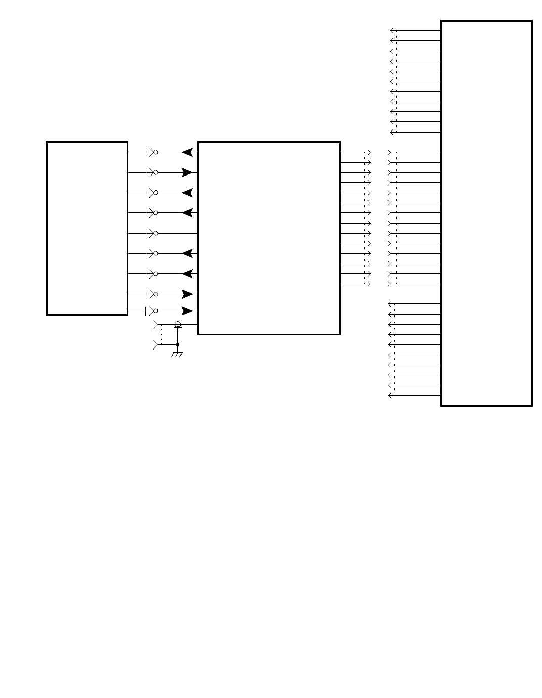
SCHEMATICS AND COMPONENT LAYOUTS
8-2
June 1997
Part No. 001-3412-002
Figure 8-1 3412 INTERCONNECT
DATA
GROUND
RSSI
MOD IN
SYNTH LOCK
SYNTH EN
CLOCK
DIAG EN
DEMOD
DIAG
GROUND
SYNTH LOCK
SYNTH EN
DATA
CLOCK
DEMOD
J201
WIDE BAND OUT
RSSI
AUDIO OUT
GROUND
AUDIO IN
CARRIER DETECT
PTT
WIDE BAND IN
12
11
1
2
3
4
5
6
7
8
9
10
13
14
MOD IN
DIAG EN
RSSI
DIAG
FREQ SEL
1
2
3
4
5
6
7
8
9
10
1
2
3
4
5GROUND
RX DATA
TX DATA
SLEEP/WAKE
CONNECTOR
PROGRAMMING
USER INTERFACE
LOADER BOARD
RF BOARD
J501
ANTENNA
VCO
W0855
W0854
W0859
W0856
W0852
W0851
W0854
CONTROL
GROUND
MODULATION
T/R PIN SHIFT
VCO OUT
PRESCALER RF OUT
+4.6V DC
-2.0V
VCO IN
T/R PIN SHIFT
MODULATION
GROUND
CONTROL
PRESCALER RF IN
+4.6V DC
-2.0V
J104
11
6
7
8
9
10 GROUND
GROUND
NC
PRG0
NC
PRG1
PRG2
J201
J102
+13.3V DC
+13.3V DC IN
TX EN
RX EN
RF EN
+13.3V DC SWITCHED
TX EN
RX EN
RF EN
023-3240-330
W0850
W0857 MODULATION ADJUST
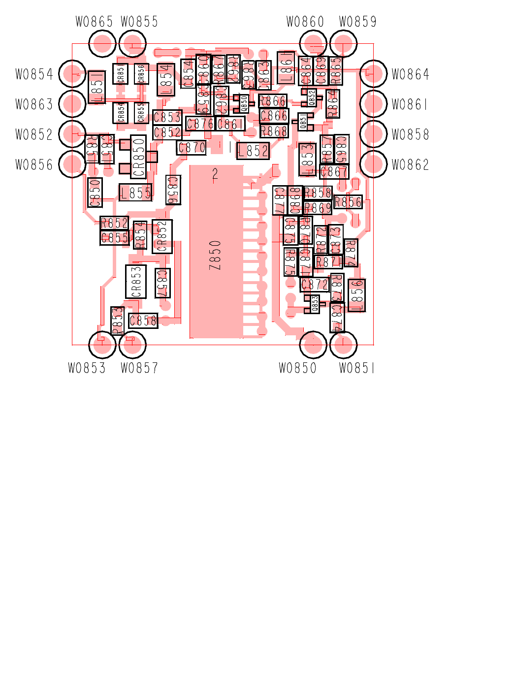
SCHEMATICS AND COMPONENT LAYOUTS
8-3
June 1997
Part No. 001-3412-002
Figure 8-2 VCO COMPONENT LAYOUT (COMPONENT SIDE VIEW)
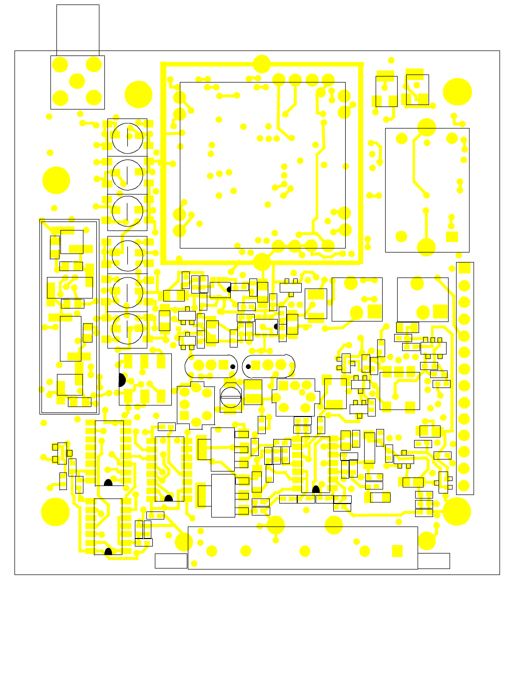
SCHEMATICS AND COMPONENT LAYOUTS
8-4
June 1997
Part No. 001-3412-002
Figure 8-3 TRANSCEIVER COMPONENT LAYOUT (COMPONENT SIDE VIEW)
L222
L553
L552
L551
L554
U211
C555
C556
C553
C554
C552
U912
U911
U913
Q124 Q531
L211
Z221 Z222
U111
U521
R533
R124
C122
C121 C123 R116
R536
C536
C221
L221
C125 +
R114
R113
R112
C113
C115
C101
C103
R102
C106
C104
C266
C261
R263
+
+
+
EP111
L253
R535
C102
C105
C114
C116
Q101
Q101
Q123
Q122
Q121
C535 C581
R521
R126
C123
C124
R534
R115
R111
C111
C112
R117
R913 C277
R255
J201
R911
R912
C911
R171 C172
C134
C136
C146
C144
R141 C133
+C171
C145
C135
+
+
+
+
C132
C141
U131
U141
Q131
R134
R133
C137
R131
R142
C142 C143
C131
Z252 Z251
U261
C268
R265
R264
C262
Y801
A801
VCO
TP831
R827
R825
Z201
Z202
J501
1
2 3
45
Q172
Q171
12345678910 11 12 13 14
R912
R914 R916
R915 Q911
R917
R823
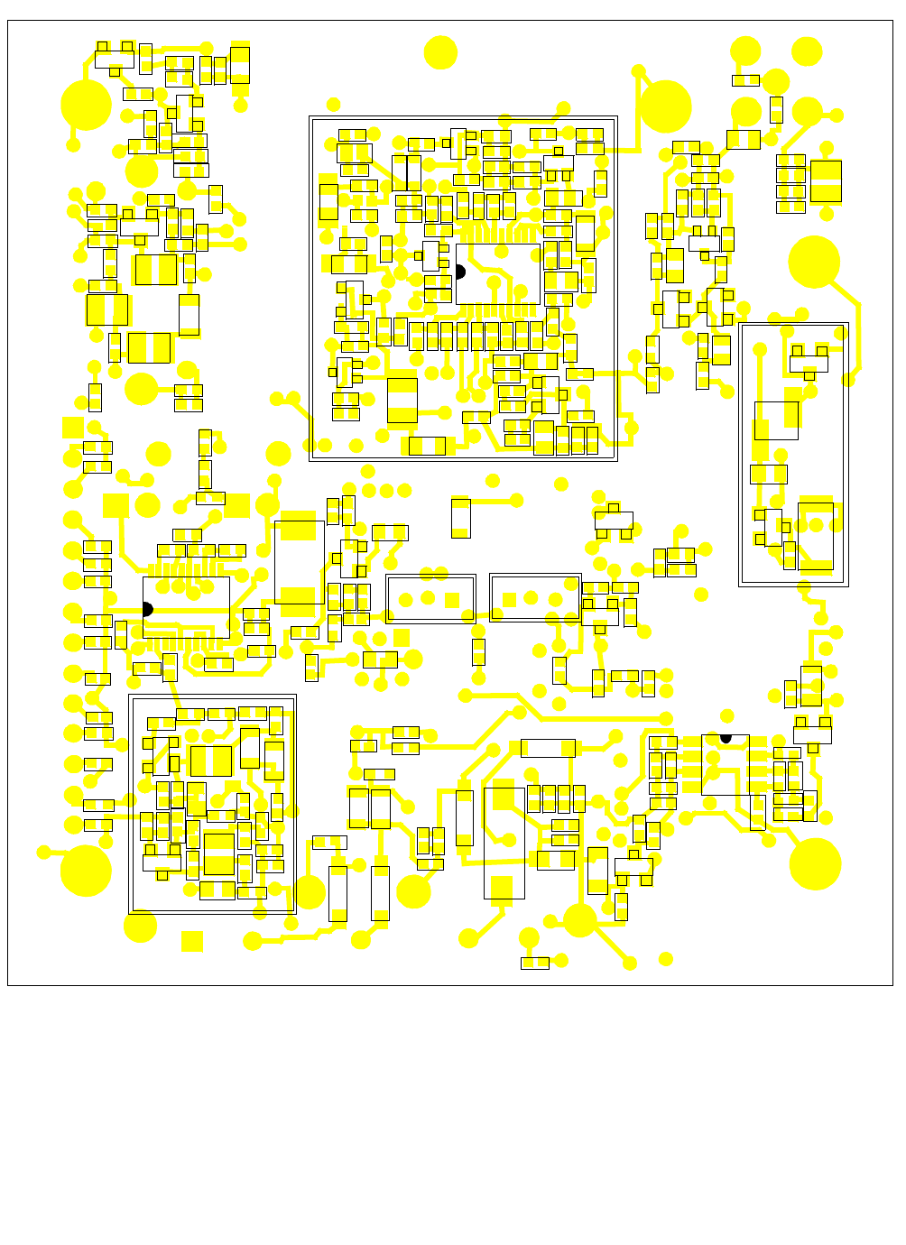
SCHEMATICS AND COMPONENT LAYOUTS
8-5
June 1997
Part No. 001-3412-002
Figure 8-4 TRANSCEIVER COMPONENT LAYOUT (OPPOSITE COMPONENT SIDE VIEW)
C707
CR701
Q401
Q701
L401
L402
L403
C708
C703
C701 R704
C702
R705
C704
C402
C404
R404
C405
C407
R401
R402
R403
C401
C403
R702
R701 C709
C706
+
C803
C406
C408
R801
C409
R703 R833 R843
C837
R821
R826
C804
C805
C806
R803
R804
R841
C848
C847
C846 C841
C845 C842
R842 C843
C844
R832
R831
R892
C362
R303
R302
C304
R304 C306
C307
C306
R301
C903
C902
R901
R802
C850
C849
C813
R817
R822
C822
R829
C825
R847
C815
C831
C816
C301
R893
R894
C812
C811
R816
R815
R813
R814
R812
R811
C309
C305
R305
+
C821
C836
C833
C303
L301
L302
C832
C832 +
+
Q901
Q801
Q842
Q841
L811
Q301
U811
CR901
CR562
CR231
Q202
Q201
C561
L202
L201
L555
L561
CR561
R565
C205
C544
C543
C542
C541
C202
C201
C209 C203
C204
R205
C208
C207 C206
R204 C210
R201
R202
R203
C562
C564
C563
R561
R593
C596
C584
C585
C593
R586
C583
C582
R592
C591
C595
R581 R584
C594
R594
R583
C592
C551
C521
C532
C508
C507
C506
C505
R591
CR592
CR591
U581
Q211
EP501
EP533
+
C522
EP531
EP534
EP532
C223
R121
R122
R206
C215
R213
C214
R211
R208
C213
C211
C212
R212
C222
C534
R574
R573
C582
C533
C523
C524
C531
R132
C233
Q231
R235
C235
C232
R261
C266
C265
C275
R234
R233
R232
R231
C231
C234
+C264
U241
R262
C279
C276
C271
C272
R272
C153
C154
C155
C156
C157
C158
C159
C160
C161
C162
C163
C501 R503 R502 R501
R511
C513
C514
C518
R505
R504
L511
L513
L512
L501
Q511
Q501
C503
C502
C511
R513
C516
C517
R514 C515
R512
C519
R515
C504
C512 C267
R275
C152
C151
C801
C802
R271 C273
Q173
Q302
R902
R903
+
C826
C827

SCHEMATICS AND COMPONENT LAYOUTS
8-6
June 1997
Part No. 001-3412-002
This page intentionally left blank.

SCHEMATICS AND COMPONENT LAYOUTS
8-7
June 1997
Part No. 001-3412-002
REVISED
Figure 8-5 SCHEMATIC (1 OF 2)

SCHEMATICS AND COMPONENT LAYOUTS
8-8
June 1997
Part No. 001-3412-002
REVISED
Figure 8-6 SCHEMATIC (2 OF 2)