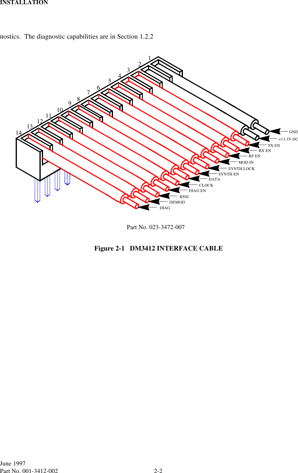
CalAmp Wireless Networks 2424046-001 T-96SR UHF Telemetry Transceiver/Modem User Manual Cover dmf
CalAmp Wireless Networks Corporation T-96SR UHF Telemetry Transceiver/Modem Cover dmf
UserManual.wiki
>
CalAmp Wireless Networks
>
2424046-001 User Manual
>
Transceiver Manual
Contents
1.
Transceiver Manual
2.
Modem Manual
Transceiver Manual
Navigation menu
Upload a User Manual
Namespaces
Wiki Guide
HTML
PDF
Info
Views
User Manual
Discussion / Help
Navigation
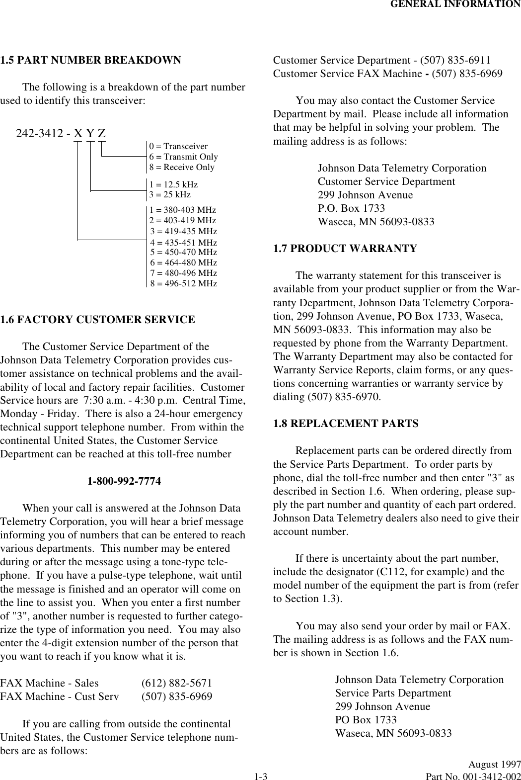
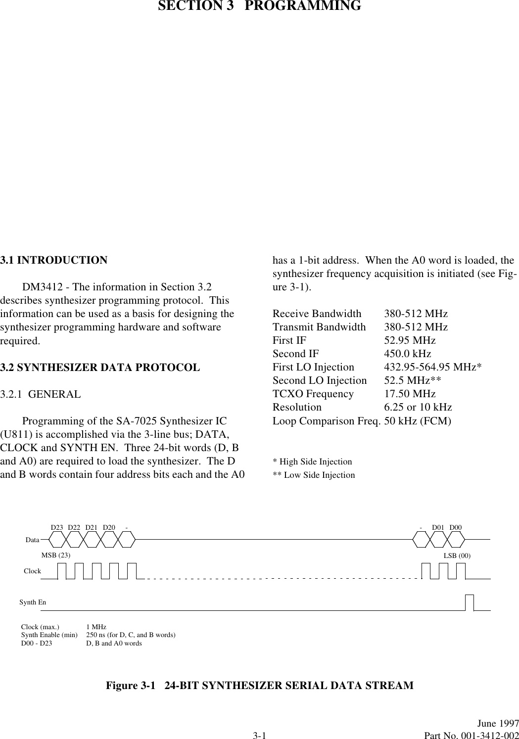
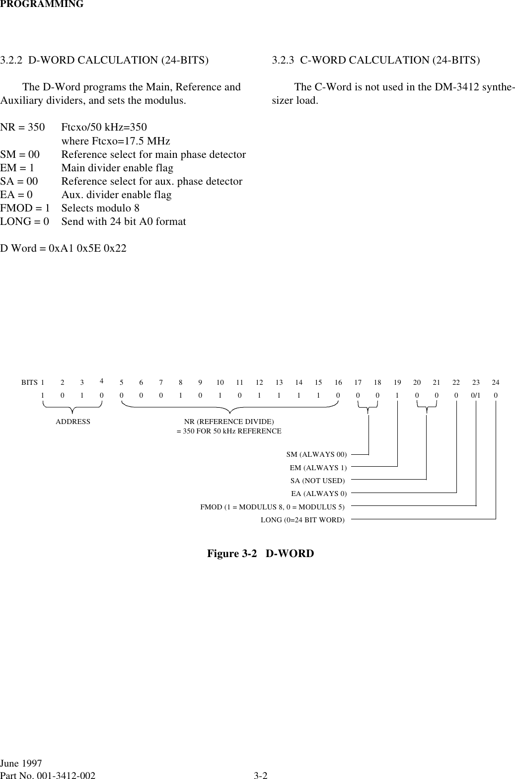
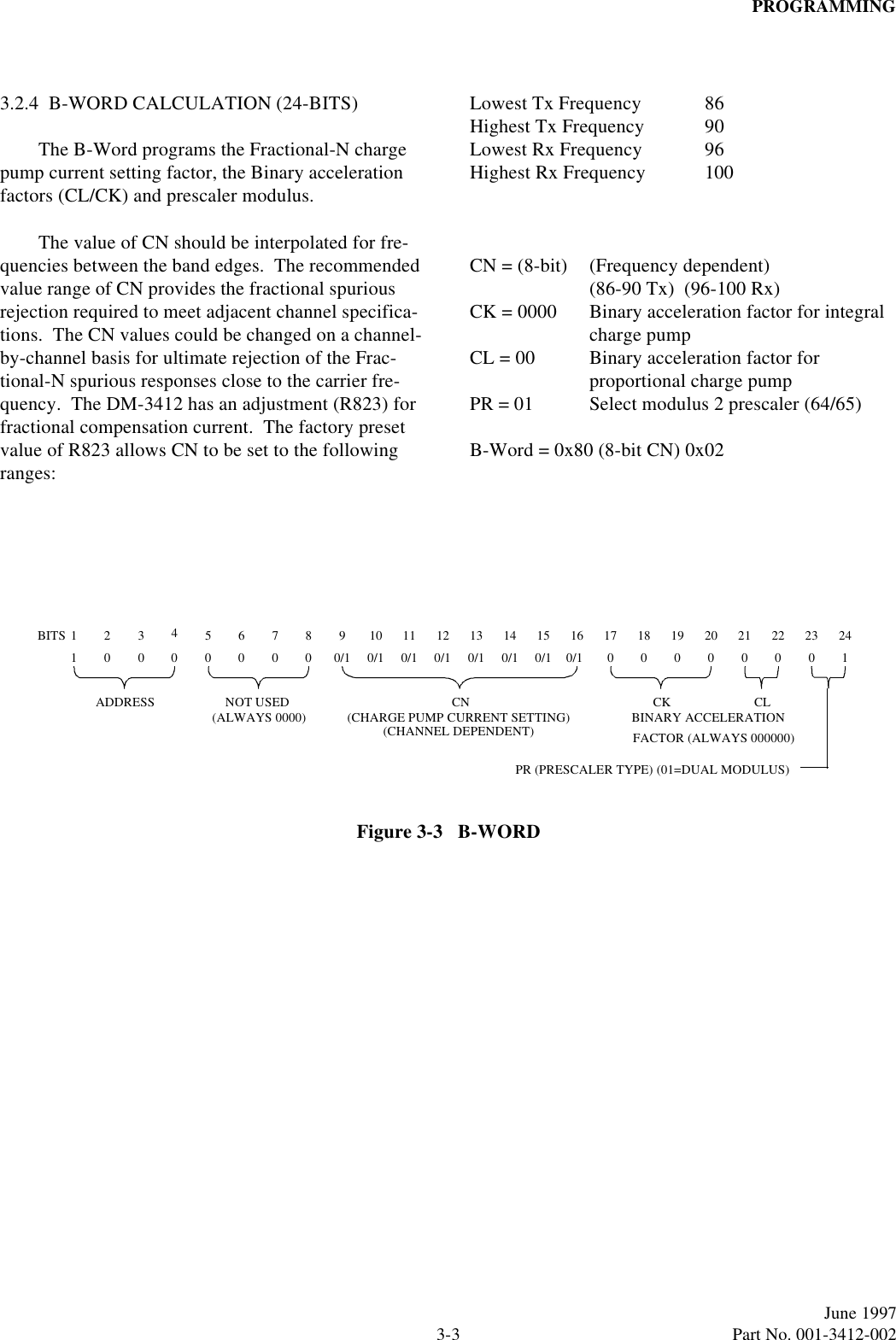
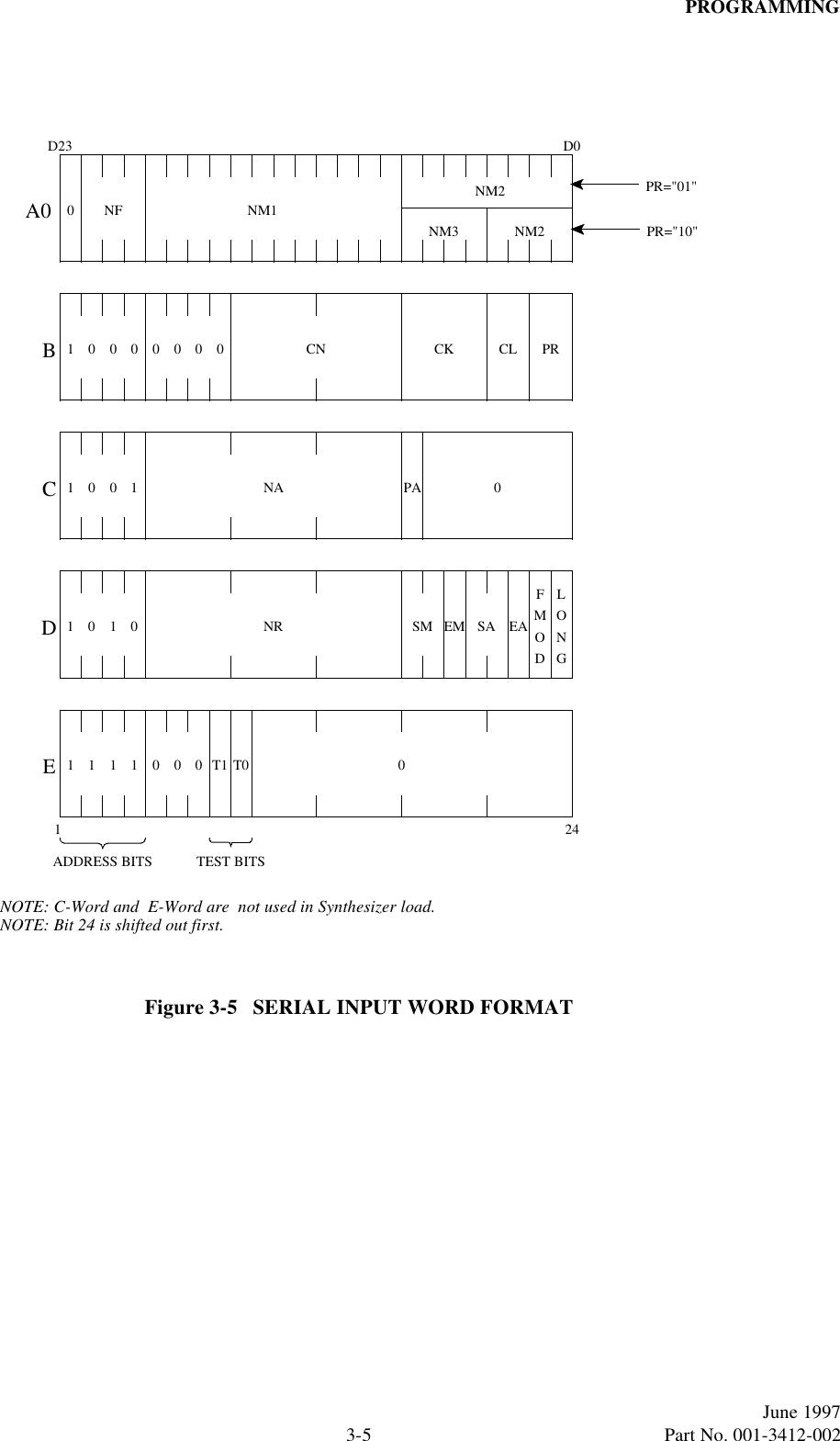
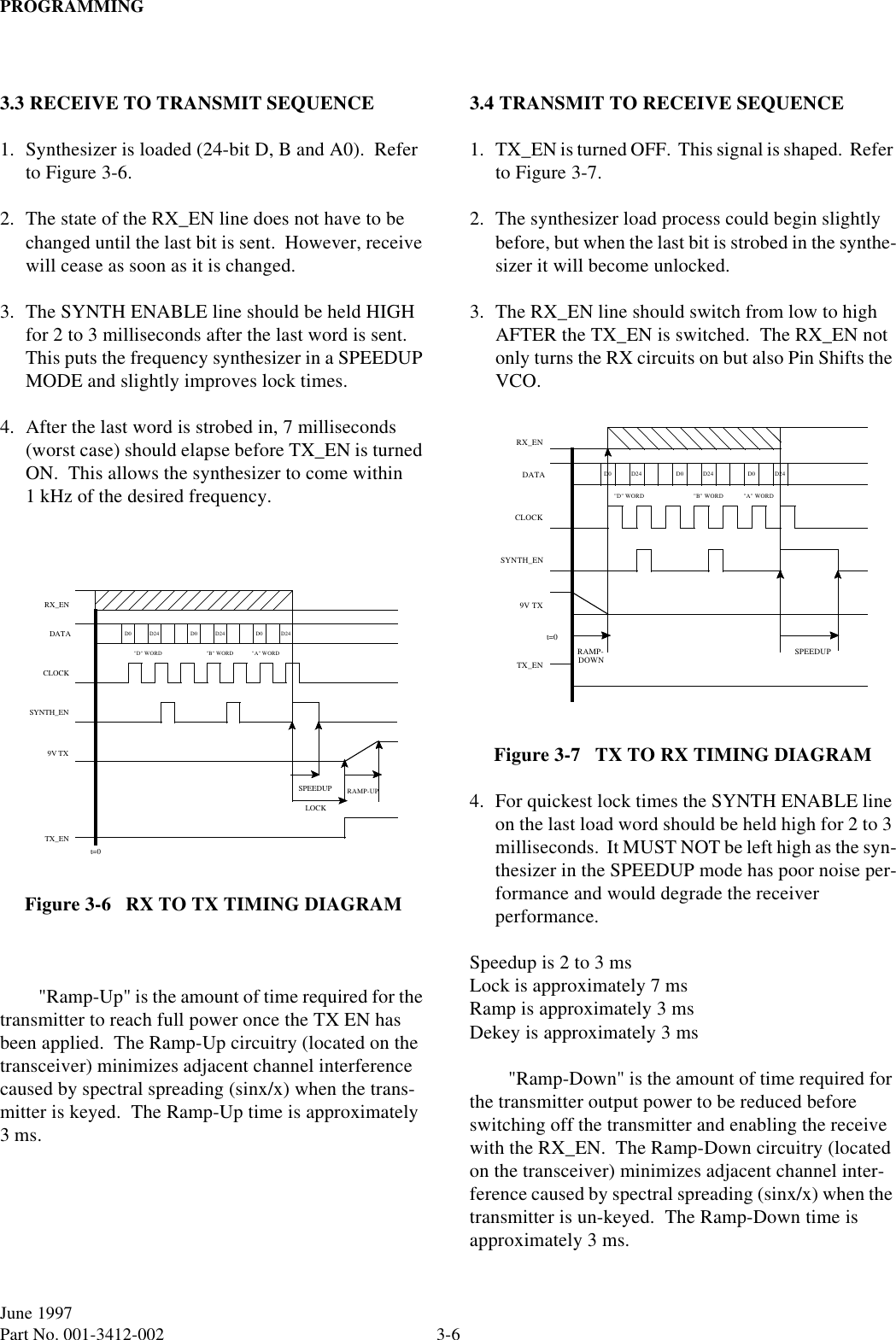
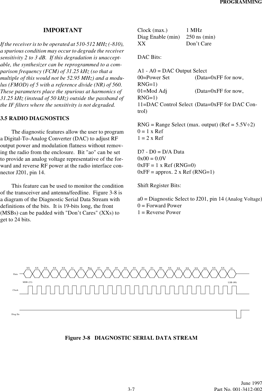
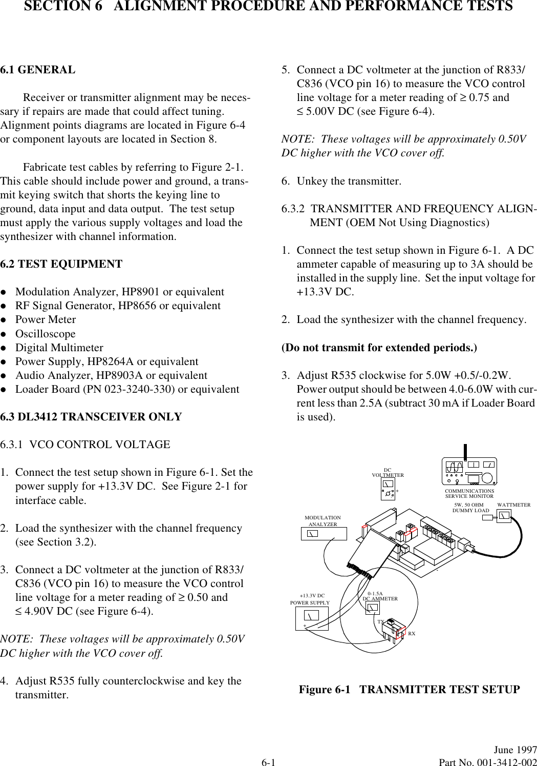
![PROGRAMMING3-4June 1997Part No. 001-3412-002 3.2.5 A0-WORD CALCULATION (24-BITS)The A0-Word is sent last (see Figure 3-4). The A0-Word contains the data for the loop dividers and is programmed on a channel-by-channel basis. The Fractional-N (NF) word is a 3-bit word that programs the synthesizer to the fractional steps determined by the fractional modulus selection flag FMOD (1 = modulus 8) and the loop comparison frequency (50 kHz). The frequency resolution is:50 kHz ÷ 8 = 6.25 kHz.NF= (3-bits)* Fractional increment for modulus 8 (3-bits)NM1=(12-bits)* Number of main divide cycles when prescaler modulus equals 64 (12-bits)NM2=(8-bits)* Number of main divide cycles when prescaler modulus equals 65 (4-bits, PR=01)NM3=(4-bits)* Number of main divide cycles when prescaler modulus equals 72 (4 bits, PR=10) NOTE: NM3 is not used because dual modulus is selected by PR=01.* Indicates frequency/channel dependant variable.The Fractional-N increment (NF) is a 3-bit word that is channel dependant. NF is used to program the synthesizer to channels (frequency steps) that are below the comparison frequency (FCM), i.e. frequen-cies that are not divisible by FCM. When the D-word is programmed with FMOD = 8, and NR = 350 as described in Section 3.2.2, the fractional increment is: 50 kHz ÷ 8 = 6.25 kHz.FCM = Ftcxo ÷ NR = 17.5 MHz ÷ 350 = 50 kHzThe synthesizer resolution (min. step) is 6.25 kHz.Example Calculation: Program the transceiver to receive at 457.01875 MHz:RX = 457.01875 MHzLO = RX + 52.95 MHz = 509.96875 MHz (LO is high-side injection)N = LO ÷ FCM = 509.96875 ÷ 0.05 = 10199 (integer)NM2 = 64 x FRAC [N ÷ 64] = 64 x FRAC [10199 ÷ 64]= 64 x 0.359375= 23NM1 = INTEGER [N ÷ 64] - 2 - NM2 = 159 - 2 - 23= 134NF = 18.75 kHz ÷ 6.25 kHz = 3NOTE: Channel steps of 10 kHz can also be achieved by setting the Fractional-N modulus flag (FMOD) in the D-word to "0" which sets FMOD to 5. NR remains set to 350. This produces 10 kHz steps as NF is incremented.Figure 3-4 A0-WORD4321 141312111098765 2019181715 16 24232221ADDRESSBITS0/1 0/1 0/1 0/1 0/1 0/1 0/1 0/10NF0/10/10/10/1 0/1 0/1 0/1 0/1 0/1 0/1 0/1 0/1NM1(NUMBER OF MAIN DIVIDER CYCLESWHEN PRESCALER MODULUS = 64)(NUMBER OF MAIN DIVIDER CYCLESNM2WHEN PRESCALER MODULUS = 65)0/10/10/1](https://usermanual.wiki/CalAmp-Wireless-Networks/2424046-001.Transceiver-Manual/User-Guide-6856-Page-17.png)