California Eastern Laboratories WB4343WF3SP2 WiFi/Bluetooth/Bluetooth Smart Mini Module User Manual MeshConnect
California Eastern Laboratories WiFi/Bluetooth/Bluetooth Smart Mini Module MeshConnect
UserManual.wiki
>
California Eastern Laboratories
>
WB4343WF3SP2 User Manual
Exhibit D Users Manual per 2 1033 b3
Navigation menu
Upload a User Manual
Namespaces
Wiki Guide
HTML
PDF
Info
Views
User Manual
Discussion / Help
Navigation
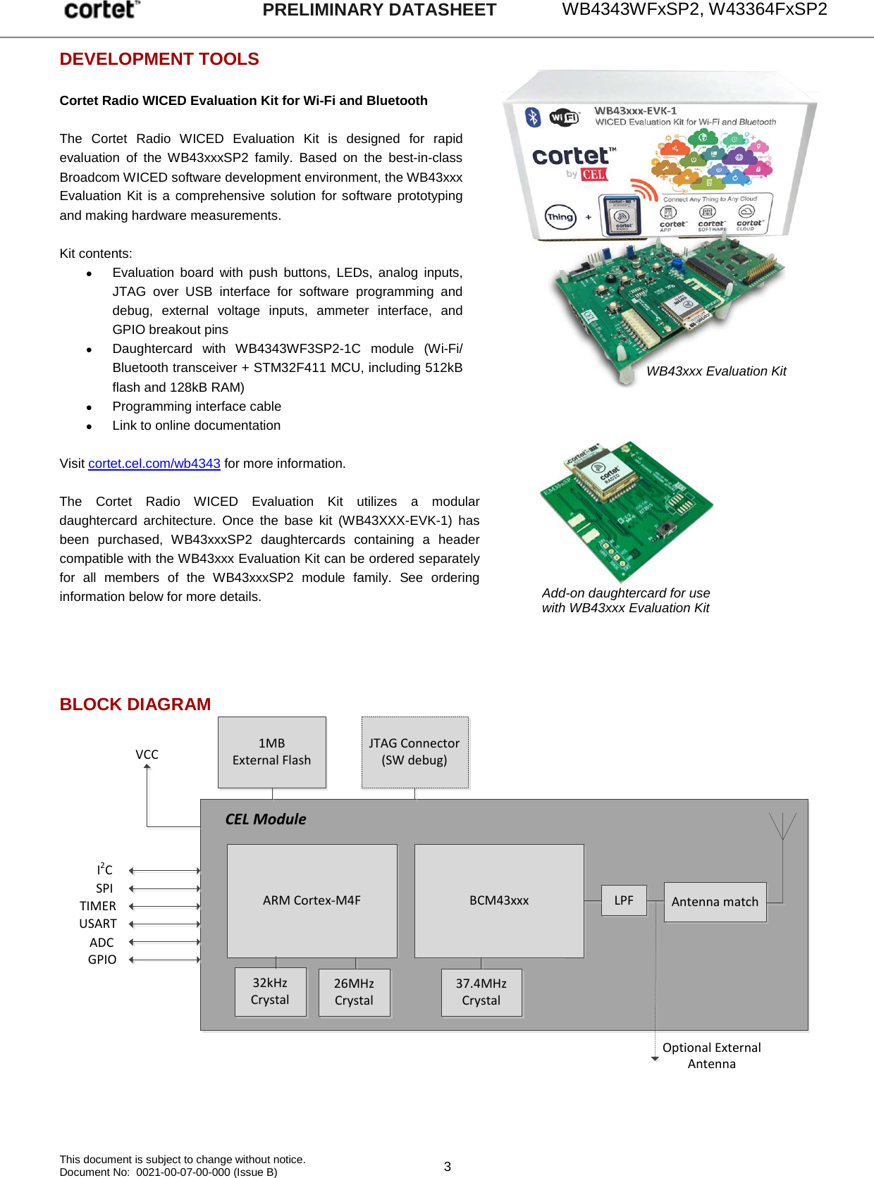
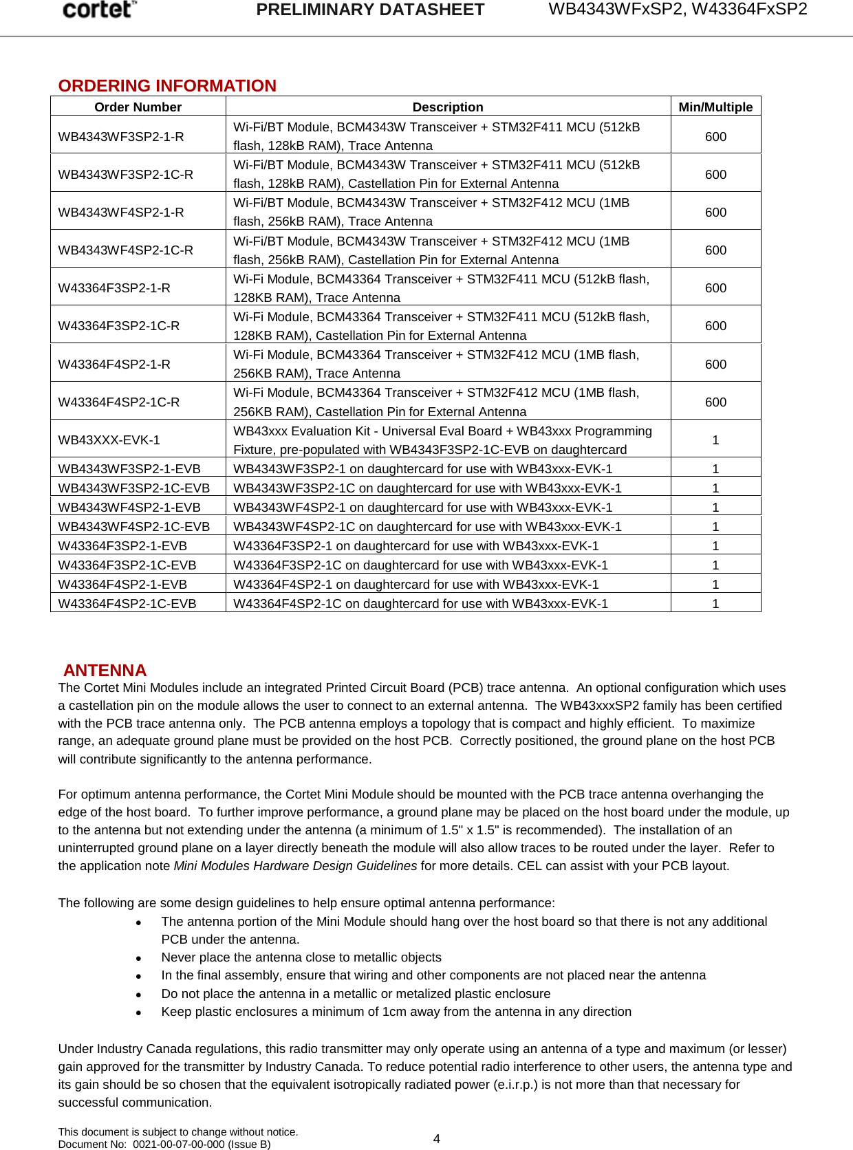
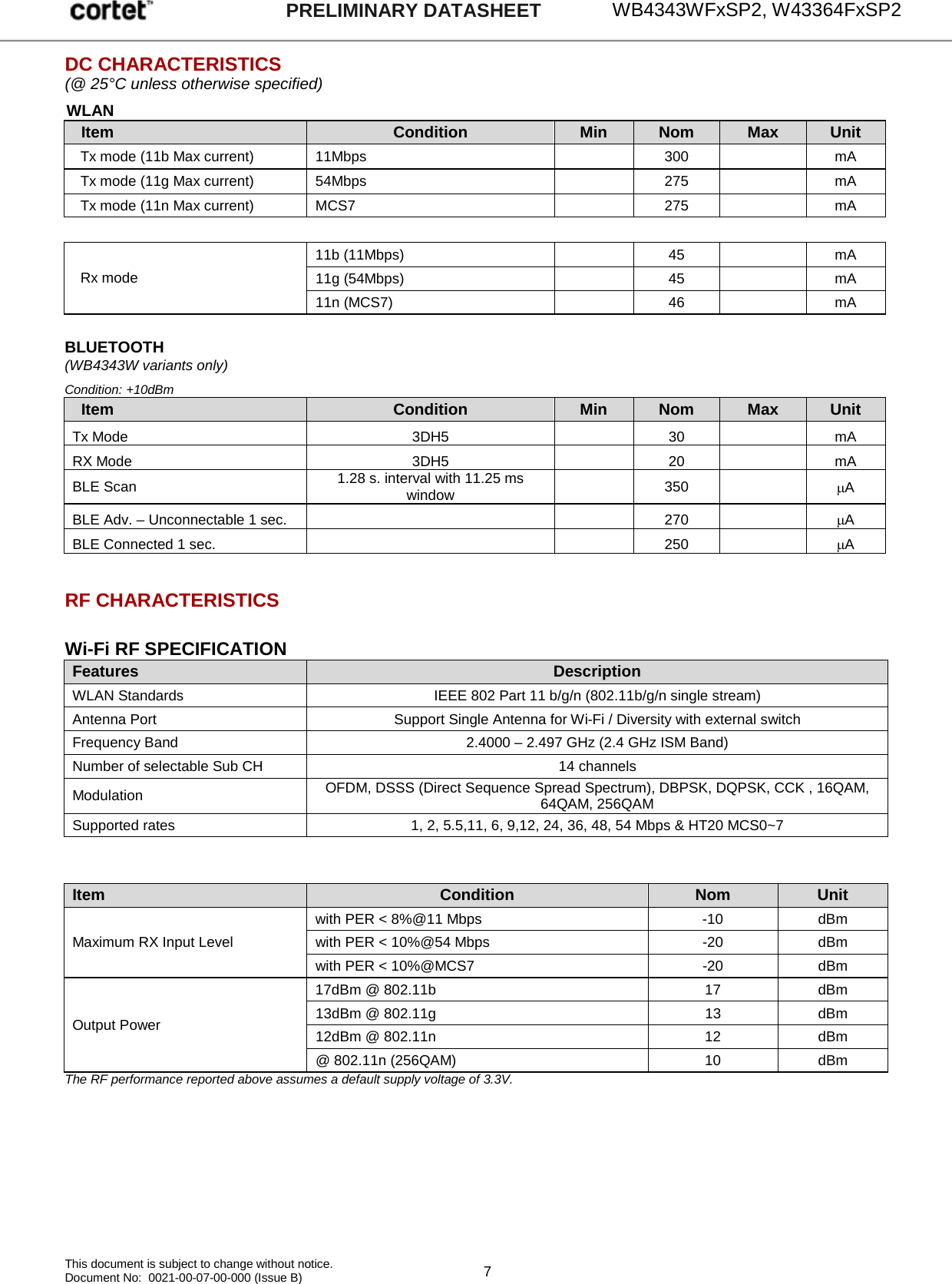
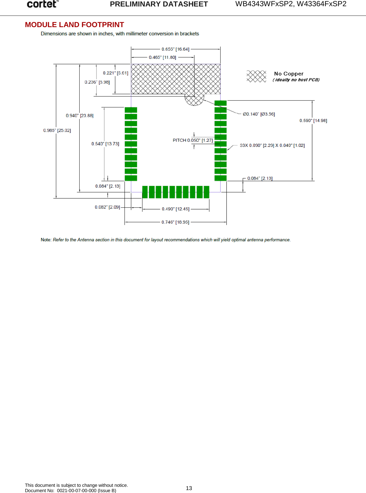
![WB4343WFxSP2, W43364FxSP2 This document is subject to change without notice. Document No: 0021-00-07-00-000 (Issue B) 12 PRELIMINARY DATASHEET CEL MINI MODULE COMPATIBILITY The geometry of the land pattern and location of the RF castellations is identical to CEL’s ZICM35x family of ZigBee/Thread and B1010 Bluetooth Smart Mini Modules. The digital and analog mapping to develop a drop-in compatible solution is described below: Pin # Function ZICM35x B1010 WB43xxx Notes 4 Reset RESET N/C RESET 5, 6 Low frequency crystal PC6, PC7 N/C N/C Low frequency crystal is internal for B1010 and WB43xxx 7 Wake PA7 WAKE PA0 8, 9, 19, 20 Serial Controller 1 UART/SPI/I2C Two wire UART/I2C USART/I2C 10, 11, 14, 15 Serial Controller 2 SPI/I2C I2C SPI/I2C 16, 17, 21, 22, 23, 24, 27 Programming Programming Programming Programming 28, 30 ADC PB7, PB5 AIO[1], AIO[2] PA3, PA1 29 Timer PB6 PIO[11] PA2 MODULE DIMENSIONS](https://usermanual.wiki/California-Eastern-Laboratories/WB4343WF3SP2/User-Guide-3078185-Page-12.png)