Cambridge Silicon Radio BSMAN BlueSlim Modules BSMAN1, BSMAN3 and BSMAN4 User Manual Antenna 2
Cambridge Silicon Radio Ltd BlueSlim Modules BSMAN1, BSMAN3 and BSMAN4 Antenna 2
Contents
Antenna 2
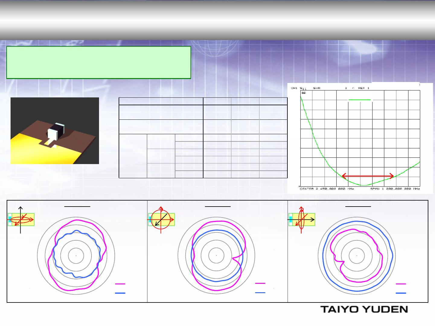
2400MHz 2450MHz 2500MHz
Efficienc
y
[dB] -1.6 -1.5 -1.5
( 69%) ( 70%) ( 71%)
Peak gain [dBi] 1.5 1.5 1.8
Average XY-plane TX-H -3.0 -2.8 -2.9
gain TX-V -15.1 -15.2 -15.0
[dBi] YZ-plane TX-H -2.8 -2.9 -3.2
TX-V -11.5 -11.4 -11.1
ZX-plane TX-H -12.0 -11.8 -11.4
TX-V 0.0 0.0 0.1
XY-plane YZ-plane ZX-plane @2450MHz
(-X) (+Z) (+Z)
(-Y) (+Y) (-Y) (+Y) (+X) (-X)
unit: dBi (+X) (-Z) (-Z)
-45
-35
-25
-15
-5
5
TX-H
TX-V
+Y
+X
+Z
+Y
+X
+Z
+Y
+X
+Z
-45
-35
-25
-15
-5
5
TX-H
TX-V
-45
-35
-25
-15
-5
5
TX-H
TX-V
Bandwise: 440MHz
(VSWR<2)
Efficiency > -1.6dB (69%)
Peak Gain > +1.7dBi
Average Gain > +0.0dBi (ZX plane-Vertical polarization)
■Radiation Pattern
■Electrical Characteristics
VSWR
Element-GND Distance: 3.5mm
2.5 x 1.6 x 1.6 mm
■Shapes
*on Taiyo Yuden’s Evaluation Board
*GND size on evaluation board: 45x10mm
2.4GHz Helical Antenna
2.4GHz Helical Antenna : AF 216M245001
: AF 216M245001
No.1 Small Size : The Smallest Size in the world in keeping high efficiency
Confidential
Confidential
-1-
−2−
1.0 Scope
This specification covers the helical antenna in mounted condition on Taiyo Yuden evaluation board.
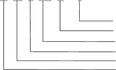
Part Numbering System
AF 216 M 2450 01 − T
2.0 Environment condition (Refer to the reliability test of table -1 for the reliability assurance)
2.1 Operating temperature range : -20℃ to +80℃
2.2 Humidity : 15 to 95%RH (Without dew condensation)
2.3 Storage temperature range(Antenna of single unit)
: -40℃ to +85℃
2.4 Storage temperature and humidity range (packing condition)
: -10℃ to +40℃, 15 to 85% RH
3.0 Electrical characteristics
3.1 Input Impedance : 50Ω(Specified value )
3.2 Frequency bandwidth : 2400 to 2500MHz
3.3 Gain*1 : +1 dBi min. (Peak)
: -2 dBi min.
(Vertical polarization average gain of omni directional plane)
: -6 dBi min. (Total average gain)
3.4 VSWR in bandwidth*2 : 3.0 (Typical)
*1: Total average gain in 3.3 of electrical characteristics shall be total average gain of V, H polarization in X-Y,
Y-Z and X-Z side (Average of total measurement points) in mounted on Taiyo Yuden evaluation board.
*2: VSWR in bandwidth in 3.4 of electrical specification shall be VSWR mounted on Taiyo Yuden on standard
board.
4.0 Mechanical performance
4.1 Shape dimension: Refer to figure -1.
4.2 Dimension of evaluation board and land-patterns: Refer to figure -2, 3.
Package (T: Taping)
Individual specification
Frequency bandwidth (4-digit number in MHz)
Size (mm)
Antenna Class
Type
−3−
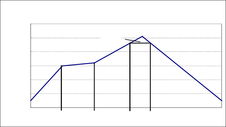
Reflow soldering temperature profile
Recommended reflow profile
0
50
100
150
200
250
300
About 60s 55∼75s 20∼30s
Temp
(℃)
230℃ Peak temperature: 250∼255℃
Time(sec)
−4−
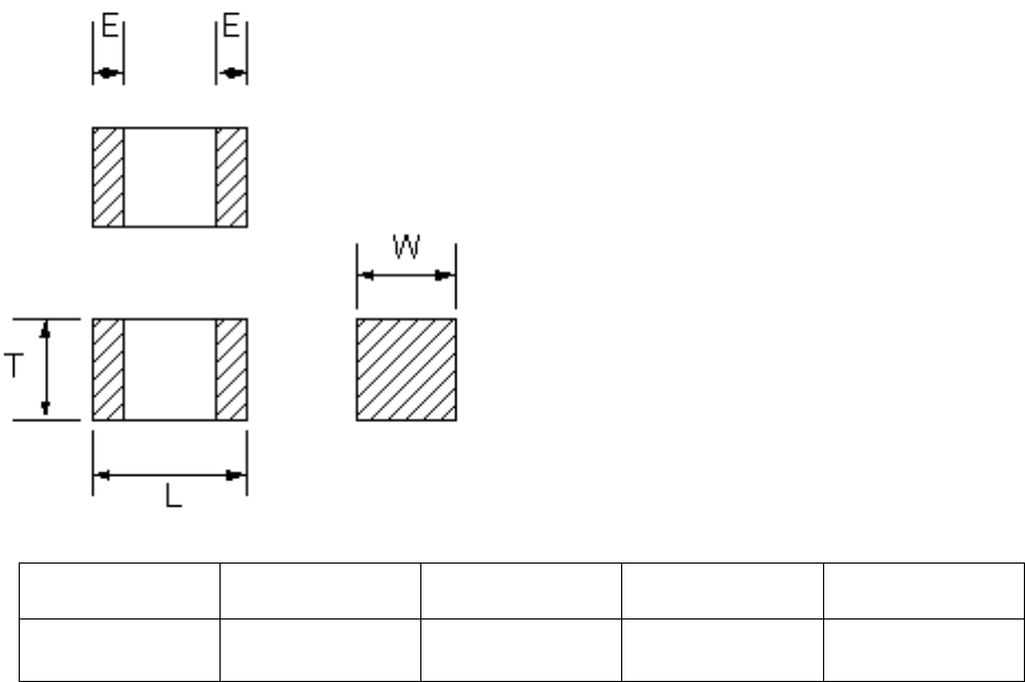
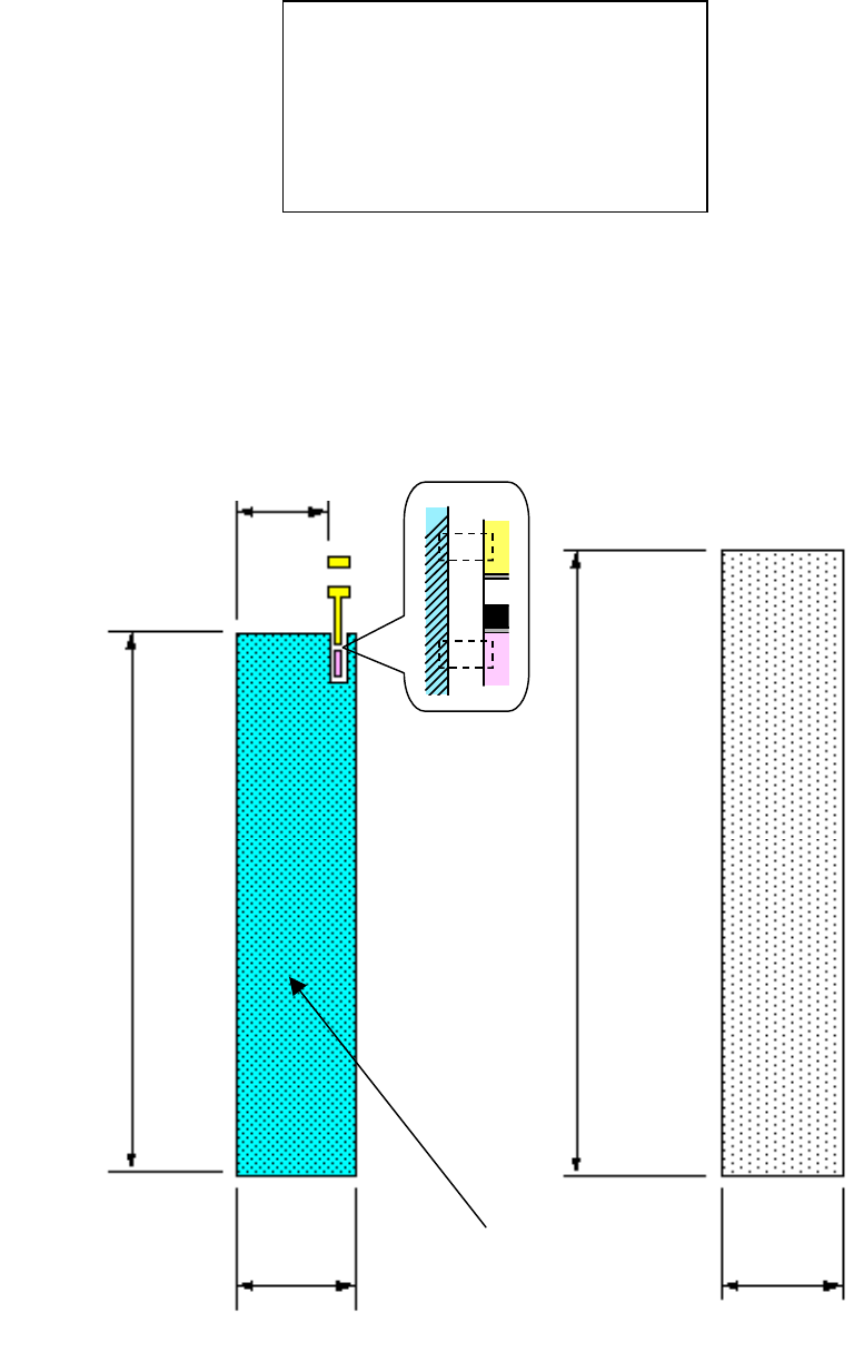
Figure -1
Part number: PG_AF_216M245001-T
Shape dimension
Code L W T E
Size 2.5±0.2 1.6±0.2 1.6±0.2 0.5±0.3
Unit:mm
−5−
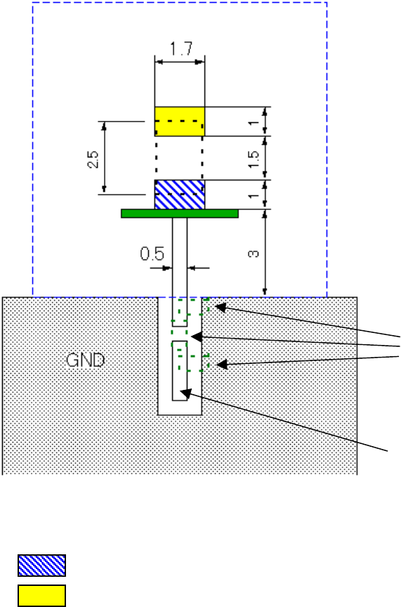
Figure -2
Dimension of evaluation board for this antenna
pattern Board size
・Board material: FR-4
・Thickness of base material: 0.8mm
・Electrode pattern: single-side
・Thickness of electrode: 35μm
・Land part: Refer to figure3
7.8
45
52
10 10
Matching circuit
HK1005 6N8J (6.8nH)
Unit:mm
Ground pattern
−6−
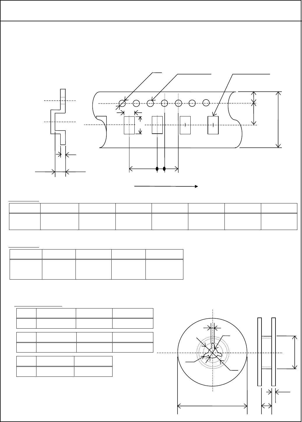
Figure -3
Antenna land-patterns (Tentative)
※1:Don't arrange the pattern on near, surface and inside layer to the antenna mounting area.
(Refer to our company evaluation circuit board.)
※2:A solder area is set at solder resist.
Land for input terminal
Land for NC terminal
50Ω input
Land for matching circuit
(1005 chip)
Unit:mm
※
2
※
1
−7−
Precautions
1.Be careful of using these products because characteristics may be deteriorated when it is used in the
following environment.
・Special gas atmosphere (Such as CI2, NH3, SOx and Nox, etc.)
・Gas atmosphere with volatility and flammability
・Place where dust is abundant
・Place where water splashes directly, dew condensation is ease to occur because of high humidity, direct
sunlight is subjected and freeze.
2.Don’t apply excessive pressure and shock because these products are made from ceramics element.
3.Don’t apply excessive pressure and shock to these products during transporting and handling of print circuit
board that these products are soldered.
4.Be careful of handling (Don’t fall and hit) because characteristics changes when electrode is damaged and
chipped out. And, don't touch these products with bare hands because it causes a solderability decline.
5.Please storage under the following condition
Temperature : Below +40 ℃
Humidity : Below 85% RH
Use these products after the delivery within six months. And, after more than six months have passed,
confirm solderability before the use them.
6.Arrange these products of position of mounting where stress isn't applied against sled and deflection of circuit
board.
Be careful not to apply stress and deflection of board during process after soldering these products (circuit
board cut, break board checker, mounting of other components, installation to chassis and wave soldering
to backside of the circuit board after Reflow soldering) because electrode peeling and chip break occur by
stress and deflection. When separating print circuit board after mounting, please 7.Be careful not to apply
excessive stress and shock to prevent break and chip out during mounting these products on print circuit
board.
8.Please use flux containing less than 0.1% wt (cl conversion) of halogen material in soldering to prevent
corrosion of electrodes and decline of insulation resistance.
9.Preheat in soldering so as to be less than 100℃ between solder temperature and products temperate to
prevent break of these products.
10.When supersonic washing is applied, please confirm cleaning condition in advance because crack may occur
in these products and the soldering part by vibration and strength of the terminal electrode may be declined.
11.When repairing by hand solder iron, temperature of soldering iron should be less than less than 320℃ for less
than 3 seconds to prevent a terminal electrode decline.
−8−
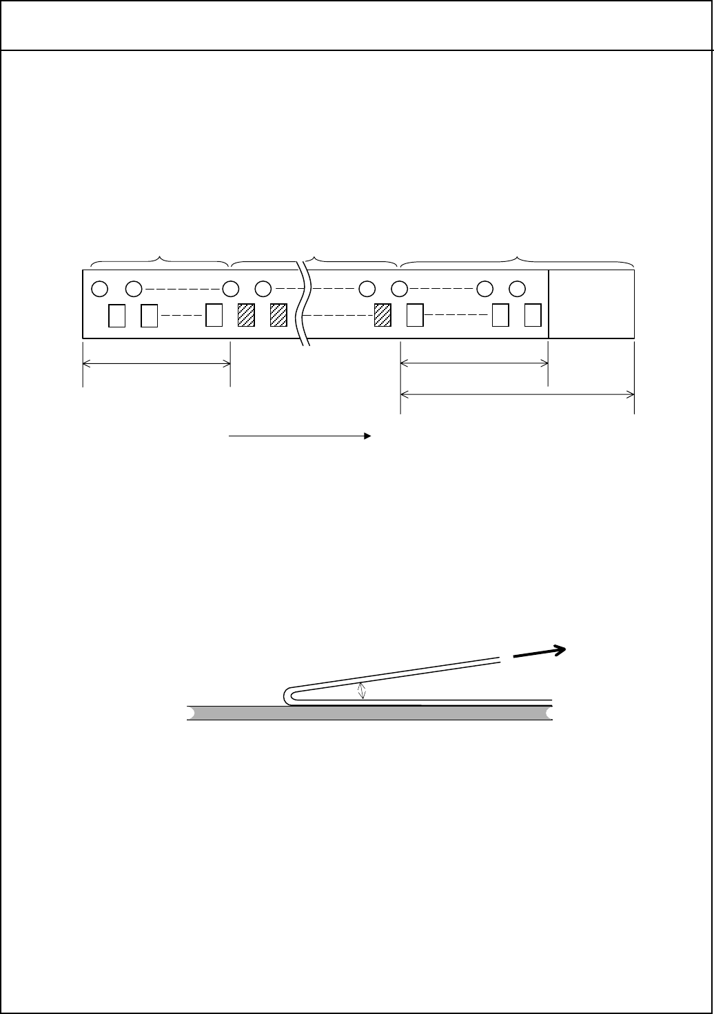
◎In case of taping packing, plastic tapes shall be used.
Dimensions
Code A B C D E F G
Size 1.85±0.1 2.75±0.1 8.0±0.2 3.5±0.05 1.75±0.1 4.0±0.1 2.0±0.05
[Unit:mm]
Dimensions
Code H J K t
+0.1
Size 4.0±0.1 φ1.5 −0 1.85 max. 0.25 max.
※A, B, t:Sufficient clearance. [Unit:mm]
Dimension of Reel Dimensions of Reel
Code A B C
Size φ178±2.0 φ50 min. φ13.0±0.2
Code D E W
Size φ21.0±0.8 2.0±0.5 10±1.5
Code t R
Size 3.0 max. 1.0
[Unit:mm]
Tape Packaging (T)
B
t
W
C
E
D
R
A
Feeding direction
Tape Size
Plastic tape
C
E
D
JSprocket hole
F
Chip cavity
Feeding direction
A
B
GH
Tape Size
t
k
−9−
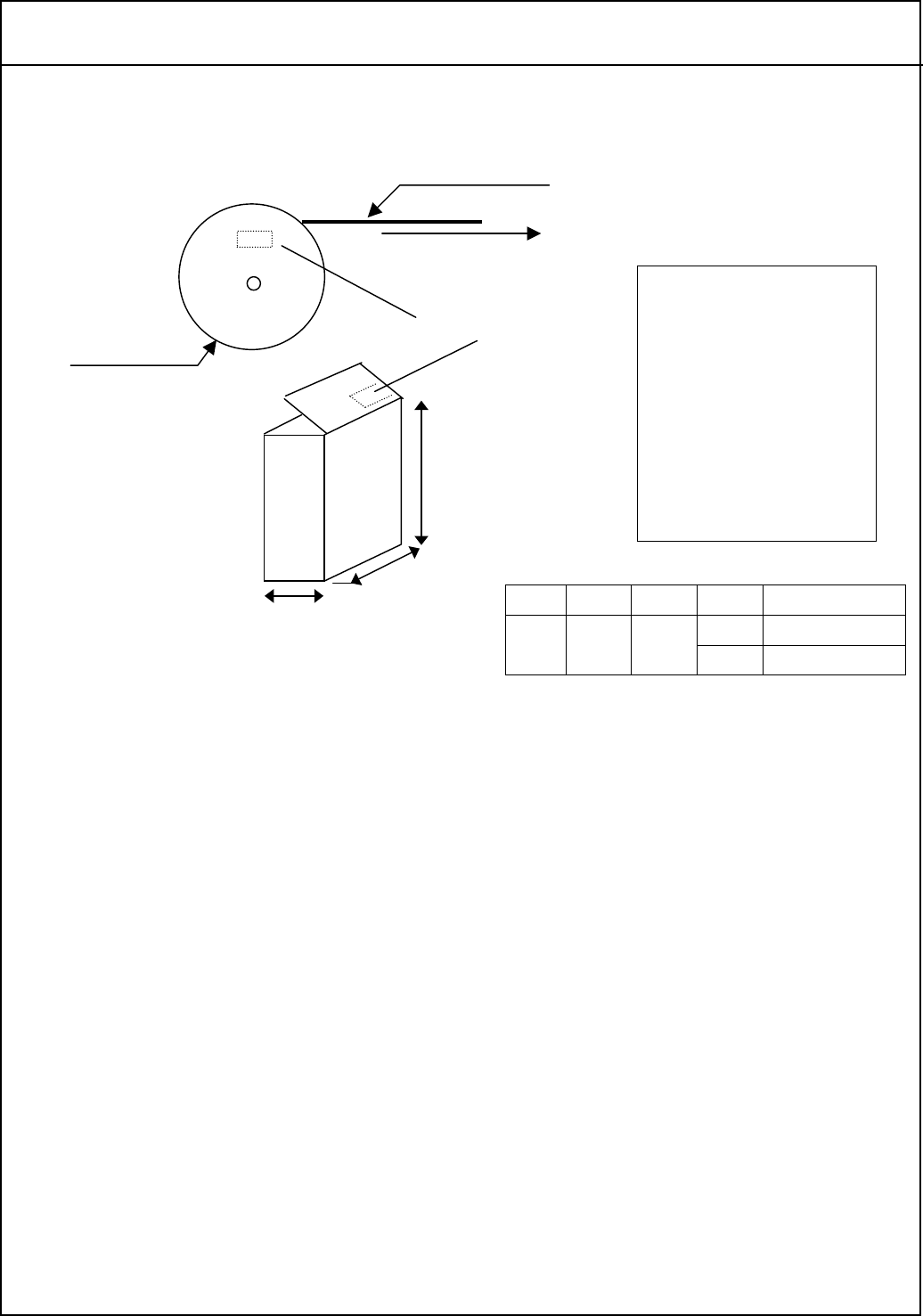
1. Taping shall be right-sided wound. When the end is pulled out, sprocket hole will be at the
right-hand side.
2. For packaging chips by taping, blank spaces are provided on taping as shown in the figure.
・Leader part 400mm min.
・Leader part (Blank part) 20 pockets min.
・Trailer (Blank part) 40 pockets min.
3. Seal tape of plastic taping shall not be crossed over sprocket holes.
4. Plastic tape shall not be seamed.
5. Tensile strength of tape is 5N (0.51kgf) or over.
6. Number of chips missed from tape reel shall be 1 piece maximum per reel.
7. Standard number of chips contained in a reel shall be 2,000 pieces.
8. Label indicating part No., quantity and control No. shall be attached to the outside of reel.
9. Peeling strength of seal tape (or top tape) shall be 0.1∼0.7N (10.2∼71.4gf) when seal tape (or top tape)
is peeled from carrier tape at an angle of 0°∼ 20°.
Tape Packaging (T)
Trailer Chip packaging area Leader part
End
Blank part
No shorter than 40 pockets
Blank part
No shorter than 20 pockets
No shorter than 400mm
Feeding direction
Start
0
∼2
0
°
−10−
[Packaging Mode]
Code A B C Reel
70 5 reels max.
Size 190 185 140 10 reels max.
[Unit: mm] (The size is only for reference.)
Material: Paper
Packaging unit: Maximum 5 reels or 10 reels in a box.
・To attach labels means that all products are passed.
Tape Packaging (T)
Feeding direction
Customer label
Tape packaging
Reel
Customer label description
1.Manufacturer Name
2.Customer Parts No.
3.Our Parts No.
4.Quantity
5. Control No.
(Shipping Lot No.)
6.Manufacturing site
(MADE IN ○○○)
B
A
C

−11−
Operating conditions for guarantee of this product are as shown
in the specification.
Please note that Taiyo Yuden Co., Ltd. shall not be responsible
for a failure and/or abnormality which are caused by use under
the conditions other than the aforesaid operating conditions.
This product is developed, designed and intended for use in general electronics equipments. (for AV, household,
office supply, information service, telecommunications, etc.). Before incorporating the components into any
equipments in the field such as aerospace, aviation, nuclear control, submarine, transportation, (automotive
driving and control, passenger protection, train control, ship control), transportation signal, disaster prevention,
medical, public information network etc.
where higher safety and reliability are especially required, please contact Taiyo Yuden Co., Ltd. for more detail in
advance.
And before incorporating the components or devices into the equipments not mentioned in the above, if there is
possibility of direct damage or injury to human body, please contact Taiyo Yuden Co., Ltd. for more detail in
advance.