Casio Electronic Keyboard Ctk 530 Users Manual S/M
CTK-530 to the manual d22b8b53-5629-43a4-b02d-5636b997bc96
2015-01-21
: Casio Casio-Casio-Electronic-Keyboard-Ctk-530-Users-Manual-243273 casio-casio-electronic-keyboard-ctk-530-users-manual-243273 casio pdf
Open the PDF directly: View PDF ![]() .
.
Page Count: 18
- ÿþ�C�T�K�-�5�3�0
- ÿþ�C�O�N�T�E�N�T�S
- ÿþ�S�P�E�C�I�F�I�C�A�T�I�O�N�S
- ÿþ�B�L�O�C�K� �D�I�A�G�R�A�M
- ÿþ�C�I�R�C�U�I�T� �D�E�S�C�R�I�P�T�I�O�N
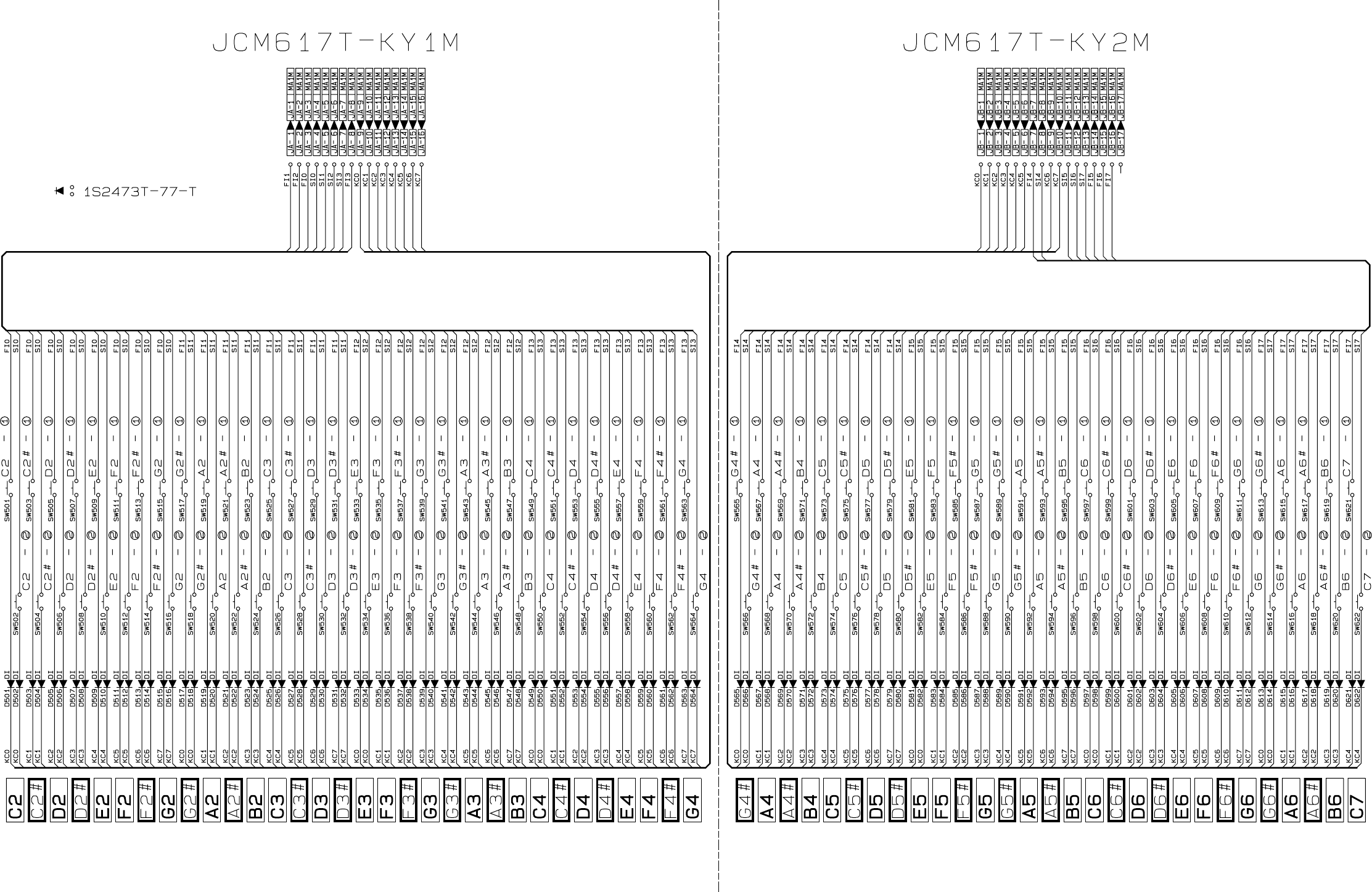
- ÿþ�K�E�Y� �M�A�T�R�I�X
- ÿþ�N�O�M�E�N�C�L�A�T�U�R�E� �O�F� �K�E�Y�S
- ÿþ�R�E�S�E�T� �C�I�R�C�U�I�T
- ÿþ�C�P�U� �(�L�S�I�1�0�1�:� �U�P�D�9�1�2�G�F�-�3�B�A�)
- ÿþ�D�A�C� �(�I�C�1�0�3�:� �U�P�D�6�3�7�9�G�R�)
- ÿþ�F�I�L�T�E�R� �B�L�O�C�K
- ÿþ�P�O�W�E�R� �A�M�P�L�I�F�I�E�R� �(�I�C�1�0�2�:� �L�A�4�5�9�8�)
- ÿþ�P�O�W�E�R� �S�U�P�P�L�Y� �C�I�R�C�U�I�T
- ÿþ�L�E�D� �D�R�I�V�I�N�G
- ÿþ�M�A�J�O�R� �W�A�V�E�F�O�R�M�S
- ÿþ�P�C�B� �V�I�E�W� �A�N�D� �C�H�E�C�K� �P�O�I�N�T�S
- ÿþ�S�C�H�E�M�A�T�I�C� �D�I�A�G�R�A�M�S
- ÿþ�E�X�P�L�O�D�E�D� �V�I�E�W
- ÿþ�P�A�R�T�S� �L�I�S�T
ELECTRONIC KEYBOARD
CTK-530
(with price)
— 2 —
CONTENTS
Specifications . . . . . . . . . . . . . . . . . . . . . . . . . . . . . . . . . . . . . . . . . . 2
Block Diagram . . . . . . . . . . . . . . . . . . . . . . . . . . . . . . . . . . . . . . . . . 3
Circuit Description . . . . . . . . . . . . . . . . . . . . . . . . . . . . . . . . . . . . . 4
Major waveforms . . . . . . . . . . . . . . . . . . . . . . . . . . . . . . . . . . . . . . 9
PCB View and Check Points . . . . . . . . . . . . . . . . . . . . . . . . . . . . . . 10
Schematic Diagrams . . . . . . . . . . . . . . . . . . . . . . . . . . . . . . . . . . . . 11
Exploded View . . . . . . . . . . . . . . . . . . . . . . . . . . . . . . . . . . . . . . . . 13
Parts List . . . . . . . . . . . . . . . . . . . . . . . . . . . . . . . . . . . . . . . . . . . . 15
SPECIFICATIONS
GENERAL
Number of keys: 61
Polyphonic: 24-note
Preset tones: 64
Keyboard controls: Touch response: On/Off,
Key transpose: Range from F# to F by a semitone increment
Auto-rhythms: 64, Tempo control: 40 to 255
Auto-accompaniment: Mode: CASIO Chord/Fingered/Full-Range Chord 1/Full-Range Chord 2
Controller: Fill-In, Synchro/Ending
Digital volume controls: Main volume: 10 steps
Accompaniment volume: 100 steps
Demo tunes: 3, A Night has 9000 Bars (arranged and programmed byThomas Hirsch)
Wanting This (Edward Alstrom)
Supersonic Remorse (Edward Alstrom)
Tuning control: 440Hz ± 50 cents
Built-in speakers: 12 cm dia. 2 W input rating: 2 pcs.
MIDI: 16 multi-channel reception
Terminals: Phone Jack [Output impedance: 50 Ω, Output voltage: 4.0 V(rms) MAX],
MIDI Jacks (IN, OUT), AC Adapter Jack (9 V)
Auto power off: Approximately 6 minutes after the last operation
Power source: 2-way AC or DC source
AC: AC adapter AD-5
DC: 6 D size dry batteries
Battery life: approx. 5 hours by manganese batteries R20P/SUM-1
Power consumption: 7.7 W
Dimensions (HWD): 99 x 931 x 326 mm (3-7/8 x 36-5/8 x 12-13/16 inches)
Weight: 4.4 kg (9.7 lbs) excluding batteries
ELECTRICAL
Current Drain with 9 V DC:
No Sound Output 180 mA ± 20%
Maximum Volume 825 mA ± 20%
with keys C3 to E4 pressed in Synth-Lead 1 tone
Volume: maximum, Touch response: maximum
— 3 —
Headphone output level (Vrms with 8 Ω load each channel):
with key C3 pressed in Pan Flute tone 210 mV ± 20%
Output level (Vrms with 47 kΩ load each channel):
with key C2 pressed in Pan Flute tone 2000 mV ± 20%
Speaker output level (Vrms with 4 Ω load each channel):
with key A1 pressed in Pan Flute tone 2150 mV ± 20%
Minimum operating voltage: 6.3 V
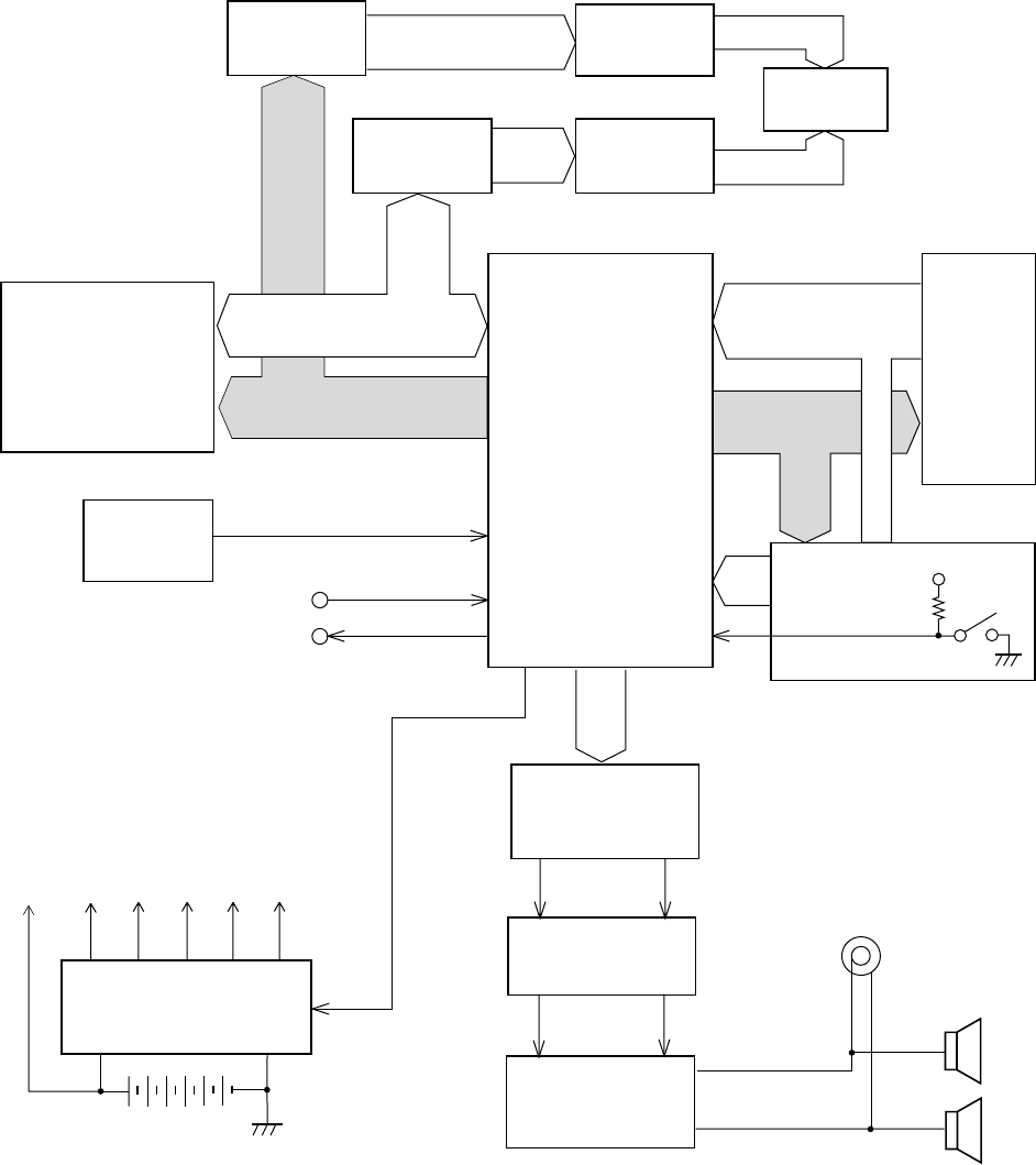
BLOCK DIAGRAM
KC0 ~ KC7
FI0 ~ FI7
SI0 ~ SI7
Sound Source ROM
(8M-bit)
LSI102
MX23C8100MC-
12CA19
LRCK, SO, BCK
D/A Converter
IC103
UPD6379GR
Filter
Q108, Q109
Power Amplifier
IC101
LA4598
LED driver
IC106
BA612
Keyboard
MA0 ~ MA19
Power Supply Circuit
Q101 ~ Q105, Q110, Q119
D104, D105, D109
VCC AVDD VDD
LVDD DVDD
VC
APO
MD0
~
MD7
Speakers
Output
MA8
~
MA11
LEDs /
7Seg. LED
LED driver
Q111 ~ Q118 La ~ Lg, Lp
MIDI IN
OUT
Buttons VDD
Power Switch
Reset IC
IC104
RE5VA35AA
RESET FI10
CPU
LSI101
UPD912GF-3BA
KI0
~ KI2
MD0 ~ MD15
LED Latch
IC105
HD74HC75P
LED Latch
IC107
HD74HC373P
NMI
— 4 —
Key
Second contact (2) First contact (1)
FI
KC
SI
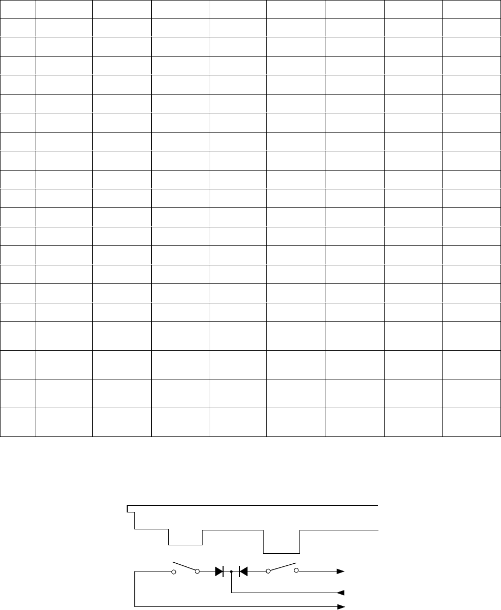
KC0 KC1 KC2 KC3 KC4 KC5 KC6 KC7
FI0 C2 (1) C#2 (1) D2 (1) D#2 (1) E2 (1) F2 (1) F#2 (1) G2 (1)
SI0 C2 (2) C#2 (2) D2 (2) D#2 (2) E2 (2) F2 (2) F#2 (2) G2 (2)
FI1 G#2 (1) A2 (1) A#2 (1) B2 (1) C3 (1) C#3 (1) D3 (1) D#3 (1)
SI1 G#2 (2) A2 (2) A#2 (2) B2 (2) C3 (2) C#3 (2) D3 (2) D#3 (2)
FI2 E3 (1) F3 (1) F#3 (1) G3 (1) G#3 (1) A3 (1) A#3 (1) B3 (1)
SI2 E3 (2) F3 (2) F#3 (2) G3 (2) G#3 (2) A3 (2) A#3 (2) B3 (2)
FI3 C4 (1) C#4 (1) D4 (1) D#4 (1) E4 (1) F4 (1) F#4 (1) G4 (1)
SI3 C4 (2) C#4 (2) D4 (2) D#4 (2) E4 (2) F4 (2) F#4 (2) G4 (2)
FI4 G#4 (1) A4 (1) A#4 (1) B4 (1) C5 (1) C#5 (1) D5 (1) D#5 (1)
SI4 G#4 (2) A4 (2) A#4 (2) B4 (2) C5 (2) C#5 (2) D5 (2) D#5 (2)
FI5 E5 (1) F5 (1) F#5 (1) G5 (1) G#5 (1) A5 (1) A#5 (1) B5 (1)
SI5 E5 (2) F5 (2) F#5 (2) G5 (2) G#5 (2) A5 (2) A#5 (2) B5 (2)
FI6 C6 (1) C#6 (1) D6 (1) D#6 (1) E6 (1) F6 (1) F#6 (1) G6 (1)
SI6 C6 (2) C#6 (2) D6 (2) D#6 (2) E6 (2) F6 (2) F#6 (2) G6 (2)
FI7 G#6 (1) A6 (1) A#6 (1) B6 (1) C7 (1)
SI7 G#6 (2) A6 (2) A#6 (2) B6 (2) C7 (2)
FI10 +-0
Accomp.
Volume Up
Main Vol.
Up Mode
KI0 Demo 3 2 1 Tempo
Up Main Vol.
Down Intro/
Fill-In
KI1
Transpose
Tune/MIDI
6 5 4 Rhythm
Accomp.
Vol. Down
Synchro/
Ending
KI2
Touch
Response
9 8 7 Tone Tempo
Down Start/
Stop
CIRCUIT DESCRIPTION
KEY MATRIX
Note: Each key has two contacts, the first conatct (1) and second contact (2).
— 5 —
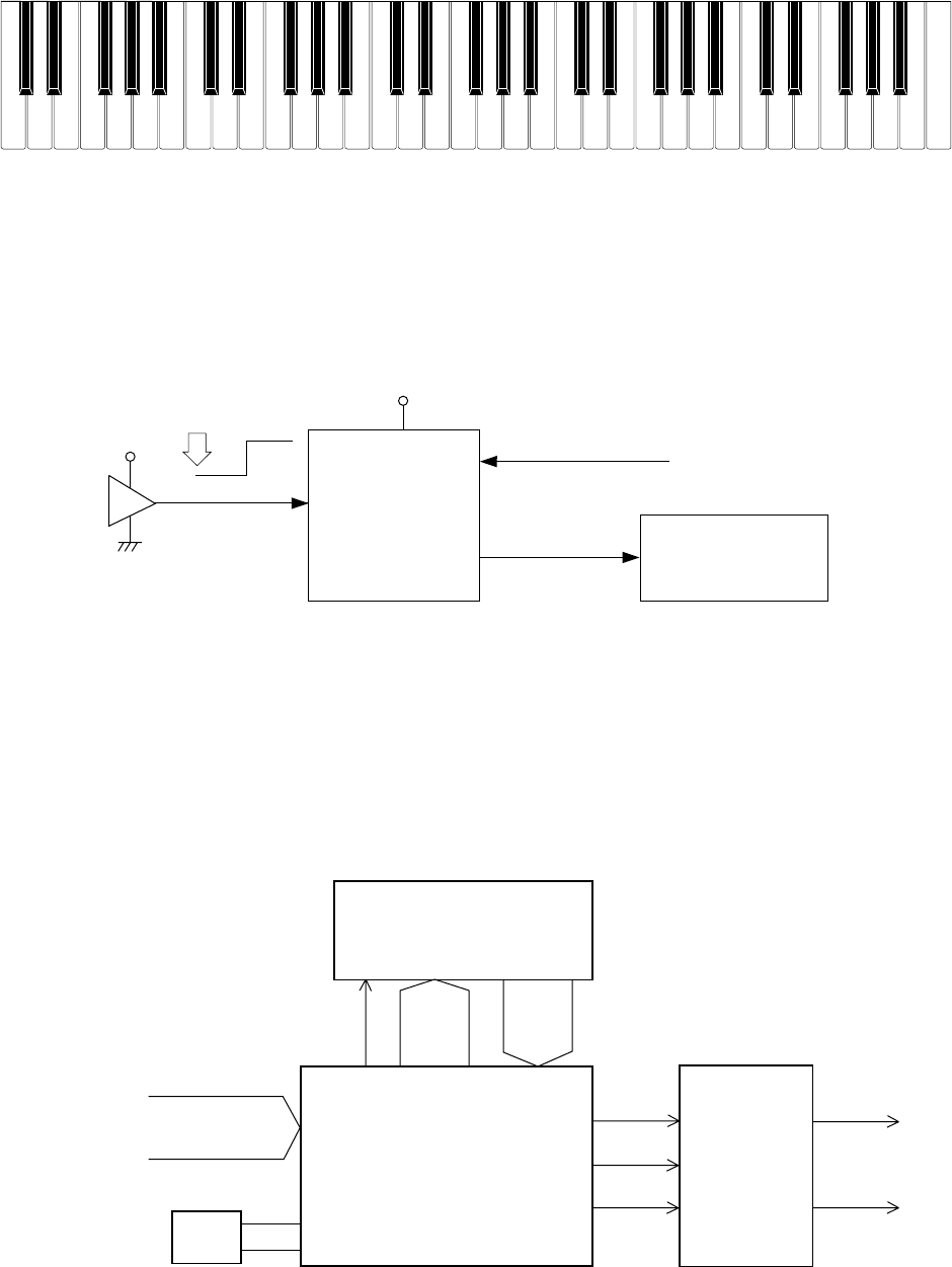
CPU
LSI101
UPD912GF-3BA
Sound Source ROM
LSI102
MX23C8100PC-12CA19
CE A0 ~ A18 D0 ~ D15
MA1 ~
MA19
MD0 ~
MD15
MSB0
FI0 ~ FI7
SI0 ~ SI7
SO
BOK
LRCK
PG
X101
20 MHz
DAC
IC103
UPD6379GR
LOUT
ROUT
SO: Sound data
BOK: Bit clock
LRCK: Word clock
SI
CLK
LRCK
From keyboard
Reset IC
IC104
RE5VA35AA Power Supply Circuit
VDD
Battery set
RESET
VDD
POWER From power switchNMI
APO
CPU
LSI101
UPD912GF-3BA
SCKO
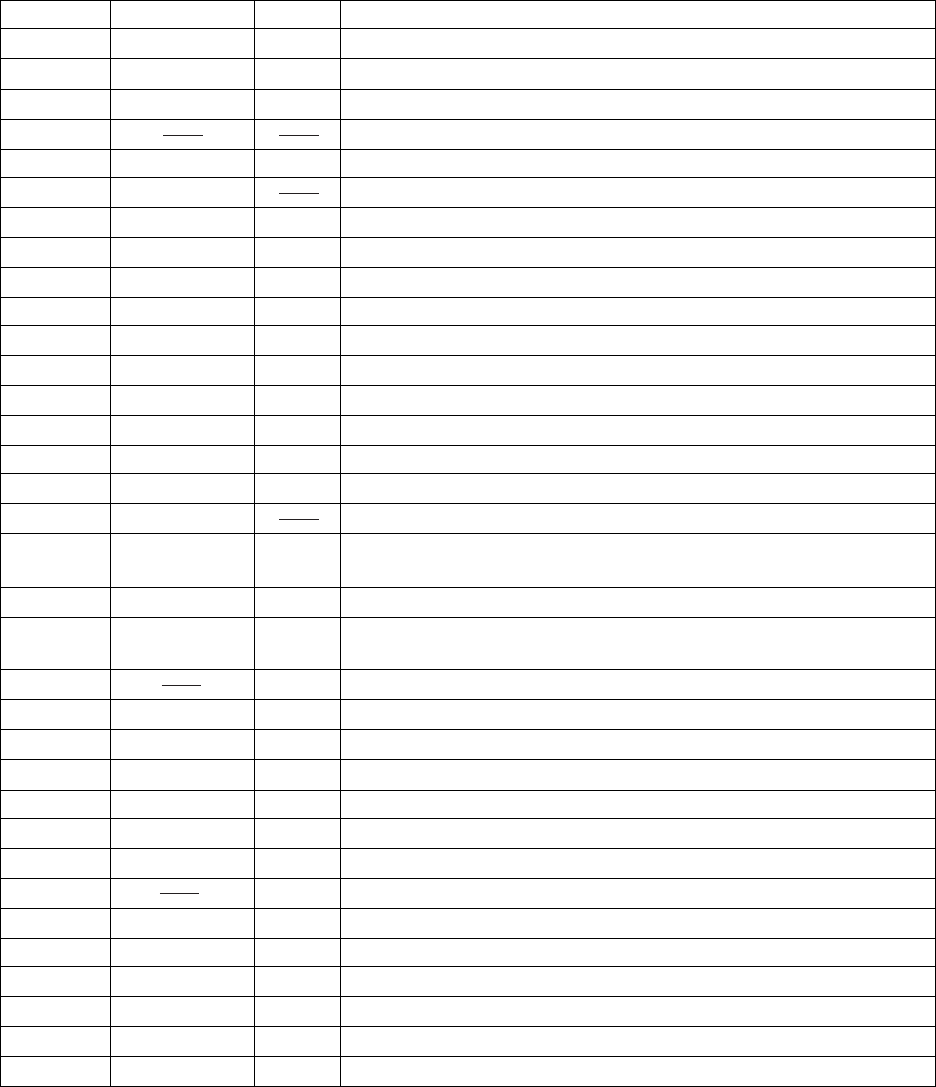
NOMENCLATURE OF KEYS
RESET CIRCUIT
When batteries are set or an AC adapter is connected, the reset IC provides a low pulse to the CPU. The CPU
then initializes its internal circuit.
When the power switch is pressed, the CPU receives a low pulse of POWER signal.The CPU raises APO signal
to +5 V to turn power on.
CPU (LSI101: UPD912GF-3BA)
The 16-bit CPU contains a 1k-byte RAM, three 8-bit I/O ports, two timers, a keycontroller and serial interfaces.
The CPU detects key velocity by counting the time between first-key input signal FI and second-key SI from
the keyboard. The CPU reads sound data and velocity data from the sound source ROM in accordance with
the selected tone; the CPU can read rhythm data simultaneously when a rhythm pattern is selected. Then the
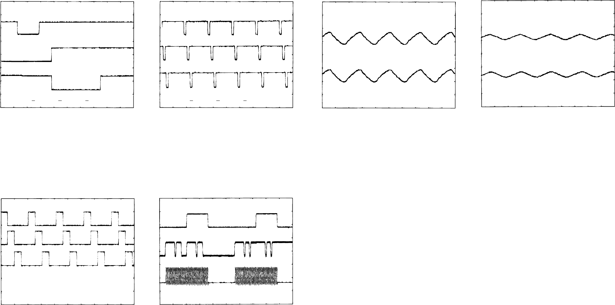
CPU provides 16-bit serial sound data to the DAC.The CPU also controls MIDI input/output and LED driving.
F#3 G#3 A#3 C#4 D#4 F#4 G#4 A#4 C#5 D#5 F#5 G#5 A#5
F3 G3 A3 B3 C4 D4 E4 F4 G4 A4 B4 C5 D5 E5 F5 G5 A5 B5 C6
D#3
C2 D2 E2 F2 G2 A2 B2 C3 D3 E3 B6A6G6F6E6D6 C7
C#3A#2G#2
F#2D#2
C#2 A#6
G#6F#6D#6
C#6
— 6 —
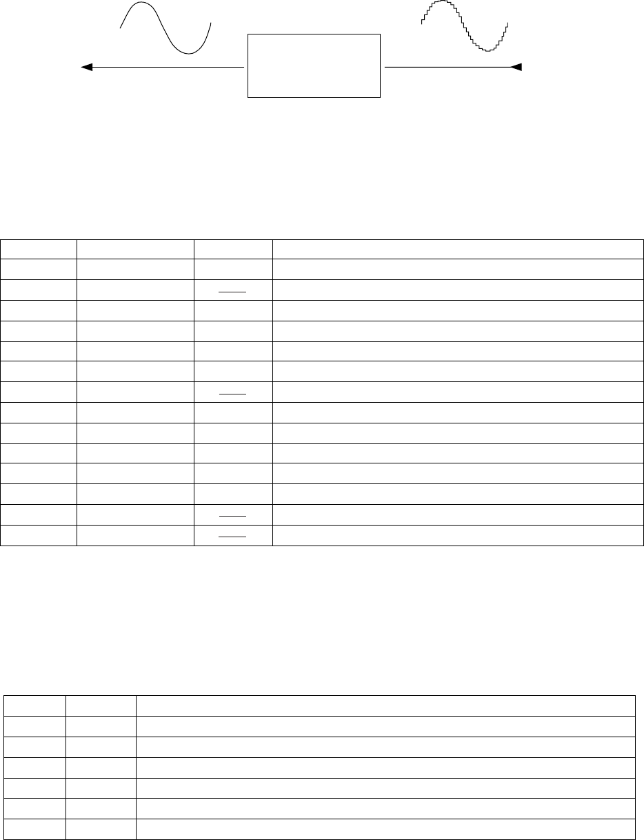
The following table shows the pin functions of LSI101.
DAC (IC103: UPD6379GR)
The DAC receives 16-bit serial data output from the CPU. The data contains digital sound data of the melody,
chord, bass, and percussion for the right and left channels. The DAC converts the data into analog waveforms
and output them to each channel separately.
Pin No. Terminal In/Out Function
1 TXD0 Out MIDI signal input
2 RXD0 In MIDI signal output
3 SCK0 Out APO (Auto Power Off) signal output
4 ~ 6 Not used. Connected to ground.
7 AVCC In Ground (0 V) source
8, 9 AN0, AN1 Not used. Connected to ground.
10 AGND In Ground (0 V) source
11 BCK Out Bit clock output
12 SO Out Serial sound data output
13 LRCK Out Word clock output
14 GND In Ground (0 V) source
15, 16 XLT0, XLT1 In/Out 20 MHz clock input/output
17 VCC In +5 V source
18, 19 MD0, MD1 In Mode selection terminal. Connected to ground.
20 RSTB In Reset signal input
21 NMI In Power ON signal input
22 INT Not used. Connected to ground.
23 ~ 30 FI0 ~ FI3
SI0 ~ SI3 In Key input signal
31 ~ 38 KC0 ~ KC7 Out Key scan signal output
39 ~ 46 FI4 ~ FI7
SI4 ~ SI7 In Key input signal
47 ~ 50 In Not used.
51 FI10 In Button input signal input
52 SI10 In Not used
53 ~ 55 KI0 ~ KI2 In Button input signal input
56 MWNB Out Not used.
57 ~ 76 MA1 ~ MA17 Out Address bus
77 MCSB0 Out Chip enable signal output for the sound source ROM
78, 79 Out Not used
80 VCC In +5 V source
81 GND In Ground (0 V) source
82 MRDB Out Read enable signal output for the sound source ROM
83 ~ 98 MD0 ~ MD15 In/Out Data bus
99 PLE Out Latch enable signal output for LED latches
100 P17 In APO cancellation signal input
— 7 —
Filter Block From DAC
To power amplifier
Name Voltage For operation of
VDD +5 V CPU, Reset IC, Sound source ROM, LED Latches
DVDD +5 V Power jack, Photocoupler
AVDD +5V DAC, Filter
LVDD +5 V LED Drivers
VCC +9 V Power amplifier, Pilot lamp
VC +9 V Power amplifier
Pin No. Terminal In/Out Function
1 Power GND In Ground (0V) source
2 Ch1 B.S. Terminal for a bootstrap capacitor
3 Ch1 OUT Out Channel 1 output
4 VCC In +9V source
5 Ch1 N.F. In Negative feedback input
6 Ch1 IN In Channel 1 input
7 D.C. Terminal for a decoupling capacitor
8 Pre GND In Ground (0V) source
9 Stand by In Power control signal input. 0 V: Off, +9 V: On
10 Ch2 IN In Channel 2 input
11 Ch2 N.F. In Negative feedback input
12 Ch2 OUT Out Channel 2 output
13 Ch2 B.S. Terminal for a bootstrap capacitor
14 NC Not used
POWER SUPPLY CIRCUIT
The power supply circuit generates six voltages as shown in the following table. VDD voltage is always
generated. The others are controlled by APO signal from the CPU.
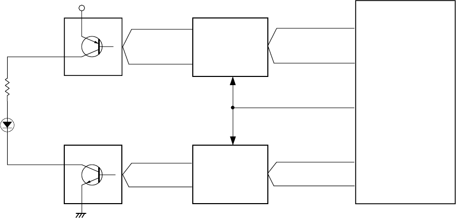
FILTER BLOCK
Since the sound signals from the DAC are stepped waveforms, the filter block is added to smooth the
waveforms.
POWER AMPLIFIER (IC102: LA4598)
The power amplifier is a two-channel amplifier with standby switch.
The following table shows the pin function of IC102.
— 8 —
LED Latch
IC107
HD74HC373AP
LG
CPU
LSI101
UPD912GF-3BA
LVDD
LED Latch
IC105
HD74HC75AP
PLE
IC106
BA612
LED Driver
LO0 ~LO3
Q111 ~Q118
LED Driver
MD0 ~ MD7
La ~ Lg, Lp
MD8 ~ MD11
LED DRIVING
— 9 —
1
2
3
CH1
CH2
CH3
4
5
6
A 5 ms
CH1
CH2
CH3
CH1: 5 V CH2: 5 V CH3: 5 V
–––
7
8
9
A 1 ms
CH1
CH2
CH1: 0.2 V CH2: 0.2 V
~~
C
D
E
F
A 1 ms
CH1
CH2
CH1: 0.2 V CH2: 0.2 V
~~
CH1
CH2
CH3
0
A
B
–––
CH1: 5 V CH2: 5 V CH3: 5 V
A 2 µs
0.1 s
CH1: CH2: 5 V5 V CH3: 5 V
50 µs
CH1
CH2
CH3
CH1: CH2: 5 V5 V CH3: 5 V
MAJOR WAVEFORMS
1POWER ON signal
UPD912GF-3BA pin 21
2APO signal
UPD912GF-3BA pin 3
3Reset signal for the DSP
UPD912G-3BA pin 99
4Key scan signal KC0
UPD912GF-3BA pin 31
5Key scan signal KC1
UPD912GF-3BA pin 32
6Key scan signal KC2
UPD912GF-3BA pin 33
CDAC output (R-ch)
UPD6379GR pin 5
DDAC output (L-ch)
UPD6379GR pin 8
EAmp. input (R-ch)
LA4598 pin 6
FAmp. input (L-ch)
LA4598 pin 10
7LED drive signal
BA612 pin 13
8LED drive signal
BA612 pin 12
9LED drive signal
BA612 pin 11
0Word clock LRCK
UPD912GF-3BA pin 13
AData signal SO
UPD912GF-3BA pin 12
BBit clock BCK
UPD912GF-3BA pin 11
Tone: Pan Flute (39)
Key: A4
Touch response: Off
Volume: Maximum
— 10 —
PCB VIEW AND CHECK POINTS
— 11 —
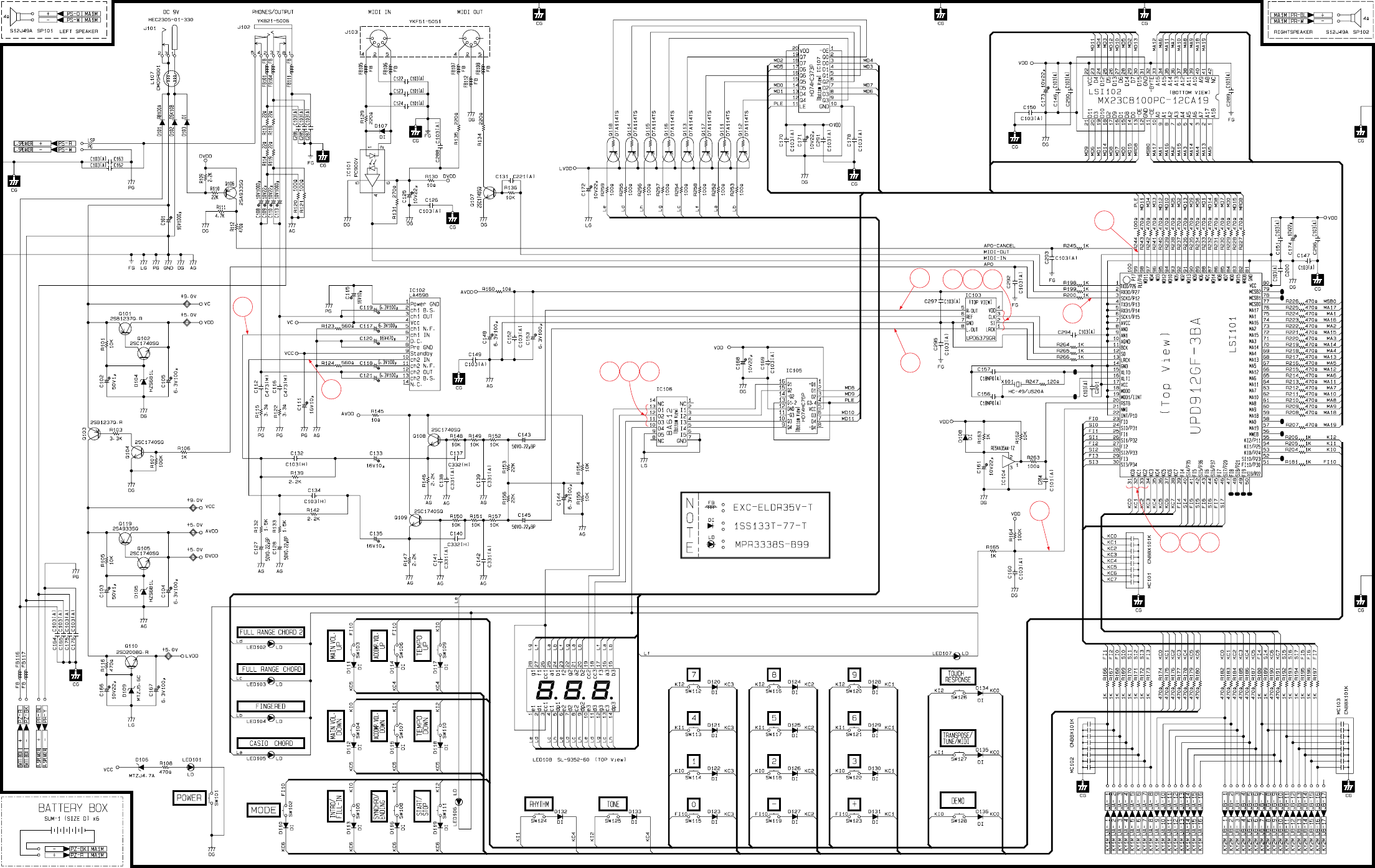
SCHEMATIC DIAGRAMS
JCM460-MA1M
15
16
5.1
4.5
5.1
8.3
7.6 5.7
5.1
0.7
0.0
8.2 7.5
5.1
5.1
5.7
7.5
5.1
5.7
0.0
5.1
2.3
1.7
1.7
2.3
7 8 9 14
13
2
3
4 5 6
1
10 11 12
— 12 —
JCM617T-KY1M/KY2M
20
11
10
9
7
6
5
4
3
1
2
9
12
13
14
15
16
17
18
19
17-1
17-2
22
21
23
8
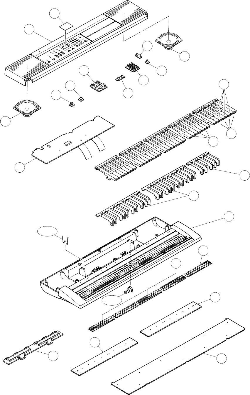
EXPLODED VIEW
— 13 —

Notes: 1. Prices and specifications are subject to change with-
out prior notice.
2. As for spare parts order and supply, refer to the
"GUIDEBOOK for Spare parts Supply", published
seperately.
3. The numbers in item column correspond to the same
numbers in drawing.
PARTS LIST
CTK-530
FOB Japan
N Item Code No. Parts Name Specification Q N.R.Yen R
Unit Price
Main PCB
N 8 6923 6930 PCB ass'y JCM460-MA1M M140198*1 1 5,550 B
N LSI101 2012 0168 LSI UPD912GF-3BA 1 750 A
N LSI102 2012 0686 LSI MX23C8100PC-12CA19 1 840 A
IC101 2114 1421 IC PC900V 1 210 B
IC102 2114 2891 IC LA4598 1 140 A
N IC103 2105 4249 LSI UPD6379GR 1 150 A
IC104 2105 3941 IC RE5VA35AA-TZ 1 44 A
N IC105 2105 4438 IC HD74HC75P 1 44 B
IC106 2114 3318 IC BA612 1 98 A
N IC107 2105 4431 IC HD74HC373P 1 85 B
Q101, Q103 2251 0469 Transistor 2SB1237Q,R-TV6-T 2 24 A
Q102, Q104, 2220 1387 Transistor 2SC1740SQ-TP-T 613 B
Q105,
Q107~Q109
Q106, Q119 2200 4409 Transistor 2SA933-SQ-TP-T 2 14 B
Q110 2253 0357 Transistor 2SD2008Q,R-T105-T 1 30 A
Q111~Q118 2259 1883 Digital transistor DTA114TS-TP-T 8 10 B
N X101 2590 2009 Cryatal oscillator HC-49/US20A 1 110 A
D101 2390 1316 Diode SB10-04A3-BT-T 1 28 B
D102 2390 0371 Diode DSK10B-BT-T 1 11 B
D103, D107, 2390 1344 Diode 1SS133T-77-T 30 3B
D108,
D110~D136
D104, D105 2360 1085 Zener diode HZS6B1LTD-T 2 10 A
D106 2360 2079 Zener diode MTZJ4.7AT-77-T 18A
D109 2360 1946 Zener diode MTZJ5.6CT-77-T 1 8 A
LED101~ 2370 1106 LED MPR3338S-B99 724 B
LED107
LED108 2370 1141 LED SL-9352-60 1 200 B
J101 3501 7049 Jack, Power HEC2305-01-330 1 29 A
J102 3612 0665 Jack, Phone YKB21-5006 1 60 B
J103 3501 4816 Jack, DIN YKF51-5051 1 110 B
L107 3841 1057 Coil CM05RB01 163 C
MC101~ 2845 0168 Module capacitor CNB8X101K 358 C
MC103
Keyboard PCBs
20 6923 6940 PCB ass'y M617T-KY1M M140211*1 1 750 B
D501~D564 2301 0101 Diode 1S2473-T-77-T 64 8 C
21 6923 6950 PCB ass'y M617T-KY2M M140212*1 1 710 B
D565~D622 2301 0101 Diode 1S2473-T-77-T 58 8 C
Mechanical Parts
N 1 6923 7050 Rubber button M340082-1 175 B
2 6922 2680 Rubber button M312082-2 1 29 B
N 3 6923 4331 Rubber button M312088A-2 197 B
N4 6923 7040 Rubber button M240127-1 1 95 B
N5 6923 7030 Rubber button M240096-1 1 160 B
N 6 6923 4990 Rubber button, MODE M312123-2 128 B
N 7 6923 4980 Rubber button, POWER M312122-2 128 B
N 9 3831 0833 Speaker S12J49A 2450 B
N 10 6923 7020 Panel M140046-1 11,300 B
N11 6923 7010 Display plate M340157-1 1 120 B
12 6922 2840 White key set, CEGB M111723-1 5 100 A
13 6922 2860 White key set, DFAS M111725-1 1100 A
Notes: N – New parts
M – Minimum order/supply quantity
R – Rank — 15 —
FOB Japan
N Item Code No. Parts Name Specification Q N.R.Yen R
Unit Price
14 6922 2850 White key set, DFA M111724-1 4100 A
15 6922 2750 Black key set, 5-key M111726-2 186 A
16 6922 2740 Black key set, 10-key M111726-1 2 120 A
N17 6923 7060 Case M140171*1 1 2,470 C
17-1 6902 6140 Battery spring (-) M41226-1 127B
17-2 6903 2150 Battery spring (+) M41330-1 118B
18 6922 2771 Key contact rubber M211704A-1 489A
19 6922 2761 Key contact rubber M211705A-1 191A
N22 6923 7000 Bottom plate M240116-1 1 630 C
23 6918 1636 Battery cover M311164F*1 1 200 B
Accessory
6916 7880 Music stand M310827-1 1 120 B
Notes: N – New parts
M – Minimum order/supply quantity
R – Rank
Description of Capacitors
A general description of capacitors is shown in the following table.
The description consists of Type, Value, Rated Voltage and Tolerance.
When you need a capacitor, please find a substitution in your country by yourselves referring to the
description.
Ref. No of Capacitor Description
C101, C107, C125, C211 Electrolytic, 16 V, 470 µF, +/-20%
C110, C153 Electrolytic, 6.3 V, 220 µF, +/-20%
C103, C104, C113, C114, C121, C137~C139, C145, C167, C171, C193,
C197 Electrolytic, 10 V, 22 µF, +/-20%
C108 Electrolytic, 16 V, 10 µF, +/-20%
C152, C162 Electrolytic, 50 V, 1 µF, +/-20%
C111, C182 Electrolytic, 6.3 V, 470 µF, +/-20%
C102, C124, C126, C134, C159~C161 Electrolytic, 6.3 V, 100 µF, +/-20%
C123, C127 Electrolytic, 10 V, 100 µF, +/-20%
C144, C165 Semiconductive, 16 V, 2200 pF, +/-10%
C147, C164 Semiconductive, 16 V, 0.033 µF, +/-10%
C130, C131 Semiconductive, 16 V, 0.047 µF, +/-10%
C128, C129, C154, C174 Semiconductive, 16 V, 0.01 µF, +/-10%
C118, C119 Semiconductive, 16 V, 0.018 µF, +/-10%
C140, C155, C166, C170, C175~C179, C181, C185, C186, C188, C189,
C192, C194~C196, C198, C200 Ceramic, 50 V, 0.1 µF, +80/-20%
C105, C120, C132, C133, C135, C136, C141, C142, C146~C150, C163,
C172, C173, C180, C184, C187, C212~C214 Ceramic, 50 V, 100 pF, +/-10%
C122, C199 Ceramic, 50 V, 1000 pF, +/-10%
C168 Ceramic, 50 V, 0.01 µF, +/-20%
C191 Semiconductive, 16 V, 33 pF, +/-10%
C156, C157 Semiconductive, 16 V, 4 pF, +/-0.5 pF
C190 Semiconductive, 16 V, 22 pF, +/-10%
C116, C117 Mylar, 50 V, 0.047 µF, +/-10%
C112, C115 Electrolytic, 10 V, 1000 µF, +/-20%
— 16 —

Description of Resistors
A general description of resistors is shown in the following table.
The description consists of Type, Value, Rated Wattage and Tolerance.
When you need a resistor, please find a substitution in your country by yourselves referring to the
description.
Note:
All resistors are carbon film, 1/5 watt, +/-5% otherwise specified.
Ref. No of Resistor Description
R107, R137, R145~R147, R150, R163, R164, R168~R170, R189 1 KΩ
R102, R103, R133, R135, R142 220 Ω
R220~R230 330 Ω
R132, R143, R159, R185, R292 10 Ω
R115, R116, R127, R139~R141, R149, R158, R166, R171~R173,
R186~R188, R206, R208~R211, R213, R215 100 Ω
R175, R212, R214 100 KΩ
R105, R138, R148, R161, R274, R293, R295 10 KΩ
R110, R291 22 Ω
R117, R118 3.3 Ω
R111~R114 82 Ω
R125, R126, R160 4.7 KΩ
R207 1.5 KΩ
R134 2.2 KΩ
R136 270 Ω
R106, R108, R151~R157, R165, R251~R273, R275~R283 470 Ω
R104, R294 47 KΩ
R178~R184, R218, R219, R231~R250 56 KΩ
R216 1 MΩ
R174, R176, R177, R192~R199 33 KΩ
R123, R124, R130, R131 15 KΩ
R128, R129 5.6 KΩ
R217 560 Ω
R162, R167 18 KΩ
R190, R191, R200~R205 33 Ω
R120, R121, R144 47 Ω
— 17 —
MA0700951A