Chongqing Jinou Science and Technology Development BLE0305C2P Bluetooth Low Energy Module (BLE) User Manual BLE0305C2P
Chongqing Jinou Science & Technology Development Co., Ltd. Bluetooth Low Energy Module (BLE) BLE0305C2P
UserManual.wiki
>
Chongqing Jinou Science and Technology Development
>
BLE0305C2P User Manual
user manual
Navigation menu
Upload a User Manual
Namespaces
Wiki Guide
HTML
PDF
Info
Views
User Manual
Discussion / Help
Navigation
![ChongQing JINOU Science & Technology BLE0305C2P Bluetooth Module Data Sheet http://www.jinoux.com +86-23-68798999 Page 2 of 18 4. Pin Descriptions Device Terminal Functions(设备接线端列表) 序号 说明 说明 序号1 GND GND 38 2 P25 P24 37 3 P26 P23 36 4 P27 P22 35 5 P28 SWD 34 6 P29 SWC 33 7 P30 P21 32 8 P31 P20 31 9 P02 P19 30 10 P03 P18 29 11 P04 P17 28 12 P05 P16 27 13 VCC P15 26 14 GND P14 25 15 16 17 18 19 20 21 22 23 24 GND VCC P06 P07 P08 P09 P10 P11 P12 P13 Device Terminal Functions(设备接线端功能描述) No. Name Type Description P00 XL1 Digital I/O Analog input General purpose I/O Connection for 32.768 kHz crystal (LFXO) P01 XL2 Digital I/O Analog input General purpose I/O Connection for 32.768 kHz crystal (LFXO) P02 AIN0 Digital I/O Analog input General purpose I/O SAADC/COMP/LPCOMP input P03 AIN1 Digital I/O Analog input General purpose I/O SAADC/COMP/LPCOMP input P04 AIN2 Digital I/O Analog input General purpose I/O SAADC/COMP/LPCOMP input P05 AIN3 Digital I/O Analog input General purpose I/O SAADC/COMP/LPCOMP input P06 Digital I/O General purpose I/O P07 Digital I/O General purpose I/O P08 Digital I/O General purpose I/O NFC1 P09 NFC input Digital I/O NFC antenna connection General purpose I/O**1 NFC2 P10 NFC input Digital I/O NFC antenna connection General purpose I/O**1 P11 Digital I/O General purpose I/O P12 Digital I/O General purpose I/O P13 Digital I/O General purpose I/O P14 TRACEDATA[3] Digital I/O General purpose I/O Trace port output P15 TRACEDATA[2] Digital I/O General purpose I/O Trace port output P16 TRACEDATA[1] Digital I/O General purpose I/O Trace port output P17 Digital I/O General purpose I/O P18 TRACEDATA[0] / SWO Digital I/O General purpose I/O Trace port output / Single wire output P19 Digital I/O General purpose I/O P20 Digital I/O General purpose I/O](https://usermanual.wiki/Chongqing-Jinou-Science-and-Technology-Development/BLE0305C2P/User-Guide-3979435-Page-3.png)
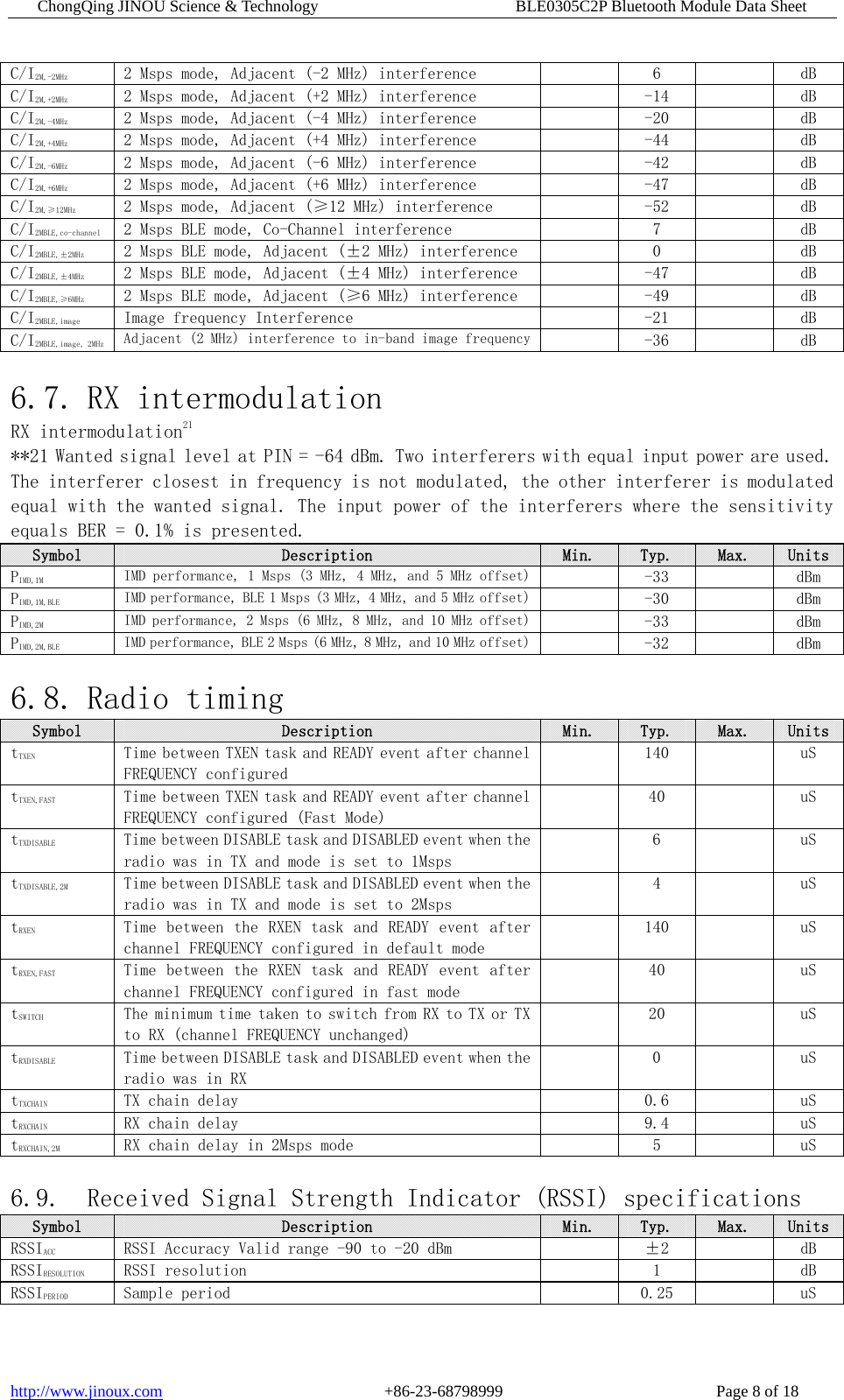
![ChongQing JINOU Science & Technology BLE0305C2P Bluetooth Module Data Sheet http://www.jinoux.com +86-23-68798999 Page 7 of 18 6.4. Transmitter specification Symbol Description Min. Typ. Max. UnitsPRF Maximum output power 4 6 dBm PRFC RF power control range 24 dB PRFCR RF power accuracy ±4 dB PRF1,1 1st Adjacent Channel Transmit Power 1 MHz (1 Msps Nordic proprietary mode) -25 dBc PRF2,1 2nd Adjacent Channel Transmit Power 2 MHz (1 Msps Nordic proprietary mode) -50 dBc PRF1,2 1st Adjacent Channel Transmit Power 2 MHz (2 Msps Nordic proprietary mode) -25 dBc PRF2,2 2nd Adjacent Channel Transmit Power 4 MHz (2 Msps Nordic proprietary mode) -50 dBc PRF1,2,BLE 1st Adjacent Channel Transmit Power 2 MHz (2 Msps BLE mode) -20 dBc PRF2,2,BLE 2nd Adjacent Channel Transmit Power 4 MHz (2 Msps BLE mode) -50 dBc 6.5. Receiver operation Symbol Description Min. Typ. Max. UnitsPRX,MAX Maximum received signal strength at < 0.1% BER 0 dBm PSENS,IT,1M Sensitivity, 1Msps nRF mode 16 -93 dBm PSENS,IT,SP,1M,BLE Sensitivity, 1Msps BLE ideal transmitter, <=37 bytes BER=1E-3 17 -96 dBm PSENS,IT,LP,1M,BLE Sensitivity, 1Msps BLE ideal transmitter >=128 bytes BER=1E-4 18 -95 dBm PSENS,IT,2M Sensitivity, 2Msps nRF mode 19 -89 dBm PSENS,IT,SP,2M,BLE Sensitivity, 2Msps BLE ideal transmitter, Packet length <=37bytes -93 dBm PSENS,DT,SP,2M,BLE Sensitivity, 2Msps BLE dirty transmitter, Packet length <=37bytes -93 dBm PSENS,IT,LP,2M,BLE Sensitivity, 2Msps BLE ideal transmitter >= 128bytes -92 dBm PSENS,DT,LP,2M,BLE Sensitivity, 2Msps BLE dirty transmitter, Packet length >= 128bytes -92 dBm **16 Typical sensitivity applies when ADDR0 is used for receiver address correlation. When ADDR[1...7] are used for receiver address correlation, the typical sensitivity for this mode is degraded by 3dB. **17 As defined in the Bluetooth Core Specification v4.0 Volume 6: Core System Package (Low Energy Controller Volume) **18 Equivalent BER limit < 10E-04 **19 Typical sensitivity applies when ADDR0 is used for receiver address correlation. When ADDR[1...7] are used for receiver address correlation, the typical sensitivity for this mode is degraded by 3dB. 6.6. selectivity RX selectivity with equal modulation on interfering signal20 **20 Wanted signal level at PIN = -67 dBm. One interferer is used, having equal modulation as the wanted signal. The input power of the interferer where the sensitivity equals BER = 0.1% is presented Symbol Description Min. Typ. Max. UnitsC/I1M,co-channel 1Msps mode, Co-Channel interference 9 dB C/I1M,-1MHz 1 Msps mode, Adjacent (-1 MHz) interference -2 dBC/I1M,+1MHz 1 Msps mode, Adjacent (+1 MHz) interference -10 dBC/I1M,-2MHz 1 Msps mode, Adjacent (-2 MHz) interference -19 dBC/I1M,+2MHz 1 Msps mode, Adjacent (+2 MHz) interference -42 dBC/I1M,-3MHz 1 Msps mode, Adjacent (-3 MHz) interference -38 dBC/I1M,+3MHz 1 Msps mode, Adjacent (+3 MHz) interference -48 dBC/I1M,±6MHz 1 Msps mode, Adjacent (≥6 MHz) interference -50 dBC/I1MBLE,co-channel 1 Msps BLE mode, Co-Channel interference 6 dBC/I1MBLE,-1MHz 1 Msps BLE mode, Adjacent (-1 MHz) interference -2 dBC/I1MBLE,+1MHz 1 Msps BLE mode, Adjacent (+1 MHz) interference -9 dBC/I1MBLE,-2MHz 1 Msps BLE mode, Adjacent (-2 MHz) interference -22 dBC/I1MBLE,+2MHz 1 Msps BLE mode, Adjacent (+2 MHz) interference -46 dBC/I1MBLE,>3MHz 1 Msps BLE mode, Adjacent (≥3 MHz) interference -50 dBC/I1MBLE,image Image frequency Interference -22 dBC/I1MBLE,image,1MHz Adjacent (1 MHz) interference to in-band image frequency -35 dBC/I2M,co-channel 2Msps mode, Co-Channel interference 10 dB](https://usermanual.wiki/Chongqing-Jinou-Science-and-Technology-Development/BLE0305C2P/User-Guide-3979435-Page-8.png)
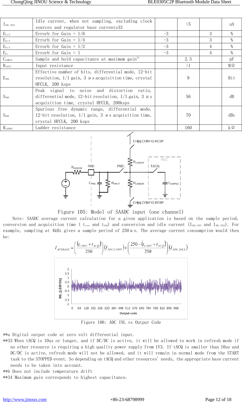
![ChongQing JINOU Science & Technology BLE0305C2P Bluetooth Module Data Sheet http://www.jinoux.com +86-23-68798999 Page 10 of 18 8. SAADC - Successive approximation analog-todigital converter 8.1. Reference The ADC can use two different references, controlled in the REFSEL field of the CH[n].CONFIG register. These are: • Internal reference • VCC as reference The internal reference results in an input range of ±0.6 V on the ADC core. VCC as reference results in an input range of ±VCC/4 on the ADC core. The gain block can be used to change the effective input range of the ADC. Input range = (+/- 0.6 V or +/-VDD/4)/Gain For example, choosing VCC as reference, single ended input (grounded negative input), and a gain of 1/4 the input range will be: Input range = (VCC/4)/(1/4) = VCC With internal reference, single ended input (grounded negative input), and a gain of 1/6 the input range will be: Input range = (0.6 V)/(1/6) = 3.6 V The AIN0-AIN7 inputs cannot exceed VCC, or be lower than GND. 8.2. Acquisition time To sample the input voltage, the ADC connects a capacitor to the input. For illustration, see Figure 103: Simplified ADC sample network on page. The acquisition time indicates how long the capacitor is connected, see TACQ field in CH[n].CONFIG register. The required acquisition time depends on the source (Rsource) resistance. For high source resistance the acquisition time should be increased, see Table 89: Acquisition time on page. Figure 103: Simplified ADC sample network Table 89: Acquisition time TACQ [μs] Maximum source resistance [kOhm] 3 10 5 40 10 100 15 200 20 400 40 800 8.3. Limits event monitoring A channel can be event monitored by configuring limit register CH[n].LIMIT. If the conversion result is higher than the defined high limit, or lower than the defined low limit, the appropriate event will get fired.](https://usermanual.wiki/Chongqing-Jinou-Science-and-Technology-Development/BLE0305C2P/User-Guide-3979435-Page-11.png)
![ChongQing JINOU Science & Technology BLE0305C2P Bluetooth Module Data Sheet http://www.jinoux.com +86-23-68798999 Page 11 of 18 Figure 104: Example of limits monitoring on channel 'n' Note that when setting the limits, CH[n].LIMIT.HIGH shall always be higher than or equal to CH[n].LIMIT.LOW . In other words, an event can be fired only when the input signal has been sampled outside of the defined limits. It is not possible to fire an event when the input signal is inside a defined range by swapping high and low limits. The comparison to limits always takes place, there is no need to enable it. If comparison is not required on a channel, the software shall simply ignore the related events. In that situation, the value of the limits registers is irrelevant, so it does not matter if CH[n].LIMIT.LOW is lower than CH[n].LIMIT.HIGH or not. 8.4. SAADC Electrical Specification Symbol Description Min. Typ. Max. UnitsDNL Differential non-linearity, 10-bit resolution -0.95 <1 LSB INL Integral non-linearity, 10-bit resolution 1 LSB VOS Differential offset error (calibrated), 10-bit resolutiona ±2 LSB CEG Gain error temperature coefficient 0.02 % / ℃fSAMPLE Maximum sampling rate 200 kHz tACQ,10k Acquisition time (configurable), source Resistance <= 10kOhm 3 uS tACQ,40k Acquisition time (configurable), source Resistance <= 40kOhm 5 uS tACQ,100k Acquisition time (configurable), source Resistance <= 100kOhm 10 uS tACQ,200k Acquisition time (configurable), source Resistance <= 200kOhm 15 uS tACQ,400k Acquisition time (configurable), source Resistance <= 400kOhm 20 uS tACQ,800k Acquisition time (configurable), source Resistance <= 800kOhm 40 uS tCONV Conversion time <2 uS IADC,CONV ADC current during ACQuisition and CONVersion 700 uA](https://usermanual.wiki/Chongqing-Jinou-Science-and-Technology-Development/BLE0305C2P/User-Guide-3979435-Page-12.png)