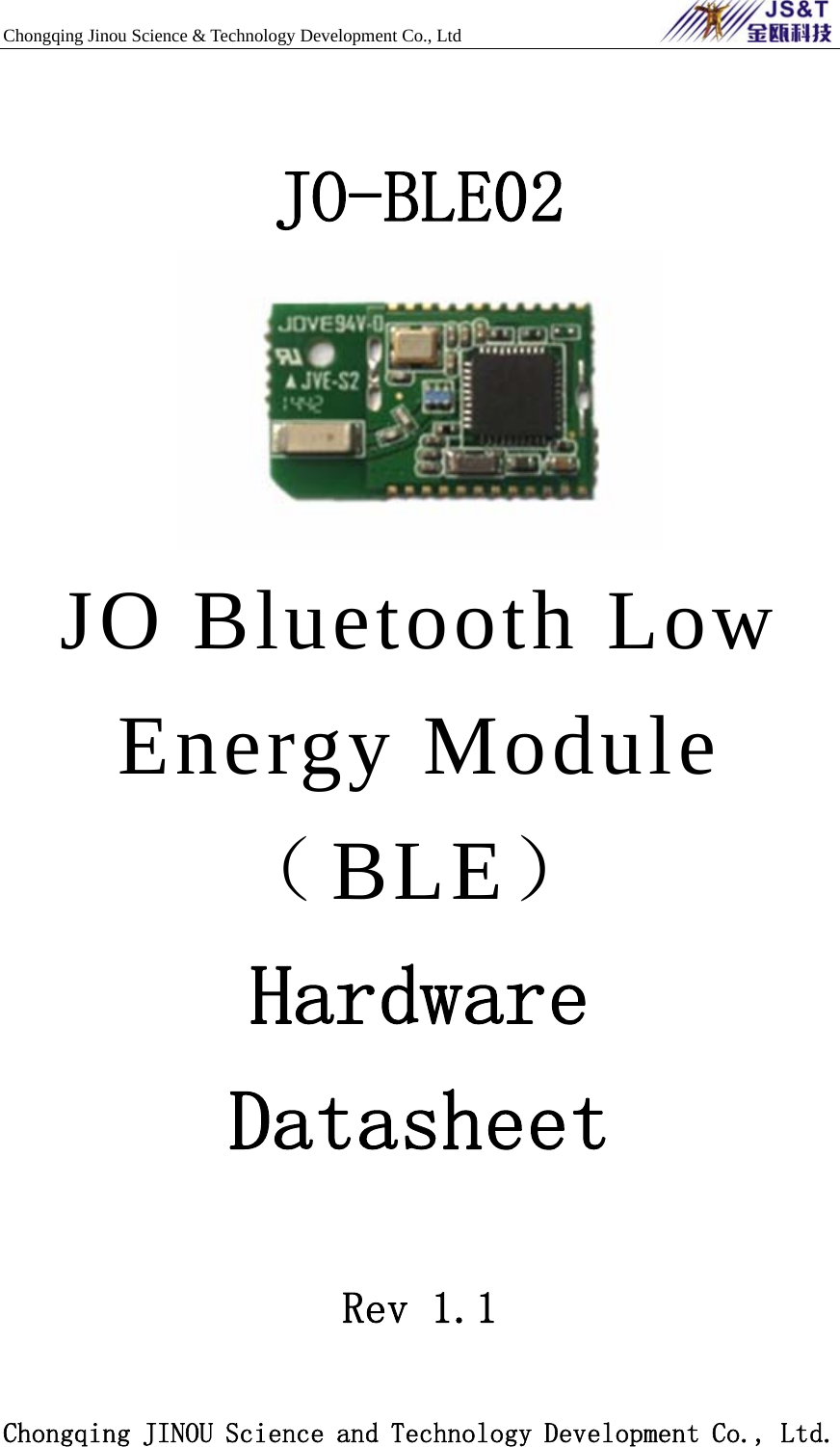
Chongqing Jinou Science and Technology Development
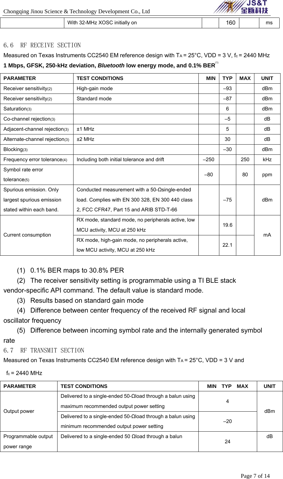
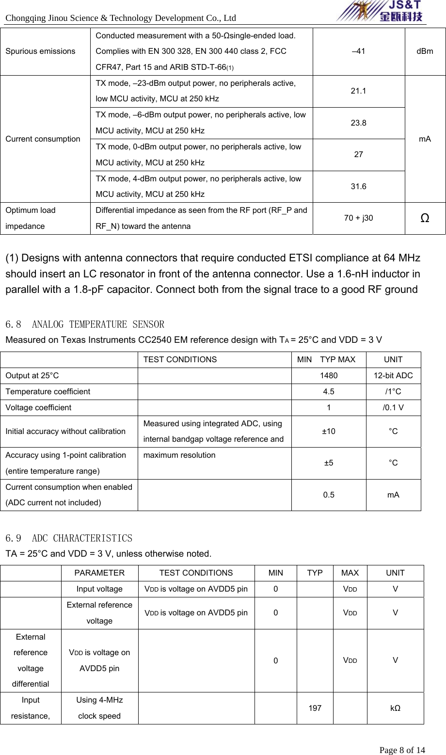
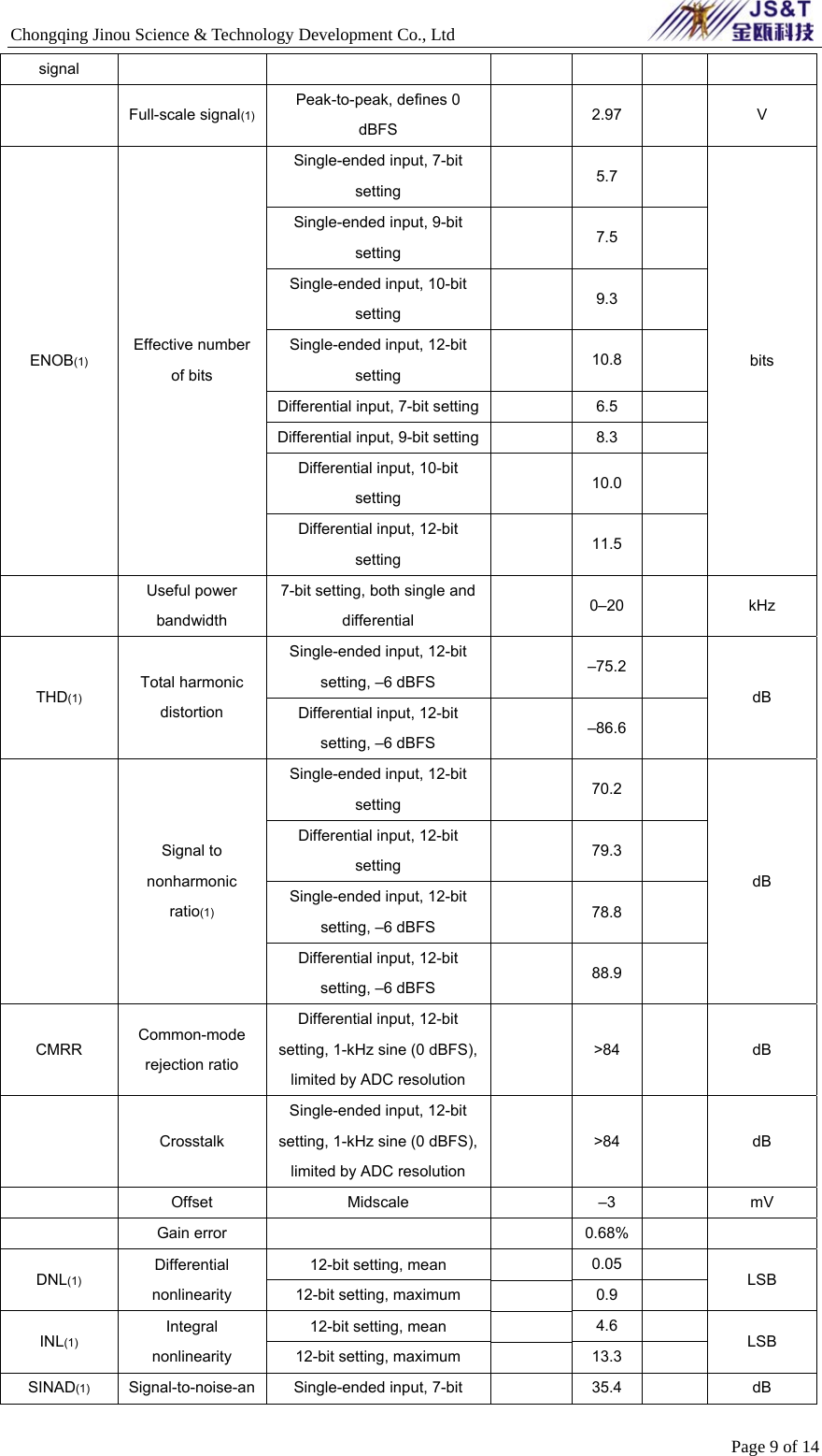
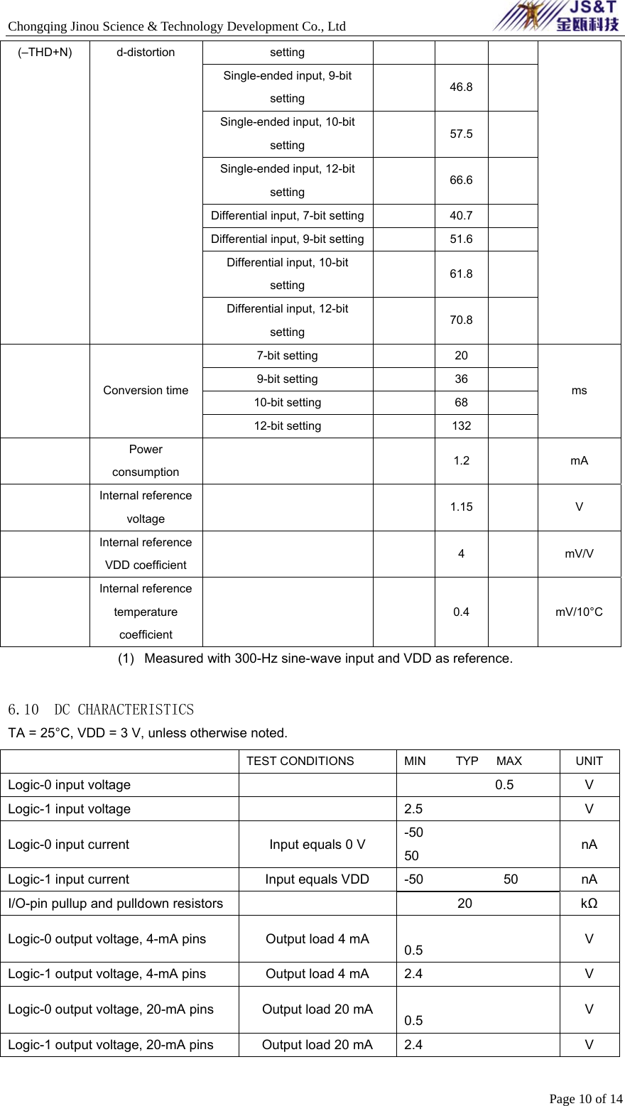
 JO-BLE02 JO Bluetooth Low Energy Module (BLE) User Manual manual

Chongqing JINOU Science and Technology Development JO Bluetooth Low Energy Module (BLE) manual

Users Manual

Chongqing Jinou Science & Technology Development Co., Ltd                          JO-BLE02  JO Bluetooth Low Energy Module(BLE) Hardware Datasheet  Rev 1.1   Chongqing JINOU Science and Technology Development Co., Ltd.
Chongqing Jinou Science & Technology Development Co., Ltd                        Page 1 of 1 Contents 1. Features ............................................................................................................................... 2 2. Product Description ......................................................................................................... 3 3. Applications .......................................................................................................................... 3 4. Block Diagram ...................................................................................................................... 4 5. Pin Descriptions ............................................................................................................... 4 5.1  Device Terminal ........................................................................................................... 4 5.2  Device Terminal Functions ....................................................................................... 4 6. Electrical Specifications ........................................................................................................ 5 6.1  ABSOLUTE MAXIMUM RATINGS ......................................................................................... 5 6.2  RECOMMENDED OPERATING CONDITIONS ......................................................................... 6 6.3  ELECTRICAL CHARACTERISTICS ..................................................................................... 6 6.4  GENERAL CHARACTERISTICS ........................................................................................... 6 6.6  RF RECEIVE SECTION ..................................................................................................... 7 6.7  RF TRANSMIT SECTION ................................................................................................... 7 6.8  ANALOG TEMPERATURE SENSOR ....................................................................................... 8 6.9  ADC CHARACTERISTICS ................................................................................................... 8 6.10  DC CHARACTERISTICS ................................................................................................. 10 7. BLOCK DESCRIPTION .................................................................................................... 11 8. Solder Profiles ..................................................................................................................... 13 9. Physical Dimensions ........................................................................................................... 14
Chongqing Jinou Science & Technology Development Co., Ltd                        Page 1 of 14 Document History Revision  Date  Change Reason 1.0  2012-05-25 Original publication of this document. 1.1  2014-11-07  Updates include: increase the length of module.
Chongqing Jinou Science & Technology Development Co., Ltd                        Page 2 of 14  JO-BLE02    1. Features  · True Single-Chip BLE Solution: CC2540 Can Run Both Application and BLE Protocol Stack,              Includes Peripherals to Interface With Wide Range of Sensors ,Etc. · Programmable Output Power Up to 4.5 dBm   · IR Generation Circuitry · Powerful Five-Channel DMA · 12-Bit ADC With Eight Channels and Configurable Resolution  · Two Powerful USARTs With Support for Several Serial Protocols  · 19 General-Purpose I/O Pins   · Low Power Mode:  Active Mode RX Down to 19.6 mA  Active Mode TX (-6dBm):24 mA  Power Mode 1 (3-ms Wake-Up): 235 uA    Power Mode 2 (Sleep Timer On): 0.9 uA   Power Mode 3 (External Interrupts): 0.4 uA  · Wide Supply-Voltage Range (2 V–3.6 V)  Full RAM and Register Retention in All Power Modes · Nominal Supply Voltage at 3.3±0.1V · Surface-mount, Size: 24.1×14.5 (unit:mm  error = ±0.2mm)
Chongqing Jinou Science & Technology Development Co., Ltd                        Page 3 of 14 2. Product Description  The JO-BLE02 module (chip CC2540) is a cost-effective, low-power, true system-on-chip (SoC) for Bluetooth low energy applications. It enables robust  BLE  master  or  slave  nodes  to  be  built  with  very  low  total bill-of-material costs. The CC2540 combines an excellent RF transceiver with an industry-standard enhanced 8051 MCU, in-system programmable flash memory,  8-KB  RAM,  and  many  other  powerful  supporting  features  and peripherals. The CC2540 is suitable for systems where very low power consumption is required. Very low-power sleep modes are available. Short transition  times  between  operating  modes  further  enable  low  power consumption.  The CC2540 comes in two different versions: CC2540F128/F256, with 128 and 256 KB of flash memory, respectively.  Combined with the Bluetooth low energy protocol stack from Texas Instruments, the CC2540F128/F256 forms the market’s most flexible and cost-effective single-mode Bluetooth low energy solution.  3. Applications   2.4-GHz Bluetooth low energy Systems   Mobile Phone Accessories  Sports and Leisure Equipment  Consumer Electronics   Human Interface Devices(Keyboard,Mouse,Remote Control)  USB Dongles  Health Care and Medical
Chongqing Jinou Science & Technology Development Co., Ltd                        Page 4 of 14 4. Block Diagram   5. Pin Descriptions  5.1  Device Terminal No.  Des    Des  No. 1  P2_0  A0 | P0_0  24 2  P2_2 | DC  P0_1  23 3  P2_1 | DD  RX | P0_2  22 4  P1_7  TX | P0_3  21 5  P1_6  CT | P0_4  20 6  P1_3  RT | P0_5  19 7  P1_4  RST  18 8  P1_5  P0_6  17 9  USB_N  P0_7  16 10  USB_P  P1_0  15 11  VCC  P1_1  14 12  GND  P1_2  13  5.2  Device Terminal Functions PIN  NAME  PIN   TYPE   DESCRIPTION 1  P2_0  Digital I/O  Port 2.0  2  P2_2 | DC  Digital I/O  Port 2.2  Debug Clock  Debug data interface 3  P2_1 | DD  Digital I/O  Port 2.1  Debug Data  Debug data interface 4  P1_7  Digital I/O  Port 1.7 5  P1_6  Digital I/O  Port 1.6
Chongqing Jinou Science & Technology Development Co., Ltd                        Page 5 of 14 6  P1_3  Digital I/O  Port 1.3 7  P1_4  Digital I/O  Port 1.4 8  P1_5  Digital I/O  Port 1.5 9  USB_N  Digital I/O  USB N 10  USB_P  Digital I/O  USB P 11  Vcc  Power Supply  +3.3V Power Supply 12  GND  Ground  Connect to GND 13  P1-2  Digital I/O  Port 1.2  14  P1-1  Digital I/O  Port 1.1 20-mA drive capability 15  P1-0  Digital I/O  Port 1.0 20-mA drive capability 16  P0-7  Digital I/O  Port 0.7  17  P0-6  Digital I/O  Port 0.6 18  RST  Digital input  Reset, active-low 19  RT | P0_5  Digital O  UART request to send active low Digital I/O  Port 0.5 20  CT | P0_4  Digital I  UART clear to send active low Digital I/O  Port 0.4 21  TX | P0_3  Digital O  UART data output Digital I/O  Port 0.3 22  RX | P0_2  Digital I  UART data input Digital I/O  Port 0.2 23  P0_1  Digital I/O  Port 0.1 24  A0 | P0_0  Analog I  ADC  Digital I/O  Port 0.0     6. Electrical Specifications 6.1  ABSOLUTE MAXIMUM RATINGS    MIN MAX UNIT Supply voltage    All supply pins must have the same voltage    –0.3  3.9  V Voltage on any digital pin   –0.3 VDD + 0.3, ≤ 3.9 V Input RF level    10 dBm Storage temperature range   –40 125  °C ESD(2)  All pads, according to human-body model, JEDEC STD 22, method A114     2 kV According to charged-device model, JEDEC STD 22, method C101     500 V (1) Stresses beyond those listed under Absolute Maximum Ratings may cause permanent damage to the
Chongqing Jinou Science & Technology Development Co., Ltd                        Page 6 of 14 device. These are stress ratings only, and functional operation of the device at these or any other conditions beyond those indicated under Recommended Operating Conditions is not implied. Exposure to absolute-maximum-rated conditions for extended periods may affect device reliability.   (2) CAUTION: ESD-sensitive device. Precautions should be used when handling the device in order to prevent permanent damage.   6.2  RECOMMENDED OPERATING CONDITIONS   MIN MAX UNIT Operating ambient temperature range, TA   –40  125   °C  Operating supply voltage   2  3.6   V   6.3  ELECTRICAL CHARACTERISTICS  Measured on Texas Instruments CC2540 EM reference design with TA = 25°C and VDD = 3 V     PARAMETER  TEST CONDITIONS   MIN   TYP   MAX   UNIT lcore Core current consumption Power mode 1. Digital regulator on; 16-MHz RCOSC and 32-MHz crystal oscillator off; 32.768-kHz XOSC, POR, BOD and sleep timer active; RAM and register retention 235   uA  Power mode 2. Digital regulator off; 16-MHz RCOSC and 32-MHz crystal oscillator off; 32.768-kHz XOSC, POR, and sleep timer active; RAM and register retention    0.9    Power mode 3. Digital regulator off; no clocks; POR active; RAM and register retention  0.4    Low MCU activity: 32-MHz XOSC running. No radio or peripherals. No flash access, no RAM access.  6.7     mA    Iperi Peripheral Current Consumption (Adds to core current Icore for each peripheral unit activated)   Timer 1  Timer running, 32-MHz XOSC used     90    mA Timer 2  Timer running, 32-MHz XOSC used     90    mA Timer 3  Timer running, 32-MHz XOSC used     60    mA Timer 4  Timer running, 32-MHz XOSC used     70    mA Sleep timer Including 32.753-kHz RCOSC     0.6    mA ADC When converting    1.2    mA  6.4  GENERAL CHARACTERISTICS  Measured on Texas Instruments CC2540 EM reference design with TA = 25°C and VDD = 3 V    TEST CONDITIONS MIN   TYP   MAX   UNIT WAKE-UP AND TIMING     Power mode 1 → active Digital regulator on, 16-MHz RCOSC and 32-MHz crystal oscillator off. Start-up of 16-MHz RCOSC   4    ms Power mode 2 or 3 → active  Digital regulator off, 16-MHz RCOSC and 32-MHz crystal oscillator off. Start-up of regulator and 16-MHz RCOSC   120    ms Active → TX or RX   Crystal ESR = 16 Ω. Initially running on 16-MHz RCOSC, with 32-MHz XOSC OFF 410    ms
Chongqing Jinou Science & Technology Development Co., Ltd                        Page 7 of 14 With 32-MHz XOSC initially on     160   ms  6.6  RF RECEIVE SECTION  Measured on Texas Instruments CC2540 EM reference design with TA = 25°C, VDD = 3 V, fc = 2440 MHz   1 Mbps, GFSK, 250-kHz deviation, Bluetooth low energy mode, and 0.1% BER(1)  PARAMETER   TEST CONDITIONS   MIN   TYP   MAX UNIT Receiver sensitivity(2)   High-gain mode     –93   dBm Receiver sensitivity(2)   Standard mode     –87   dBm Saturation(3)     6   dBm Co-channel rejection(3)     –5   dB  Adjacent-channel rejection(3)   ±1 MHz     5   dB  Alternate-channel rejection(3)   ±2 MHz     30   dB  Blocking(3)     –30   dBm Frequency error tolerance(4)   Including both initial tolerance and drift    –250   250  kHz   Symbol rate error tolerance(5)   –80  80 ppm Spurious emission. Only largest spurious emission stated within each band.   Conducted measurement with a 50-Ωsingle-ended load. Complies with EN 300 328, EN 300 440 class 2, FCC CFR47, Part 15 and ARIB STD-T-66    –75   dBm Current consumption   RX mode, standard mode, no peripherals active, low MCU activity, MCU at 250 kHz     19.6  mA  RX mode, high-gain mode, no peripherals active, low MCU activity, MCU at 250 kHz     22.1     (1)  0.1% BER maps to 30.8% PER     (2)  The receiver sensitivity setting is programmable using a TI BLE stack vendor-specific API command. The default value is standard mode.     (3)  Results based on standard gain mode     (4)  Difference between center frequency of the received RF signal and local oscillator frequency     (5)  Difference between incoming symbol rate and the internally generated symbol rate  6.7  RF TRANSMIT SECTION  Measured on Texas Instruments CC2540 EM reference design with TA = 25°C, VDD = 3 V and  fc = 2440 MHz   PARAMETER   TEST CONDITIONS   MIN  TYP  MAX  UNIT Output power   Delivered to a single-ended 50-Ωload through a balun using maximum recommended output power setting   4 dBm Delivered to a single-ended 50-Ωload through a balun using minimum recommended output power setting   –20 Programmable output power range   Delivered to a single-ended 50 Ωload through a balun   24 dB
Chongqing Jinou Science & Technology Development Co., Ltd                        Page 8 of 14 Spurious emissions   Conducted measurement with a 50-Ωsingle-ended load. Complies with EN 300 328, EN 300 440 class 2, FCC CFR47, Part 15 and ARIB STD-T-66(1)  –41 dBm  TX mode, –23-dBm output power, no peripherals active, low MCU activity, MCU at 250 kHz   21.1 mA Current consumption   TX mode, –6-dBm output power, no peripherals active, low MCU activity, MCU at 250 kHz   23.8 TX mode, 0-dBm output power, no peripherals active, low MCU activity, MCU at 250 kHz   27  TX mode, 4-dBm output power, no peripherals active, low MCU activity, MCU at 250 kHz   31.6 Optimum load impedance  Differential impedance as seen from the RF port (RF_P and RF_N) toward the antenna   70 + j30  Ω   (1) Designs with antenna connectors that require conducted ETSI compliance at 64 MHz should insert an LC resonator in front of the antenna connector. Use a 1.6-nH inductor in parallel with a 1.8-pF capacitor. Connect both from the signal trace to a good RF ground  6.8  ANALOG TEMPERATURE SENSOR  Measured on Texas Instruments CC2540 EM reference design with TA = 25°C and VDD = 3 V    TEST CONDITIONS MIN  TYP MAX UNIT  Output at 25°C     1480 12-bit ADC Temperature coefficient     4.5 /1°C  Voltage coefficient     1 /0.1 V  Initial accuracy without calibration   Measured using integrated ADC, using internal bandgap voltage reference and ±10 °C  Accuracy using 1-point calibration (entire temperature range)   maximum resolution   ±5 °C  Current consumption when enabled (ADC current not included)    0.5 mA   6.9  ADC CHARACTERISTICS  TA = 25°C and VDD = 3 V, unless otherwise noted.    PARAMETER TEST CONDITIONS MIN TYP MAX UNIT  Input voltage  VDD is voltage on AVDD5 pin 0   VDD  V  External reference voltage VDD is voltage on AVDD5 pin 0   VDD  V External reference voltage differential VDD is voltage on AVDD5 pin  0  VDD  V Input resistance, Using 4-MHz clock speed   197   kΩ
Chongqing Jinou Science & Technology Development Co., Ltd                        Page 9 of 14 signal  Full-scale signal(1) Peak-to-peak, defines 0 dBFS   2.97   V ENOB(1) Effective number of bits Single-ended input, 7-bit setting   5.7   bits Single-ended input, 9-bit setting   7.5   Single-ended input, 10-bit setting   9.3   Single-ended input, 12-bit setting   10.8   Differential input, 7-bit setting  6.5   Differential input, 9-bit setting  8.3   Differential input, 10-bit setting   10.0   Differential input, 12-bit setting   11.5    Useful power bandwidth 7-bit setting, both single and differential   0–20  kHz THD(1) Total harmonic distortion Single-ended input, 12-bit setting, –6 dBFS   –75.2  dB Differential input, 12-bit setting, –6 dBFS   –86.6   Signal to nonharmonic ratio(1) Single-ended input, 12-bit setting   70.2   dB Differential input, 12-bit setting   79.3   Single-ended input, 12-bit setting, –6 dBFS   78.8   Differential input, 12-bit setting, –6 dBFS   88.9   CMRR Common-mode rejection ratio Differential input, 12-bit setting, 1-kHz sine (0 dBFS), limited by ADC resolution  >84   dB  Crosstalk Single-ended input, 12-bit setting, 1-kHz sine (0 dBFS), limited by ADC resolution  >84   dB  Offset Midscale  –3   mV  Gain error    0.68%   DNL(1) Differential nonlinearity 12-bit setting, mean   0.05   LSB 12-bit setting, maximum   0.9   INL(1) Integral nonlinearity 12-bit setting, mean   4.6   LSB 12-bit setting, maximum   13.3   SINAD(1)  Signal-to-noise-an Single-ended input, 7-bit   35.4   dB
Chongqing Jinou Science & Technology Development Co., Ltd                        Page 10 of 14 (–THD+N) d-distortion  setting Single-ended input, 9-bit setting   46.8   Single-ended input, 10-bit setting   57.5   Single-ended input, 12-bit setting   66.6   Differential input, 7-bit setting  40.7   Differential input, 9-bit setting  51.6   Differential input, 10-bit setting   61.8   Differential input, 12-bit setting   70.8    Conversion time 7-bit setting   20   ms 9-bit setting   36   10-bit setting   68   12-bit setting   132    Power consumption    1.2   mA  Internal reference voltage    1.15   V  Internal reference VDD coefficient    4   mV/V  Internal reference temperature coefficient   0.4   mV/10°C (1)  Measured with 300-Hz sine-wave input and VDD as reference.    6.10  DC CHARACTERISTICS  TA = 25°C, VDD = 3 V, unless otherwise noted.    TEST CONDITIONS MIN     TYP   MAX  UNIT Logic-0 input voltage               0.5  V  Logic-1 input voltage      2.5  V   Logic-0 input current    Input equals 0 V  -50              50  nA  Logic-1 input current   Input equals VDD  -50            50  nA  I/O-pin pullup and pulldown resistors             20  kΩ  Logic-0 output voltage, 4-mA pins    Output load 4 mA                  0.5  V  Logic-1 output voltage, 4-mA pins    Output load 4 mA  2.4  V   Logic-0 output voltage, 20-mA pins    Output load 20 mA                  0.5  V  Logic-1 output voltage, 20-mA pins    Output load 20 mA  2.4  V
Chongqing Jinou Science & Technology Development Co., Ltd                        Page 11 of 14  7. BLOCK DESCRIPTION CPU and Memory   The  8051 CPU core is a single-cycle 8051-compatible core. It has three different memory access busses (SFR, DATA, and CODE/XDATA), a debug interface, and an 18-input extended interrupt unit.   The memory arbiter is at the heart of the system, as it connects the CPU and DMA controller with the physical memories and all peripherals through the SFR bus. The memory arbiter has four memory-access points, access of which can map to one of three physical memories: an SRAM, flash memory, and XREG/SFR registers. It is responsible for performing arbitration and sequencing between simultaneous memory accesses to the same physical memory.   The SFR bus is drawn conceptually in Figure 8 as a common bus that connects all hardware peripherals to the memory arbiter. The SFR bus in the block diagram also provides access to the radio registers in the radio register bank, even though these are indeed mapped into XDATA memory space.   The  8-KB SRAM maps to the DATA memory space and to parts of the XDATA memory spaces. The SRAM is an ultralow-power SRAM that retains its contents even when the digital part is powered off (power modes 2 and 3).   The 128/256 KB flash block provides in-circuit programmable non-volatile program memory for the device, and maps into the CODE and XDATA memory spaces.   Peripherals   Writing to the flash block is performed through a flash controller that allows page-wise erasure and 4-bytewise programming. See User Guide for details on the flash controller.   A versatile five-channel DMA controller is available in the system, accesses memory using the XDATA memory space, and thus has access to all physical memories. Each channel (trigger, priority, transfer mode, addressing mode, source and destination pointers, and transfer count) is configured with DMA descriptors that can be located anywhere in memory. Many of the hardware peripherals (AES core, flash controller, USARTs, timers, ADC interface, etc.) can be used with the DMA controller for efficient operation by performing data transfers between a single SFR or XREG address and flash/SRAM.   Each CC2540 contains a unique 48-bit IEEE address that can be used as the public device address for a Bluetooth device. Designers are free to use this address, or provide their own, as described in the Bluetooth specfication.  The  interrupt controller services a total of 18 interrupt sources, divided into six interrupt groups, each of which is associated with one of four interrupt priorities. I/O and sleep timer interrupt requests are serviced even if the device is in a sleep mode (power modes 1 and 2) by bringing the CC2540 back to the active mode.   The  debug interface implements a proprietary two-wire serial interface that is used for in-circuit debugging. Through this debug interface, it is possible to erase or program the entire flash memory, control which oscillators are enabled, stop and start execution of the user program, execute instructions on the 8051 core, set code breakpoints, and single-step through
Chongqing Jinou Science & Technology Development Co., Ltd                        Page 12 of 14 instructions in the code. Using these techniques, it is possible to perform in-circuit debugging and external flash programming elegantly.   The  I/O controller is responsible for all general-purpose I/O pins. The CPU can configure whether peripheral modules control certain pins or whether they are under software control, and if so, whether each pin is configured as an input or output and if a pullup or pulldown resistor in the pad is connected. Each peripheral that connects to the I/O pins can choose between two different I/O pin locations to ensure flexibility in various applications.   The sleep timer is an ultralow-power timer that can either use an external 32.768-kHz crystal oscillator or an internal 32.753-kHz RC oscillator. The sleep timer runs continuously in all operating modes except power mode   3. Typical applications of this timer are as a real-time counter or as a wake-up timer to get out of power modes 1 or 2.   A built-in watchdog timer allows the CC2540 to reset itself if the firmware hangs. When enabled by software, the watchdog timer must be cleared periodically; otherwise, it resets the device when it times out. Timer 1 is a 16-bit timer with timer/counter/PWM functionality. It has a programmable prescaler, a 16-bit period value, and five individually programmable counter/capture channels, each with a 16-bit compare value. Each of the counter/capture channels can be used as a PWM output or to capture the timing of edges on input signals. It can also be configured in IR generation mode, where it counts timer 3 periods and the output is ANDed with the output of timer 3 to generate modulated consumer IR signals with minimal CPU interaction.   Timer 2 is a 40-bit timer used by the Bluetooth low energy stack. It has a 16-bit counter with a configurable timer period and a 24-bit overflow counter that can be used to keep track of the number of periods that have transpired. A 40-bit capture register is also used to record the exact time at which a start-of-frame delimiter is received/transmitted or the exact time at which transmission ends. There are two 16-bit timer-compare registers and two 24-bit overflow-compare registers that can be used to give exact timing for start of RX or TX to the radio or general interrupts.   Timer 3 and timer 4 are 8-bit timers with timer/counter/PWM functionality. They have a programmable prescaler, an 8-bit period value, and one programmable counter channel with an 8-bit compare value. Each of the counter channels can be used as PWM output.   USART 0 and USART 1 are each configurable as either an SPI master/slave or a UART. They provide double buffering on both RX and TX and hardware flow control and are thus well suited to high-throughput full-duplex applications. Each USART has its own high-precision baud-rate generator, thus leaving the ordinary timers free for other uses. When configured as SPI slaves, the USARTs sample the input signal using SCK directly instead of using some oversampling scheme, and are thus well-suited for high data rates.   The AES encryption/decryption core allows the user to encrypt and decrypt data using the AES algorithm with 128-bit keys. The AES core also supports ECB, CBC, CFB, OFB, CTR, and CBC-MAC, as well as hardware support for CCM.   The ADC supports 7 to 12 bits of resolution with a corresponding range of bandwidths from 30-kHz to 4-kHz, respectively. DC and audio conversions with up to eight input channels (I/O
Chongqing Jinou Science & Technology Development Co., Ltd                        Page 13 of 14 controller pins) are possible. The inputs can be selected as single-ended or differential. The reference voltage can be internal, AVDD, or a single-ended or differential external signal. The ADC also has a temperature-sensor input channel. The ADC can automate the process of periodic sampling or conversion over a sequence of channels.   The operational amplifier is intended to provide front-end buffering and gain for the ADC. Both inputs as well as the output are available on pins, so the feedback network is fully customizable. A chopper-stabilized mode is available for applications that need good accuracy with high gain.   The ultralow-power analog comparator enables applications to wake up from PM2 or PM3 based on an analog signal. Both inputs are brought out to pins; the reference voltage must be provided externally. The comparator output is connected to the I/O controller interrupt detector and can be treated by the MCU as a regular I/O pin interrupt 8. Solder Profiles Composition of the solder ball:  Sn 95.5%, Ag 4.0%, Cu 0.5%  Typical Lead-Free Re-flow Solder Profile  Key features of the profile:   Initial Ramp = 1-2.5°C/sec to 175°C±25°C equilibrium   Equilibrium time = 60 to 180 seconds   Ramp to Maximum temperature (250°C) = 3°C/sec max.   Time above liquidus temperature (217°C):  45-90 seconds   Device absolute maximum reflow temperature: 260°C  Devices will withstand the specified profile. Lead-free devices will withstand up to three reflows to a maximum temperature of 260°C. Notes:They need to be baked prior to mounting。
Chongqing Jinou Science & Technology Development Co., Ltd                        Page 14 of 14 9. Physical Dimensions    A  B  C  D  E  F  G   1.525  1.27  0.89  14.48  24.13  2.44  1.91  mm 60  50  35  570  950  96  75  mil error:±0.2mm   Recommend PCB Layout
Chongqing Jinou Science & Technology Development Co., Ltd                        Page 15 of 14   A  B  C   0.81  0.51  0.76  mm 32  20  30  mil error:±0.1mm  FCC ID statement  This equipment complies with Part 15 of the FCC Rules.  Operation is subject to the following two conditions:  (1) This device may not cause harmful interference, and  (2) This device must accept any interference received, including interference that may cause undesired operation.   Any changes or modifications not expressly approved by the party responsible for compliance could void the user's authority to operate this equipment  IC ID statement  This device complies with industry Canada's licence-exempt RSSs.Operation is subject to the following two conditions:  (1) This device may not cause interference, and  (2) This device must accept any interference, including interference that may cause undesired operation of the device.   Le présent appareil est conforme aux CNR d'Industrie Canada applicables aux appareils radio exempts de licence. L'exploitation est autorisée aux deux conditions suivantes:  (1) l'appareil ne doit pas produire de brouillage, et  (2) l'utilisateur de l'appareil doit accepter tout brouillage radioélectrique subi, même si le  brouillage est susceptible d'en compromettre le fonctionnement.
Chongqing Jinou Science & Technology Development Co., Ltd                        Page 16 of 14  RF exposure warning  This  equipment  must  be  installed  and  operated  in  accordance  with  provide instructions and the antenna used for this transmitter must be installed to provide a separation distance of at least 20 cm from all persons and must not be co-located or operation in conjunction with any other antenna or transmitter. End-users and installers must be provide with antenna installation instructions and transmitter operating conditions for satisfying RF exposure compliance.   Information for the OEMs and Integrators  The following statement must be included with all versions of this document supplied to an OEM or integrator, but should not be distributed to the end user.  This device is intended for OEM integrators only.  Please see the full grant of equipment document for other restrictions.  Information to be supplied to the end user by the OEM or Integrator  The following regulator and safety notices must be published in documentation supplied to the end user of the product or system incorporating an adapter in compliance with local regulation. Host system must be labeled as following:  “Contains transmitter module FCC ID: SI8JO-BLE02, IC ID: 12627A-JOBLE02”      Chongqing Jinou Science & Technology Development Co., Ltd Address: 12-2-1-1, Huaxuan Branch Road 108#, Yuzhou Road, Jiulongpqo District, Chongqing, 400041, China, Tel: 86-23-68903066/68842136 Fax: 86-23-68644164 Web: www.oemblue.com    www.jinoux.com    E-mail: info@oemblue.com   Lauren@oemblue.com  jinou_lisa@foxmail.com

Navigation menu