CipherLab 8300W WLAN Module User Manual KCJ 1 Spec V1 1 0423
CipherLab Co., Ltd. WLAN Module KCJ 1 Spec V1 1 0423
UserManual.wiki
>
CipherLab
>
8300W User Manual
Users Manual
Navigation menu
Upload a User Manual
Namespaces
Wiki Guide
HTML
PDF
Info
Views
User Manual
Discussion / Help
Navigation
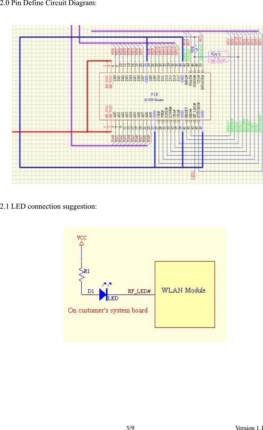
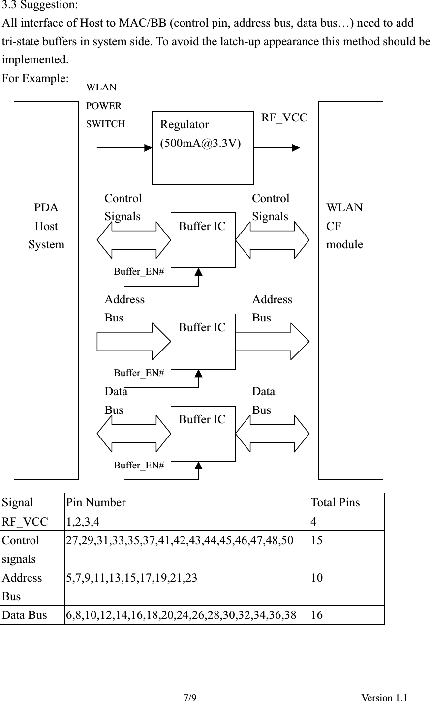
![6/9 Version 1.1 ඔ碁ઝݾैٝڶૻֆNo. 10-1 , Li-hsin Road I Science-based Industrial Park , Hsinchu 300,Taiwan, R.O.C.Tel: 886-3-6667799 Fax: 886-3-6667711Web site: www.wneweb.com 3.0 Timing Specification: 3.1 Power On Reset Configuration: Power on reset was issued from Host to the ISL3871IK18 MAC/BB through the RESET pin or via the soft reset bit. The Host system applies RESET at least [1ms after VCC has reached 90% of its end value] and the hold time is at least 1ms. (see PC-Card standard, Vol.2, CH.4.12.1). Please see ISL3871IK18 MAC/BB datasheet page 20 for the detail. 3.2 WLAN module initial procedure: 48 CD1# 41 RESET 42 IREQ# Interface signal1,2,3,4, RF_VCC >1ms >20ms Rising time between 0.1ms to 300msRESET at least 1ms after VCC has reached 90% of its value If WLAN is not ready in 20ms WLAN module is ready System Buffer_EN#](https://usermanual.wiki/CipherLab/8300W/User-Guide-719751-Page-6.png)