CipherLab 8300W WLAN Module User Manual KCJ 1 Spec V1 1 0423
CipherLab Co., Ltd. WLAN Module KCJ 1 Spec V1 1 0423
Users Manual

1/9 Version 1.1
802.11b CF WLAN Module
User's Guide
(Version 1.0)

2/9 Version 1.1
ඔ碁ઝݾैٝڶૻֆ
No. 10-1 , Li-hsin Road I
Science-based Industrial Park ,
Hsinchu 300,Taiwan, R.O.C.
Tel: 886-3-6667799
Fax: 886-3-6667711
Web site: www.wneweb.com
1.0 Pin Define:
Pin
Number
Pin Name Pin I/O Type Description
1RF_VCC Power, 0.3A DC Power Supply 3.3V ̈́5%
2RF_VCC Power, 0.3A DC Power Supply 3.3V ̈́5%
3RF_VCC Power, 0.3A DC Power Supply 3.3V ̈́5%
4RF_VCC Power, 0.3A DC Power Supply 3.3V ̈́5%
5A00 5V tol, BiDir, 2mA, 50K Pull Down Host PC Card Address Input, Bits 0
6D00 5V tol, BiDir, 2mA, 50K Pull Down Host PC Card Data Bus, Bits 0
7A01 5V tol, BiDir, 2mA, 50K Pull Down Host PC Card Address Input, Bits 1
8D01 5V tol, BiDir, 2mA, 50K Pull Down Host PC Card Data Bus, Bits 1
9A02 5V tol, BiDir, 2mA, 50K Pull Down Host PC Card Address Input, Bits 2
10 D02 5V tol, BiDir, 2mA, 50K Pull Down Host PC Card Data Bus, Bits 2
11 A03 5V tol, BiDir, 2mA, 50K Pull Down Host PC Card Address Input, Bits 3
12 D03 5V tol, BiDir, 2mA, 50K Pull Down Host PC Card Data Bus, Bits 3
13 A04 5V tol, BiDir, 2mA, 50K Pull Down Host PC Card Address Input, Bits 4
14 D04 5V tol, BiDir, 2mA, 50K Pull Down Host PC Card Data Bus, Bits 4
15 A05 5V tol, BiDir, 2mA, 50K Pull Down Host PC Card Address Input, Bits 5
16 D05 5V tol, BiDir, 2mA, 50K Pull Down Host PC Card Data Bus, Bits 5
17 A06 5V tol, BiDir, 2mA, 50K Pull Down Host PC Card Address Input, Bits 6
18 D06 5V tol, BiDir, 2mA, 50K Pull Down Host PC Card Data Bus, Bits 6
19 A07 5V tol, BiDir, 2mA, 50K Pull Down Host PC Card Address Input, Bits 7
20 D07 5V tol, BiDir, 2mA, 50K Pull Down Host PC Card Data Bus, Bits 7
21 A08 5V tol, BiDir, 2mA, 50K Pull Down Host PC Card Address Input, Bits 8
22 GND Ground Digital Ground
23 A09 5V tol, BiDir, 2mA, 50K Pull Down Host PC Card Address Input, Bits 9
24 D08 5V tol, BiDir, 2mA, 50K Pull Down Host PC Card Data Bus, Bits 8
25 GND Ground Digital Ground
26 D09 5V tol, BiDir, 2mA, 50K Pull Down Host PC Card Data Bus, Bits 9
27 OE# 5V tol, BiDir, 2mA, 50K Pull Up Host PC Card Memory Attribute Space
Output Enable
28 D10 5V tol, BiDir, 2mA, 50K Pull Down Host PC Card Data Bus, Bits 10
29 WE# 5V tol, COMS, Input, 50K Pull Up Host PC Card Memory Attribute Space
Write Enable

3/9 Version 1.1
ඔ碁ઝݾैٝڶૻֆ
No. 10-1 , Li-hsin Road I
Science-based Industrial Park ,
Hsinchu 300,Taiwan, R.O.C.
Tel: 886-3-6667799
Fax: 886-3-6667711
Web site: www.wneweb.com
30 D11 5V tol, BiDir, 2mA, 50K Pull Down Host PC Card Data Bus, Bits 11
31 IORD# 5V tol, BiDir, 2mA, 50K Pull Up Host PC Card I/O Space Read Strobe
32 D12 5V tol, BiDir, 2mA, 50K Pull Down Host PC Card Data Bus, Bits 12
33 IOWR# 5V tol, BiDir, 2mA, 50K Pull Up Host PC Card Space I/O Write Strobe
34 D13 5V tol, BiDir, 2mA, 50K Pull Down Host PC Card Data Bus, Bits 13
35 CE1# 5V tol, BiDir, 2mA, 50K Pull Up Host PC Card Select, Low Byte
36 D14 5V tol, BiDir, 2mA, 50K Pull Down Host PC Card Data Bus, Bits 14
37 CE2# 5V tol, BiDir, 2mA, 50K Pull Up Host PC Card Select, High Byte
38 D15 5V tol, BiDir, 2mA, 50K Pull Down Host PC Card Data Bus, Bits 15
39 GND Ground Digital Ground
40 GND Ground Digital Ground
41 RESET
5V tol, COMS, ST (Schmitt Trigger)
Input, 50K Pull Up Hardware Reset,
42 IREQ# 5V tol, BiDir, 2mA, 50K Pull Up
Host PC Card interrupt Request (I/O
Mode), also used as WLAN module
Ready (Memory Mode) output which is
asserted to indicate module initialization
is complete
43 REG# 5V tol, BiDir, 2mA, 50K Pull Up
Host PC Card Attribute Space Select
Memory mode: H for common memory,
L for attribute memory.
The signal must be low during I/O cycles
when the I/O address is on the bus.
44 WA IT# COMS Output, 4mA, 50K Pull Up Host Wait,
45 RF_LED# Input, 9mA LED cathode
46 IOIS16# Pull Low, Output 8 Bits or 16 Bits I/O Card selected
L: 16 bit or odd byte only operation
47 STSCHG# COMS Output, 4mA 50K Pull Up
Host PC Card Status Change
To show the BVD1 (Battery Voltage
Detect), BVD2, WP (Write Protect), or
Ready status changed.
48 CD1# Pull Low, Output Card Detect
49 GND Ground Digital Ground
50 INPACK# CMOS BiDir, 2mA, 50K Pull Up
Host PC Card I/O Decode Confirmation
It is asserted by the module when it is
selected and responding to an I/O read

4/9 Version 1.1
ඔ碁ઝݾैٝڶૻֆ
No. 10-1 , Li-hsin Road I
Science-based Industrial Park ,
Hsinchu 300,Taiwan, R.O.C.
Tel: 886-3-6667799
Fax: 886-3-6667711
Web site: www.wneweb.com
cycle.
It is used to control the HBA (Host Bus
Adaptor) tri-state buffer on/off)
5/9 Version 1.1
ඔ碁ઝݾैٝڶૻֆ
No. 10-1 , Li-hsin Road I
Science-based Industrial Park ,
Hsinchu 300,Taiwan, R.O.C.
Tel: 886-3-6667799
Fax: 886-3-6667711
Web site: www.wneweb.com
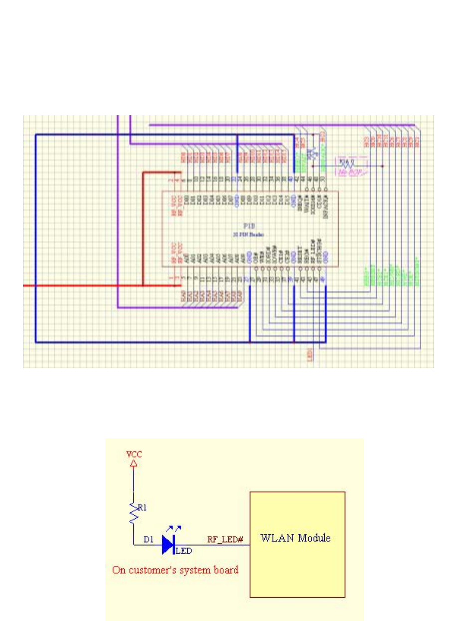
2.0 Pin Define Circuit Diagram:
2.1 LED connection suggestion:
6/9 Version 1.1
ඔ碁ઝݾैٝڶૻֆ
No. 10-1 , Li-hsin Road I
Science-based Industrial Park ,
Hsinchu 300,Taiwan, R.O.C.
Tel: 886-3-6667799
Fax: 886-3-6667711
Web site: www.wneweb.com
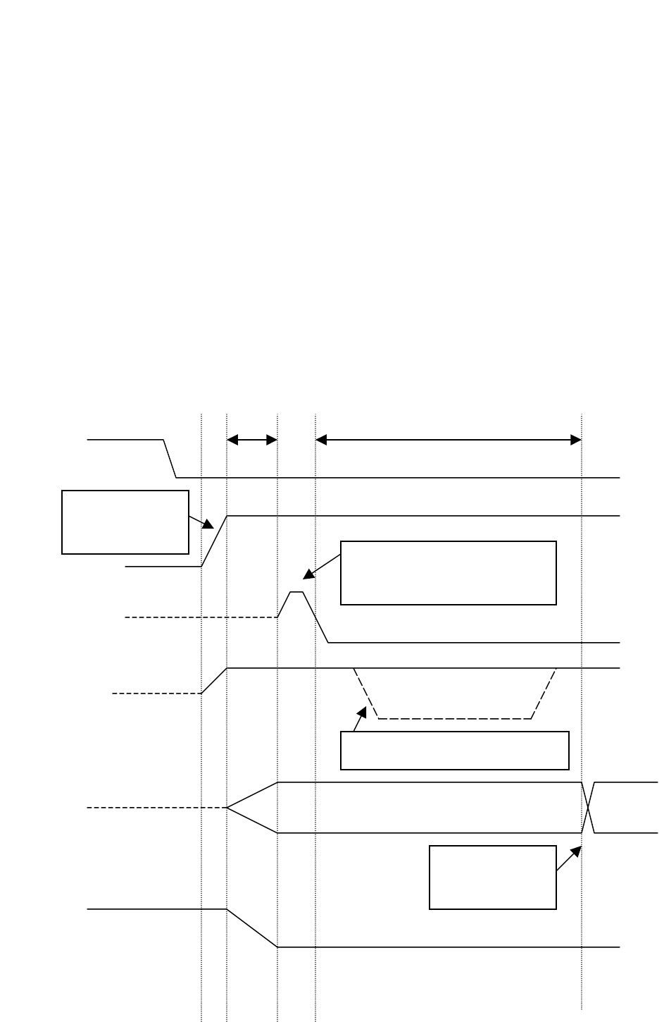
3.0 Timing Specification:
3.1 Power On Reset Configuration:
Power on reset was issued from Host to the ISL3871IK18 MAC/BB through the
RESET pin or via the soft reset bit. The Host system applies RESET at least [1ms
after VCC has reached 90% of its end value] and the hold time is at least 1ms. (see
PC-Card standard, Vol.2, CH.4.12.1). Please see ISL3871IK18 MAC/BB datasheet
page 20 for the detail.
3.2 WLAN module initial procedure:
48 CD1#
41 RESET
42 IREQ#
Interface
signal
1,2,3,4, RF_VCC
>1ms >20ms
Rising time between
0.1ms to 300ms
RESET at least 1ms after VCC
has reached 90% of its value
If WLAN is not ready in 20ms
WLAN module is
ready
System
Buffer_EN#
7/9 Version 1.1
ඔ碁ઝݾैٝڶૻֆ
No. 10-1 , Li-hsin Road I
Science-based Industrial Park ,
Hsinchu 300,Taiwan, R.O.C.
Tel: 886-3-6667799
Fax: 886-3-6667711
Web site: www.wneweb.com
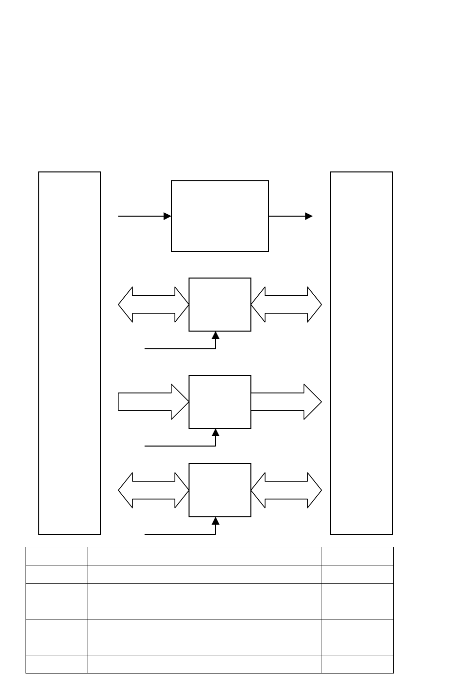
3.3 Suggestion:
All interface of Host to MAC/BB (control pin, address bus, data bus…) need to add
tri-state buffers in system side. To avoid the latch-up appearance this method should be
implemented.
For Example:
Signal Pin Number Total Pins
RF_VCC 1,2,3,4 4
Control
signals
27,29,31,33,35,37,41,42,43,44,45,46,47,48,50 15
Address
Bus
5,7,9,11,13,15,17,19,21,23 10
Data Bus 6,8,10,12,14,16,18,20,24,26,28,30,32,34,36,38 16
Buffer IC
Control
Signals
PDA
Host
System
Control
Signals WLAN
CF
module
Buffer IC
Address
Bus
Address
Bus
Buffer IC
Data
Bus
Data
Bus
Regulator
(500mA@3.3V)
RF_VCC
WLAN
POWER
SWITCH
Buffer_EN#
Buffer_EN#
Buffer_EN#

8/9 Version 1.1
ඔ碁ઝݾैٝڶૻֆ
No. 10-1 , Li-hsin Road I
Science-based Industrial Park ,
Hsinchu 300,Taiwan, R.O.C.
Tel: 886-3-6667799
Fax: 886-3-6667711
Web site: www.wneweb.com
4.0 Brief specification:
z Frequency band: 2400 ~ 2483.5 MHz (for US, Canada, and ETSI)
2471 ~ 2497 MHz (for Japan)
z Channel Spacing 5MHz
z Modulation: DSSS with DBPSK, DQPSK, and CCK
z Host interface: (Proprietary) CF V1.4
z Channels Support: US/Canada: 11 (1~11)
ETSI: 13 (1~13)
France: 4 (10~13)
Japan: 14 (1~14)
z Supply Voltage: 3.3±5% DC
z Current Consumption: Tx: 280mA (typical)~310mA (max)
Rx: 260mA (typical)~290mA (max)
Idle: 230 (typical)~270mA (max)
Power saving: 25mA (typical)~40mA (max)
z Radio Power: +14.59dBm
z Sensitivity: -82±1dBm @ 11Mbps
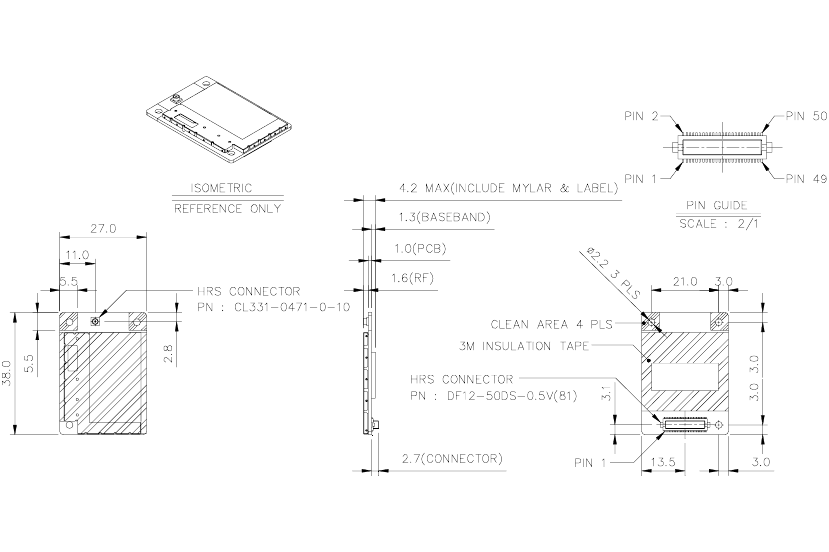
4.1 Mechanical Diagram: see attachment (for reference)
Country Code selection feature to be disabled for products marketed to the US/CANADA
AREA
BASEBAND
LABEL
Federal Communication Commission Interference Statement
This equipment has been tested and found to comply with the limits for a Class B digital device, pursuant
to Part 15 of the FCC Rules. These limits are designed to provide reasonable protection against harmful
interference in a residential installation. This equipment generates, uses and can radiate radio frequency
energy and, if not installed and used in accordance with the instructions, may cause harmful interference
to radio communications. However, there is no guarantee that interference will not occur in a particular
installation. If this equipment does cause harmful interference to radio or television reception, which can
be determined by turning the equipment off and on, the user is encouraged to try to correct the interference
by one of the following measures:
- Reorient or relocate the receiving antenna.
- Increase the separation between the equipment and receiver.
- Connect the equipment into an outlet on a circuit different from that to which the receiver is
connected.
- Consult the dealer or an experienced radio/TV technician for help.
FCC Caution: Any changes or modifications not expressly approved by the party responsible for
compliance could void the user's authority to operate this equipment.
This device complies with Part 15 of the FCC Rules. Operation is subject to the following two conditions: (1)
This device may not cause harmful interference, and (2) this device must accept any interference received,
including interference that may cause undesired operation.
IMPORTANT NOTE: FCC Radiation Exposure Statement:
This equipment complies with FCC radiation exposure limits set forth for an uncontrolled environment.
In order to avoid the possibility of exceeding the FCC radio frequency exposure limits, human proximity
to the antenna shall not be less than 20cm (8 inches) during normal operation.
This device can not be worn on the body and at least keep it 20 cm away from body parts other than
hand, wrists, feet and ankles.
The antenna used for this transmitter must not be colocated or operating in conjunction with any other
transmitter/antenna except CIPHERLAB 8300 series terminal.
The OEM integrator will be responsible for re-evaluating the end product (including the transmitter) and
obtaining a separate FCC authorization.
The final end product must be labeled in a visible area with the following:
“Contains TX FCC ID: Q3N-8300W”.
This device complies with Part 15 of the FCC Rules. Operation is subject to the following two conditions: (1)
This device may not cause harmful interference, and (2) this device must accept any interference received,
including interference that may cause undesired operation.
The OEM integrator is still responsible for testing their end-product for any additional compliance requirements
required with this module installed (for example, digital device emissions, PC peripheral requirements, etc.).
Limited Module Approval Statement:
This device is intended only for OEM Integrators.The module should be equipped within CIPHERLAB 8XXX
series terminal.