Compal Electronics CAX00NFC NFC Controller Module with Antenna User Manual Module
Compal Electronics Inc NFC Controller Module with Antenna Module
Contents
- 1. User Manual
- 2. User Manual(Module)
- 3. User Manual (Module)
User Manual(Module)

SM-MMN17-C01
NFC Controller Module with Antenna
Datasheet Version 1.2
Smart Approach Co., Ltd.
Rm. 5, 3F., No.1, Taiyuan 2nd St.,
Zhubei City, Hsinchu County 302,
Taiwan, R.O.C.
+886-3-5601363
www.smart-approach.com.tw
SM-MMN17-C01 Datasheet
-
2 -
Revision 1.2 October 2016
Smart Approach Co., Ltd ( S.A. ) retains the right to make changes to its products or
specifications to improve performance, reliability or manufacturability. All information in this
document, including descriptions of features, functions, performance, technical specifications
and availability, is subject to change without notice at any time. While the information furnished
herein is held to be accurate and reliable, no responsibility will be assumed by Smart Approach
for its use. Furthermore, the information contained herein does not convey to the purchaser of
microelectronic devices any license under license under the patent right of any manufacturer.
Smart Approach Co., Ltd is a registered trademark. All other products or service names used in
this publication are for identification purposes only, and may be trademarks or registered
trademarks of their respective companies. All other trademarks or registered trademarks
mentioned herein are the property of their respective holders.
Feedback on the use of any of the document is welcomed and encouraged by Smart
Approach.
Please contact service@smart-approach.com.tw for your feedback or any ordering
inquiry.
Please contact support@smart-approach.com.tw for any technical question.
This section describes the changes that were implemented in this document. The changes are
listed by revision, starting with the most current publication.
Revision 1.0
Revision 1.0 of this datasheet was published in December 2014. This was the first publication
of the document.
Revision 1.1
Updated chapter 2 features, in April 2016.
Revision 1.2
Updated chapter 7 outline, in October 2016.
SM-MMN17-C01 Datasheet
-
3 -
Revision 1.2 October 2016
REVISION HISTORY ............................................................................................................................. - 2 -
CONTENTS ........................................................................................................................................... - 3 -
FIGURE CONTENTS ............................................................................................................................ - 4 -
TABLE CONTENTS .............................................................................................................................. - 4 -
1 INTRODUCTION .......................................................................................................................... - 5 -
2 PRODUCT OVERVIEW ................................................................................................................ - 6 -
2.1 F
EATURES
.............................................................................................................................. -
6
-
2.2 A
PPLICATION
.......................................................................................................................... -
6
-
3 FUNCTIONAL DESCRIPTIONS .................................................................................................. - 7 -
4 ELECTRICAL SPECIFICATIONS ................................................................................................ - 8 -
4.1 P
IN
D
ESCRIPTION
................................................................................................................... -
8
-
4.2 I2C
A
DDRESS
......................................................................................................................... -
9
-
4.3 T
EMPERATURE
M
AXIMUM
R
ATINGS
.......................................................................................... -
9
-
4.4 DC
E
LECTRICAL
P
ARAMETERS
.............................................................................................. -
10
-
4.5 A
NTENNA
S
PECIFICATION
...................................................................................................... -
10
-
4.6 P
OWER
C
ONSUMPTION
.......................................................................................................... -
11
-
4.7 T
HERMAL
P
ROTECTION
.......................................................................................................... -
11
-
4.8 S
YSTEM POWER MODES
......................................................................................................... -
11
-
4.9 R
ESET AND DOWNLOAD CONCEPT
.......................................................................................... -
12
-
5 ORDERING INFORMATION ...................................................................................................... - 13 -
6 RELIABILITY VERIFICATION .................................................................................................... - 14 -
7 NFC MODULE OUTLINE ........................................................................................................... - 15 -
SM-MMN17-C01 Datasheet
-
4 -
Revision 1.2 October 2016
Figure 1 Typical Application ................................................................................................. - 6 -
Figure 2 Module Block Diagram .......................................................................................... - 7 -
Figure 3 Reset via V
EN
pin ................................................................................................. - 12 -
Figure 4 NFC Module Drawing .......................................................................................... - 15 -
Figure 5 Module FPC Connection Foot Print ..................................................................... - 16 -
Figure 6 FPC Wire Dimension ........................................................................................... - 16 -
Table 1 Module Pin Description ........................................................................................... - 8 -
Table 2 I
2
C Address ............................................................................................................. - 9 -
Table 3 Temperature Maximum Ratings .............................................................................. - 9 -
Table 4 DC Electrical Specification .................................................................................... - 10 -
Table 5 Antenna Specifications .......................................................................................... - 10 -
Table 6 Current Consumption ............................................................................................ - 11 -
Table 7 Thermal Protection ................................................................................................ - 11 -
Table 8 System Power Modes Description ........................................................................ - 11 -
Table 9 Power Mode Configuration .................................................................................... - 12 -
Table 10 Reset Timing ....................................................................................................... - 12 -
Table 11 Ordering Information Table .................................................................................. - 13 -
Table 12 Reliability Item Table ........................................................................................... - 14 -

SM-MMN17-C01 Datasheet
-
5 -
Revision 1.2 October 2016
1 Introduction
This document consists of descriptions and specifications for both functional and physical
aspects of the SM-MMN17-C01 NFC reader / writer module.
In addition to the datasheet, Smart Approach maintains and extensive device-specific library of
support and collateral materials that you may find useful in your application. Depending upon
the Smart Approach device, this library may include:
Presentations highlighting the operational features and specifications of the device to
assist in developing your own product road map.
Application notes that provide detailed descriptions of the use of the particular Smart
Approach product to solve real-world problems.
SM-MMN17-C01 Datasheet
-
6 -
Revision 1.2 October 2016
2 Product Overview
SM-MMN17-C01 is full featured NFC controllers designed for integration in portable equipment.
It is optimized for low power consumption with fully host controllable power states and for small
footprint for portable equipment applications.
size-sensitive
applications, assures robust performance.
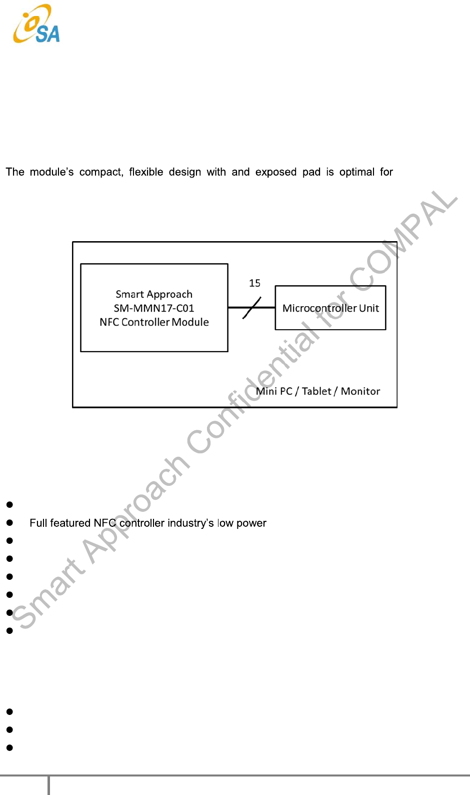
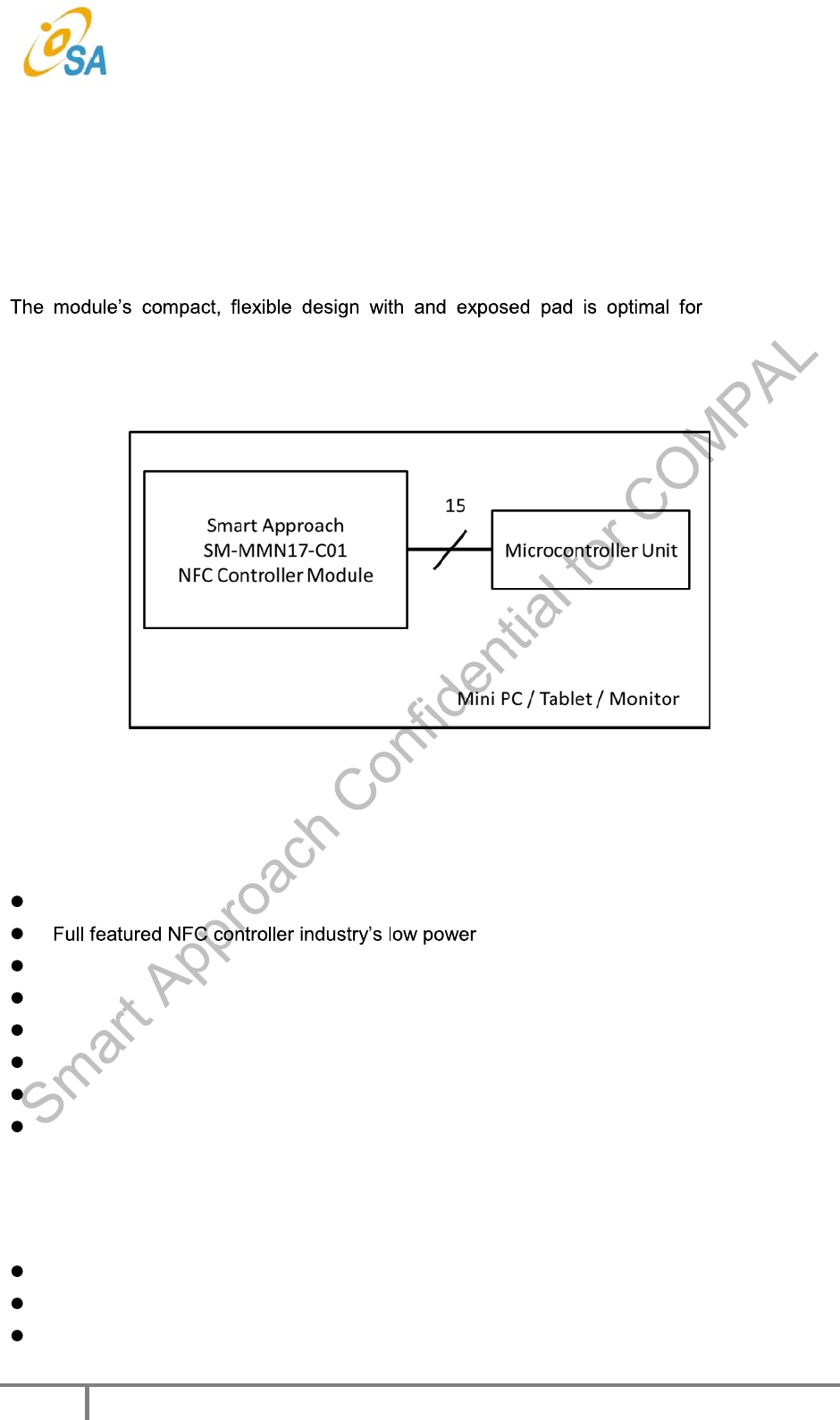
The following illustration shows a high-level, generic view of a SM-MMN17-C01 application.
Figure 1 Typical Application
2.1 Features
This section Tables key aspects of the SM-MMN17-C01 module functionality and design that
distinguish it from similar products:
NXP NPC100
consumption.
Compliant with ISO/IEC 14443 A/B
Compliant with ISO/IEC 15693/18092
Compliant with NFCIP-1, NFCIP-2
Support MIFARE and Felica specifications
Customized antenna pairing
I
2
C interface
2.2 Application
Suggested applications for the SM-MMN17-C01 module include:
NFC writer/ reader
NFC peer to peer controller
NFC identification

SM-MMN17-C01 Datasheet
-
7 -
Revision 1.2 October 2016
3 Functional Descriptions
This section provides detailed information about how SM-MMN17-C01 module works, what
configurations and operational features are available.
The following illustration shows the primary functional blocks of SM-MMN17-C01 module.
Figure 2 Module Block Diagram
Loop Antenna is Smart Approach customize solution. Antenna matching is also a customize
solution. NFC controller includes NXP NPC100 chipset, and has an I
2
C control interface
through the connector to mother board.
Customized Antenna

SM-MMN17-C01 Datasheet
-
8 -
Revision 1.2 October 2016
4 Electrical Specifications
This section provides the DC characteristics, AC characteristics, recommended operating
conditions. It includes information on the various timing functions of the module.
4.1 Pin Description
The following Table shows the pin description for SM-MMN17-C01 module.
The connection ground is internally connected and should be connected to GND on the main
board as well.
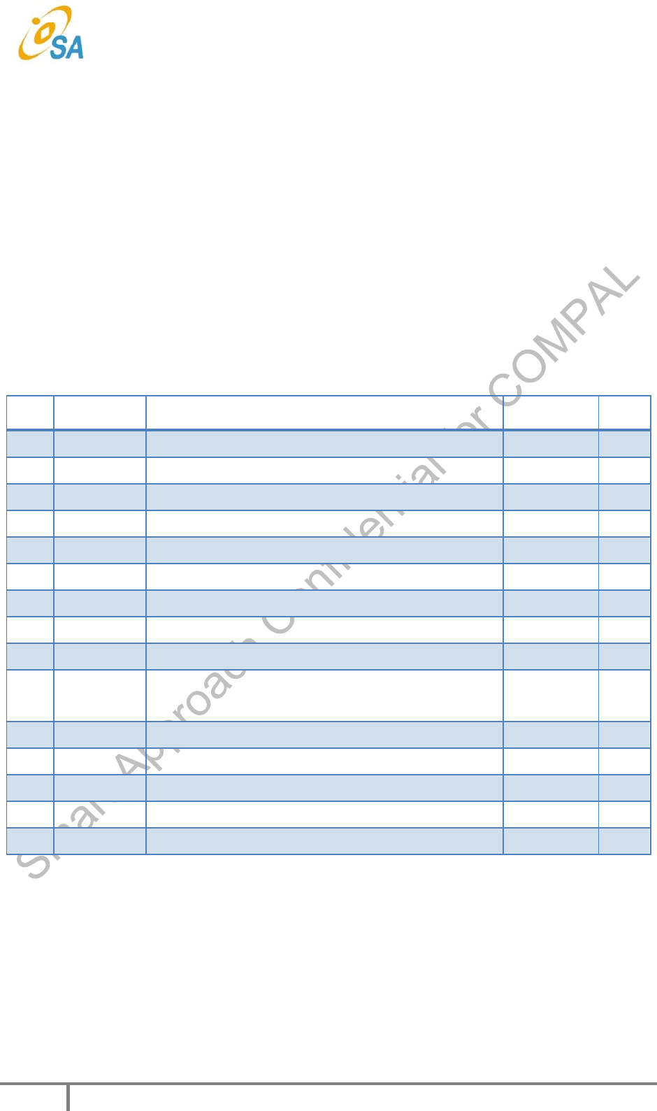
Table 1 Module Pin Description
PIN
No. Name Description Power
Reference P/I/O
1 VBAT +3.3V power supply input 3.3V P
2 MOD_GND Module Ground GND P
3 SWP SWP data line to UICC/SIM, Input / Output PMUVCC I/O
4 RFU Unused pin could be floating - -
5 IRQ Interrupt to host, High: Interrupt; Low: Normal VDD_IO O
6 PMUVCC Power supply to UICC/SIM, input, + 1.8V 1.8V P
7 I2C_SDA I2C Data Line (400Kbps) VDD_IO I/O
8 I2C_SCL I2C Clock (400Kbps) VDD_IO I
9 MOD_GND Module Ground GND P
10 VEN Wake up the module from standby mode or reset the
module VBAT I
11 DWL_REQ Firmware download control: Active High VDD_IO I
12 SIMVCC The power rail used to power UICC / SIM, output pin PMUVCC P(O)
13 VBAT +3.3V Power Supply 3.3V P
14 VDD_IO +1.8V or +3.3V for host IO reference voltage 1.8V/3.3V P
15 MOD_GND Module Ground GND P
SM-MMN17-C01 Datasheet
-
9 -
Revision 1.2 October 2016
4.2 I
2
C Address
SM-MMN17-C01 I
2
C 7bit address is defined to 0x28. To write data, the module is addressed
using 0x50, to read data, the module is addressed using 0x51.
Table 2 I
2
C Address
I2C address (R/W=0, write) I2C address (R/W=1, read)
0x50 0x51
4.3 Temperature Maximum Ratings
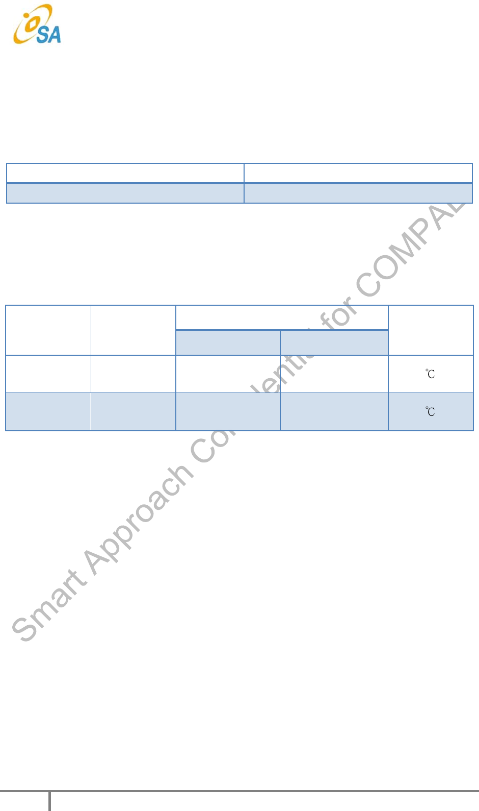
Thermal specifications for this module have been modeled using a two-layer test board.
Table 3 Temperature Maximum Ratings
Symbol Definition Value Units
Min Max
T Operating
Temperature -20 80
T
S
Storage
Temperature -40 100

SM-MMN17-C01 Datasheet
-
10 -
Revision 1.2 October 2016
4.4 DC Electrical Parameters
DC Electrical specifications for this module have been modeled using a two-layer test board.
Table 4 DC Electrical Specification
Symbol Definition Value Units
Min Typ Max
V
BAT
Power
Supply 3.1 3.3 3.5 Volts
I
VBAT
DC Current 170 mA
4.5 Antenna Specification
Antenna specifications for this module have been modeled using a two-layer test board.
Table 5 Antenna Specifications
Item
Value
Unit Note
Min Type Max
DC
Resistance 0.5 1 2
AC
Impedance 50
Frequency 13.06 13.56 14.06 MHz
VSWR <2
Q factor 25 30 35
SM-MMN17-C01 Datasheet
-
11 -
Revision 1.2 October 2016
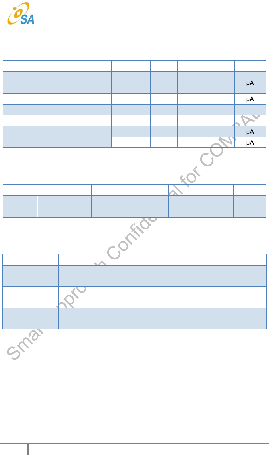
4.6 Power Consumption
Table 6 Current Consumption
Symbol Parameter Conditions Min Typ Max Unit
I
HPD
Hard power down current V
BAT
=3.6V,
V
EN
=0V - 10.5 12
I
STBY
Standby state current V
BAT
=3.6V - - 20
I
ACT
Active state current V
BAT
=3.6V - 6 - mA
I
TVDD
Transmitter supply current V
BAT
=3.1V - 30 100 mA
I
PMUVCC
PMUVCC supply Class B - 1.5 3
Class C - 1 2
4.7 Thermal Protection
Table 7 Thermal Protection
Symbol Parameter Conditions Min Typ Max Unit
T
OVERTEMP
Temperature
protection trigger 120 125 130
0
C
4.8 System power modes
Table 8 System Power Modes Description
Mode Description
Full power
mode
The battery supply (V
BAT
) as well as the pad supply (VDD_IO) is
available, all use cases can be executed
Low-power
mode
The pad supply (VDD_IO) is not available. Only the Card Emulation
mode use cases via SWP are allowed
Power Off mode The system is not supplied from any source or the system is kept Hard
Power Down (HPD)

SM-MMN17-C01 Datasheet
-
12 -
Revision 1.2 October 2016
Table 9 Power Mode Configuration
V
BAT
VDD_IO V
EN
Power mode
Off Off X Power Off mode
On X Off Power Off mode
On Off On Low Power Mode
On On On Full power mode
Note: X: Don t care
4.9 Reset and download concept
To enter reset there are 2 ways:
- Pulling V
EN
low (Hard Power Down state)
- If V
BAT
monitor is enabled: lowering V
BAT
below the monitor threshold (monitor mode, if V
EN
is kept above 1.1 V)
To get out of reset, there are 1 ways:
- Pulling V
EN
high with V
BAT
above V
BAT
monitor threshold if enabled
Figure 3 Reset via V
EN
pin
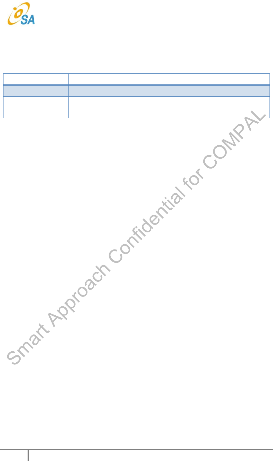
Table 10 Reset Timing
Symbol Parameter Condition Min Typ Max Unit
t
RESETVEN
V
EN
pulse
width to reset 3
t
BOOT
Boot time 10 ms
SM-MMN17-C01 Datasheet
-
13 -
Revision 1.2 October 2016
5 Ordering Information
Table 11 Ordering Information Table
Order Number Descriptions
SM-MMN17-C01 NFC Controller Module (NXP NPC100) with Antenna
Dimension Module: 26.65x10.00 mm; Antenna Area: 32.00x10.00mm
Total Size: 63.65x10.00mm
SM-MMN17-C01 Datasheet
-
14 -
Revision 1.2 October 2016
6 Reliability Verification
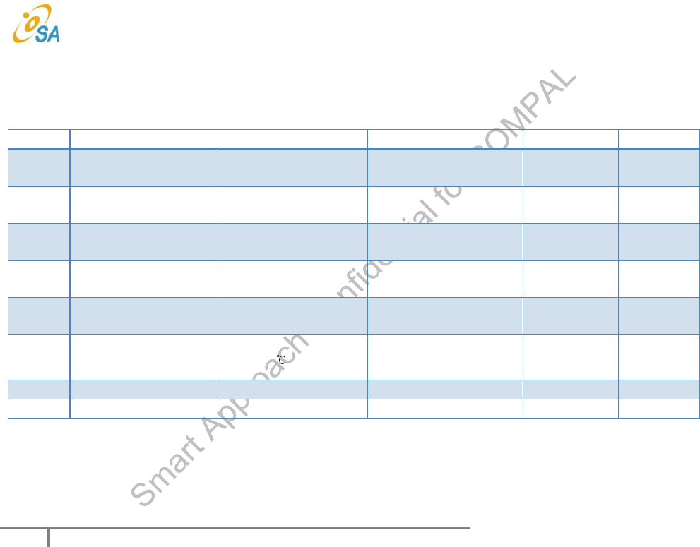
Table 12 Reliability Item Table
No. Item Condition Benchmark Result Qty
1 Low Temperature Storage
Test -40
o
C IEC60068-2-1 Pass 5
2 High Temperature Storage
Test 80
o
C, Humidity: 95% IEC60068-2-78 Pass 5
3 Low Temperature Operation
Test -20
o
C IEC60068-2-1 Pass 5
4 High Temperature Operation
Test 80
o
C IEC60068-2-2 Pass 5
5 High Temperature Operation
Test 65
o
C, Humidity: 95% IEC60068-2-78 Pass 5
6 Salt Test
PH: 3.0 ~ 3.2
,50 , 72 hrs,
Density: 5%±1%
ASTM B368 Pass 5
7 RoHS Normal Compliance Pass 5
8 HF Normal Compliance Pass 5
SM-MMN17-C01 Datasheet
-
15 -
Revision 1.2 October 2016
7 NFC Module Outline
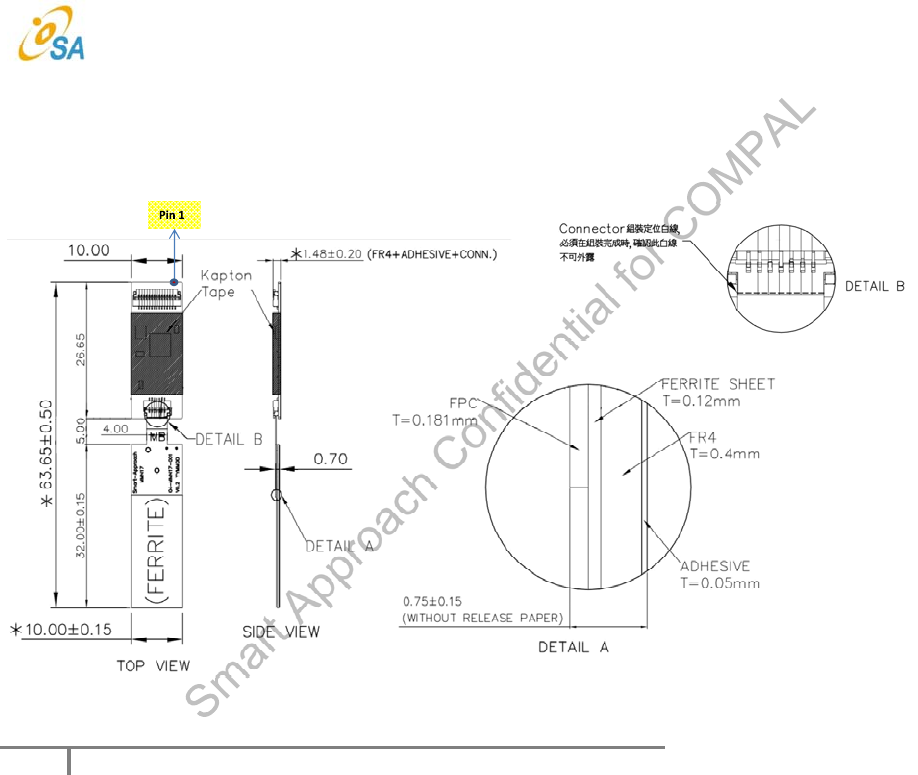
The following illustration shows the package drawing for SM-MMN17-C01 module. The drawing contains the detail views, dimensions,
tolerances, and notes.
Figure 4 NFC Module Drawing
SM-MMN17-C01 Datasheet
-
16 -
Revision 1.2 October 2016
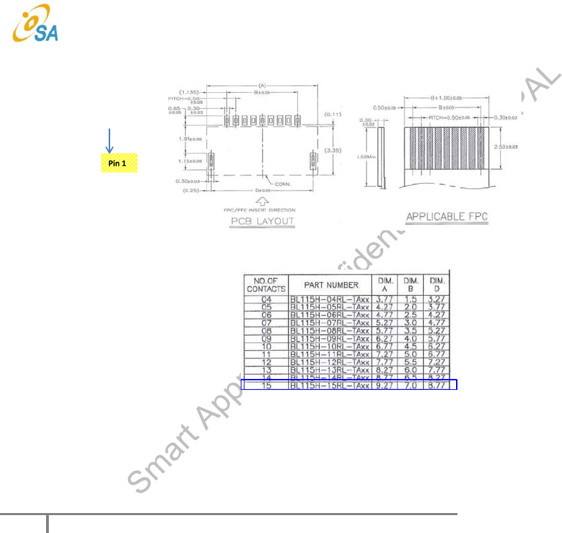
Figure 5 Module FPC Connection Foot Print
Figure 6 FPC Wire Dimension
Federal Communication Commission Interference Statement
This device complies with Part 15 of the FCC Rules. Operation is subject to the
following two conditions: (1) This device may not cause harmful interference, and (2)
this device must accept any interference received, including interference that may
cause undesired operation.
This equipment has been tested and found to comply with the limits for a Class B
digital device, pursuant to Part 15 of the FCC Rules. These limits are designed to
provide reasonable protection against harmful interference in a residential
installation. This equipment generates, uses and can radiate radio frequency energy
and, if not installed and used in accordance with the instructions, may cause harmful
interference to radio communications. However, there is no guarantee that
interference will not occur in a particular installation. If this equipment does cause
harmful interference to radio or television reception, which can be determined by
turning the equipment off and on, the user is encouraged to try to correct the
interference by one of the following measures:
Reorient or relocate the receiving antenna.
Increase the separation between the equipment and receiver.
Connect the equipment into an outlet on a circuit different from that
to which the receiver is connected.
Consult the dealer or an experienced radio/TV technician for help.
FCC Caution:
Any changes or modifications not expressly approved by the party responsible
for compliance could void the user's authority to operate this equipment.
This transmitter must not be co-located or operating in conjunction with any
other antenna or transmitter.

Radiation Exposure Statement:
The product is a low power device and its output power is lower than FCC SAR
exemption level. This module can be used with SM-MMN17-C01.
This device is intended only for OEM integrators under the following conditions:
1) The transmitter module may not be co-located with any other transmitter or
antenna. The co-transmitting with other radio will need a separate evaluation.
2) Module approval valid only when this module is installed in the tested host
“CAX00, CXXXXX-CAX00-XXXXXX-XXXX (X:0~9,A~Z)”.
As long as 2 conditions above are met, further transmitter test will not be required.
However, the OEM integrator is still responsible for testing their end-product for any
additional compliance requirements required with this module installed
IMPORTANT NOTE: In the event that these conditions cannot be met (for example
certain laptop configurations or co-location with another transmitter), then the FCC
authorization is no longer considered valid and the FCC ID cannot be used on the
final product. In these circumstances, the OEM integrator will be responsible for
re-evaluating the end product (including the transmitter) and obtaining a separate
FCC authorization.
End Product Labeling
The final end product must be labeled in a visible area with the following: “Contains
FCC ID: GKR-CAX00NFC”. The grantee's FCC ID can be used only when all FCC
compliance requirements are met.
Manual Information to the End User
The OEM integrator has to be aware not to provide information to the end user
regarding how to install or remove this RF module in the user’s manual of the end
product which integrates this module.
The end user manual shall include all required regulatory information/warning as
show in this manual.
Industry Canada statement
This device complies with Industry Canada license-exempt RSS standard(s).
Operation is subject to the following two conditions:
1) this device may not cause interference, and
2) this device must accept any interference, including interference that may
cause undesired operation of the device.
Le présent appareil est conforme aux CNR d'Industrie Canada applicables aux
appareils radio exempts de licence. L'exploitation est autorisée aux deux
conditions suivantes:
1) l'appareil ne doit pas produire de brouillage, et
2) l'utilisateur de l'appareil doit accepter tout brouillage radioélectrique subi,
même si le brouillage est susceptible d'en compromettre le
fonctionnement.
This Class B digital apparatus complies with Canadian ICES-003.
Cet appareil numérique de la classe B est conforme à la norme NMB-003 du
Canada.
This device and its antenna(s) must not be co-located or operating in
conjunction with any other antenna or transmitter, except tested built-in
radios.
Cet appareil et son antenne ne doivent pas être situés ou fonctionner en
conjonction avec une autre antenne ou un autre émetteur, exception faites des
radios intégrées qui ont été testées.
This device is intended only for OEM integrators under the following conditions:
(For module device use)
1) The transmitter module may not be co-located with any other transmitter or
antenna.
As long as one condition above is met, further transmitter test will not be required.
However, the OEM integrator is still responsible for testing their end-product for any
additional compliance requirements required with this module installed.
Cet appareil est conçu uniquement pour les intégrateurs OEM dans les conditions
suivantes: (Pour utilisation de dispositif module)
1) Le module émetteur peut ne pas être coïmplanté avec un autre émetteur ou
antenne.
Tant qu'une condition ci-dessus est remplie, un autre test de l'émetteur n'est pas
nécessaire. Toutefois, l'intégrateur OEM est toujours responsable de tester leur
produit final pour toutes les exigences de conformité supplémentaires requises avec
ce module installé.
IMPORTANT NOTE:
In the event that these conditions cannot be met (for example certain laptop
configurations or co-location with another transmitter), then the Canada
authorization is no longer considered valid and the IC ID cannot be used on the final
product. In these circumstances, the OEM integrator will be responsible for
re-evaluating the end product (including the transmitter) and obtaining a separate
Canada authorization.
NOTE IMPORTANTE:
Dans le cas où ces conditions ne peuvent être satisfaites (par exemple pour certaines
configurations d'ordinateur portable ou de certaines co-localisation avec un autre
émetteur), l'autorisation du Canada n'est plus considéré comme valide et l'ID IC ne
peut pas être utilisé sur le produit final. Dans ces circonstances, l'intégrateur OEM
sera chargé de réévaluer le produit final (y compris l'émetteur) et l'obtention d'une
autorisation distincte au Canada.
End Product Labeling
The product can be kept as far as possible from the user body or set the device to
lower output power if such function is available. The final end product must be
labeled in a visible area with the following: “Contains IC: 2533B-CAX00NFC”.
Plaque signalétique du produit final
L'appareil peut être conservé aussi loin que possible du corps de l'utilisateur ou que
le dispositif est réglé sur la puissance de sortie la plus faible si une telle fonction est
disponible. Le produit final doit être étiqueté dans un endroit visible avec
l'inscription suivante: "Contient des IC: 2533B-CAX00NFC".
Manual Information To the End User
The OEM integrator has to be aware not to provide information to the end user
regarding how to install or remove this RF module in the user’s manual of the end
product which integrates this module.
The end user manual shall include all required regulatory information/warning as
show in this manual.
Manuel d'information à l'utilisateur final
L'intégrateur OEM doit être conscient de ne pas fournir des informations à
l'utilisateur final quant à la façon d'installer ou de supprimer ce module RF dans le
manuel de l'utilisateur du produit final qui intègre ce module.
Le manuel de l'utilisateur final doit inclure toutes les informations réglementaires
requises et avertissements comme indiqué dans ce manuel.
User Manual (Module)

SM-MMN17-C01
NFC Controller Module with Antenna
Datasheet Version 1.2
Smart Approach Co., Ltd.
Rm. 5, 3F., No.1, Taiyuan 2nd St.,
Zhubei City, Hsinchu County 302,
Taiwan, R.O.C.
+886-3-5601363
www.smart-approach.com.tw

SM-MMN17-C01 Datasheet
-
2 -
Revision 1.2 October 2016
Smart Approach Co., Ltd ( S.A. ) retains the right to make changes to its products or
specifications to improve performance, reliability or manufacturability. All information in this
document, including descriptions of features, functions, performance, technical specifications
and availability, is subject to change without notice at any time. While the information furnished
herein is held to be accurate and reliable, no responsibility will be assumed by Smart Approach
for its use. Furthermore, the information contained herein does not convey to the purchaser of
microelectronic devices any license under license under the patent right of any manufacturer.
Smart Approach Co., Ltd is a registered trademark. All other products or service names used in
this publication are for identification purposes only, and may be trademarks or registered
trademarks of their respective companies. All other trademarks or registered trademarks
mentioned herein are the property of their respective holders.
Feedback on the use of any of the document is welcomed and encouraged by Smart
Approach.
Please contact service@smart-approach.com.tw for your feedback or any ordering
inquiry.
Please contact support@smart-approach.com.tw for any technical question.
This section describes the changes that were implemented in this document. The changes are
listed by revision, starting with the most current publication.
Revision 1.0
Revision 1.0 of this datasheet was published in December 2014. This was the first publication
of the document.
Revision 1.1
Updated chapter 2 features, in April 2016.
Revision 1.2
Updated chapter 7 outline, in October 2016.

SM-MMN17-C01 Datasheet
-
3 -
Revision 1.2 October 2016
REVISION HISTORY ............................................................................................................................. - 2 -
CONTENTS ........................................................................................................................................... - 3 -
FIGURE CONTENTS ............................................................................................................................ - 4 -
TABLE CONTENTS .............................................................................................................................. - 4 -
1 INTRODUCTION .......................................................................................................................... - 5 -
2 PRODUCT OVERVIEW ................................................................................................................ - 6 -
2.1 F
EATURES
.............................................................................................................................. -
6
-
2.2 A
PPLICATION
.......................................................................................................................... -
6
-
3 FUNCTIONAL DESCRIPTIONS .................................................................................................. - 7 -
4 ELECTRICAL SPECIFICATIONS ................................................................................................ - 8 -
4.1 P
IN
D
ESCRIPTION
................................................................................................................... -
8
-
4.2 I2C
A
DDRESS
......................................................................................................................... -
9
-
4.3 T
EMPERATURE
M
AXIMUM
R
ATINGS
.......................................................................................... -
9
-
4.4 DC
E
LECTRICAL
P
ARAMETERS
.............................................................................................. -
10
-
4.5 A
NTENNA
S
PECIFICATION
...................................................................................................... -
10
-
4.6 P
OWER
C
ONSUMPTION
.......................................................................................................... -
11
-
4.7 T
HERMAL
P
ROTECTION
.......................................................................................................... -
11
-
4.8 S
YSTEM POWER MODES
......................................................................................................... -
11
-
4.9 R
ESET AND DOWNLOAD CONCEPT
.......................................................................................... -
12
-
5 ORDERING INFORMATION ...................................................................................................... - 13 -
6 RELIABILITY VERIFICATION .................................................................................................... - 14 -
7 NFC MODULE OUTLINE ........................................................................................................... - 15 -

SM-MMN17-C01 Datasheet
-
4 -
Revision 1.2 October 2016
Figure 1 Typical Application ................................................................................................. - 6 -
Figure 2 Module Block Diagram .......................................................................................... - 7 -
Figure 3 Reset via V
EN
pin ................................................................................................. - 12 -
Figure 4 NFC Module Drawing .......................................................................................... - 15 -
Figure 5 Module FPC Connection Foot Print ..................................................................... - 16 -
Figure 6 FPC Wire Dimension ........................................................................................... - 16 -
Table 1 Module Pin Description ........................................................................................... - 8 -
Table 2 I
2
C Address ............................................................................................................. - 9 -
Table 3 Temperature Maximum Ratings .............................................................................. - 9 -
Table 4 DC Electrical Specification .................................................................................... - 10 -
Table 5 Antenna Specifications .......................................................................................... - 10 -
Table 6 Current Consumption ............................................................................................ - 11 -
Table 7 Thermal Protection ................................................................................................ - 11 -
Table 8 System Power Modes Description ........................................................................ - 11 -
Table 9 Power Mode Configuration .................................................................................... - 12 -
Table 10 Reset Timing ....................................................................................................... - 12 -
Table 11 Ordering Information Table .................................................................................. - 13 -
Table 12 Reliability Item Table ........................................................................................... - 14 -
SM-MMN17-C01 Datasheet
-
5 -
Revision 1.2 October 2016
1 Introduction
This document consists of descriptions and specifications for both functional and physical
aspects of the SM-MMN17-C01 NFC reader / writer module.
In addition to the datasheet, Smart Approach maintains and extensive device-specific library of
support and collateral materials that you may find useful in your application. Depending upon
the Smart Approach device, this library may include:
Presentations highlighting the operational features and specifications of the device to
assist in developing your own product road map.
Application notes that provide detailed descriptions of the use of the particular Smart
Approach product to solve real-world problems.
SM-MMN17-C01 Datasheet
-
6 -
Revision 1.2 October 2016
2 Product Overview
SM-MMN17-C01 is full featured NFC controllers designed for integration in portable equipment.
It is optimized for low power consumption with fully host controllable power states and for small
footprint for portable equipment applications.
size-sensitive
applications, assures robust performance.
The following illustration shows a high-level, generic view of a SM-MMN17-C01 application.
Figure 1 Typical Application
2.1 Features
This section Tables key aspects of the SM-MMN17-C01 module functionality and design that
distinguish it from similar products:
NXP NPC100
consumption.
Compliant with ISO/IEC 14443 A/B
Compliant with ISO/IEC 15693/18092
Compliant with NFCIP-1, NFCIP-2
Support MIFARE and Felica specifications
Customized antenna pairing
I
2
C interface
2.2 Application
Suggested applications for the SM-MMN17-C01 module include:
NFC writer/ reader
NFC peer to peer controller
NFC identification

SM-MMN17-C01 Datasheet
-
7 -
Revision 1.2 October 2016
3 Functional Descriptions
This section provides detailed information about how SM-MMN17-C01 module works, what
configurations and operational features are available.
The following illustration shows the primary functional blocks of SM-MMN17-C01 module.
Figure 2 Module Block Diagram
Loop Antenna is Smart Approach customize solution. Antenna matching is also a customize
solution. NFC controller includes NXP NPC100 chipset, and has an I
2
C control interface
through the connector to mother board.
Customized Antenna
SM-MMN17-C01 Datasheet
-
8 -
Revision 1.2 October 2016
4 Electrical Specifications
This section provides the DC characteristics, AC characteristics, recommended operating
conditions. It includes information on the various timing functions of the module.
4.1 Pin Description
The following Table shows the pin description for SM-MMN17-C01 module.
The connection ground is internally connected and should be connected to GND on the main
board as well.
Table 1 Module Pin Description
PIN
No. Name Description Power
Reference P/I/O
1 VBAT +3.3V power supply input 3.3V P
2 MOD_GND Module Ground GND P
3 SWP SWP data line to UICC/SIM, Input / Output PMUVCC I/O
4 RFU Unused pin could be floating - -
5 IRQ Interrupt to host, High: Interrupt; Low: Normal VDD_IO O
6 PMUVCC Power supply to UICC/SIM, input, + 1.8V 1.8V P
7 I2C_SDA I2C Data Line (400Kbps) VDD_IO I/O
8 I2C_SCL I2C Clock (400Kbps) VDD_IO I
9 MOD_GND Module Ground GND P
10 VEN Wake up the module from standby mode or reset the
module VBAT I
11 DWL_REQ Firmware download control: Active High VDD_IO I
12 SIMVCC The power rail used to power UICC / SIM, output pin PMUVCC P(O)
13 VBAT +3.3V Power Supply 3.3V P
14 VDD_IO +1.8V or +3.3V for host IO reference voltage 1.8V/3.3V P
15 MOD_GND Module Ground GND P

SM-MMN17-C01 Datasheet
-
9 -
Revision 1.2 October 2016
4.2 I
2
C Address
SM-MMN17-C01 I
2
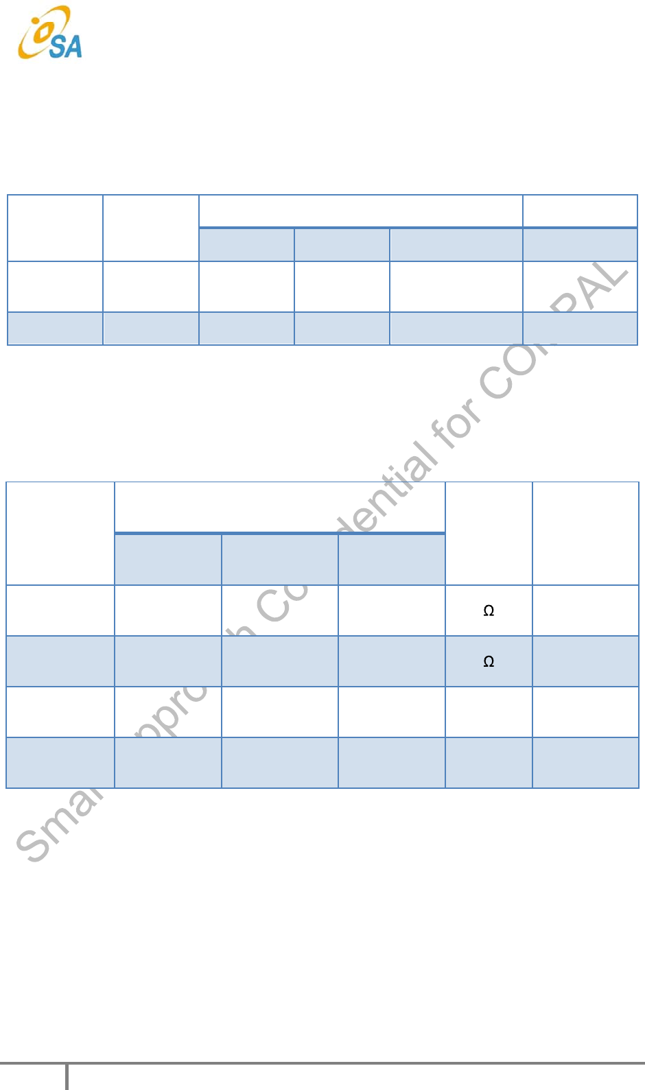
C 7bit address is defined to 0x28. To write data, the module is addressed
using 0x50, to read data, the module is addressed using 0x51.
Table 2 I
2
C Address
I2C address (R/W=0, write) I2C address (R/W=1, read)
0x50 0x51
4.3 Temperature Maximum Ratings
Thermal specifications for this module have been modeled using a two-layer test board.
Table 3 Temperature Maximum Ratings
Symbol Definition Value Units
Min Max
T Operating
Temperature -20 80
T
S
Storage
Temperature -40 100
SM-MMN17-C01 Datasheet
-
10 -
Revision 1.2 October 2016
4.4 DC Electrical Parameters
DC Electrical specifications for this module have been modeled using a two-layer test board.
Table 4 DC Electrical Specification
Symbol Definition Value Units
Min Typ Max
V
BAT
Power
Supply 3.1 3.3 3.5 Volts
I
VBAT
DC Current 170 mA
4.5 Antenna Specification
Antenna specifications for this module have been modeled using a two-layer test board.
Table 5 Antenna Specifications
Item
Value
Unit Note
Min Type Max
DC
Resistance 0.5 1 2
AC
Impedance 50
Frequency 13.06 13.56 14.06 MHz
VSWR <2
Q factor 25 30 35

SM-MMN17-C01 Datasheet
-
11 -
Revision 1.2 October 2016
4.6 Power Consumption
Table 6 Current Consumption
Symbol Parameter Conditions Min Typ Max Unit
I
HPD
Hard power down current V
BAT
=3.6V,
V
EN
=0V - 10.5 12
I
STBY
Standby state current V
BAT
=3.6V - - 20
I
ACT
Active state current V
BAT
=3.6V - 6 - mA
I
TVDD
Transmitter supply current V
BAT
=3.1V - 30 100 mA
I
PMUVCC
PMUVCC supply Class B - 1.5 3
Class C - 1 2
4.7 Thermal Protection
Table 7 Thermal Protection
Symbol Parameter Conditions Min Typ Max Unit
T
OVERTEMP
Temperature
protection trigger 120 125 130
0
C
4.8 System power modes
Table 8 System Power Modes Description
Mode Description
Full power
mode
The battery supply (V
BAT
) as well as the pad supply (VDD_IO) is
available, all use cases can be executed
Low-power
mode
The pad supply (VDD_IO) is not available. Only the Card Emulation
mode use cases via SWP are allowed
Power Off mode The system is not supplied from any source or the system is kept Hard
Power Down (HPD)
SM-MMN17-C01 Datasheet
-
12 -
Revision 1.2 October 2016
Table 9 Power Mode Configuration
V
BAT
VDD_IO V
EN
Power mode
Off Off X Power Off mode
On X Off Power Off mode
On Off On Low Power Mode
On On On Full power mode
Note: X: Don t care
4.9 Reset and download concept
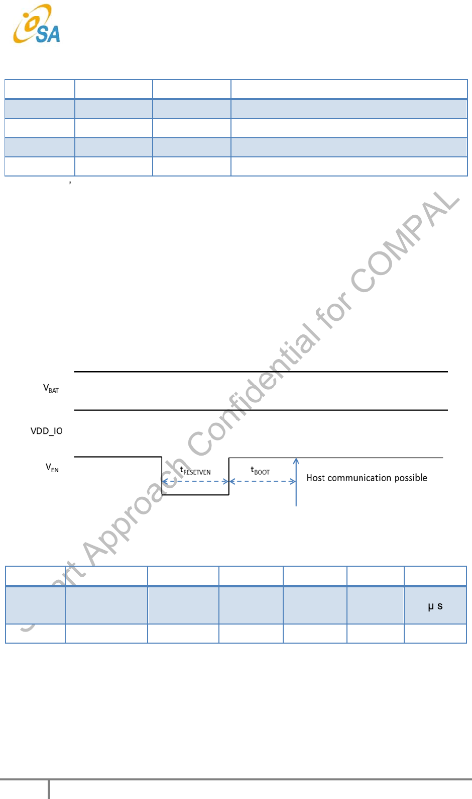
To enter reset there are 2 ways:
- Pulling V
EN
low (Hard Power Down state)
- If V
BAT
monitor is enabled: lowering V
BAT
below the monitor threshold (monitor mode, if V
EN
is kept above 1.1 V)
To get out of reset, there are 1 ways:
- Pulling V
EN
high with V
BAT
above V
BAT
monitor threshold if enabled
Figure 3 Reset via V
EN
pin
Table 10 Reset Timing
Symbol Parameter Condition Min Typ Max Unit
t
RESETVEN
V
EN
pulse
width to reset 3
t
BOOT
Boot time 10 ms

SM-MMN17-C01 Datasheet
-
13 -
Revision 1.2 October 2016
5 Ordering Information
Table 11 Ordering Information Table
Order Number Descriptions
SM-MMN17-C01 NFC Controller Module (NXP NPC100) with Antenna
Dimension Module: 26.65x10.00 mm; Antenna Area: 32.00x10.00mm
Total Size: 63.65x10.00mm

SM-MMN17-C01 Datasheet
-
14 -
Revision 1.2 October 2016
6 Reliability Verification
Table 12 Reliability Item Table
No. Item Condition Benchmark Result Qty
1 Low Temperature Storage
Test -40
o
C IEC60068-2-1 Pass 5
2 High Temperature Storage
Test 80
o
C, Humidity: 95% IEC60068-2-78 Pass 5
3 Low Temperature Operation
Test -20
o
C IEC60068-2-1 Pass 5
4 High Temperature Operation
Test 80
o
C IEC60068-2-2 Pass 5
5 High Temperature Operation
Test 65
o
C, Humidity: 95% IEC60068-2-78 Pass 5
6 Salt Test
PH: 3.0 ~ 3.2
,50 , 72 hrs,
Density: 5%±1%
ASTM B368 Pass 5
7 RoHS Normal Compliance Pass 5
8 HF Normal Compliance Pass 5

SM-MMN17-C01 Datasheet
-
15 -
Revision 1.2 October 2016
7 NFC Module Outline
The following illustration shows the package drawing for SM-MMN17-C01 module. The drawing contains the detail views, dimensions,
tolerances, and notes.
Figure 4 NFC Module Drawing

SM-MMN17-C01 Datasheet
-
16 -
Revision 1.2 October 2016
Figure 5 Module FPC Connection Foot Print
Figure 6 FPC Wire Dimension
Federal Communication Commission Interference Statement
This device complies with Part 15 of the FCC Rules. Operation is subject to the
following two conditions: (1) This device may not cause harmful interference, and (2)
this device must accept any interference received, including interference that may
cause undesired operation.
This equipment has been tested and found to comply with the limits for a Class B
digital device, pursuant to Part 15 of the FCC Rules. These limits are designed to
provide reasonable protection against harmful interference in a residential
installation. This equipment generates, uses and can radiate radio frequency energy
and, if not installed and used in accordance with the instructions, may cause harmful
interference to radio communications. However, there is no guarantee that
interference will not occur in a particular installation. If this equipment does cause
harmful interference to radio or television reception, which can be determined by
turning the equipment off and on, the user is encouraged to try to correct the
interference by one of the following measures:
Reorient or relocate the receiving antenna.
Increase the separation between the equipment and receiver.
Connect the equipment into an outlet on a circuit different from that
to which the receiver is connected.
Consult the dealer or an experienced radio/TV technician for help.
FCC Caution:
Any changes or modifications not expressly approved by the party responsible
for compliance could void the user's authority to operate this equipment.
This transmitter must not be co-located or operating in conjunction with any
other antenna or transmitter.

Radiation Exposure Statement:
The product is a low power device and its output power is lower than FCC SAR
exemption level. This module can be used with SM-MMN17-C01.
This device is intended only for OEM integrators under the following conditions:
1) The transmitter module may not be co-located with any other transmitter or
antenna. The co-transmitting with other radio will need a separate evaluation.
2) Module approval valid only when this module is installed in the tested host
“CAXA0, CXXXXX-CAXA0-XXXXXX-XXXX (X:0~9,A~Z)”.
As long as 2 conditions above are met, further transmitter test will not be required.
However, the OEM integrator is still responsible for testing their end-product for any
additional compliance requirements required with this module installed
IMPORTANT NOTE: In the event that these conditions cannot be met (for example
certain laptop configurations or co-location with another transmitter), then the FCC
authorization is no longer considered valid and the FCC ID cannot be used on the
final product. In these circumstances, the OEM integrator will be responsible for
re-evaluating the end product (including the transmitter) and obtaining a separate
FCC authorization.
End Product Labeling
The final end product must be labeled in a visible area with the following: “Contains
FCC ID: GKR-CAX00NFC”. The grantee's FCC ID can be used only when all FCC
compliance requirements are met.
Manual Information to the End User
The OEM integrator has to be aware not to provide information to the end user
regarding how to install or remove this RF module in the user’s manual of the end
product which integrates this module.
The end user manual shall include all required regulatory information/warning as
show in this manual.
Industry Canada statement
This device complies with Industry Canada license-exempt RSS standard(s).
Operation is subject to the following two conditions:
1) this device may not cause interference, and
2) this device must accept any interference, including interference that may
cause undesired operation of the device.
Le présent appareil est conforme aux CNR d'Industrie Canada applicables aux
appareils radio exempts de licence. L'exploitation est autorisée aux deux
conditions suivantes:
1) l'appareil ne doit pas produire de brouillage, et
2) l'utilisateur de l'appareil doit accepter tout brouillage radioélectrique subi,
même si le brouillage est susceptible d'en compromettre le
fonctionnement.
This Class B digital apparatus complies with Canadian ICES-003.
Cet appareil numérique de la classe B est conforme à la norme NMB-003 du
Canada.
This device and its antenna(s) must not be co-located or operating in
conjunction with any other antenna or transmitter, except tested built-in
radios.
Cet appareil et son antenne ne doivent pas être situés ou fonctionner en
conjonction avec une autre antenne ou un autre émetteur, exception faites des
radios intégrées qui ont été testées.
This device is intended only for OEM integrators under the following conditions:
(For module device use)
1) The transmitter module may not be co-located with any other transmitter or
antenna.
As long as one condition above is met, further transmitter test will not be required.
However, the OEM integrator is still responsible for testing their end-product for any
additional compliance requirements required with this module installed.
Cet appareil est conçu uniquement pour les intégrateurs OEM dans les conditions
suivantes: (Pour utilisation de dispositif module)
1) Le module émetteur peut ne pas être coïmplanté avec un autre émetteur ou
antenne.
Tant qu'une condition ci-dessus est remplie, un autre test de l'émetteur n'est pas
nécessaire. Toutefois, l'intégrateur OEM est toujours responsable de tester leur
produit final pour toutes les exigences de conformité supplémentaires requises avec
ce module installé.
IMPORTANT NOTE:
In the event that these conditions cannot be met (for example certain laptop
configurations or co-location with another transmitter), then the Canada
authorization is no longer considered valid and the IC ID cannot be used on the final
product. In these circumstances, the OEM integrator will be responsible for
re-evaluating the end product (including the transmitter) and obtaining a separate
Canada authorization.
NOTE IMPORTANTE:
Dans le cas où ces conditions ne peuvent être satisfaites (par exemple pour certaines
configurations d'ordinateur portable ou de certaines co-localisation avec un autre
émetteur), l'autorisation du Canada n'est plus considéré comme valide et l'ID IC ne
peut pas être utilisé sur le produit final. Dans ces circonstances, l'intégrateur OEM
sera chargé de réévaluer le produit final (y compris l'émetteur) et l'obtention d'une
autorisation distincte au Canada.
End Product Labeling
The product can be kept as far as possible from the user body or set the device to
lower output power if such function is available. The final end product must be
labeled in a visible area with the following: “Contains IC: 2533B-CAX00NFC”.
Plaque signalétique du produit final
L'appareil peut être conservé aussi loin que possible du corps de l'utilisateur ou que
le dispositif est réglé sur la puissance de sortie la plus faible si une telle fonction est
disponible. Le produit final doit être étiqueté dans un endroit visible avec
l'inscription suivante: "Contient des IC: 2533B-CAX00NFC".
Manual Information To the End User
The OEM integrator has to be aware not to provide information to the end user
regarding how to install or remove this RF module in the user’s manual of the end
product which integrates this module.
The end user manual shall include all required regulatory information/warning as
show in this manual.
Manuel d'information à l'utilisateur final
L'intégrateur OEM doit être conscient de ne pas fournir des informations à
l'utilisateur final quant à la façon d'installer ou de supprimer ce module RF dans le
manuel de l'utilisateur du produit final qui intègre ce module.
Le manuel de l'utilisateur final doit inclure toutes les informations réglementaires
requises et avertissements comme indiqué dans ce manuel.