Compass Systems SPEEDPRO Universal Programmer User Manual Proview Manual
Compass Systems, Inc. Universal Programmer Proview Manual
UserManual.wiki
>
Compass Systems
>
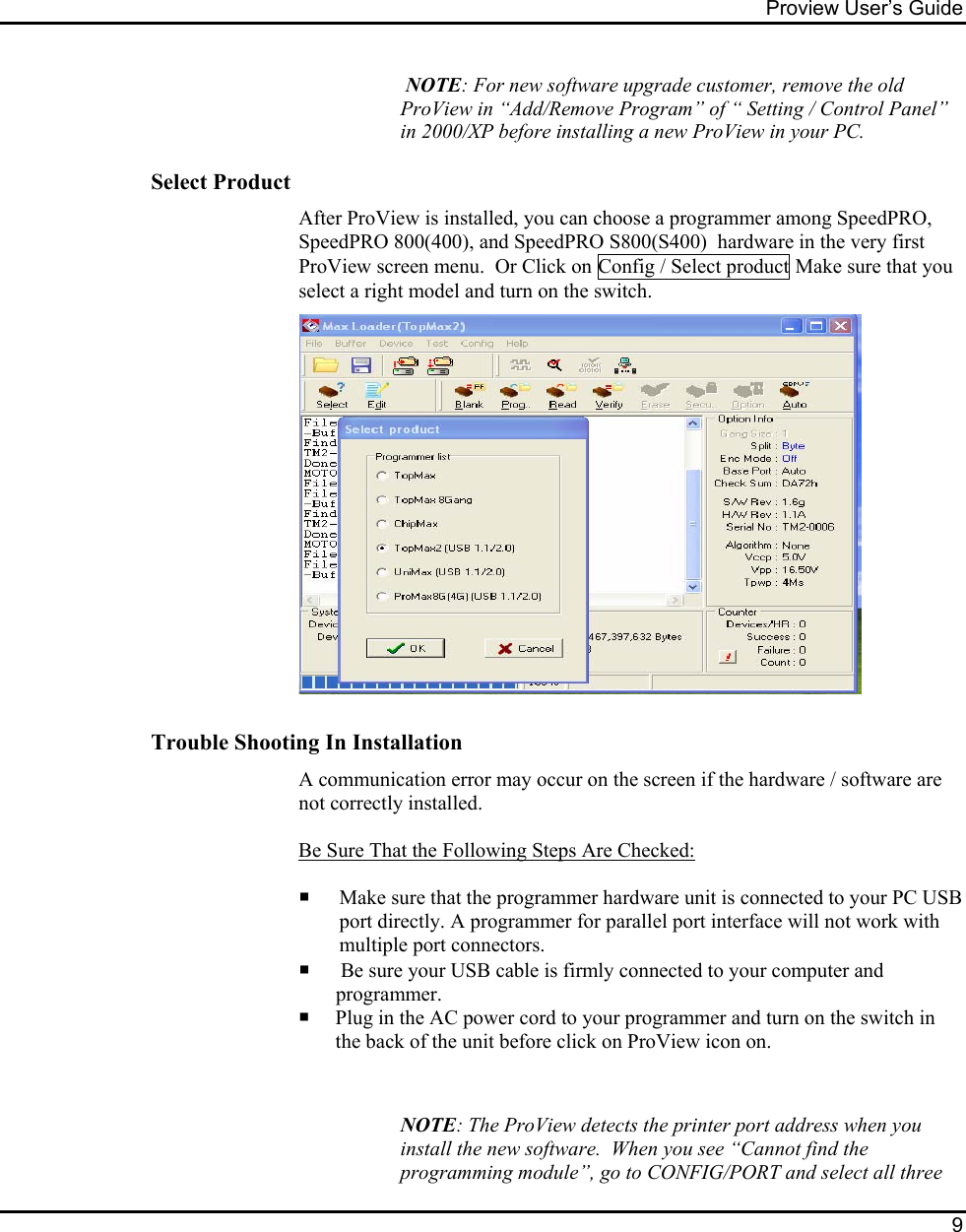
SPEEDPRO User Manual
users manual
Navigation menu
Upload a User Manual
Namespaces
Wiki Guide
HTML
PDF
Info
Views
User Manual
Discussion / Help
Navigation
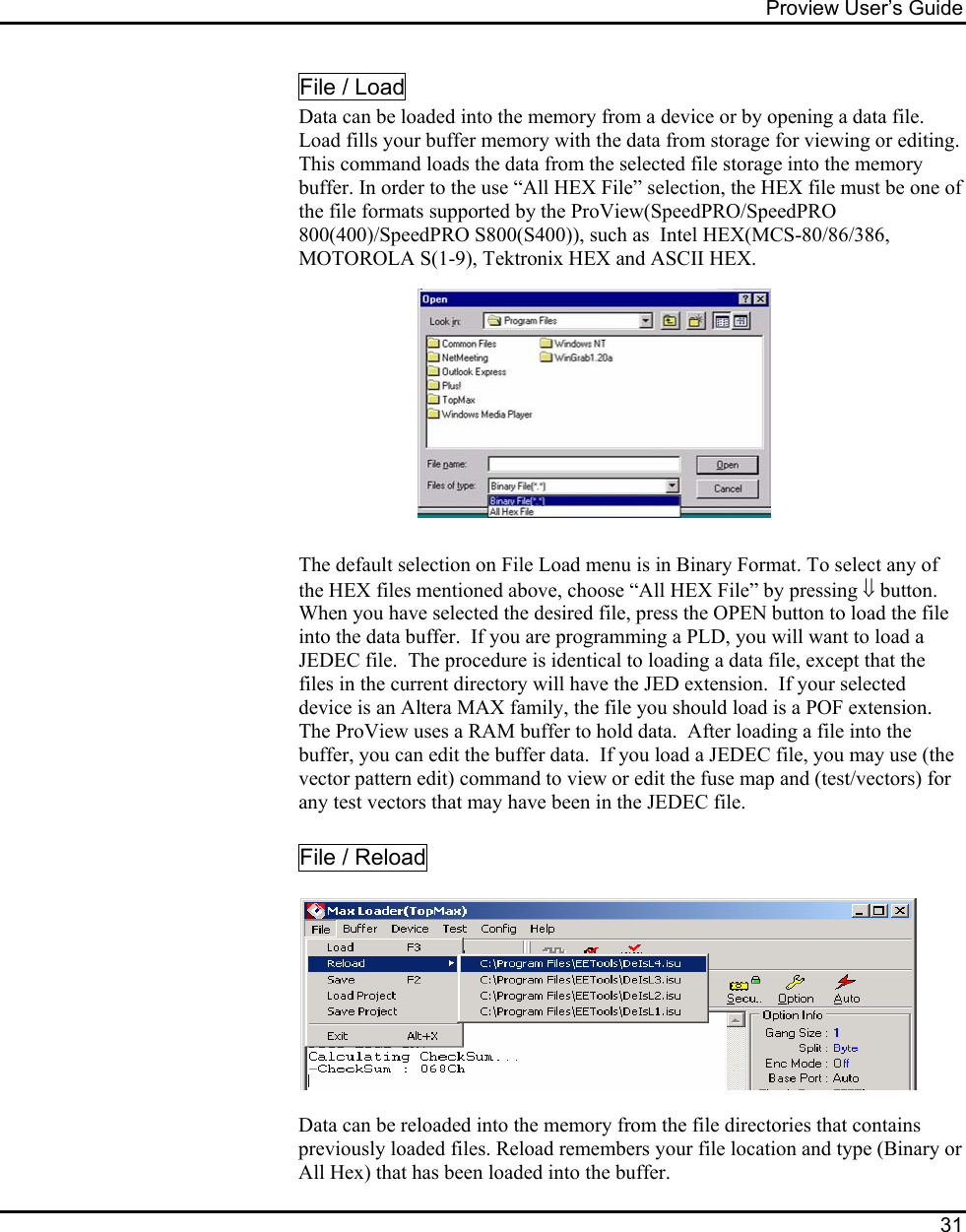
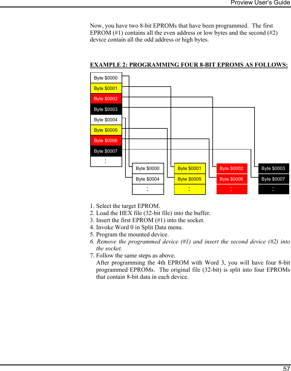
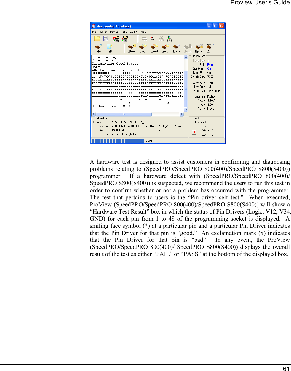
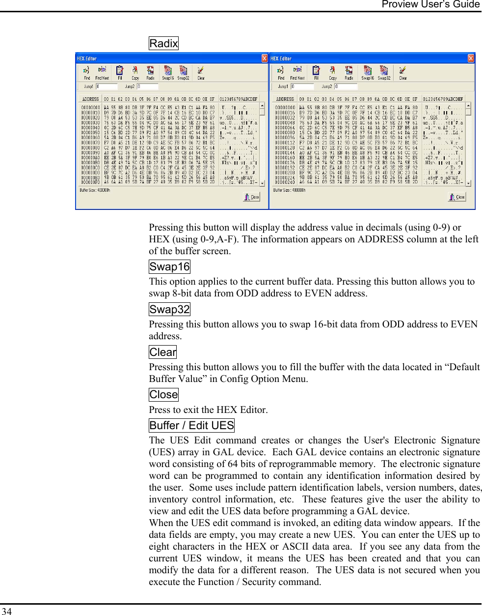
![Proview User’s Guide 32 File / Save Save the current data in your memory buffer to a disk storage by using one of the current supported file formats. Before saving a file, check the buffer and the file address ranges. The contents of the buffer through the specified range will be written into the new file, completely erasing any existing file with the same name. Before saving to a disk, make sure that no file with the same name exists. File/ Load Project A project file that saved by SAVE PROJECT menu is loaded. The project files use the extension (last 3 letters) “.prj.” File/ Save Project This feature allows you to create a job description such as “engineer name” and other useful information for records. It is very useful for future use when you set up all possible environments such as selecting a device, loading a file, and setting other configurations for programming jobs. A job description can be saved as a file name and the same project environment will be ready once you load the same project name. File Name: A file name can be entered with the 3 letter extension “.prj.” Author: An engineer’s name [whom creates this project]. Description: A job explanation that you memorize for your future usage. A device number, File name, and checksum number can be entered in the note pad. Other programming menu descriptions, such as configurations can be described. Buffer Buffer / Edit Buffer This command allows the user to examine and modify the contents of the memory buffer. This section applies to a non-JEDEC file (PROM, EPROM, EEPROM, and Microcontroller) or to a memory chip. If a PLD is being loaded, see the (vector pattern edit) section. The data is presented in HEX and ASCII formats. Find This feature allows you to search the data (ASCII and HEX) in the current](https://usermanual.wiki/Compass-Systems/SPEEDPRO/User-Guide-626435-Page-32.png)
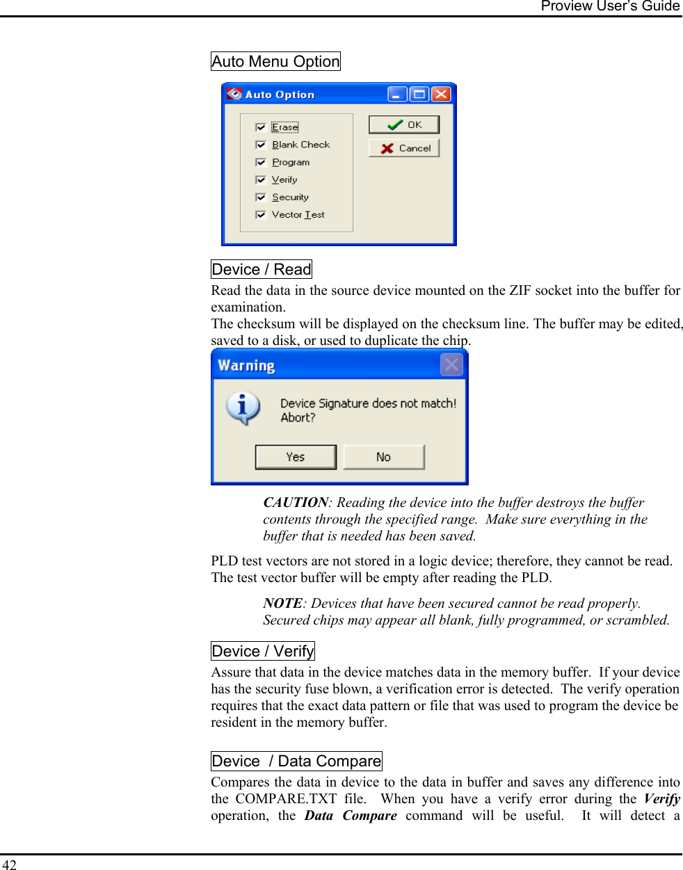
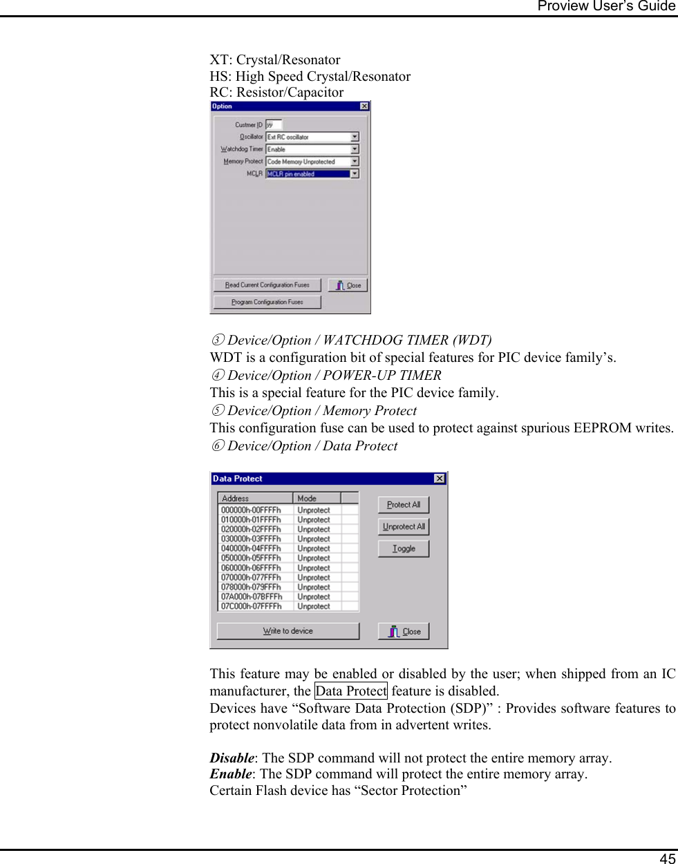
![Proview User’s Guide 40 vector test should be performed (See vector test under the TEST menu). Finally, the part may be secured so that its content can no longer be examined or modified. The security function will not execute if the device fails to verify or pass the vector test properly. 28C256, 28C010, etc. 28CXXX family devices support Software Data Protection. The user has an option of either protecting or not protecting the data. This option must be changed before the start of any programming operation. To change this option, go to the Option selection under DEVICE/FUNCTION menu and make any changes accordingly. To obtain more information about Software Data Protection, please consult the device manufacturer’s specification. Microchip PIC devices Microchip PIC series is different from other Microcontrollers in that they have an EPROM area as well as a CONFIGURATION FUSE. The configuration fuse in the PIC family is used to setup Oscillator Type, Memory Code Protection, Watchdog Timer, or Processor Mode, and etc. After programming the EPROM portion, change the fuses of the items listed under Option. Then you must program the configuration option in the Option menu. Perform the following procedure: 1. Program the main memory 2. Click on the OPTION button 3. Set all of the configuration fuse in OPTION menu 4. Click on the Program configuration fuses button You may also read the status of the Configuration Fuse under the OPTION selection. In order to obtain more information about programming the configuration fuse, contact Microchip technology at +1-602-786-7200 or consult the appropriate data book. Copy from a master chip to a new chip 1. Select the master device from select menu in Microcontroller. 2. Put the chip on the ZIF socket. 3. Click on the Device button and read the chip. 4. Click on the Option button and read the fuses. 5. Write down all of the option fuses [the memory protect must be disabled] in order to copy the information from your master chip. 6. Place a new chip. It must be the same chip as the master chip. 7. The buffer still holds your master data and the memory portion. 8. Click on Option again and set all the fuses that you wrote. 9. (To change the option, use the arrow button in the selection box.) 10. In the same Option menu, Click on the program configuration fuses, read and compare the fuses with your original device.](https://usermanual.wiki/Compass-Systems/SPEEDPRO/User-Guide-626435-Page-40.png)