Compass Systems SPEEDPRO Universal Programmer User Manual Proview Manual
Compass Systems, Inc. Universal Programmer Proview Manual
users manual

Proview User’s Guide
1
ProView
User's Manual
SpeedPRO / SpeedPRO 400(800) / SpeedPRO S400(S800)

Proview User’s Guide
2
1. INTRODUCTION................................................................................................................................................... 6
ABOUT THIS MANUAL ............................................................................................................................................... 6
GENERAL DESCRIPTION ............................................................................................................................................. 6
SELECT PRODUCT ...................................................................................................................................................... 7
BASIC TECHNICAL SPECIFICATION .......................................................... 오류! 책갈피가 정의되어 있지 않습니다.
2. FAMILIES OF DEVICES ................................................................................................................................... 10
EPROM................................................................................................................................................................... 10
EEPROM ................................................................................................ 오류! 책갈피가 정의되어 있지 않습니다.
FLASH MEMORY ................................................................................. 오류! 책갈피가 정의되어 있지 않습니다.
NON-VOLATILE (NV) RAM AND SRAM................................................. 오류! 책갈피가 정의되어 있지 않습니다.
SERIAL EEPROM.................................................................................................................................................... 12
NON-TYPICAL DEVICES........................................................................................................................................... 12
8-bit 1-Megabits.................................................................................................................................................. 12
16-bit 1-Megabits................................................................................................................................................ 13
ERASING AN EPROM .............................................................................................................................................. 13
PLD......................................................................................................................................................................... 13
PLD Features ..................................................................................................................................................... 13
MICROCONTROLLER ................................................................................................................................................ 14
3. TERMS AND SYMBOLS USED IN THE GUIDE............................................................................................ 17
SAFETY NOTE CONVENTIONS .................................................................................................................................. 17
OTHER TERMS AND DEFINITIONS ARE AS FOLLOWS.................................................................................................. 17
CHOOSING THE RIGHT ADAPTER ............................................................................................................................. 19
Different Device Packages.................................................................................................................................. 20
Different Programming Adapters ....................................................................................................................... 21
4. GETTING STARTED / INSTALLATION .......................................................................................................... 7
INSTALLATION REQUIREMENTS ................................................................................................................................. 7
HARDWARE INSTALLATION ....................................................................................................................................... 7
To install the software from the Internet download option ................................................................................ 8
To Install the software from a CD drive.............................................................................................................. 7
TO START THE WINDOWS SOFTWARE ......................................................................................................................... 7
TROUBLE SHOOTING IN INSTALLATION ..................................................................................................................... 9
5. QUICK START EXAMPLES.............................................................................................................................. 22
PROGRAMMING AN EPROM.................................................................................................................................... 22
DUPLICATING AN EPROM....................................................................................................................................... 24
6. OPERATIONS...................................................................................................................................................... 25
BASIC MENU SCREEN INFORMATION ....................................................................................................................... 25
Option Information ............................................................................................................................................ 25
Additional Option Information For Non PLD Devices .................................................................................... 25
System Information............................................................................................................................................ 25
Counter............................................................................................................................................................... 25

Proview User’s Guide
3
File...................................................................................................................................................................... 26
Binary Format ......................................................................................................................................... 27
Intel HEX Format.................................................................................................................................... 27
Motorola S HEX Format......................................................................................................................... 28
TEKTRONIX HEX Format .................................................................................................................... 28
ASCII HEX format ................................................................................................................................. 29
JEDEC Standard <PLD devices only> ................................................................................................... 29
File / Load....................................................................................................................................................... 31
File / Reload ................................................................................................................................................... 31
File / Save ....................................................................................................................................................... 32
File/ Load Project ........................................................................................................................................... 32
File/ Save Project............................................................................................................................................ 32
Buffer ................................................................................................................................................................. 32
Buffer / Edit Buffer......................................................................................................................................... 32
Find................................................................................................................................................................. 32
Find Next ........................................................................................................................................................ 33
Fill .................................................................................................................................................................. 33
Copy ............................................................................................................................................................... 33
Radix .............................................................................................................................................................. 34
Swap16 ........................................................................................................................................................... 34
Swap32 ........................................................................................................................................................... 34
Clear ............................................................................................................................................................... 34
Close ............................................................................................................................................................... 34
Buffer / Edit UES ........................................................................................................................................... 34
Device ................................................................................................................................................................. 35
Select .............................................................................................................................................................. 36
Select / E(E)PROM, FLASH .................................................................................................................. 36
Select / PLD ............................................................................................................................................ 36
Select / Microcontroller .......................................................................................................................... 37
Select / PROM ........................................................................................................................................ 37
Select / Auto Select......................................................................................................................................... 37
Device / Change Algorithm ............................................................................................................................ 37
Device / Blank Check ..................................................................................................................................... 38
Device / Program ............................................................................................................................................ 39
Device / Read ................................................................................................................................................. 42
Device / Verify ............................................................................................................................................... 42
Device / Data Compare.................................................................................................................................. 42
Device / Erase................................................................................................................................................. 43
Device / Security ............................................................................................................................................ 43
Device / Encryption ....................................................................................................................................... 44
Device / Option............................................................................................................................................... 44
○
1 Device/Option /Customer ID.............................................................................................................. 44
○
2 Device/Option / Oscillator ................................................................................................................. 44
○
3 Device/Option / WATCHDOG TIMER (WDT).................................................................................. 45

Proview User’s Guide
4
○
4 Device/Option / POWER-UP TIMER ................................................................................................ 45
○
5 Device/Option / Memory Protect ....................................................................................................... 45
○
6 Device/Option / Data Protect............................................................................................................. 45
○
7 Device/Option / Reset Polarity........................................................................................................... 46
○
9 Device/Option / MCLR....................................................................................................................... 46
○
10 Device/Option / Memory Parity ......................................................................................................... 46
○
11 Device/Option / Low Voltage PGM ................................................................................................... 46
○
12 Device/Option / FLASH Write Enable ............................................................................................... 46
○
13 Device/Option / Background DBG..................................................................................................... 46
○
14 Device/Option / Brownout Voltage .................................................................................................... 46
○
15 Option Item/Read Current Configuration Fuses................................................................................ 46
○
16 Option Item/Program Current Configuration Fuses.......................................................................... 47
○
17 Device/Option/Read Status Byte or Boot Vector................................................................................ 47
○
18 Device/Option/Program Status Byte or Boot Vector.......................................................................... 47
○
19 Device/Option/Initialize Device ......................................................................................................... 47
Device / Auto.................................................................................................................................................. 47
Test ( These functions are only for TopMax )............................................................................... 48
Test / Vector Test ........................................................................................................................................... 48
Test / IC Test .................................................................................................................................................. 49
Test / RAM Test ............................................................................................................................................. 49
Config ................................................................................................................................................................. 50
Config / Select Product................................................................................................................................... 50
Config Option ................................................................................................................................................. 51
Config Option / Default Buffer Value ................................................................................................... 55
Config Option / Buffer Clear Before File Loading............................................................................... 51
Config Option / Blank Check Before Programming............................................................................. 52
Config Option / Verify After Reading.................................................................................................... 52
Config Option / verify after programming ............................................................................................ 52
Config Option / Byte order swapping .................................................................................................... 52
Config Option / Device Insert Test ........................................................................................................ 54
Config Option / Auto Repeat Programming..........................오류! 책갈피가 정의되어 있지 않습니다.
(Under development) ..............................................................오류! 책갈피가 정의되어 있지 않습니다.
Config Option / Port .......................................................................오류! 책갈피가 정의되어 있지 않습니다.
Config Option / Gang Split Select .................................................................................................................. 55
Gang ...................................................................................................................................................... 55
Split ........................................................................................................................................................ 56
Config Option / Address ................................................................................................................................. 58
File Load................................................................................................................................................ 59
File Save ............................................................................................................................................... 59
Config Option / Auto Inc................................................................................................................................ 60
Config / Hardware test.................................................................................................................................... 60
7. TROUBLE SHOOTING & TECHNICAL SUPPORT ..................................................................................... 62

Proview User’s Guide
5
1. REGISTRATION ..................................................................................................................................................... 62
2. SOFTWARE UPDATES ........................................................................................................................................... 62
3. TESTING THE HARDWARE .................................................................................................................................... 62
4. QUICK SELF-DIAGNOSTICS .................................................................................................................................. 62
5. CALLING CUSTOMER SUPPORT ............................................................................................................................ 63
6. SERVICE INFORMATION........................................................................................................................................ 64
7. LIMITED ONE-YEAR WARRANTY......................................................................................................................... 65
8. USEFUL WEB SITE ADDRESSES/ PHONE NUMBERS .............................................................................................. 65
9. PROGRAMMING ADAPTER MANUFACTURERS ...................................................................................................... 66
10. EPROM EMULATOR MANUFACTURERS ............................................................................................................ 66
8. GLOSSARY .......................................................................................................................................................... 66

Proview User’s Guide
6
1. INTRODUCTION
This manual describes the operation of Compass Systems’
SpeedPRO/SpeedPRO 800(400)/SpeedPRO S800(S400) software, Proview,
driven device programmer. The information contained in this manual has been
reviewed for accuracy, clarity, and completeness.
Please report in writing any errors or suggestions to info@compass21.com
Compass Systems, Inc.
1403 ACE Techno Tower 8, 191-7, Kuro-Dong, Kuro-Gu
Seoul, Korea.
www.Compass21.com
Tel : +82-2-2109-8660
Fax : +82-2-2109-8661
Compass Systems reserves the right to use and distribute any information
supplied without obligation.
About This Manual
SpeedPRO/SpeedPRO 800(400)/SpeedPRO S800(S400) software, Proview User
Guide explains how to install and run the programming software on your
computer.
Chapter 2 contains instructions for installing and running ProView.
Chapter 3 describes the most popular programmable devices.
Chapter 4 contains all terms and symbols used in the manual.
Chapter 5 describes basic operating examples of programmers.
Chapter 6 is organized by main operating commands and gives detailed
instructions on each command.
Chapter 7 provides troubleshooting information for identifying and solving
problems with programmers. It provides a detailed guide for Compass
Systems’ technical support and return material procedures.
Chapter 8 introduces an useful product, EPROM Emulator.
Chapter 9 contains useful glossary about programmable devices and
package types.
This Manual assumes that you have a working knowledge of your personal
computer and its operating conventions.
General Description
SpeedPRO/SpeedPRO 800(400)/SpeedPRO S800(S400) are software driven
device programmers that support a wide variety of programmable devices
including: EPROM, EEPROM, Serial PROM, EPLD, PEEL, GAL, FPGA, and
single chip Microcontroller.

Proview User’s Guide
7
SpeedPRO/SpeedPRO 800(400)/SpeedPRO S800(S400) connects to the
USB(1.1 or 2.0) port of any IBM PC, and can operate with a full spectrum of
IBM compatibles.
The great advantage of programmer is their programming speed and
superior software. All programmers are controlled via a host IBM PC computer.
The operating software has a user-friendly interface that includes window pull-
down menus and virtual memory management to deal with very large files.
2. GETTING STARTED / INSTALLATION
Installation Requirements
ProView is designed to operate with any 386, 486, Pentium, PS/2, Portable
(notebook), compatibles running WIN 95/98/ ME/NT/2000, and XP. The
computer requires a CD-ROM drive, but a hard disk drive is also recommended
Hardware Installation
The following section details the procedure for accomplishing the hardware
installation procedure. SpeedPRO/SpeedPRO 800(400)/SpeedPRO S800(S400)
connects to USB 1.1 or 2.0 port in your PC.
To Install the software from a CD drive
Place CD in the CD drive.
Choose Device Programmer from the list of files located on the CD.
And then The SETUP program will launch the installation procedure.
To Start the windows software
To run the windows software, select your product model shortcut in the
Windows Start Menu / Programs list.
From Configuration Menu, you can choose one of the SpeedPRO/
SpeedPRO 800(400)/SpeedPRO S800(S400) that you use.
To installation the software for USB programmers
1. Install a programmer software that comes in Compass Systems CD
(Download the latest software (all-in-one) from www.compass21.com )
2. Run the ProView in a directory (default destination C:\Compass)
3. Turn the AC switch is ON or connect power cord to programmer and connect
an USB cable between PC and programmer. Do this step same numbers as
programmers.
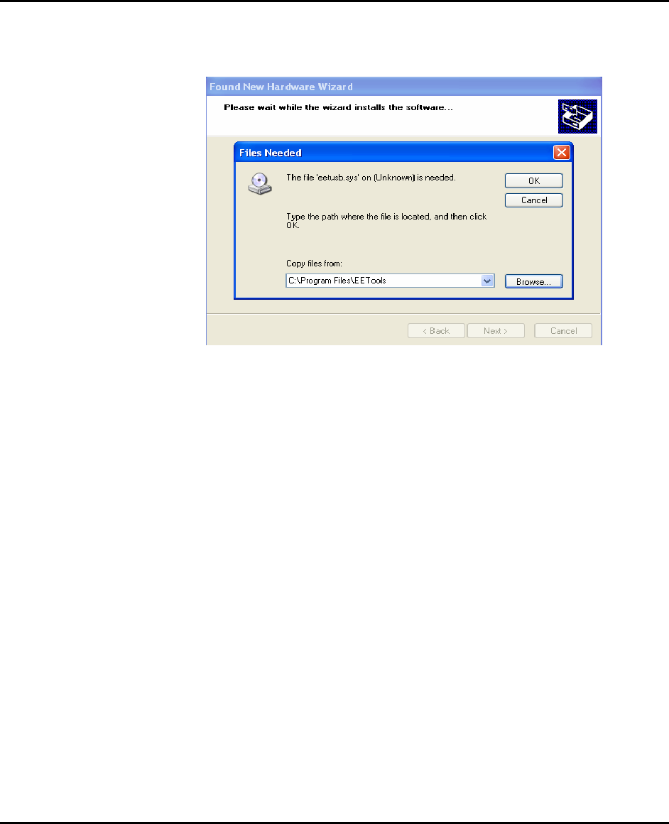
4. For USB driver installation, you may choose “specific location” when the
“Found New Hardware Wizard” appears during the set up wizard.
The default programmer’s USB driver is located in
C:/Compass/Proview directory.
Proview User’s Guide
8
(driver’s name: proview.inf, proview.sys )
To install the Software for parallel port programmers
There are three different addresses for the parallel port. When you select an
address from LPT1, LPT2, LPT3, one of them should be valid without a
communication error message. Turn the AC switch ON before running the
ProView software. Make sure that you connect USB cable between SpeedPRO/
SpeedPRO 800(400)/ SpeedPRO S800(S400) and your available printer port and
lock the shields in each side of the cable. Be sure that your programmer
recognizes your computer’s parallel port address when you execute the ProView
icon. (DEMO mode is indicated that your programmer has a “communication
error”)
1. Connect USB cable between PC and programmer.
2. Connect AC cord to programmer.
3. Turn on AC switch located in back side of SpeedPRO
4. Install a programmer software that comes in a CD-R ( or download the latest
software (all-in-one) from www.compass21.com
5. After the ProView is installed, you choose SpeedPRO hardware in the very
first screen menu
To install the software from the www.compass21.com web site
1. Click on Software download on www.compass21.com and download
ProView software and the file will be saved in your hard disk. The ProView can
be operated for All-in-one (all programmers-in-one software).
2. Once the download is complete, double-click on the file name to install the
software.
Proview User’s Guide
9
NOTE: For new software upgrade customer, remove the old
ProView in “Add/Remove Program” of “ Setting / Control Panel”
in 2000/XP before installing a new ProView in your PC.
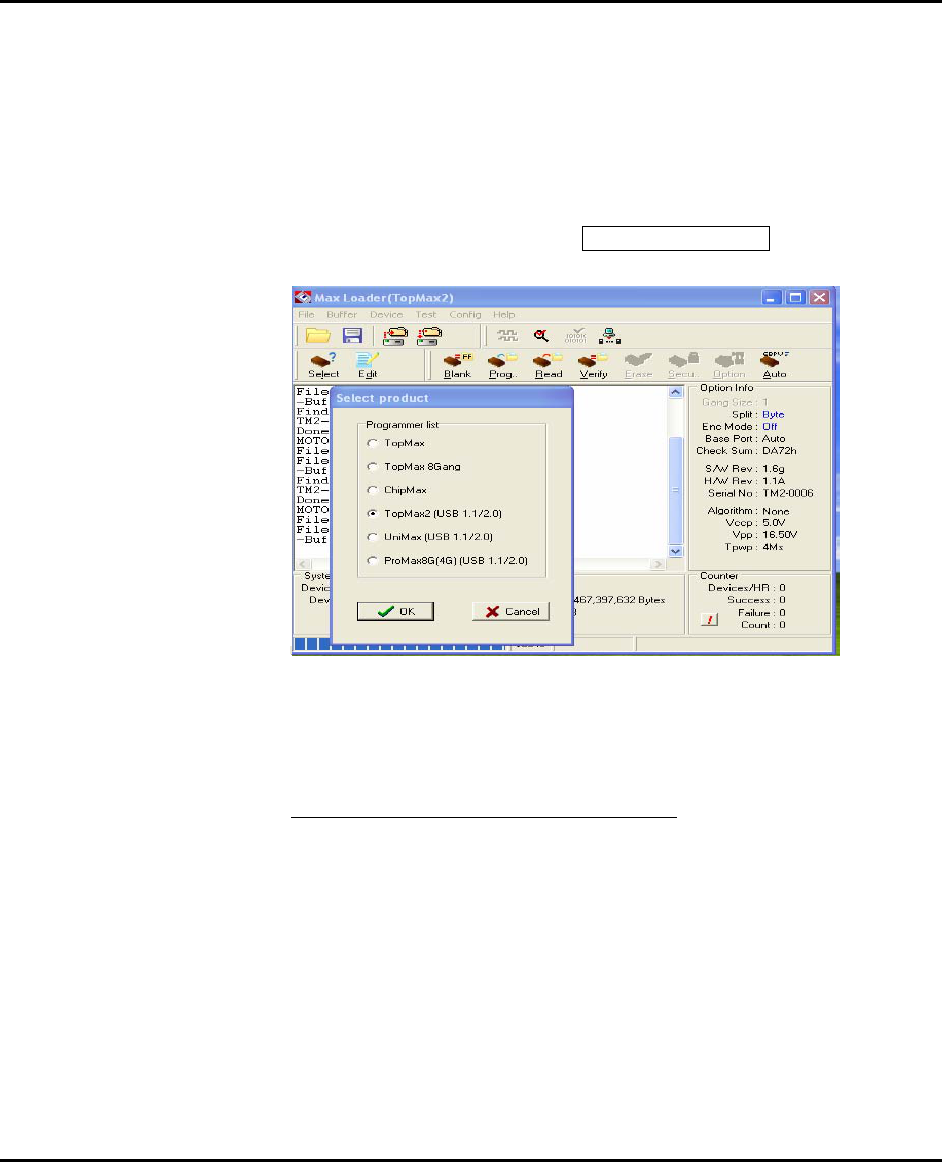
Select Product
After ProView is installed, you can choose a programmer among SpeedPRO,
SpeedPRO 800(400), and SpeedPRO S800(S400) hardware in the very first
ProView screen menu. Or Click on Config / Select product Make sure that you
select a right model and turn on the switch.
Trouble Shooting In Installation
A communication error may occur on the screen if the hardware / software are
not correctly installed.
Be Sure That the Following Steps Are Checked:
Make sure that the programmer hardware unit is connected to your PC USB
port directly. A programmer for parallel port interface will not work with
multiple port connectors.
Be sure your USB cable is firmly connected to your computer and
programmer.
Plug in the AC power cord to your programmer and turn on the switch in
the back of the unit before click on ProView icon on.
NOTE: The ProView detects the printer port address when you
install the new software. When you see “Cannot find the
programming module”, go to CONFIG/PORT and select all three
Proview User’s Guide
10
parallel port addresses. If you see the same error message
continuously, you should contact technical support.
3. FAMILIES OF PROGRAMMABLE DEVICES
The devices that are supported on the Compass Systems, Inc programmers are:
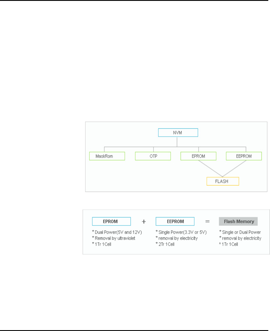
NVM : Non Volatile Memory
ROM : Read Only Memory
OTP : One Time Programmable ROM
EPROM : Erasable Programmable ROM
EEPROM : Electrically Erasable & Programmable ROM
NVM Hierarchy
Flash Memory
Proview User’s Guide
11
Flash Memory Technologies
A B C(and) C(nand) A B C(or) C(nor)
0 0 0 1 0 0 0 1
0 1 0 1 0 1 1 0
1 0 0 1 1 0 1 0
1 1 1 0 1 1 1 0
Performance Comparison
* NAND Flash : High Wright Performance
Proview User’s Guide
12
Serial Flash EEPROM
The non-volatile Serial Flash Memory is widely used for code storage and user
settings in cost-sensitive applications such as CD and DVD players, set-top-
boxes (STB), digital-TV and cameras, graphic cards, printers, PC motherboards
and flat panel displays. These products typically run their operating code from
fast Random Access Memory (RAM), after downloading the code from the low-
cost Serial Flash Memory at power-up. Several semiconductor manufacturers
produce this device family named as 25xxx.
Serial EEPROM
These devices are electrically erasable, but they operate in a series rather than in
parallel.
Xilinx 17xx family
From the Xilinx 17xx series, the RESET Polarity can be changed only on
Xilinx 17xxD/L and 17128. On devices with EPROM portion already
programmed or on new blank devices, RESET polarity is HIGH.
The current status of the Reset pin polarity is determined and displayed on
the screen after Reading the device. The polarity of the Reset pin can
ONLY be changed from HIGH to LOW, but not vice versa. To change the
polarity, click on the Option button and check on the Reset bit box before
programming your device. To make certain that the RESET Polarity has
been changed, read the device again. On other serial EEPROM devices (but
NOT Xilinx 17xxD/L & 17128) the RESET polarity is always HIGH and it
cannot be changed to LOW.
Non-Typical Devices
8-bit 1-Megabits
There are four types of 1 Megabits EPROMS. One set has the A16 and OE lines
swapped. However, these devices will still program and verify like normal 1
Megabits. Once these devices are placed into the circuit, it will appear as if they
have not been programmed correctly. This is not due to the ProView software
or the programmer, but the difference between these 1 Megabits. When selecting
a 1 Megabit, it is important to determine which one you have. Here is a list of 1
Megabits and their equivalents:
27010 (normal pin-out -- program as GENERIC or INTEL 27010):

Proview User’s Guide
13
Equivalents: INTEL 27010, HITACHI 27101, TOSHIBA 571000, NEC
271001, MITSUBISHI 27101
27301 (non-standard pin-out -- program as HITACHI 27301's):
Equivalents: HITACHI 27301, NEC 271000, MITSUBISHI 27100,
TOSHIBA 571001, INTEL 27C100
16-bit 1-Megabits
Any devices with the number 27210, 271024 and the MITSUBISHI 27102.
27011: The 27011 is a 28-pin 1-megabit device that is organized into 8 pages of
16k-bytes. NOTE: The 27513 is 4 pages of 16k-bytes.
Erasing an EPROM
An EPROM has a quartz window located on the chip just above the die. Erasing
an EPROM is done by exposing the EPROM to high-frequency ultra-violet(UV)
light waves. Erasing an EPROM usually takes from 15-20 minutes, but may be
shorter or longer, depending on the device. Many manufacturers make EPROM
erasers. If you wish to purchase an eraser, call. Compass Systems at +82-2109-
8660. When an EPROM is not being erased, the window may be covered with
an opaque label. Sometimes (over a period of years) an EPROM will start to
erase due to the rooms level of fluorescent light. Direct exposure to sunlight
also has this effect, but happens much more rapidly.
PLD
A programmable logic device (PLD) consists of an array of logic gates and flip-
flops that can be programmed to implement an almost unlimited number of logic
designs. These are programmable logic arrays that can be EEPROM based,
EPROM based, fused link, anti-fuse, or Flash-based technology. They are
programmable by the user to implement logic circuits in order to reduce part
count and turnaround time. PLDs are programmed according to a fuse map,
which is typically contained in a JEDEC file.
PLD Features
Many different PLDs are available from the IC manufacturers. PLDs are
fabricated using either bipolar or CMOS Processes. All PLDs are made up of
combinations of AND gates, OR gates, inverters, and flip-flops.
PAL: The PAL is a PLD with a fuse-programmable AND array. The
PAL’s AND gates connect to OR gates in a fixed pattern.
PROM: For many years, the PROM was not classified as a PLD, even
though most of the smaller PROMs (32 x 8 organization, for example)
were being used as logic elements. The larger PROMs were still
applied in bipolar microprocessor designs to store microcode
instructions. The PROM has an architecture similar to the PAL, except
that the PROM’s AND array is fixed while its OR array is
programmable.
FPLA: The field-programmable logic array (FPLA) consists of a
programmable AND array like the PAL, with a programmable OR
array like the PROM. The FPLA is therefore a more general PLD

Proview User’s Guide
14
because any product term may be connected to any output OR gate.
Because the entire IC is programmable, the FPLA can implement some
functions which a PAL or PROM may not be able to implement.
EPLD: Several manufacturers produce PLDs which can be erased and
reprogrammed like EPROMs. These ICs are called erasable
programmable logic devices, or EPLDs. Internally, they have the same
programmable AND-OR-register structures of the PAL and FPLA.
Microcontroller
These devices are CPU's with on-chip EPROM and RAM. They are typically 40
pins and are UV erasable. They have part numbers such as Intel's
8748,8749,8751,8752 etc. A micro-controller is generally a computer-on-a-chip
with RAM, ROM, and I/O ports. Microcontrollers are usually used for specific
purposes, such as keyboard decoders, printers, clocks, telephones, CD-players,
or any other application that requires a small, on-board computer.
Microcontrollers are used to take the place of in-circuit logic, as it can be less
expensive and take less space. Also, since it is software driven, the device may
be updated very easily. Micro-controllers have the ability to use internal as well
as external RAM. Also, micro-controller data may be encrypted or otherwise
secured to prevent copying of the data or program information. Microcontrollers
also have their own instruction set, usually very similar to familiar microproce-
ssors (such as the 8080 or 8086). The INTEL MCS-51 family features up to 64k
each of internal and external memory, 32 I/O lines, interrupts, timers, and bit-
addressable RAM. Its instruction set contains 111 instructions. However, for
specific purposes, limited versions of the 51 family are available. For instance,
the Signetics 87c751/87c752 families do not allow external RAM to be used,
and have limited I/O channels, etc. However, these devices still allow for
data/program encryption and security levels. They are also less expensive than
the MCS-51 micro-controllers.
See the help selection under MAIN-MENU COMMANDS for Encryption and
Security-bit information.
NOTE: Programming Microchip PIC family
Microchip PIC series are different from other Microcontrollers in that
they have an EPROM area as well as a Configuration Fuse. The
Configuration Fuse in the PIC family is used to setup different
Oscillator types, to set Memory Code Protection and Watchdog timer,
and etc. To program this fuse:
1. Program the EPROM portion of the device
2. Click on Option
3. Make any changes if necessary
4. Click on the Program Configuration Fuses button to program
the fuse information that you want to program
5. Click on the Read Current Configuration Fuses button to read
back the current status of the fuse
Proview User’s Guide
15
6. Press the Close button
NOTE: In order to obtain more information about programming the
configuration fuse, please contact Microchip technology at 602-786-
7200(USA) or refer to their data book.
About “Device ID” and “Auto Select” on EE Tools programmers
Most of devices have own manufacturer and device ID in each programmable
devices such as E(E)PROM / Flash Memory, PLD, and MCU.
However old type of device such as PAL, PROM doesn’t have ID because IC
makers didn’t put its ID for old type chips.
(Auto Select)
As you can see the “warning” in the Auto Select menu in ProView, we can only
guarantee the “auto select” function for 32-pin or less device in E(E)PROM /
Flash Memory. Since device library in programmer software has information for
these standard devices, users can utilize this feature as their purpose. However,
all other devices such as PLD, Serial Memory, Microcontroller, and FPGA are
not able to be recognized by programmer software automatically. We use this
feature as optional device selection menu. Auto Select command allows you
choose an unknown device through device IDs which were recorded in ProView
library. Put a device up to 32-pin on the ZIF socket of programmer and click on
“Auto Select” in Select Device menu. It will find out a correct device ID and
choose a correct device for you.
Proview User’s Guide
16
(To Find a Device ID)
After selecting a certain device from Select Device menu and plug-in a
corresponding device in ZIF socket, you can see the ID(s) when you pressing
“shift” and “f1” keys in your keyboard.
In software menu, Chip(in socket) MFG(manufacturer) ID and DATA(in
software) ID must be same if your device is valid .
If not, check the socket with your device if you use NON-Standard(DIP) device
or use test other devices in case the first device may be defective. This ID check
must be passed before further operation on your device.

Proview User’s Guide
17
4. TERMS AND SYMBOLS USED IN THE GUIDE
Safety Note Conventions
NOTE assists the user in performing a task. It makes the job more easily
understood.
CAUTION alerts the user that unexpected results or damages to a device
may occur if an instruction is not followed.
Other terms and definitions are as follows
Toolbar : Clicking on a toolbar button manipulates operations or
commands for ProView(SpeedPRO 800(400)/SpeedPRO
S800(S400)) programmer software.
Bold/Italics : actions items/software functions, i.e. Edit Button, IC Test,
or Change Algorithm.
Device : The IC you are attempting to read, program, or verify.
Buffer : The work area in your computer memory to execute Read,
Save, Program, and Verify. The Buffer size may be from
64K to 32 Megabytes.
NOTE: If the size of a device is bigger than the buffer size in
your computer, ProView will use the hard disk space
(swapping). For this reason, the ProView software can handle
devices up to unlimited size of E(E)PROMs with your standard
memory space ( a minimum of 512KB RAM memory is
required).
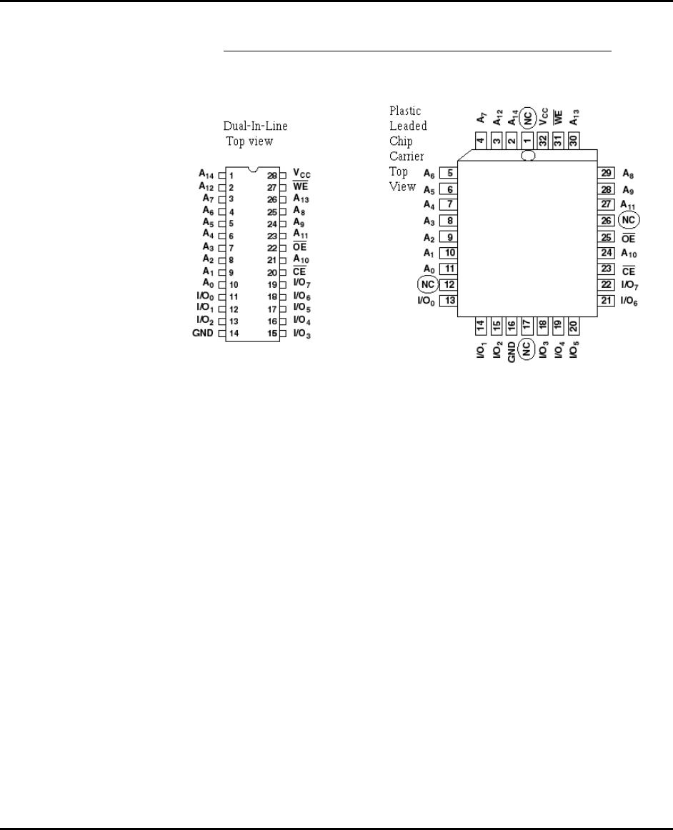
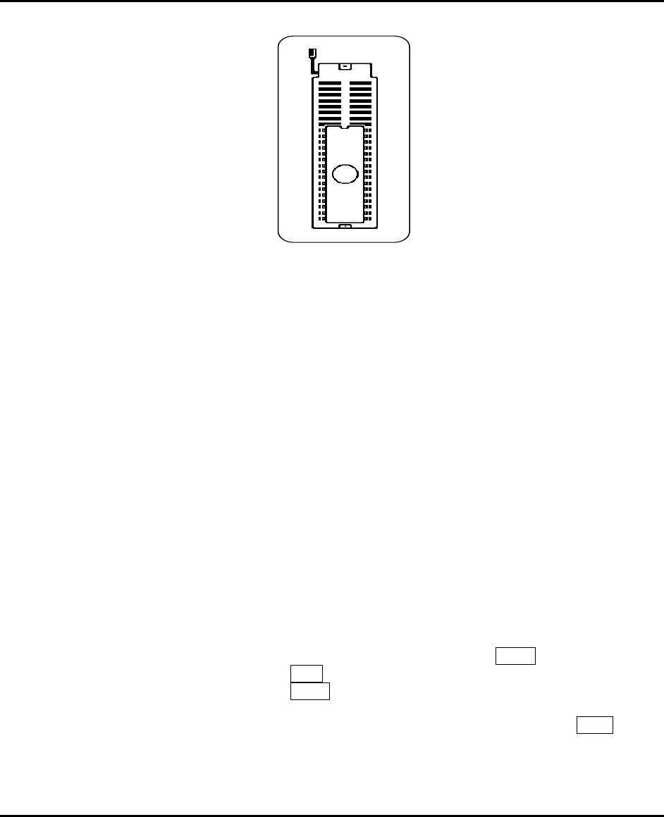
Inserting a DIP Device
Pin 1 on a DIP package is generally indicated by a notch on one end of the
device. Pin 1 is also indicated by a stamped or recessed dot on one corner of the
device. In the illustration below, the notch and the dot are highlighted by arrows.
The dot is on the left and the notch is on the right.
To Insert a DIP device into the ZIF socket:
CAUTION: Devices are static sensitive. Operate your programmer at
an antistatic workstation. To avoid electric shock and damage to the

Proview User’s Guide
18
devices, use an antistatic wrist strap containing a 1 mega-ohm
(minimum) to 10 mega-ohm (maximum) isolating resistor.
1. Lift the socket lever to the open position.
2. With the notched end facing the top of the socket, place the device in
the socket so that the bottom of the device is aligned with the bottom
of the socket (bottom justified).
3. Lower the socket lever to lock the device into the socket.
4. When you are done, select the device you just inserted.
Inserting a PLCC Device
NOTE: In order to use PLCC devices, your programmer must have a
proper adapter for the device. Consult your programmer's adapter list
for the non-standard device.
Pin 1 on a PLCC package is generally indicated by a notch on one corner of the
device. Pin 1 is also indicated by a stamped or recessed dot on one side of the
device. In the illustration below, the notched corner and the dot are highlighted
by arrows. The notch is on the left and the dot is on the right.
To Insert a PLCC device into an adapter:
CAUTION: Devices are static sensitive. Operate your programmer at
an antistatic workstation. To avoid electric shock and damage to the
devices, use an antistatic wrist strap containing a 1 mega-ohm
minimum) to 10 mega-ohm (maximum) isolating resistors.
1. Open the adapter 90 degrees, set its front edge under the two tabs at the front
of the base opening, and lower its back edge into place.
2. Orient the device you want to use so that pin 1 is next to the retaining latch.
Each Adapter has a small molded dot that represents pin 1 and a notched
corner that can be used to align chamfered corners of devices.
3. Insert the device into the open adapter.
4. Close the Adapter, and press the retaining latch forward with your thumb until
the latch snaps into place.
5. If you have not already, select the device you just inserted
Proview User’s Guide
19
Pin Connection Diagram Example between DIP and PLCC package
Choosing the Right Adapter
Most programming adapters are simple package converters. They allow TSOP,
QFP, SOIC, or PLCC devices to plug into the same device’s DIP footprint.
These adapters are available for memory, logic and Microcontrollers. They can
often be used with many devices from various manufacturers. For devices that
cannot use a generic footprint we have offered adapters to work with specific
programmers.
Here is what you need to know to select the appropriate adapter.
1) The part number and manufacturer of your device.
2) The device package. (TSOP, PLCC, DIP, QFP, SOIC, etc.)
(Refer to the following package drawings)
3) Your device pin count.
4) In some cases you will need your device package dimensions for SOIC,
SSOP, and TSOP chips.
Proview User’s Guide
20
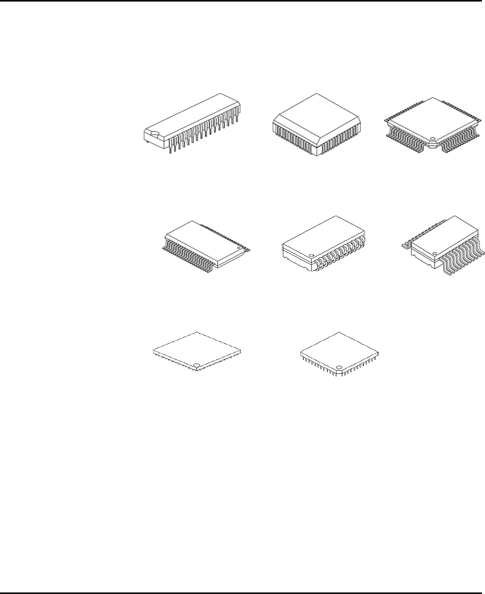
Different Device Packages
DIP PLCC QFP
TSOP SOJ SOIC
BGA PGA
Proview User’s Guide
21
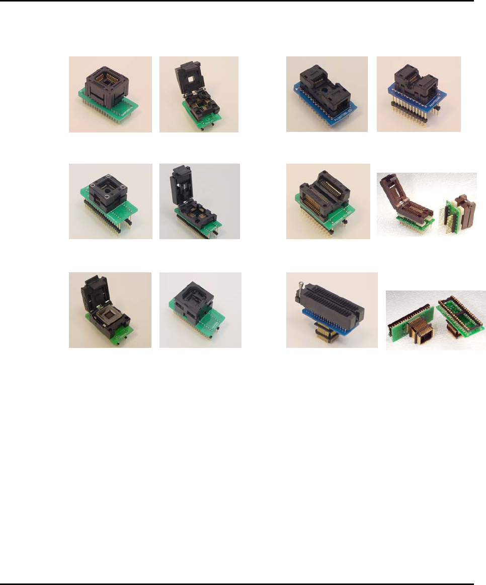
Different Programming Adapters
PLCC-TO-DIP TSOP-TO-DIP
QFP-T
QFP-TO-DIP SOIC-TO-PLCC
BGA-TO-DIP DIP-TO-PLCC (for Emulator)
Useful Glossary for IC packages
-BGA: Ball Grid Array
-BQFP: Bumpered Quad Flat Pack
-CBGA: Ceramic Ball Grid Array
-CFP: Ceramic Flat Pack
-CPGA: Ceramic Pin Grid Array
-CQFP: Ceramic Quad Flat Pack
-TBD: Ceramic Lead-Less Chip Carrier;
-DLCC: Dual Lead-Less Chip Carrier (Ceramic);
-FBGA: Fine-pitch Ball Grid Array
-fpBGA: Fine Pitch Ball Grid Array
-JLCC: J-Leaded Chip Carrier (Ceramic);
-LCC: Leaded Chip Carrier
-LCCC: Leaded Ceramic Chip Carrier;

Proview User’s Guide
22
-LFBGA: Low-Profile, Fine-Pitch Ball Grid Array;
-PLCC: Plastic Leaded Chip Carrier
-PQFD: Plastic Quad Flat Pack
-PQFP: Plastic Quad Flat Pack
-PSOP: Plastic Small-Outline Package
-QSOP: Quarter Size Outline Package
-SOIC: Small Outline IC;
-SSOP: Shrink Small-Outline Package
-TQFP: Thin Quad Flat Pack;
-TSOP: Thin Small-Outline Package
-TSSOP: Thin Shrink Small-Outline Package
-TVSOP: Thin Very Small-Outline Package
-VQFB: Very-thin Quad Flat Pack
-CERDIP: Ceramic DIP
-DIP: Dual In-line Package
-TBD: Dual In-line Zig-Zag Package;
-HDIP: Hermetic DIP
-PDIP: Plastic DIP
-PGA: Pin Grid Array;
-SIP: Single In-line Package
5. QUICK START EXAMPLES
If you are using a programmer for the first time, this section will help you to
become familiar with the basic operating procedure. This section includes two
examples of device programming with your programmer.
Programming an EPROM with data
We selected an AMD 27C010 EPROM to show you how to program an
EPROM. The 27C010 EPROM needs to be erased (blank) before this procedure
begins.
NOTE: EPROMs have a quartz window that can be erased by exposing
the EPROMs to Ultra-Violet(UV) light. Erasing an EPROM usually
takes 10-30 minutes.
1. Click on the ProView icon in your Desk top menu after installing the
ProView in your PC.
2. Check the optional configuration before programming begins.
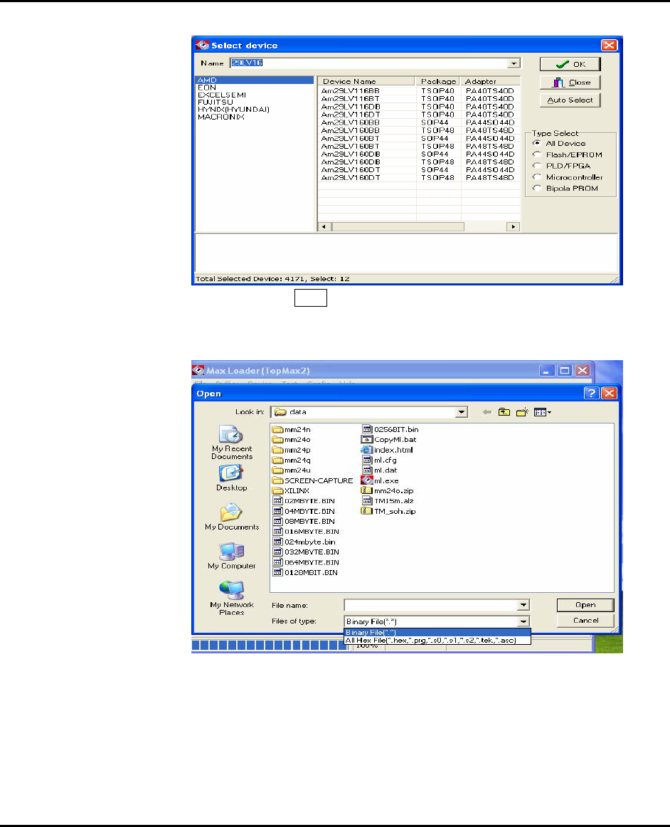
3. Click on the Select button. There are two different ways to select the target
device from the menu: by choosing the device manufacturer and type using
the arrow keys or you may type the manufacturer and the device names on
NAME box. ProView will display the names of devices that have the best
match to your input. After selecting the device, the detailed device
information box is provided below the select menu screen.
Proview User’s Guide
23
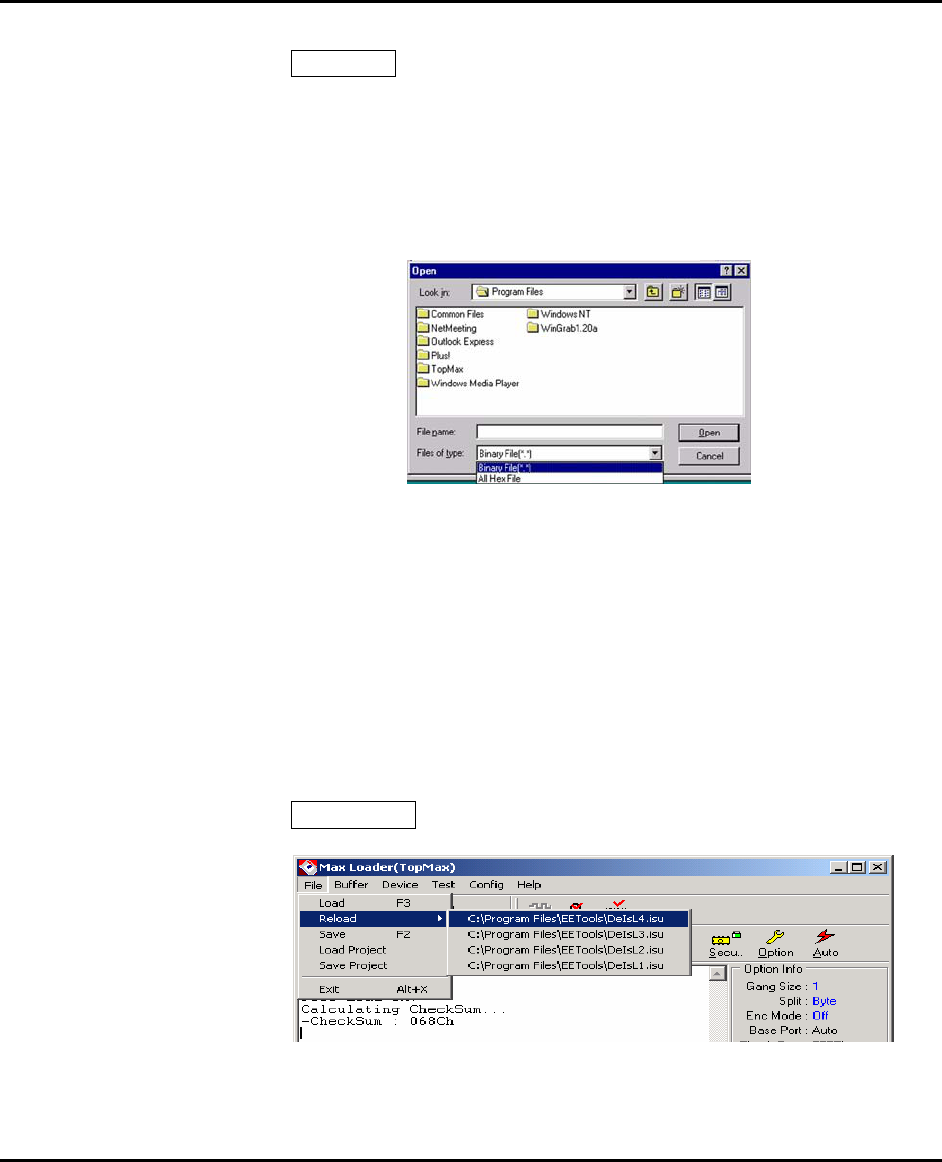
4. Click on the Load to load a file from a floppy or hard disk into the buffer.
Change your file directory by choosing a directory in Look in box. Choose a
file name and type of the file. Make sure that the file type is selected; ”All
Hex File” or “Binary file” is located in the File of type box.
5. Insert the 27C010 device into the ZIF socket. After inserting the part, make
sure that the socket handle is down (close) to secure the chip.
See the illustration below:
Proview User’s Guide
24
6. Click on the highlighted cursor Blank Check.
NOTE: If an EPROM is not erased completely, it will not pass the
Blank Check. If an EPROM is damaged to begin with, it may not pass
the blank check, although it has been erased for a long time in UV
eraser.
7. Click on the Program.
CAUTION: Do not touch the device while the BUSY green LED light is
on (programming is in progress).
After programming a device, the part is automatically verified. The Checksum
is calculated and displayed in the OPTION info. In order to verify your work,
read the programmed part again. If this Checksum value matches to that of the
programming checksum, then the 27C010 is programmed successfully.
Duplicating an EPROM
The following is an instruction on duplicating a programmed device. In order to
do so a source device and an erased (blank) target device are necessary.
Source Device: Programmed AMD 27C256
Target Device: Erased or blank INTEL 27C256
1. Make sure the ProView is displayed without any communication error (refer
to programming section ).
2. Place the AMD 27C256 device into the ZIF socket.
3. Select the manufacturer and part names from the Select menu.
4. Click on the Read button. In order to make sure the device is read properly,
Click on the Verify button.
5. Remove the current chip from the socket and replace it with the erased or
blank Intel 27C256 device. Select the appropriate device from Select menu
on screen.
NOTE: You do not need to change the device information if you use the exact
same chip as the source device.

Proview User’s Guide
25
6. Click on the Blank button.
7. Click on the Program button. The part will be programmed and verified
automatically. If no error messages appear during the Programming or
Verification process, your duplicating work is done successfully. You have a
duplicated Intel 27C256 part from AMD 27C256 chip.
6. PROVIEW OPERATIONS
This section describes the operation of the software. The Main standard system-
menu is divided into four display areas: Main operation menu screen, Option
Information, System information, and counter.
Basic Menu Screen Information
Option Information
• Gang Size : Current socket size when ProView is used
• Split : Current world format for split programming
• Enc Mode : Enable or Disable Encryption mode for
Microcontrollers
• Base Port : Current parallel port address
• Check-Sum : Check-Sum number of the data in current buffer
• H/W Rev : Hardware revision number for your programmer
• S/W Rev : Current ProView software revision number
• Serial No : Serial number of ProView hardware
(Additional Option Information For Non PLD Devices)
The following information presents programming information of the selected
device.
• Algorithm : Programming Algorithm
• Vccp : Main Power Supply Voltage
• Vpp : Programming Power Supply Voltage
• Tpwp : Programming Pulse Width
System Information
• Device Name : The current device number with manufacturer name
• Device Size : The size of device in HEX value
(Ending Address –Starting Address + 1)
• Free Disk : Check the free disk space for a big size E(E)PROM
programming.
• Adapter : Optional Adapter Name for Non-standard devices
• Pins : Number of device pin
• File : Current working directory path and file name after
loading a file
Counter
• Devices/HR : Displays the estimated number of devices that can be
programmed per hour. This feature can only be used
when choosing the Program or Auto selection under
the Device button.
Proview User’s Guide
26
• Success : The number indicates the devices programmed
successfully.
• Failure : This number indicates the number of device
programming errors that occur during a
programming cycle. These could be either Blank
Checking, Programming, or Verification error.
• Count : The number indicates all devices executed
successfully and unsuccessfully.
NOTE: This feature is useful for repeat programming on the same
device. You can make an estimate time to perform the
programming job and see the successful and failed devices after
finishing the Program or Auto Repeat programming routine.
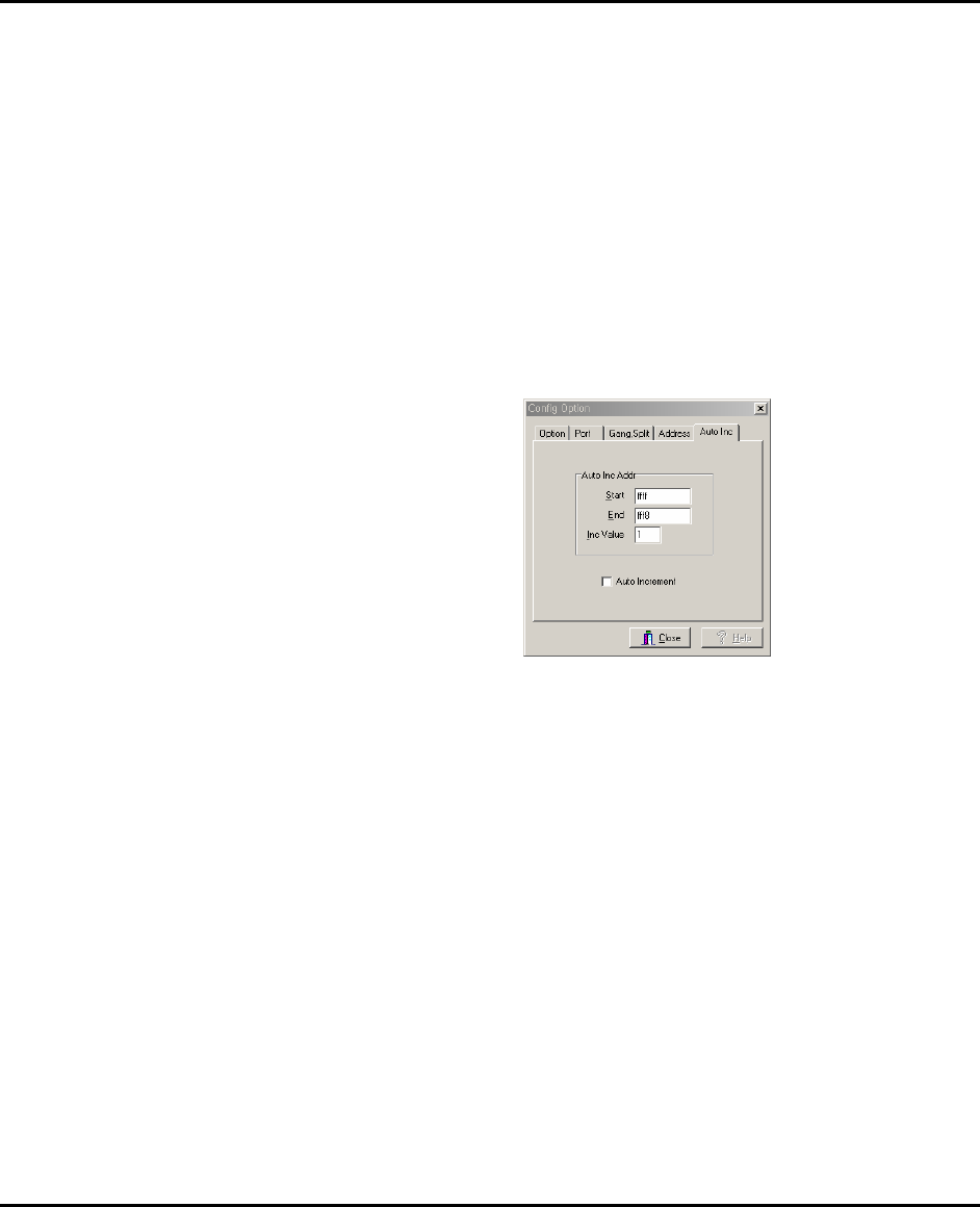
NOTE: The feature allows users to program a certain area that
might contain a serial number in the memory device with
serialized number by a certain value.
Start : Start address of memory that contains serialized data
End : End address of memory
Inc Value : This value will be added to the previous data value
User must click on Auto Increment to program a memory
with data increased by one to the previous data.
File
ProView uses three different file types: BINARY, ALL HEX, and POF. In the file
type box, a file type can be selected and loaded to the buffer or saved onto a disk. The
default file type is the Binary file. The All HEX files can be chosen by maneuvering
the arrow button. All HEX files include INTEL HEX (MCS-80/86/386, MOTOROLA
S (1-9), Tektronix HEX and ASCII HEX. OPF (Programmer Object File) is a binary
file generated by Altera assembler (Quartus and MAX+PLUS II). This file should be
loaded for Altera MAX or EPC family devices only.

Proview User’s Guide
27
Binary Format
Binary format does not specify the address or checksum of the file. The file
contains the actual binary data. An example of this format is a DOS executable
file with an .EXE or .COM extension. Binary format is generated for
programmable memory devices. It is recommended to save your EPROM data
as binary format in order to load the file as a standard file format later.
Intel HEX Format
Intel HEX format files are text files that include the file information in
hexadecimal.
1 : A record mark
2 – 3 Byte Record length in 2 digit HEX, Max 20 (64 in
ASCII)
4 – 7 Address 4 digit HEX Field. Most significant byte first
8 – 9 Byte 2 digit field record type :
01 End of file
02 Extended address
10 – N Data Data field in HEX digits
N+1 – N+2 Check-Sum Two digit HEX Check-Sum character computed
by two’s complementing the sum of previous
bytes except the ‘:’
INTEL HEX FILE EXAMPLE
:110000000444154414D414E2053332053455249414C73
:00000001FF
The extended address record specifies the index address where data will be
loaded into. The Extended Address will continue to offset data record address
until a new Extended Address record is specified.
:02 0000 02 4A29 02
Check Sum
Index address
Record type
Address
Record Length
• The Address field is blank because this record is not data.
• The record length is '02' for index address (2 Bytes).

Proview User’s Guide
28
NOTE: If the address for the data record is '2B56', the actual address
will be 4A290 + 2B56 or 4CDE6(HEX).
Motorola S HEX Format
The Motorola S format file is an ASCII-HEX file.
Position (Byte) Character Remarks
1 S Letter S indicates start of record
2 0, 1, 2, 3, or 9 A single character indicates the type of
record.
9: End-of-file
3: 32-bit address data record
2: 24-bit address data record
1: 16-bit address data record
0: Header
3 - 4 Byte Byte COUNT in HEX (multiply by two
for number of characters). This count
includes the address, data, and
Checksum field.
5 - X Bytes Memory Address for the current record.
X will be:
8 : 16-bit addressing for files less than 64K.
10: 24-bit addressing for files greater than 64K.
12: 32-bit addressing for files greater than 64K in length.
X+1 - N Bytes HEX Data (two per byte)
N+1 – N+2 Check-Sum Two digit HEX Check-Sum character
calculated by one’s complement
of DATA, ADDRESS and COUNT.
Motorola File Example
S1140000444154414D414E2053332053455249414C6F
S9030000FC
TEKTRONIX HEX Format
The Tektronix HEX format contains ASCII records, expressing bytes ASCII
pairs.
Position Character Remarks
1 / Slash character for start of line
2 - 5 2Bytes Address. MSB first load
6 - 7 Byte Number of data bytes (not checksums)
8 - 9 Byte Check-Sum of ADDRESS and COUNT
by character in HEX (not by byte)
10 - N Data Data bytes as ASCII pairs

Proview User’s Guide
29
N+1 - N+2 Byte Check-Sum of Data by character (not as
bytes)
Tek Hex Example
/00001102444154414D414E2053332053455249414C8F
/01000001
ASCII HEX format
This selection generates an ASCII coded HEX format for either 4-bit or 8-bit
PROMs. Each record contains a four-digit HEX address (16-bit) followed by 16
data elements. A 16-bit checksum is at the end of the file.
When this format is selected, the device base address must be specified. This
address represents the lowest address in the device. The file created contains an
entry for each location in this device. ASCII HEX format can be created for
programmable memory devices only.
JEDEC Standard <PLD devices only>
JEDEC (Joint Electronic Device Engineering Council) files are the standard
method for describing PLD fuse patterns and test vectors. JEDEC files contain
fuse data, test vectors, part numbers, and checksums. The checksum of the file
allows you to verify that a given file is intact and has not been unintentionally
modified. JEDEC files normally use the extension (last 3 letters) “.JED.”
For more information on the JEDEC standard, contact:
Global Engineering Documents Inc. at (800) 854-7179
Electronic Industries Association at (202) 457-4900.
Following is an example of a JEDEC file:
<STX>File for PLD 15S8 Created on 11-SEP-96 5:08PM
2754 memory decode 345-432-123
Seung Park PK Logic corp.
QP20* QF448* QV8*
F0*X0*
L0000111110111111111111111111111*
L0028101111111111111111111111111*
L0056111011111111111111111111111*
L0112010110110111101111111111111*
L0224011110111011101111111111111*
L0336010101110111011111111111111*
V0001000000XXXNXXXHHHLXXN*
V0002010000XXXNXXXHHHLXXN*
V0003100000XXXNXXXHHHLXXN*
V0004110000XXXNXXXHHHLXXN*

Proview User’s Guide
30
V0005111000XXXNXXXHLHHXXN*
V0006111010XXXNXXXHLHHXXN*
V0007111100XXXNXXXHHLHXXN*
V0008111110XXXNXXXLHHLXXN*
C124E*<ETX>8646
STX The fuse map begins with an ASCII STX character
(02 HEX)
Design Specification This item is user specified. While no format rules
apply, certain information, such as user’s name,
company, design date, part designation, revision and
device part number, should be entered. This field is
illustrated by an asterisk (*).
QP Specifies the number of pins in the devices.
QF Specifies the number of JEDEC fuses in the devices.
L The fuse list fields contain the state of all fuse links in
the devices. The starting fuse number follows the L
specifying the field type. The fuse list that follows
contains a zero (0) for each intact link and a one (1)
for each blown link. An L field is generated for each
product term in the device.
C The checksum field contains the 16-bit sum of the
link stated in the 8-bit words.
ETX The fuse map ends with an ASCII ETX character (03
HEX).
Sum Check A 16-bit sum of the ASCII values of the characters
from STX to ETX inclusive. The sum check follows
the ETX.
NOTE: LOGIC Compilers For PLD Devices: Software is available to
help the engineer develop designs using PLDs. Software tools called
logic assemblers or compilers translate a design file written in high-level
language into a fuse pattern stored in a JEDEC file. JEDEC files are
produced by almost all PLD development software’s and are accepted by
the ProView (TopMax/SpeedPRO 800(400)/SpeedPRO
S800(S400)/ChipMax/TopMax2/UniMax/ProMax8G(4G)) programmer.
There are many commercial software packages available to help you
design using PLDs.
POF file <Altera EPMxxx devices only>
The programming object file (.pof) for an EPM7128A or EPM7256A device can
be programmed into the EPM7128AE or EPM7256AE device, respectively,
using the MAX+PLUS® II software version 9.6 and later or with 3rd party
programming software from EE Tools programmers.
For further question on POF file, contact http://www.altera.com/support/spt-
index.html.
Proview User’s Guide
31
File / Load
Data can be loaded into the memory from a device or by opening a data file.
Load fills your buffer memory with the data from storage for viewing or editing.
This command loads the data from the selected file storage into the memory
buffer. In order to the use “All HEX File” selection, the HEX file must be one of
the file formats supported by the ProView(SpeedPRO/SpeedPRO
800(400)/SpeedPRO S800(S400)), such as Intel HEX(MCS-80/86/386,
MOTOROLA S(1-9), Tektronix HEX and ASCII HEX.
The default selection on File Load menu is in Binary Format. To select any of
the HEX files mentioned above, choose “All HEX File” by pressing ⇓ button.
When you have selected the desired file, press the OPEN button to load the file
into the data buffer. If you are programming a PLD, you will want to load a
JEDEC file. The procedure is identical to loading a data file, except that the
files in the current directory will have the JED extension. If your selected
device is an Altera MAX family, the file you should load is a POF extension.
The ProView uses a RAM buffer to hold data. After loading a file into the
buffer, you can edit the buffer data. If you load a JEDEC file, you may use (the
vector pattern edit) command to view or edit the fuse map and (test/vectors) for
any test vectors that may have been in the JEDEC file.
File / Reload
Data can be reloaded into the memory from the file directories that contains
previously loaded files. Reload remembers your file location and type (Binary or
All Hex) that has been loaded into the buffer.

Proview User’s Guide
32
File / Save
Save the current data in your memory buffer to a disk storage by using one of
the current supported file formats.
Before saving a file, check the buffer and the file address ranges. The contents
of the buffer through the specified range will be written into the new file,
completely erasing any existing file with the same name. Before saving to a
disk, make sure that no file with the same name exists.
File/ Load Project
A project file that saved by SAVE PROJECT menu is loaded. The project files
use the extension (last 3 letters) “.prj.”
File/ Save Project
This feature allows you to create a job description such as “engineer name” and
other useful information for records.
It is very useful for future use when you set up all possible environments such as
selecting a device, loading a file, and setting other configurations for
programming jobs. A job description can be saved as a file name and the same
project environment will be ready once you load the same project name.
File Name: A file name can be entered with the 3 letter extension “.prj.”
Author: An engineer’s name [whom creates this project].
Description: A job explanation that you memorize for your future usage. A
device number, File name, and checksum number can be entered in the note pad.
Other programming menu descriptions, such as configurations can be described.
Buffer
Buffer / Edit Buffer
This command allows the user to examine and modify the contents of the
memory buffer. This section applies to a non-JEDEC file (PROM, EPROM,
EEPROM, and Microcontroller) or to a memory chip. If a PLD is being loaded,
see the (vector pattern edit) section. The data is presented in HEX and ASCII
formats.
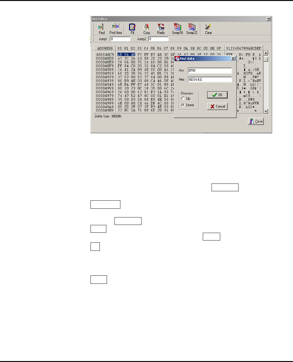
Find
This feature allows you to search the data (ASCII and HEX) in the current
Proview User’s Guide
33
Asc : The data looking for ASCII value.
HEX : The data looking for HEX value.
Direction UP : The data searching from previous address than the current
location.
Direction DOWN: The data searching from higher address than the current
location.
If you would like to find more data, click on the Find Next button.
Find Next
Press the Find Next button to locate the rest of the data that you entered in the
FIND box. The error “Search Pattern not Found” will be accursed when you
press this button without entering data in the FIND text box.
Fill
Buffer Start: Starting address for the data to be filled in buffer.
Buffer End: Ending address for the data to be filled in buffer.
Fill Data: Two digits of HEX value to be filled between Start and End buffer.
Copy
Buffer Start: Starting address for data to be copied.
Buffer End: Ending address for data to be copied.
Destination: Start address for data to be pasted.
Proview User’s Guide
34
Radix
Pressing this button will display the address value in decimals (using 0-9) or
HEX (using 0-9,A-F). The information appears on ADDRESS column at the left
of the buffer screen.
Swap16
This option applies to the current buffer data. Pressing this button allows you to
swap 8-bit data from ODD address to EVEN address.
Swap32
Pressing this button allows you to swap 16-bit data from ODD address to EVEN
address.
Clear
Pressing this button allows you to fill the buffer with the data located in “Default
Buffer Value” in Config Option Menu.
Close
Press to exit the HEX Editor.
Buffer / Edit UES
The UES Edit command creates or changes the User's Electronic Signature
(UES) array in GAL device. Each GAL device contains an electronic signature
word consisting of 64 bits of reprogrammable memory. The electronic signature
word can be programmed to contain any identification information desired by
the user. Some uses include pattern identification labels, version numbers, dates,
inventory control information, etc. These features give the user the ability to
view and edit the UES data before programming a GAL device.
When the UES edit command is invoked, an editing data window appears. If the
data fields are empty, you may create a new UES. You can enter the UES up to
eight characters in the HEX or ASCII data area. If you see any data from the
current UES window, it means the UES has been created and that you can
modify the data for a different reason. The UES data is not secured when you
execute the Function / Security command.
Proview User’s Guide
35
Device
This section presents the main operation menu for the target device that is
mounted on the ZIF socket. In order to process the following commands, make
sure that the device is correctly inserted into the ZIF socket and the latch is
down.
NOTE: The Device Information display area presents the device
information of the selected device.
Proview User’s Guide
36
Select
During operation, the first step is usually to select a device. This Select
command enables the user to define the manufacturer and the type of the device
that will be used. After you select a device, you can insert a device into the
programmer’s device socket and conduct various device operations such as
programming and verifying device data or reading data from the device. The
Select command contains both manual and automatic methods for selecting a
device. If your device is not identified by the Auto Device Select menu, you can
select the device list displayed in the Manufacturer & Device list. Scroll through
the manufacturers and device numbers until you find the manufacturer and
device you are looking for. You can use wildcards to help you “zoom” on the
device you are looking for.
NOTE: PAL Device Logic Symbols: The logic symbols for each of the
individual PAL device gives a concise functional description of the PAL
device logic function. This symbol makes a convenient reference when
selecting the PAL device that best fits a specific application
Select / E(E)PROM, FLASH
All EPROMs (27xxx), EEPROMs (28Cxxx, 29Cxxx), Serial E(E)PROMs
(17xxx, 24xxx, 32xxx, 33xxx, 35xxx, 59xxx), and Flash EPROM (28Fxxx,
29Fxxx, 29LVxxx, 29BVxxx, 29Wxxx, 49Fxxx) of 24/28/32/40/42 and up to 48
pins (1 Mbit, 2Mbit, 4Mbit, 8Mbit,16Mbit, 32Mbit, and up).
Select / PLD
EPLD, EEPLD, FPL, PEEL, GAL, MAX, MACH, PLS, PLD, PLC, PLUS,
EPM, ATFxxx, ATVxxxx, EPxxx, EPCxxx, 5Cxxx, 85Cxxx.
Proview User’s Guide
37
Select / Microcontroller
Intel 87xx, Phillips 87C75x, SGS-Thomson ST62xx, Atmel AT89Cxx, 89Sxx,
89LVxx, Microchip PIC12/16/17, Motorola MC60705xx,
MC68HC711xx/705xx; Zilog Z86Exx; NEC 8749H.
Select / PROM
AMD 27Sxx, Cypress CY7Cxxx, Fujitsu MB71xx, Fairchild 63Sxx, NS 74Sxxx,
Phillips 82Sxxx, WSI 57Cxx.
Select / Auto Select
Identify the device that is mounted on the ZIF socket. This feature can only be
applied to Memory and some Microcontroller devices. Clicking the Auto
Select button will enable the programmer to identify the ID on the device and
will select the matching device in the library automatically.
NOTE: If you have a “Device not found" message, select the device
manually. If you have old devices or defective devices, TopMax will not
be able to recognize the ID code from your device.
Device / Change Algorithm

Proview User’s Guide
38
Users are provided with an option of changing the programming parameters of
most devices. Once you select the “Change Algorithm” option under the
DEVICE menu, the user will be presented with a list of device specific
programming parameters, such as Vccp, Vpp, Read Vcc, Verify Vcc Low,
Verify Vcc High, Pulse Width, Over Pulse Width, Over Pulse Mul, and Retry
number. Each of these parameters can be selected and edited individually by
changing the existing numbers in the parameter box and pressing the close
button. The user will then be prompted to enter the new value for that parameter.
CAUTION: Please note that before deciding to modify any
programming parameter, the user must consult the manufacturer
programming specification for that device. Compass Systems will not
be responsible for any damages caused by any unauthorized modified
programming parameters. Any changes in programming parameters
are temporary and the original parameter’s value will be restored once
the operation on that device is complete. However, the user can store
the modified programming parameter for a particular device by using
Macro command.
Device / Blank Check
The Blank Check function is used to verify whether or not a device is in an
erased or unprogrammed state.
All EPROM (Erasable Programmable Read Only Memory) devices should be
checked before programming. EEPROM (Electrical Erasable Programmable
Read Only Memory) based parts do not need this command because EEPROM’s
are erased automatically before programming.
PLD based parts are checked by verifying all of the fuses that are intact. Any
erased PLD’s should pass this test.
NOTE: Erasing EPROMs. In order to clear data in an EPROM, the
chip should be exposed to a short wave UV (Ultra violet) light. Most
erasers require between 5 and 30 minutes to erase an EPROM. Some
types of chips take longer to erase than others. An EPROM based part
(a PLD or Microcontroller) with a security bit feature is designed so
that the security address is typically the last bit to be erased. If the
window of a chip is not clear, try cleaning the window with alcohol or
a solvent. Erase chips if the chips are exposed to sunlight and
fluorescent light for months or years; your chips can be erased. You
should cover the window of the programmed chips with an opaque
label to make the data permanent. Some EPROM based parts can't be
erased because they do not have a window. These chips are called one
time programmable (OTP) EPROMs.

Proview User’s Guide
39
An EPROM has a quartz window located on the chip just above the die. An
EPROM is erased by exposing it to high-frequency ultra-violet light waves.
Erasing an EPROM usually takes from 15-20 minutes, but may be shorter or
longer, depending on the device. Many manufacturers make EPROM erasers. If
you wish to purchase an eraser, call Compass Systems at +82-2-2109-8660.
When an EPROM is not being erased, the window may be covered with an
opaque label. Sometimes (over a period of years) an EPROM will start to erase
due to the level fluorescent light in the room. Direct exposure to sunlight also
has this effect and happens much more rapidly and commonly.
NOTE: In order to decide if the device is blank, the user should read
the target device. If the buffer is filled with all FFs or 00s, the device is
most likely in an erased or unprogrammed state; otherwise, the device
is not erased.
CAUTION: Some devices such as Philips P98C52 can pass the
BLANK CHECK routine after they are secured even though they are
not blank.
Device / Program
Program command will enable you to place new data from the memory buffer
into the target device. The BUSY GREEN led will be blinking during
programming. Make sure the device is correctly inserted into the ZIF socket and
the latch is down. Then check the buffer device address range before you start.
The values will default to the size of the device.
NOTE: <MOTOROLA MICROCONTROLLERS>
The window of windowed devices must be covered with an opaque
label during operation at all times.
NOTE: For all DEVICE/FUNCTION operations, the ERROR
YELLOW LED, located at the bottom of the ZIF socket is used to
indicate the status of the complete operation. It will turn on if an error
has occurred; otherwise it will remain off.
Memory device
The target device must be blank checked unless the part is electrically erasable.
Although most of EEPROMs and Flash Memory devices have the ERASE
function in the menu, some EEPROMs such as AT28CXXX or AT29CXXX
don’t have the ERASE function. Note that EEPROMs without the ERASE
function are automatically erased before programming.
Programmable Logic Device operation
After programming is complete, verification should be performed according to
the semiconductor manufacturer's specifications. In order to test vectors, a

Proview User’s Guide
40
vector test should be performed (See vector test under the TEST menu). Finally,
the part may be secured so that its content can no longer be examined or
modified. The security function will not execute if the device fails to verify or
pass the vector test properly.
28C256, 28C010, etc.
28CXXX family devices support Software Data Protection. The user has an
option of either protecting or not protecting the data. This option must be
changed before the start of any programming operation. To change this option,
go to the Option selection under DEVICE/FUNCTION menu and make any
changes accordingly. To obtain more information about Software Data
Protection, please consult the device manufacturer’s specification.
Microchip PIC devices
Microchip PIC series is different from other Microcontrollers in that they have
an EPROM area as well as a CONFIGURATION FUSE. The configuration
fuse in the PIC family is used to setup Oscillator Type, Memory Code
Protection, Watchdog Timer, or Processor Mode, and etc. After
programming the EPROM portion, change the fuses of the items listed under
Option. Then you must program the configuration option in the Option menu.
Perform the following procedure:
1. Program the main memory
2. Click on the OPTION button
3. Set all of the configuration fuse in OPTION menu
4. Click on the Program configuration fuses button
You may also read the status of the Configuration Fuse under the OPTION
selection. In order to obtain more information about programming the
configuration fuse, contact Microchip technology at +1-602-786-7200 or consult
the appropriate data book.
Copy from a master chip to a new chip
1. Select the master device from select menu in Microcontroller.
2. Put the chip on the ZIF socket.
3. Click on the Device button and read the chip.
4. Click on the Option button and read the fuses.
5. Write down all of the option fuses [the memory protect must be disabled]
in order to copy the information from your master chip.
6. Place a new chip. It must be the same chip as the master chip.
7. The buffer still holds your master data and the memory portion.
8. Click on Option again and set all the fuses that you wrote.
9. (To change the option, use the arrow button in the selection box.)
10. In the same Option menu, Click on the program configuration fuses,
read and compare the fuses with your original device.
Proview User’s Guide
41
CAUTION: The PIC16C711, will be used as an OTP (one time
programmable) chip when you erase the secured device. You cannot
reuse the chip after erasing it, even though the PIC16C711 is an
erasable device.
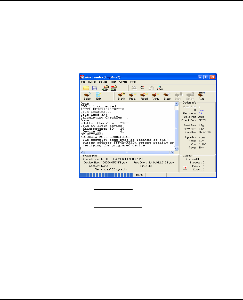
MOTOROLA MC68HC908 devices
This device will require a security code in certain memory location when you
program a new device along with data and users must remember the security
data once read(copy)or verify the master device for duplication.
Serial EEPROMs
These devices are electrically erasable, but they operate serially rather than
parallelly.
Atmel or Xilinx 17xxx
You need to set the POLARITY FUSE with this family via the Option menu.
After programming the main MEMORY, go to the OPTION menu and make the
appropriate change. On OTP (One Time Programmable) devices, the
POLARITY FUSE status cannot be reversed once it has been changed. Even on
some of the windowed 7xxx family devices (excluding Xilinx 17xxD/L &
17128), the POLARITY FUSE cannot be toggled. Consult the device
manufacturer for further instructions on how to handle the Polarity FUSE.
CAUTION: Do not touch or remove a device during an operation
when the BUSY green led is on.
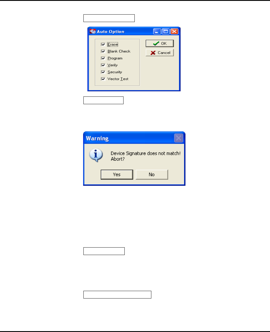
Proview User’s Guide
42
Auto Menu Option
Device / Read
Read the data in the source device mounted on the ZIF socket into the buffer for
examination.
The checksum will be displayed on the checksum line. The buffer may be edited,
saved to a disk, or used to duplicate the chip.
CAUTION: Reading the device into the buffer destroys the buffer
contents through the specified range. Make sure everything in the
buffer that is needed has been saved.
PLD test vectors are not stored in a logic device; therefore, they cannot be read.
The test vector buffer will be empty after reading the PLD.
NOTE: Devices that have been secured cannot be read properly.
Secured chips may appear all blank, fully programmed, or scrambled.
Device / Verify
Assure that data in the device matches data in the memory buffer. If your device
has the security fuse blown, a verification error is detected. The verify operation
requires that the exact data pattern or file that was used to program the device be
resident in the memory buffer.
Device / Data Compare
Compares the data in device to the data in buffer and saves any difference into
the COMPARE.TXT file. When you have a verify error during the Verify
operation, the Data Compare command will be useful. It will detect a
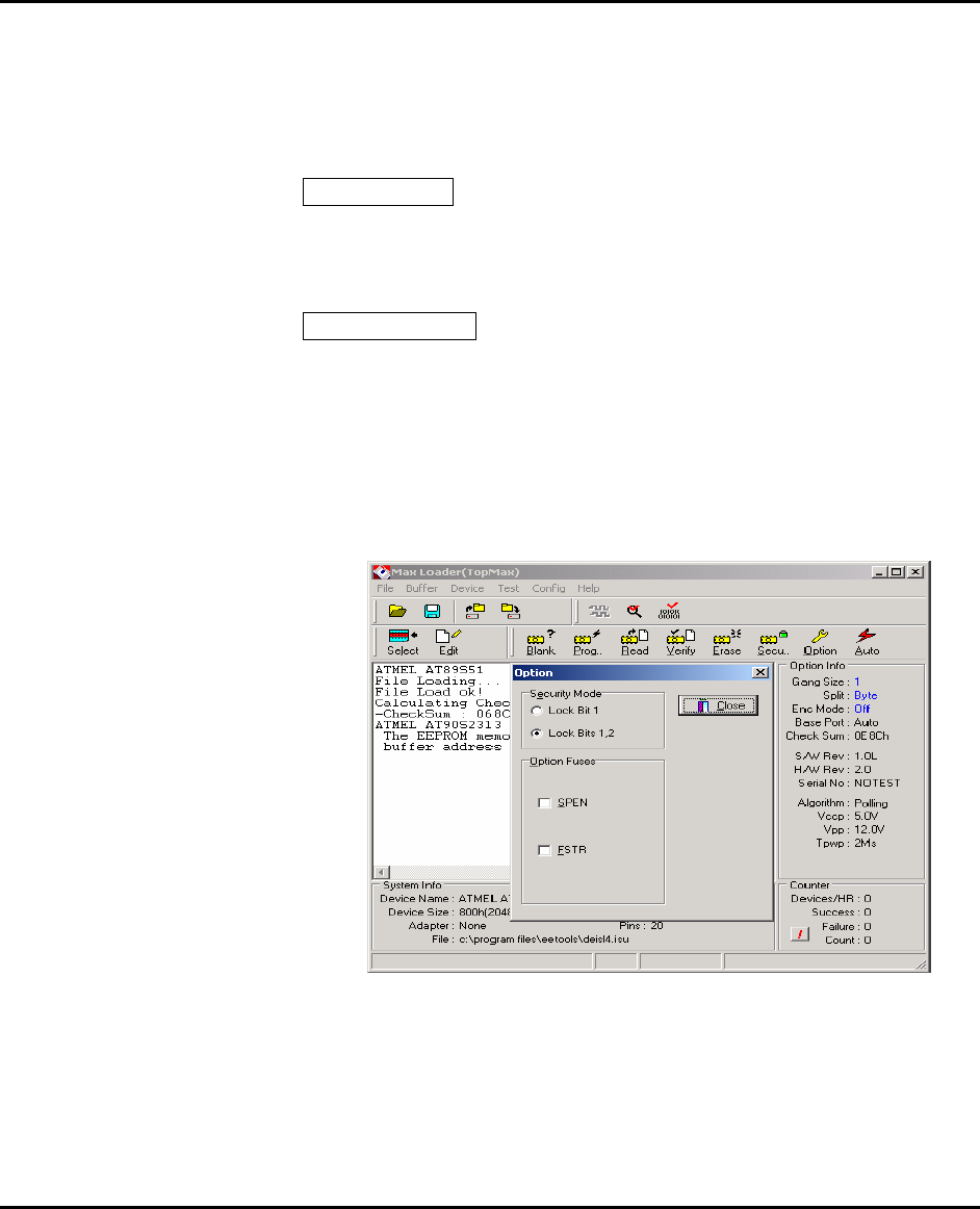
Proview User’s Guide
43
difference between the device content and the buffer content and will write the
difference into the COMPARE.TXT file under the ProView
(SpeedPRO/SpeedPRO 800(400)/SpeedPRO S800(S400)) directory. You may
view the file using edited utility software.
Device / Erase
This option erases the data in your socket before programming it. This operation
is valid for only limited devices such as EEPROM, Flash Memory, GAL, PEEL
devices. EPROMs that have a window should be erased by UV EPROM erasers
externally (see NOTE “Erasing EPROMs” in this manual).
Device / Security
Secure a PLD or Microcontroller so that their content can no longer be
examined or modified. Security is confirmed when valid data can no longer be
read or verified against a previously read pattern. To ensure that the security
fuse has been blown, the Security operation is preceded by a “read” of the
device and followed by a “verify”.
NOTE: Usually, on a UV erasable PLD or a Microcontroller, a
secured device may take longer to erase because the security bit
address is designed to erase last.
NOTE: When you click on OPTION, device security mode and option
fuses will be available for certain manufacture devices. Selecting these
options, programmer will program your device with the checked
options continuously. It is a useful feature for users who like to
program devices in volume quantities. The user does not have to set the
fuses or security modes for every programming.
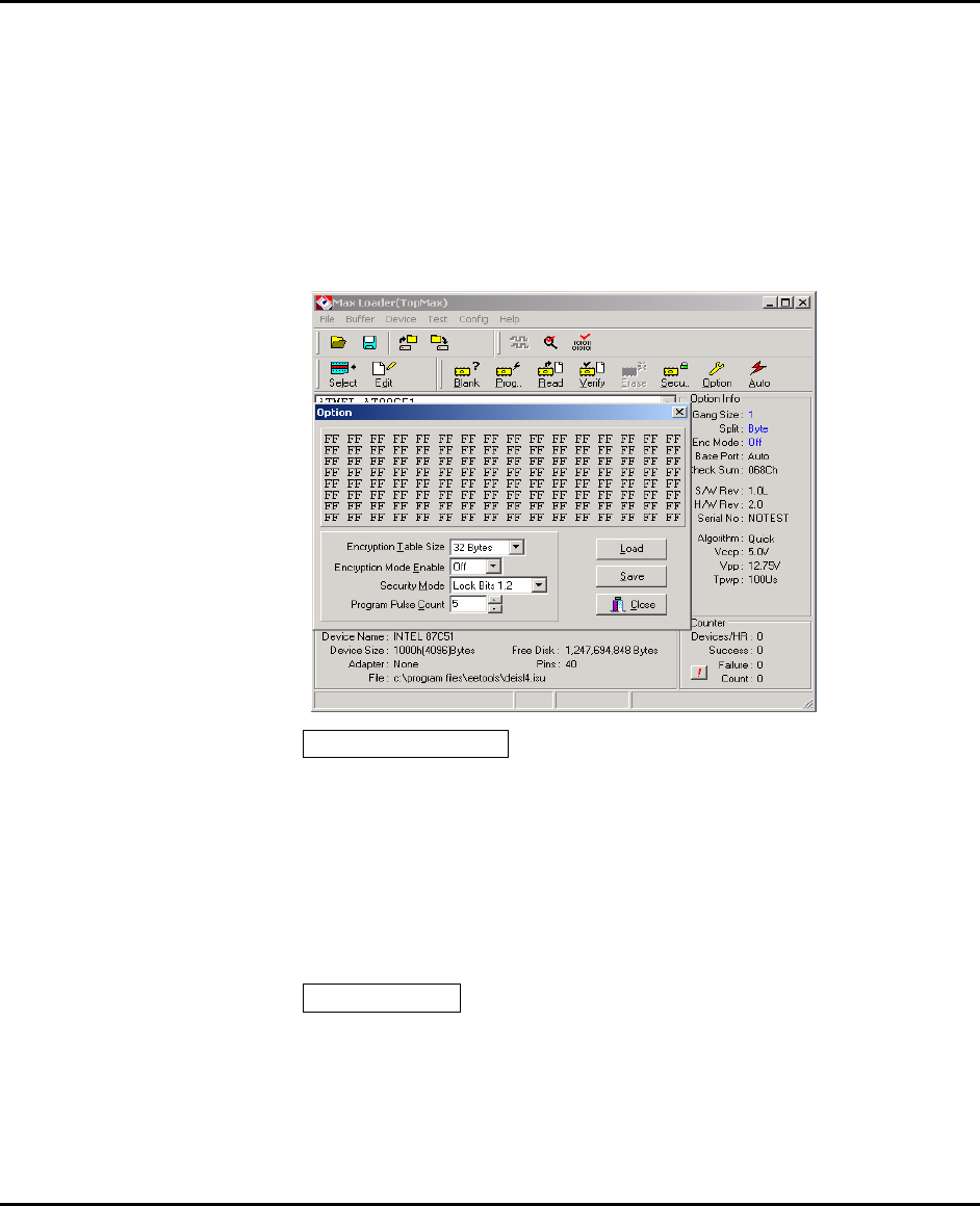
Proview User’s Guide
44
CAUTION: Some devices, such as Philips P89C52, can pass the
BLANK CHECK routine after they are secured. Securing a device
separates the programmed data pattern from unauthorized access.
This command appears only when the selected device supports it.
Some Microcontroller’s and PLDs can be secured by programming a
special address location. The security bit will be cleared when the
device is erased. Once a device is secured, it cannot be unsecured to
read, verify, or duplicate. Also the secured device is seen as a blank
chip even though it is not actually blank.
Device / Encryption
The encryption table is a feature of the 87C51/87C52 family Microcontroller
devices. The Encryption array of the Microcontroller is initially unprogrammed
(all '1's). In order to protect the code from being easily read by anyone other
than the programmer, this feature allows you to program the encryption table
that is exclusive NOR with the program code data as it is read out. You have to
know its content in order to correctly decode the program code data. Thereafter
you will have to use the same displayed encryption array any time you need to
read back the device.
Device / Option
○
1 Device/Option /Customer ID
The user can store checksum or other code-identification numbers.
○
2 Device/Option / Oscillator
Most PIC device family’s can be operated in four different oscillator modes. The
user can choose one of the following modes from the factory.
LP: Low Power Crystal
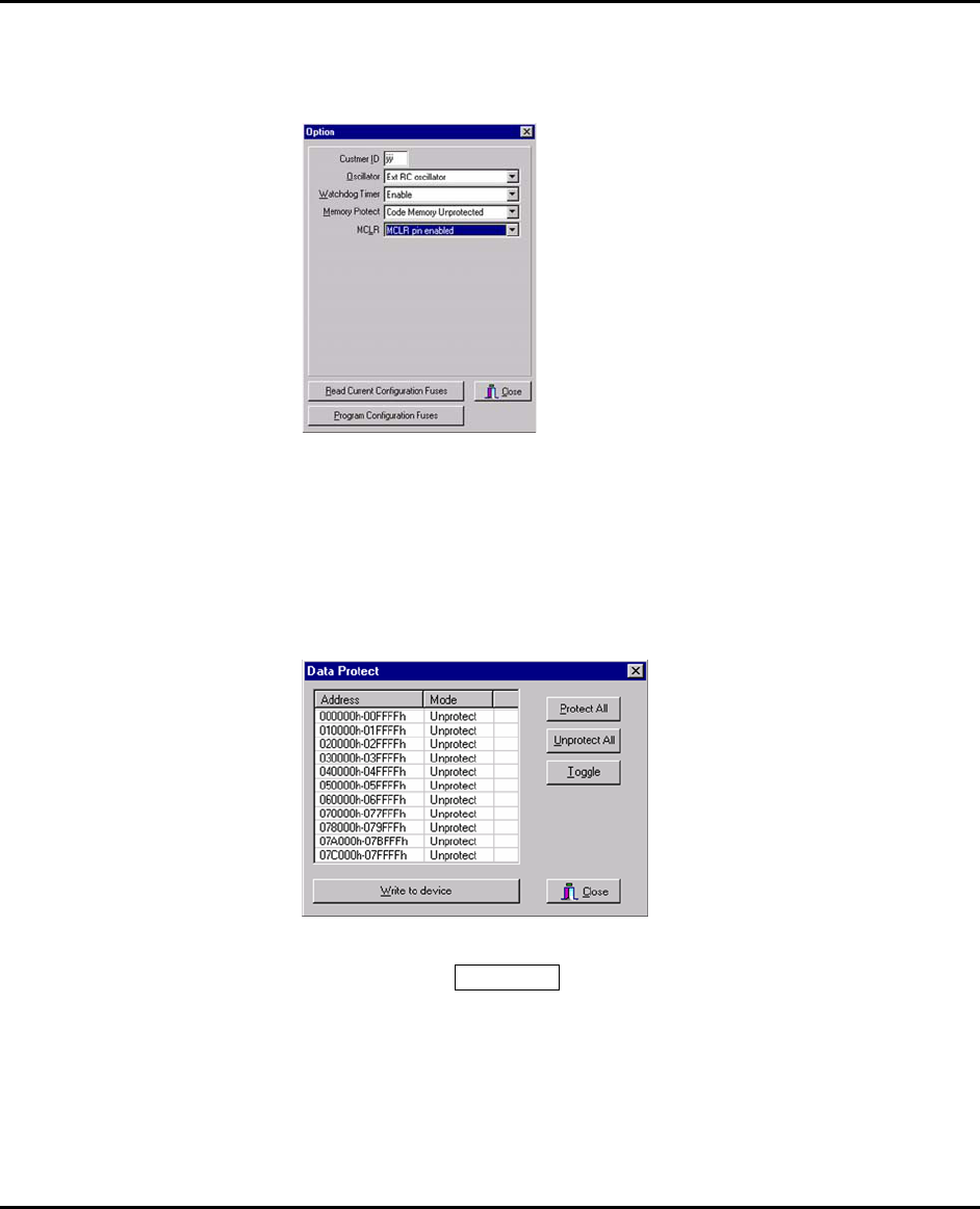
Proview User’s Guide
45
XT: Crystal/Resonator
HS: High Speed Crystal/Resonator
RC: Resistor/Capacitor
○
3 Device/Option / WATCHDOG TIMER (WDT)
WDT is a configuration bit of special features for PIC device family’s.
○
4 Device/Option / POWER-UP TIMER
This is a special feature for the PIC device family.
○
5 Device/Option / Memory Protect
This configuration fuse can be used to protect against spurious EEPROM writes.
○
6 Device/Option / Data Protect
This feature may be enabled or disabled by the user; when shipped from an IC
manufacturer, the Data Protect feature is disabled.
Devices have “Software Data Protection (SDP)” : Provides software features to
protect nonvolatile data from in advertent writes.
Disable: The SDP command will not protect the entire memory array.
Enable: The SDP command will protect the entire memory array.
Certain Flash device has “Sector Protection”
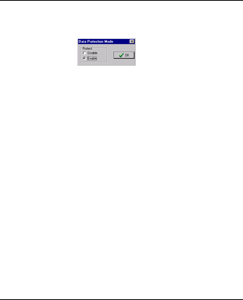
Proview User’s Guide
46
Protect All: By pressing the Protect All, no data will be erased or written into
the device. You can still read data from the device. The block(s) doesn’t allow
the device to be erased or programmed
Unprotect : The selected block(s) allows the device to be erased or programmed.
Toggle: Change the block status in reverse.
Write Device: The selected block status will be written in the device.
Close: Exit to main menu.
○
7 Device/Option / Reset Polarity
Reset Polarity (for Xilinx FPGA): The Polarity Fuse is ACTIVE HIGH when
shipped from an IC manufacturer. To change the polarity, click on the Option
button and check on the Reset bit box before programming your device. Once it
changes to ACTIVE LOW, it may not reset the ACTIVE LOW fuse to ACTIVE
HIGH. On OTP (One Time Programmable) devices, the POLARITY FUSE
status cannot be reversed once it has been changed. Even on some of the
windowed 7xxx family devices (excluding Xilinx 17xxD/L & 17128), the
POLARITY FUSE cannot be toggled. Consult the device manufacturer for
further instructions on how to handle the Polarity FUSE.
○
8 Device/Option / Drown Out
This is a special feature for the PIC device family.
○
9 Device/Option / MCLR
This is a special feature for the PIC device family.
○
10 Device/Option / Memory Parity
This is a special feature for the PIC device family.
○
11 Device/Option / Low Voltage PGM
This is a special feature for the PIC device family.
○
12 Device/Option / FLASH Write Enable
This is a special feature for the PIC device family.
○
13 Device/Option / Background DBG
This is a special feature for the PIC device family.
○
14 Device/Option / Brownout Voltage
This is a special feature for the PIC device family.
NOTE: All the Options above are described in the device
manufacturer’s data book. Make sure that you understand all
configuration features before setting the configuration fuses.
○
15 Option Item/Read Current Configuration Fuses
In order to have the information of all configuration fuses, press this button
and you can see all configuration data of the current device. Be sure that you
remember all the fuse’s information if you want to copy the configuration
information
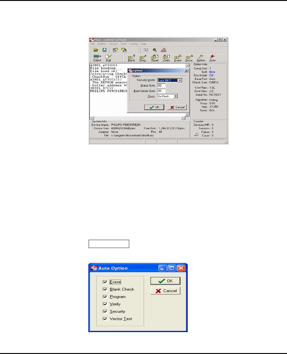
Proview User’s Guide
47
○
16 Option Item/Program Current Configuration Fuses
Pressing this button will store all configuration fuse’s information in the current
device located in the programmer socket.
○
17 Device/Option/Read Status Byte or Boot Vector
In order to have the information of option bits, press this button and you can see
all option lock bit data of the current device. Be sure that you remember all the
fuse’s information if you want to copy the configuration information.
○
18 Device/Option/Program Status Byte or Boot Vector
Pressing this button will store all lock bit information in the current device
located in the programmer socket.
○
19 Device/Option/Initialize Device
Initialize function erases the whole memory array, security lock bits, and status
byte and boot vector into their initial erased state. Pressing this button before
erasing all 89Cxx family manufactured by Philips.
Device / Auto
Auto command will enable you to do the following steps sequentially and it is
useful to program a volume quantity device with the same data.

Proview User’s Guide
48
CAUTION: Some devices such as Philips P98C52 can pass the
BLANK CHECK routine after they are secured without being blank.
Securing a device prevents the programmed data pattern into the
device from unauthorized access. This command appears only when
the selected device supports it. Some Microcontrollers and PLDs can
be secured by programming a special address location. The security
bit will be cleared when the device is erased. Once a device is secured,
it cannot be unsecured to read, verify, or duplicate. Also the secured
device is seen as a blank chip even though it is not actually blank.
Test
Test / Vector Test
Verifies that the PLD (PAL, GAL EPLD, etc.) behaves currently without having
to prototype a circuit. In order to perform test vectors, test vectors should be in
the JEDEC file when the file is loaded. Most PLD development software will
generate valid test vectors automatically. Test vectors may be examined and
modified with Vector Pattern Edit/^F6 command in the buffer menu screen.
NOTE: Due to hardware’s limitation, Vector Test is only implemented
on 24-pin or less devices.
During the vector test, SpeedPRO applies high and low signals to the input pins
of a tested PLD and observes signals at the output pins. The output results are
compared to the expected results from the test vectors. Any difference will
show up as an error message.
The following are valid characters for test vectors:
0 Apply input logic low (Vil) to an input pin
1 Apply input logic high (Vih) to an input pin
C Clock an input pin (Vil, Vih, Vil)
F Float pin
N Power pin or untested output pin
V VCC pin
X Don't care: output values are not tested
G GND pin
K Clock an inverted input pin (Vih, Vil, Vih)
H Expected result on output pin is Vih
L Expected result on output pin is Vil
Z Test for high impedance
Optional Operation
X value Optional value of “don’t care”
Vcc Test Vcc value on Vcc pin
Delay Test period of each vector in milli-second
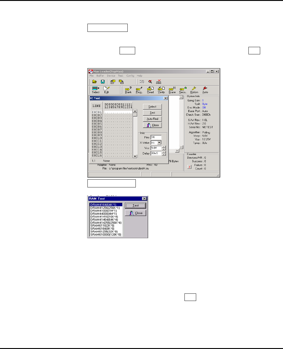
Proview User’s Guide
49
Test / IC Test
This operation tests TTL or CMOS logic devices according to the test patterns
stored in the test pattern library.
Click on the Select button and enter a device name and click on Test to begin
the test function. A result message will be displayed after testing.
Test / RAM Test
TopMax provides an additional memory test function. This operation tests static
and dynamic RAM memory chips. The following memories are tested:
DRAM types tested
- 16K*4, 64K*1, 64K*4, 256K*1, 256K*4, 1M*1
SRAM type tested
- 2K*8, 8K*8, 32K*8, 128K*8
After inserting a memory device into the ZIF socket, select the memory type
from your menu screen and click on the Test button.
The program will test each address of the memory. A "Defective memory"
message will be displayed with a current address if the memory has a defective
bit. "Good memory" will appear when the test has passed successfully.
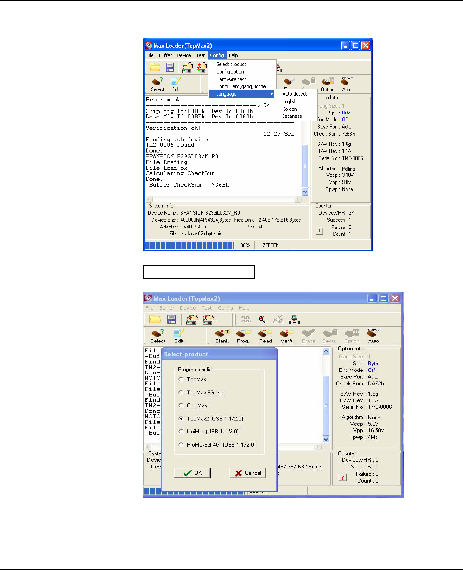
Proview User’s Guide
50
Config
Config / Select Product
After the ProView is installed, you can choose one of the programmer listed in
Select product menu.
Make sure that you select a right model and turn on the switch (SpeedPRO/
SpeedPRO 800(400)/SpeedPRO S800(S400)).
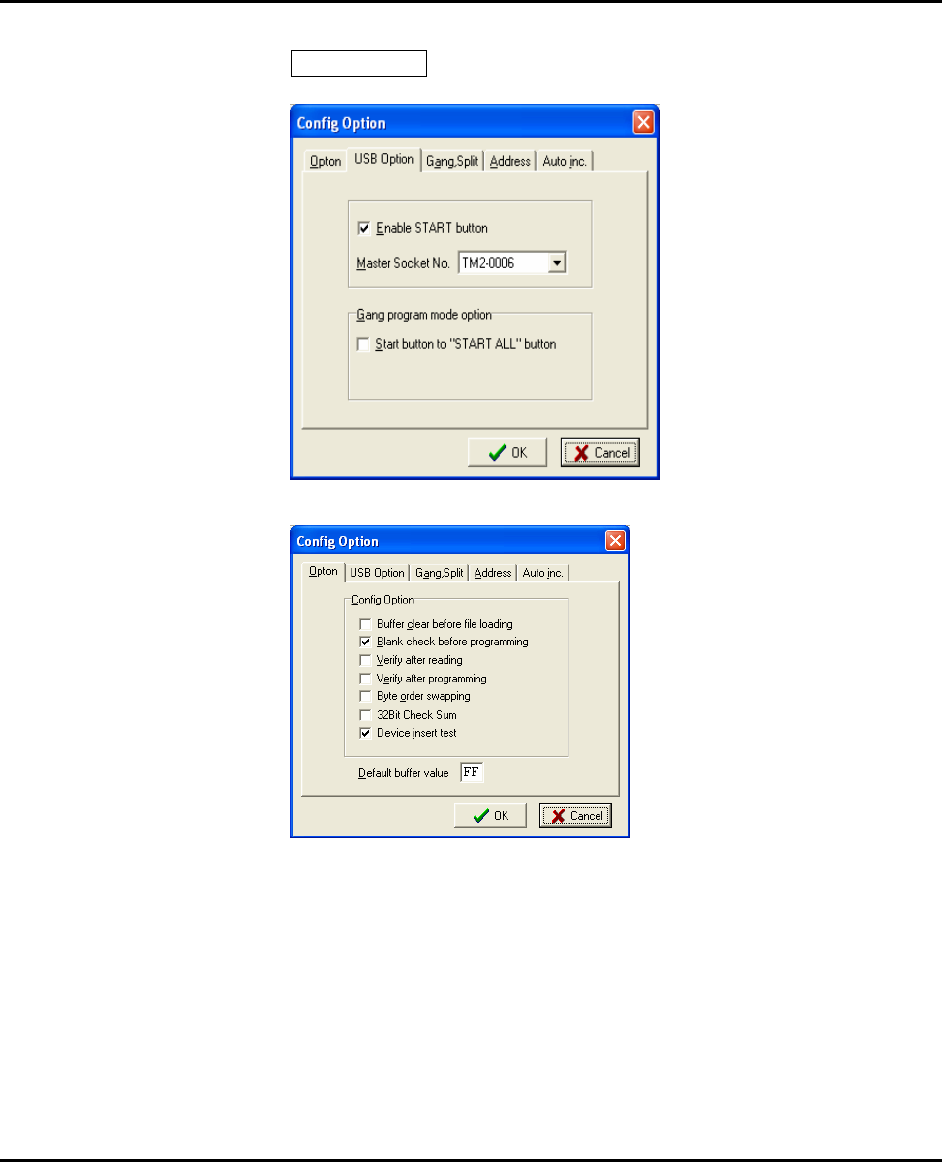
Proview User’s Guide
51
Config Option
Config Option / Buffer Clear Before File Loading
When loading a file into the buffer, executing the ENABLE option fills the
buffer with the data that is defined in Default Buffer Value before the file is
loaded into the buffer. When you load a file that is smaller than the current
buffer size, the unfilled buffer will contain the Default Buffer Value so that you
may examine the buffer data more conveniently. DISABLE option keeps the
same data for the unfilled buffer area after Buffer Load command is executed.

Proview User’s Guide
52
NOTE: Buffer Clear means that the current buffer will be filled with
the Default Buffer Value. It can be any data of Hexadecimal values
such as FF, 00, or XX
Config Option / Blank Check Before Programming
Enabling Blank Check Before Programming verifies whether the device is
erased before programming. Disabling Auto Blank Check Before Programming
prevents this check from occurring.
Config Option / Verify After Reading
Setting the configuration menu to ENABLE will allow you to verify whether the
device data is the same as the data in your current buffer after reading the source
device.
Config Option / verify after programming
Setting the option to ENABLE will allow you to verify whether the device data
is the same as the one in your current buffer after programming a device.
Config Option / Byte order swapping
This option applies only to 16-bit wide (E)EPROMs or Flash Memory. User
data is displayed in the buffer according to the Intel convention with the default
value set at Disable. Enabling this option allows you to use data according to
the Motorola convention during Program and Verify operations under the
Device selection. However, the data in the buffer is not physically swapped.
When enabled, the MSB (Most Significant Byte) of data is located to EVEN
addresses (0,2,4,...) and the LSB(Least Significant Byte) of data is located to
ODD addresses(1,3,5,...).
For example, Byte swap is useful if an assembler creates a file in Intel format, in
which the low byte is read before the high byte, but the file must be in Motorola
format, in which the high byte is read before the low byte.
Sample data file (Motorola EXORmacs Format, Code 87):
S00B00004441544120492F4FF3
S11300000123456789ABCDEF001122334455667750
S9030000FC
Data file opened with format 87 and displayed in the editor (8-bit addressing
mode):
CURSOR AT LOCATION: 00000000 8 BIT ADDRESSING
HEXADECIMAL ASCII
ADDRESS -0 -1 -2 -3 -4 -5 -6 -7 -8 -9 -A -B -C -D -E -F 0123456789ABCDEF
00000000 01 23 45 67 89 AB CD EF 00 11 22 33 44 55 66 77 .#Eg . . ”3Duf w
00000010 00 00 00 00 00 00 00 00 00 00 00 00 00 00 00 00
Example #1: Programming one 16-bit device (Data word width = 16, Odd/even
byte swap = disabled)
The user data is allocated as follows:
Device
MSB LSB
Device Address: 0 23 01
1 67 45
2 AB 89
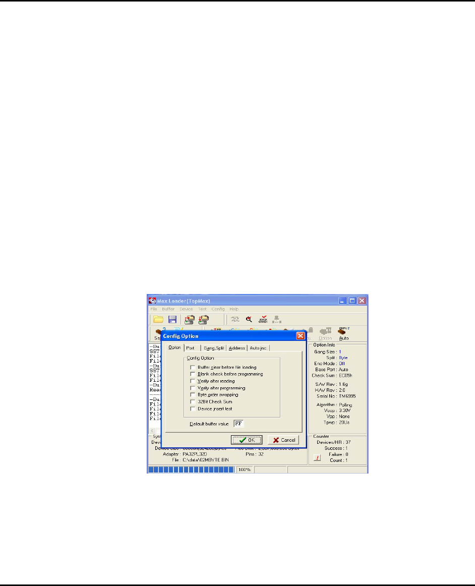
Proview User’s Guide
53
3 EF CD
Sample data file (Motorola EXORmacs Format, Code 87):
S00B00004441544120492F4FF3
S11300000123456789ABCDEF001122334455667750
S9030000FC
Data file opened with format 87 and displayed in the editor (8-bit addressing
mode):
CURSOR AT LOCATION: 00000000 8 BIT ADDRESSING
HEXADECIMAL ASCII
ADDRESS -0 -1 -2 -3 -4 -5 -6 -7 -8 -9 -A -B -C -D -E -F 0123456789ABCDEF
00000000 01 23 45 67 89 AB CD EF 00 11 22 33 44 55 66 77 .#E.g. . . ”3DUf w
00000010 00 00 00 00 00 00 00 00 00 00 00 00 00 00 00 00
Example #2: Programming one 16-bit device (Data word width = 16, Odd/even
byte swap = Enabled)
The user data is allocated as follows:
Device
MSB LSB
Device Address: 0 01 23
1 45 67
2 89 AB
3 CD EF
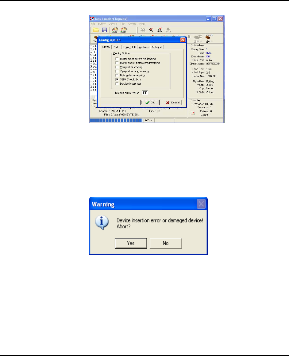
Proview User’s Guide
54
Config Option / Enable START Button
All Programmers have a START button at the socket location of the
hardware unit. The START button allows customer to program devices without
PC keyboard or software command. Once the button is enable, you can use the
START button as an automation key. Once you press the START button,
ProView will excute the “Auto” command stream sequentially to
Config Option / Device Insert Test
When enabled, this test will allow the ProView first examine the physical
position of a device as it is sitting in the programming socket when the user
attempts to take any action to that device. Once it has finished examining, the
ProView (SpeedPRO/SpeedPRO 800(400)/SpeedPRO S800(S400)) will prompt
the user for corrective steps if needed depending upon the position of the device.
Once you click on “Device Insert Test”, ProView (SpeedPRO/SpeedPRO
800(400)/SpeedPRO S800(S400)) will display “Incorrect device ID” if your
target device contains ID or if wrong device is placed inside the socket. You
may see the same message if the device has been secured or if the device ID has
been erased. Click on “Yes” if you want to ignore the manufacturer’s device ID
and proceed.
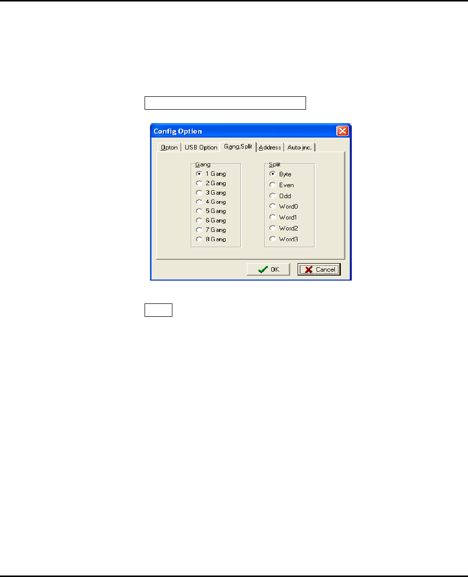
Proview User’s Guide
55
Config Option / Default Buffer Value
Fill the buffer value (hexadecimal) with the initial data that you type in this field.
This feature helps the user who wants to have different initial values ('00' or
'FF') in the buffer. Once you have made this change, exit to DOS, and restart the
ProView to get the result of the change.
Config Option / Gang Split Select
Gang
SpeedPRO 800(400)/SpeedPRO S800(S400) programs multiple E(E)PROMs
up to eight devices at the same time. In order to program multiple E(E)PROMs,
users must use SpeedPRO 800(400)/SpeedPRO S800(S400). SpeedPRO
800(400)/SpeedPRO S800(S400) is especially useful when it is necessary to
program many devices with the same data simultaneously. SpeedPRO
800(400)/SpeedPRO S800(S400) is designed for multiple programming and it
does not support set programming.
•SpeedPRO 800(400)/SpeedPRO S800(S400) can only be used for most
EPROM/Flash devices and cannot be used for GALs, PALS, etc. The software
will inform you when you try to select gang mode for an unsupported device.
• Place the SpeedPRO 800(400)/SpeedPRO S800(S400) on top of TopMax with
all handles pointing in the same direction as TopMax socket.
• If the device requires a PLCC adapter contact LDI, LLC, to obtain the correct
adapter.
• From the software menu Device/Gang Select, select 8-Gang Mode.
If you receive “Cannot be selected for 8-gang” message, then it is not possible
to program that particular device with the 8-gang adapter.
• Be sure that all devices are of the same brand, size and part number, otherwise
SpeedPRO 800(400)/SpeedPRO S800(S400) will not function correctly.
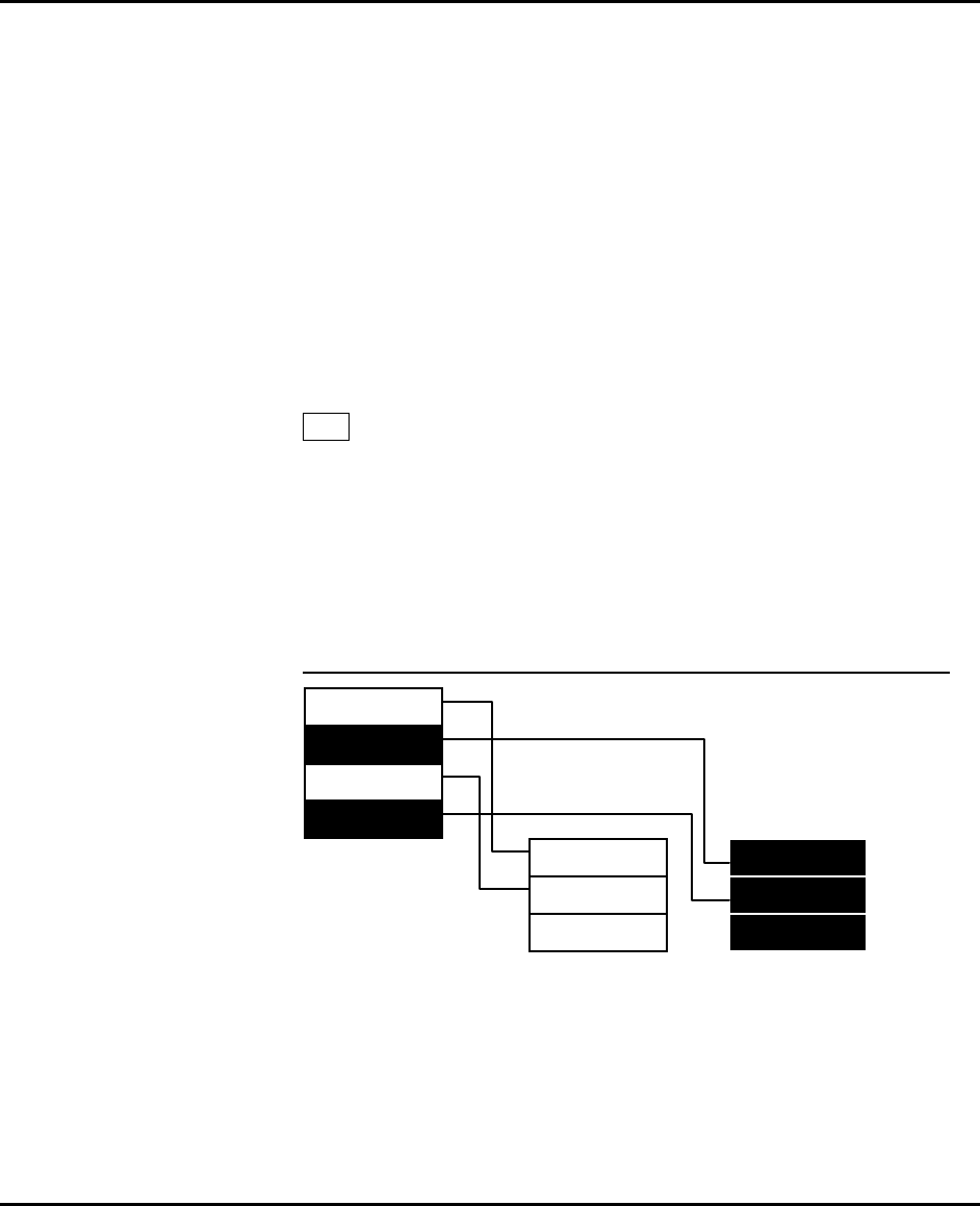
Proview User’s Guide
56
• If any (one) chip is defective, SpeedPRO 800(400)/SpeedPRO S800(S400)
will not Program/Verify/Blank Check any of the devices and you will get an
error message. Also note that a device may be defective even though the
BLANK CHECK passed.
CAUTION: The 48-pin socket should be used for universal devices
including PLD, and special Microcontrollers such as PICxx, 87C5X,
89C5X programming. Since SpeedPRO/SpeedPRO
800(400)/SpeedPRO S800(S400) adapter has 32-pin sockets, the
device support on SpeedPRO/SpeedPRO 800(400)/SpeedPRO
S800(S400) is valid for limited device programming such as
E(E)PROMs and Flash Memory. All of the devices should be inserted
into the socket with notch in the same direction as pictured on case.
Split
When programming devices for a 16-bit or 32-bit environment, you will need to
split your data onto two or four devices.
NOTE: SPLITTING DATA is different from SETTING DATA. Putting
buffer data into multiple devices is called “SET DATA”. ProView
(SpeedPRO/SpeedPRO 800(400)/SpeedPRO S800(S400)) doesn’t
support the SET DATA.
Split Programming Examples
EXAMPLE 1: PROGRAMMING TWO 8-BIT EPROM AS FOLLOWS:
Byte $0000
Byte $0001
Byte $0002
Byte $0003
Byte $0000 Byte $0001
Byte $0002 Byte $0003
::
1. Load a 16-bit file into the buffer.
2. Select the target device from menu.
3. Insert the target device (#1) into the ZIF socket.
4. Invoke EVEN in Split data menu.
5. Program the device (#1).
6. Remove the device (#1) and insert the second device (#2) into the ZIF socket.
7. Invoke ODD.
8. Program the second device.
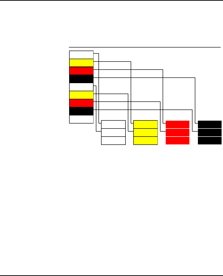
Proview User’s Guide
57
Now, you have two 8-bit EPROMs that have been programmed. The first
EPROM (#1) contains all the even address or low bytes and the second (#2)
device contain all the odd address or high bytes.
EXAMPLE 2: PROGRAMMING FOUR 8-BIT EPROMS AS FOLLOWS:
Byte $0000 Byte $0001 Byte $0002 Byte $0003
Byte $0004 Byte $0005 Byte $0006 Byte $0007
Byte $0000
Byte $0001
Byte $0002
Byte $0003
Byte $0004
Byte $0005
Byte $0006
Byte $0007
:
::: :
1. Select the target EPROM.
2. Load the HEX file (32-bit file) into the buffer.
3. Insert the first EPROM (#1) into the socket.
4. Invoke Word 0 in Split Data menu.
5. Program the mounted device.
6. Remove the programmed device (#1) and insert the second device (#2) into
the socket.
7. Follow the same steps as above.
After programming the 4th EPROM with Word 3, you will have four 8-bit
programmed EPROMs. The original file (32-bit) is split into four EPROMs
that contain 8-bit data in each device.
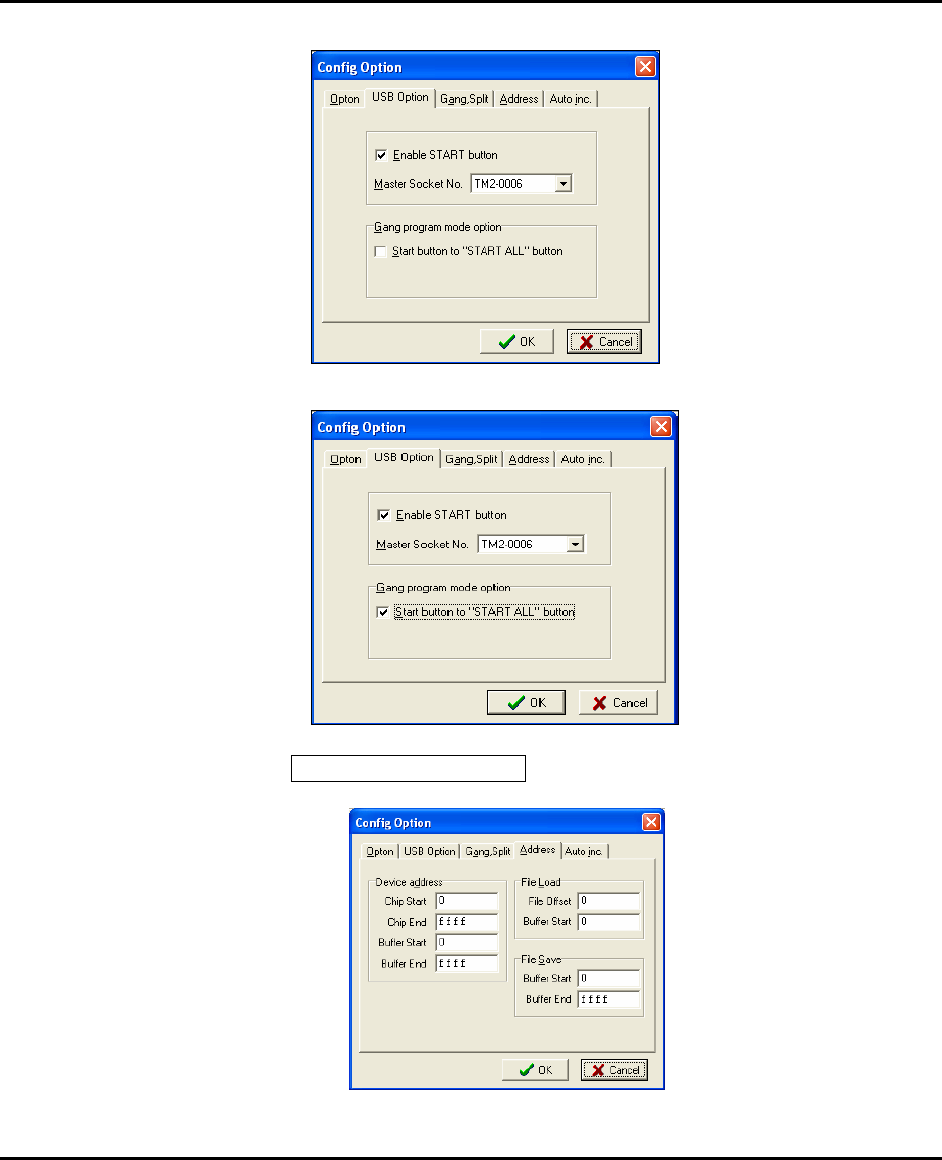
Proview User’s Guide
58
Config Option / Address

Proview User’s Guide
59
Device Address
These address will be applied for programming the buffer data.
-Chip Start: Device Starting address for the data to be programmed in buffer.
-Chip End: Device Ending address for the data to be programmed in buffer.
-Buffer Start: Buffer Starting address for the data to be programmed.
-Buffer End: Buffer Ending address for the data to be programmed.
NOTE: Device size for different devices
Device Device Address
2716 0 - 7FF
2732 0 - FFF
2764 0 - 1FFF
27128 0 - 3FFF
27256 0 - FFFF
27010/1024 0 - 1FFFF
27020/2048 0 - 3FFFF
27040/4096 0 – 7FFFF
File Load
These address will be applied for programming the buffer data.
-File Offset is subtracted from addresses from the file downloaded to the
programmer. For example, if you set File Offset to 1000h, then the downloaded
data minus 1000h would be placed into the buffer at the address specified by the
Buffer Start Address.
-Buffer Start Address is the address in the buffer where you want your
downloaded data to start. For example, if you set Buffer Start Address to 800h,
then the downloaded data only appears in the buffer beginning at address 800h.
File Save
These addresses will be applied for programming the buffer data.
-Buffer Start: Starting address for data to be saved.
-Buffer End: Ending address for data to be saved.
Proview User’s Guide
60
Config Option / Auto Inc
The feature allows users to program a certain area that might contain a serial
number in the memory device with serialized number by a certain value.
Start : Start address of memory that contains serialized data
End : End address of memory
Inc Value : This value will be added to the previous data value
User must click on Auto Increment to program a memory with data increased by
one to the previous data.
Config / Hardware test
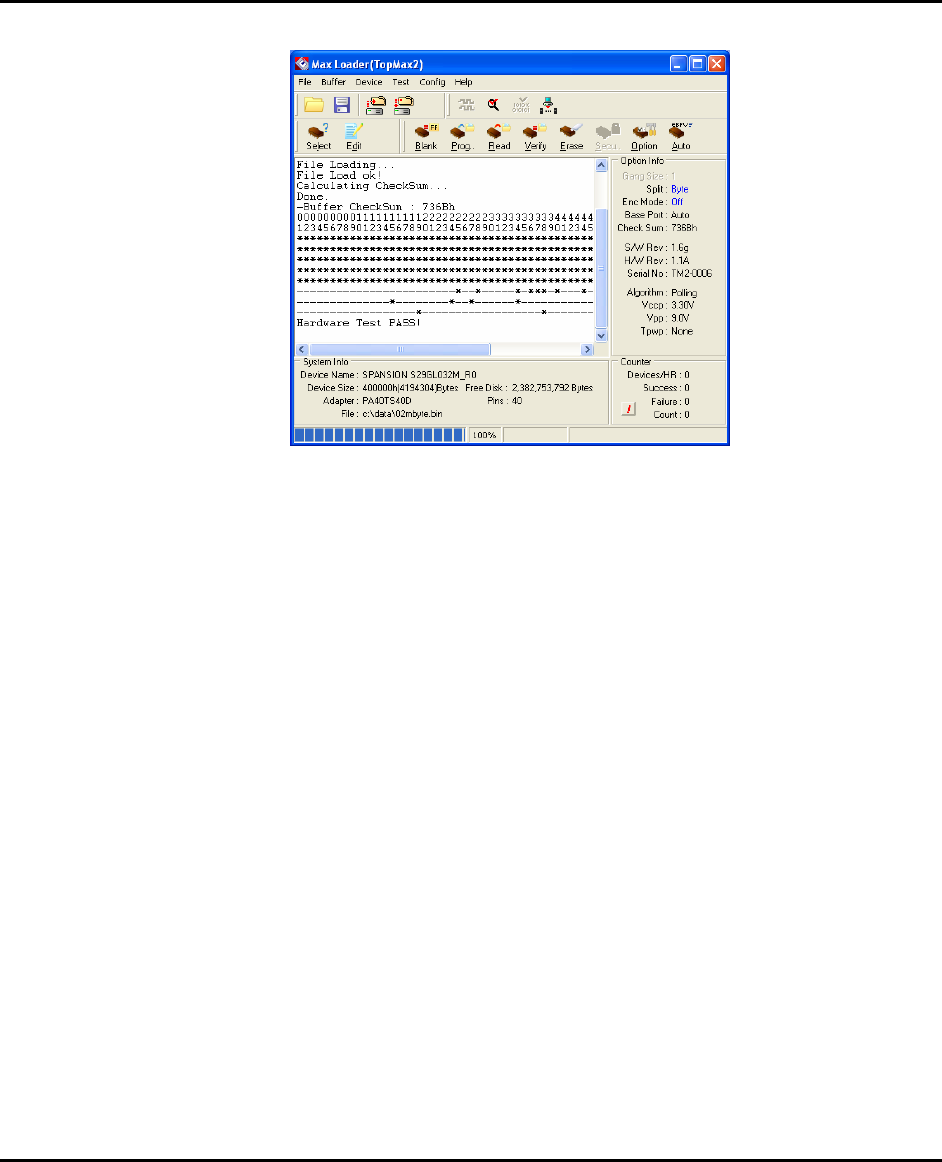
Proview User’s Guide
61
A hardware test is designed to assist customers in confirming and diagnosing
problems relating to (SpeedPRO/SpeedPRO 800(400)/SpeedPRO S800(S400))
programmer. If a hardware defect with (SpeedPRO/SpeedPRO 800(400)/
SpeedPRO S800(S400)) is suspected, we recommend the users to run this test in
order to confirm whether or not a problem has occurred with the programmer.
The test that pertains to users is the “Pin driver self test.” When executed,
ProView (SpeedPRO/SpeedPRO 800(400)/SpeedPRO S800(S400)) will show a
“Hardware Test Result” box in which the status of Pin Drivers (Logic, V12, V34,
GND) for each pin from 1 to 48 of the programming socket is displayed. A
smiling face symbol (*) at a particular pin and a particular Pin Driver indicates
that the Pin Driver for that pin is “good.” An exclamation mark (x) indicates
that the Pin Driver for that pin is “bad.” In any event, the ProView
(SpeedPRO/SpeedPRO 800(400)/ SpeedPRO S800(S400)) displays the overall
result of the test as either “FAIL” or “PASS” at the bottom of the displayed box.

Proview User’s Guide
62
7. TROUBLE SHOOTING & TECHNICAL SUPPORT
This section provides customer support information such as the return material
authorization policy as well as methods of obtaining COMPASS SYSTEMS’
technical assistance and software updates.
SpeedPRO, SpeedPRO 800(400) and SpeedPRO S800(S400) are designed to
require a minimum of technical support for both hardware and software. Since
we make the product in South Korea, we supply qualified programmers as
trouble-free as possible.
1. Registration
A registration card is located in the user guide manual with the CD software.
Complete the card and return it to Compass Systems to become eligible for:
• Customer support, warranty service and technical assistance
• Notification and special pricing on new products and upgrades
Registration is particularly important if the programmer was purchased from a
dealer, a distributor or through your purchasing department. Why not take a
moment right now to complete the card.
2. Software Updates
Your programmer is designed to be highly flexible and programmable, allowing
it to program a wide variety of chips. Consequently, when a problem does arise,
it can usually be fixed with just a free software update. The new software
updates are available from our WEB page at www.compass21.com
Use the new software if you have any other incorrect programming results.
3. Testing the Hardware
Make sure that your programmer works properly before you call us for technical
assistance. Refer to Hardware Test section in the Config menu.
4. Quick Self-Diagnostics
In order to provide accurate and fast technical assistance, we recommend that
you check the following information before you call our technical support
department. We recommend that you obtain the latest software revision before
calling our support line with a software problem. Eighty percent of our technical
support calls result in asking the user to obtain the latest version of the software.
Be sure the device selected matches the device being used.
For a device that uses an adapter, be sure that the adapter is correctly
oriented, seated properly, and the ZIF socket lever is down.
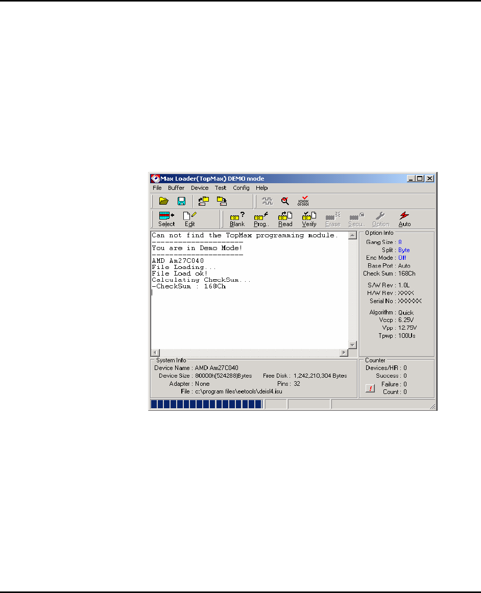
Proview User’s Guide
63
Be sure power cord is securely attached to programmer and power pack to
wall socket.
Be sure that power switch is ON.
Be sure that the USB cable is correctly and securely attached to the
programmer and PC. The connection must be direct; there cannot be any
software keys or locks between the USB port and the programmer. Most
switch boxes may also cause difficulties.
You may need to change your USB port because SpeedPRO/SpeedPRO
800(400)/SpeedPRO S800(S400) communicates with your computer via the
USB port in a bi-directional mode.
USB port set up for “ CANNOT FIND PROGRAMMING MODULE” in
ProView
5. Calling Customer Support
Compass Systems provides telephone technical assistance during normal
business hours (9:00 AM to 5:00 PM).
Please call our Technical Support Department or your local Compass
Systems’ distributor while you are at your computer and be prepared to
repeat the sequence of steps leading up to the problem
Have the following information ready when you call:

Proview User’s Guide
64
- The invoice number for the user who bought SpeedPRO, SpeedPRO
800(400) and SpeedPRO S800(S400) from Compass Systems.
- The distributor's name and the purchased date.
- The model & serial number found in the posterior side of the
Programming module.
- Your hardware software revision number from the option info screen.
- Description of problem with error message.
- The exact part number you are working with.
6. Service Information
Before sending a unit in for service, call us at Compass Systems to
obtain a Return Authorization Number (RMA). We will not repair
your unit unless an RMA was issued.
Warranty Service: Please return the product in the original package
with proof of purchase to the below address. Clearly state in writing the
performance problem and send any leads, connectors and accessories
that you are using with the device.
Non-Warranty Service: Return the product in the original packaging to the
below address. Clearly state in writing the performance problem and return any
leads, connectors and accessories that you are using with the device. Customers
not on open account must include payment in the form of a money order or credit
card. For the most current repair charges contact the factory before shipping the
product.
Return all merchandise to Compass Systems, Inc., with pre-paid shipping.
The flat-fee repair charge includes return ground shipping to addresses in South
Korea only. For overnight shipments and non-South Korea shipping fees contact
Compass Systems, Inc.
Compass Systems, Inc.
1403 ACE Techno Tower 8, 191-7, Kuro-Dong, Kuro-Gu
Seoul, Korea.
www.Compass21.com
Tel : +82-2-2109-8660
Fax : +82-2-2109-8661
Include with the instrument your complete return shipping address, contact
name, phone number, and description of problem.

Proview User’s Guide
65
7. Limited One-Year Warranty
Compass Systems, Inc., warrants to the original purchaser that its product and the
component parts thereof, will be free from defects in workmanship and materials
for a period of one year from the date of purchase.
Compass Systems, Inc., will, without charge, repair or replace, at its option,
defective products or component parts. Returned products must be accompanied
by proof of the purchase date in the form of a sales receipt.
To obtain warranty coverage in the South Korea, this product must be
registered by completing and mailing the enclosed warranty card to:
Compass Systems, Inc., 1403 ACE Techno Tower 8, 191-7, Kuro-Dong, Kuro-
Gu, Seoul, Korea. Within fifteen (15) days from proof of purchase
Exclusions: This warranty does not apply in the event of misuse or abuse of
the product or as a result of unauthorized alterations or repairs. It is void if
the serial number is alternated, defeated, or removed.
Compass Systems, Inc. shall not be liable for any consequential damages,
including without limitations to damages resulting from loss of use. Some states
do not allow limitation of incidental or consequential damages, so the above
limitation or exclusion may not apply to you.
This warranty gives you specific rights and you may have other rights, which
vary from state-to-state.
Model Number:___________________ Date Purchased:______________
8. Useful Web Site Addresses/ Phone Numbers
Compass Systems… ………www.compass21.com
E.E. Tools………… ………www.eetools.com
ALTERA ..............................www.altera.com
AMD.....................................www.amd.com
INTEL................................... www.intel.com
ATMEL ................................www.atmel.com
CYPRESS.............................www.cypress.com
DALLAS SEMI....................www.dalsemi.com
HITACHI..............................www.halsp.hitachi.com
INTEL...................................www.intel.com
ISSI .......................................www.issi.com
LATTICE SEMI. .................www.latticesemi.com
MITSUBISHI .......................www.mitsubishi.com

Proview User’s Guide
66
MICROCHIP ........................ www.microchip.com
MOTOROLA........................www.motorola.com
NATIONAL SEMI. ..............www.national.com
NEC ......................................www.nec.com
OKI SEMI.............................www.okisemiconductor.com
PHILIPS SEMI. ....................www.semiconductors.philips.com
ROHM ..................................www.rohm.com
SEEQ ....................................www.seeq.com
SILICON STORAGE ...........www.ssti.com
ST MICRO ...........................www.st.com
TEMIC..................................www.temic.com
T.I. ........................................www.ti.com
TOSHIBA.............................www.toshiba.com
WAFERSCALE....................www.waferscale.com
WINBOND...........................www.winbond.com
XICOR..................................www.xicor.com
XILINX ................................www.xilinx.com
ZILOG ..................................www.zilog.com
9. Programming Adapter Manufacturers
Compass Systems(Asia). .....www.compass21.com
E.E. Tools(USA)……….……www.eetools.com
Emulation Technology..........www.1800adapter.com
Emulation Solutions..............www.adapters.com
Logical System .....................www.logicalsys
Iron Wood.............................www.ironwoodelectronics.com
10. EPROM Emulator Manufacturers
E.E. Tools……………………www.eetools.com
Tech Tools ............................www.tech-tools.com

Proview User’s Guide
67
8. GLOSSARY
BGA Ball Grid Array. A surface mount device with solder balls
and a high pin count, similar to PGA.
Bipolar PROM A fuse-link programmable PROM.
Blank Check A test performed by a device programmer to ascertain
whether a device has been programmed (partial or total)
or is in a virgin state.
Buffer Data storage unit directly stored on CPU.
Checksum A number that results by adding up every element of a
pattern. Typically either a four or eight digit HEX number,
it is a quick way to identify a pattern, since it is very
unlikely that two patterns will have the same checksum.
Compare Reading a programmable device and displaying any
discrepancies from the desired pattern. Each error is
displayed on the screen. This comparison is slower to
perform than a verify on the programmer.
Device Microchip or Integrated Circuit chip.
Die The silicon chip that is located within an IC package. It is
a small rectangular flat piece of silicon that has been
fabricated with many transistors to perform a specific
function. It is glued into a plastic or ceramic package and
connected to the external metal interconnect pins of the IC
with very small bonding wires. It can be seen through the
window of erasable EPROMs.
DIP Dual Inline Package. An IC package with two rows of
through-hole pins, usually on 0.1 pitch, 0.3 or 0.6 inches
apart.
FPGA Field Programmable Gate Array. A very complex PLD.
The FPGA usually has an architecture that comprises a
large number of simple logic blocks, a number of
input/output pads, and a method to make random
connections between the elements.
Functional Test A test that is performed following the programming of a
PLD. The test operates the device in its normal operating
mode by simulating the inputs and outputs that the part
will experience in normal operation. To perform the test,
the engineer must supply a set of test vectors that describe
normal operation of the device so the device programmer
can apply the specified stimulus and verify that the device
is operating as designed. It is important to perform a
functional test on PLDs because, in many cases, the PLD
cannot be fully tested at the factory before programming
so a defective PLD may program correctly but fail the
functional test. A properly designed functional test will
verify that the part meets the design specification,
ensuring that the device, the compiler, the programmer,

Proview User’s Guide
68
and the engineer have all performed their respective tasks
correctly.
Fuse A metal connection within a PLD or memory that may be
melted during programming to break the circuit. These
links typically carry input signals to logic gates. Burning
all the fuses except those that are required in the desired
circuit forms the desired circuit configuration. Since the
fuses cannot be tested nondestructively, fuse-like
programmable devices cannot be 100% tested at the
factory and consequently expected programming yields
are usually 98-99%.
GAL Generic Array Logic. EEPROM based second generation
PAL devices.
Gang Programmer A multiple-socket programmer that requires each device
to be placed in a socket before any can be programmed.
See Concurrent Programmer.
HEX file A human-readable ASCII file that represents any binary
data. Each byte in the binary pattern is represented by two
HEX characters (0-9, A-F) so that any of the 256 possible
bytes, which include both control and unprintable
characters, may be printed. The HEX file may also contain
address or checksum information. The pattern represented
by the HEX file may be represented by a binary file or any
of the HEX file formats – any file format may contain any
pattern. The names of the HEX file formats (Intel,
Motorola, Tektronix, etc.) indicate who standardized its
format and does not indicate anything about the pattern or
the device the pattern is intended for.
I/O Input/ Output.
JEDEC Joint Electron Device Engineering Council (pronounced
JED’eck). A group organized by the IEEE (Institute of
Electrical and Electronics Engineers) that has defined a
standard file format for PLDs.
JEDEC file A file conforming to a standard format that specifies the
configuration and testing procedure for a PLD. The file is
in a human-readable ASCII format and consists of fields
that start with a letter and end with an asterisk. Fields
specify the pattern to program into the part, whether to
secure the device, a set of test vectors to perform a
functional test, and checksums to verify the integrity of
the file.
LCC Leadless Chip Carrier. A square ceramic package that has
no leads; Instead it has metal areas that are surface-
mount soldered to the target circuit. This package is
usually used only for military and aerospace applications.
Available up to 84 pins.

Proview User’s Guide
69
Memory device A Device that contains an array of storage locations. The
device has a set of inputs, called address, which specify
which location in the array is being accessed. A set of
input/output pins produce the stored number (pattern)
when the device is read, and accept a new value when
the device is written or programmed. Additionally, there
are one or more input pins that select the operating move
(read, write, standby, etc.). Memory devices may be
classified by whether they are volatile or nonvolatile, and
whether they may be erased. The memory’s organization
refers to its word width and the number of words in the
device.
Microcontroller A device that contains a central processing unit (CPU),
memory, and I/O ports on a single IC. Microcontrollers
that contain any form of nonvolatile memory may be
programmed on a device programmer. When connected
to a power supply and external crystal, many of these
devices form a complete microcomputer.
Non-Volatile The Characteristic of a memory that does not lose its
contents when its power is removed. Non-volatile
memory is useful in microcomputer circuits because it
can provide instructions for a CPU as soon as the power
is applied, before secondary devices, such as disk, can be
accessed. Non-Volatile memory includes ROM, EPROM
and EEPROM.
Oscillator A device that produces an alternating output current.
OTP One-time programmable. The characteristic of a memory
device that can be programmed once but cannot be
erased. When an EPROM is described as OTP, this
means that its die is erasable when exposed to ultraviolet
light, but because of its package, which is not transparent,
it cannot be exposed to light and thus it cannot be erased.
Package The plastic or ceramic that protects an IC die and
connects it to the target circuit.
Parallel printer port A standard port on virtually every PC designed for
connection to a printer. This port has eight data lines and
several control lines. Parallel ports may be either
unidirectional or bi-directional. If your computer has a
unidirectional port, the programmer will use the status
lines to read data back from the programmer. The port
allows high-speed communication (many times faster
than a serial port). There may be up to three parallel
ports in most PCs designated LPT1, LPT2, and LPT3.
PGA Pin Grid Array. A square, through-hold IC package that
has pins located on a square grid with 0.1000-inch pitch.
It may have up to several hundred pins. Used primarily
for military and prototype designs.

Proview User’s Guide
70
PLCC Plastic Leaded Chip Carrier, A square plastic package
that has J-shaped leads on four sides. This can be
surface mounted or placed in a socket for through-hole
use. Available in 20 to 84 pins.
PLD Compiler A software package that allows an engineer to specify
the functionality of a PLD through a high-level
language or schematic diagram. The software will
convert the design into a JEDEC or other file for the
PLD programmer. PLD compilers are available from
numerous IC manufacturers and from third parties. The
packages from IC manufacturers support only one
brand of device and may be free, inexpensive or
expensive. The most popular compiler is PALASM
(prices under $200, available from AMD sales offices
and representatives), which supports most of AMD’s
line of PLDs with an easy-to-learn high-level language.
The compiler that probably offers the highest level of
functionality and flexibility is PLDmaster made by
Logical Devices. It supports most PLDs and offers a
sophisticated input language with full support for state
machines and other complex constructs, partitioning
designs into several PLDs, and graphical input. Their
tools run on PCs and workstations. PLD compilers have
simulators that can be used to test the functionality of
your design and validate test vectors that you design
before programming a device.
PQFP Plastic Quad Flat Pack. See QFP.
QFP Quad Flat Pack. A square IC package that has surface-
mount leads coming from four sides. It is used for high-
density applications, usually over 100 pins. Lead pitch
may be 0.025 inches or smaller.
RAM Random Access Memory. A volatile memory device.
ROM Read Only Memory. A non-volatile memory device
that cannot be programmed by the user. It is
programmed at the factory through the use of a mask
pattern in the final fabrication steps of the die.
Serial Memory An EPROM or EEPROM that is accessed by shifting
in addresses and shifting out data one bit at a time.
Interfaces are available using one, two or three wires
for clock, data in, and data out.
Socket module An interchangeable metal chassis that contains a
programming socket.
SOIC Small Outline Integrated Circuit. A surface-mount IC
package that has two rows of leads on opposite sides.
Commonly found in 8 to 32 pin sizes. Leads are
usually 0.050 pitch.

Proview User’s Guide
71
Test vector A set of characters that describe the inputs and outputs
of a device during a functional test. There is one
character in the vector for each pin on the device.
Numbers represent inputs to be applied to the device
(1 for Vih, 0 for Vil). Letters represent the outputs that
must be tested (H for Voh, L for Vol, Z for high-
impedance). During the test, the part will be powered
up and each input will be applied to the device for the
first vector. Then, each output will be applied to the
device for the first vector. This process will continue
for each vector and any errors will be reported.
TQF Thin Quad Flat Pack. Similar to QFP but with a lower
profile and physically smaller in length and width.
TSOP Thin Small Outline Package. A surface-mount
package with fine-pitch leads (usually 0.025 inch
pitch) on two sides. This package is very low profile
and commonly available in a reverse (mirror image)
pinout used to simplify circuit board layout. Usually
32 to 44 pins.
UV Erasable The characteristic of an EPROM that allows it to be
erased with exposure to short –wave ultra-violet light.
This high-energy light can discharge the floating-gate
transistor cells that store bits in an EPROM. The most
common source of such light is a mercury vapor tube
much like an ordinary fluorescent tube, but without
the phosphor that turns the UV light emitted by the
mercury into visible light. The light from ordinary
fluorescent lamps or sunlight generally takes years to
erase an EPROM. All UV erasable parts have a quartz
windowed ceramic package that allows exposure with
UV light.
Verify Reading a programmable device and comparing its
contents to the desired pattern for that device. This is
a go/no-go test – it does not report what the
discrepancies are. See also: compare.
Word width The number of output pins that a memory device has.
The most common size for EPROMs is byte wide (8
bits) and “word” wide, or 16 bits. It can also refer to
the aggregate width of several memory devices used
in a set.
PLA Programmable Logic Array: Programmable AND
array feeding a fixed OR array
GAL Generic Array Logic
MACH high density PLD

Proview User’s Guide
72
PLD Programmable Logic Device
CPLD Complex PLD
PROM Programmable Read Only Memory
EPROM Erasable PROM
EEPROM Electrically Erasable PROM