Computime CT-EM2531 Zigbee Module User Manual ZigBee Ready RF Transceiver Modules
Computime Limited Zigbee Module ZigBee Ready RF Transceiver Modules
User Manual


EM2531/01 ZigBee- Ready RF Transceiver Modules
All rights reserved. Property of Computime Ltd. 2 / 13 V1.0
TABLE OF CONTENTS
GENERAL DESCRIPTION ..........................................................................1
Applications................................................................................................. 1
Features....................................................................................................... 1
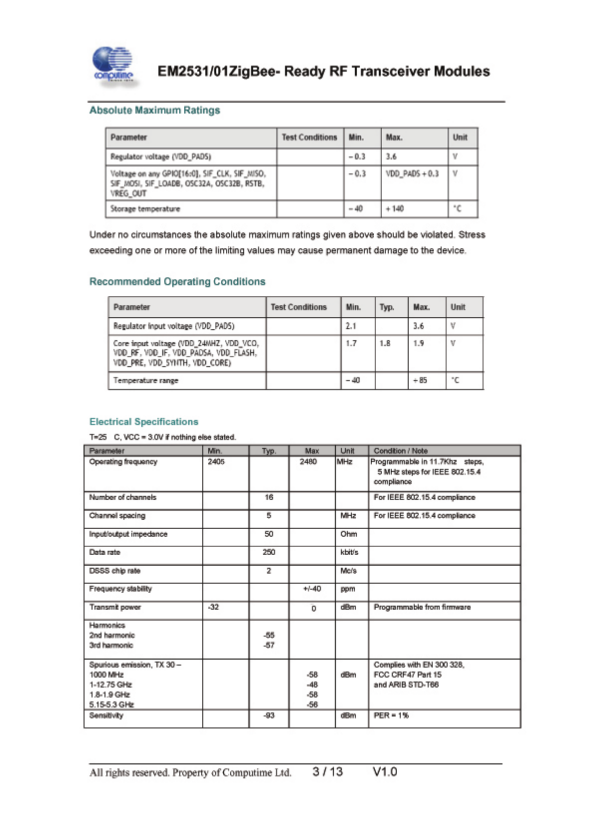
Absolute Maximum Ratings.......................................................................... 3
Recommended Operating Conditions………….………………………………3
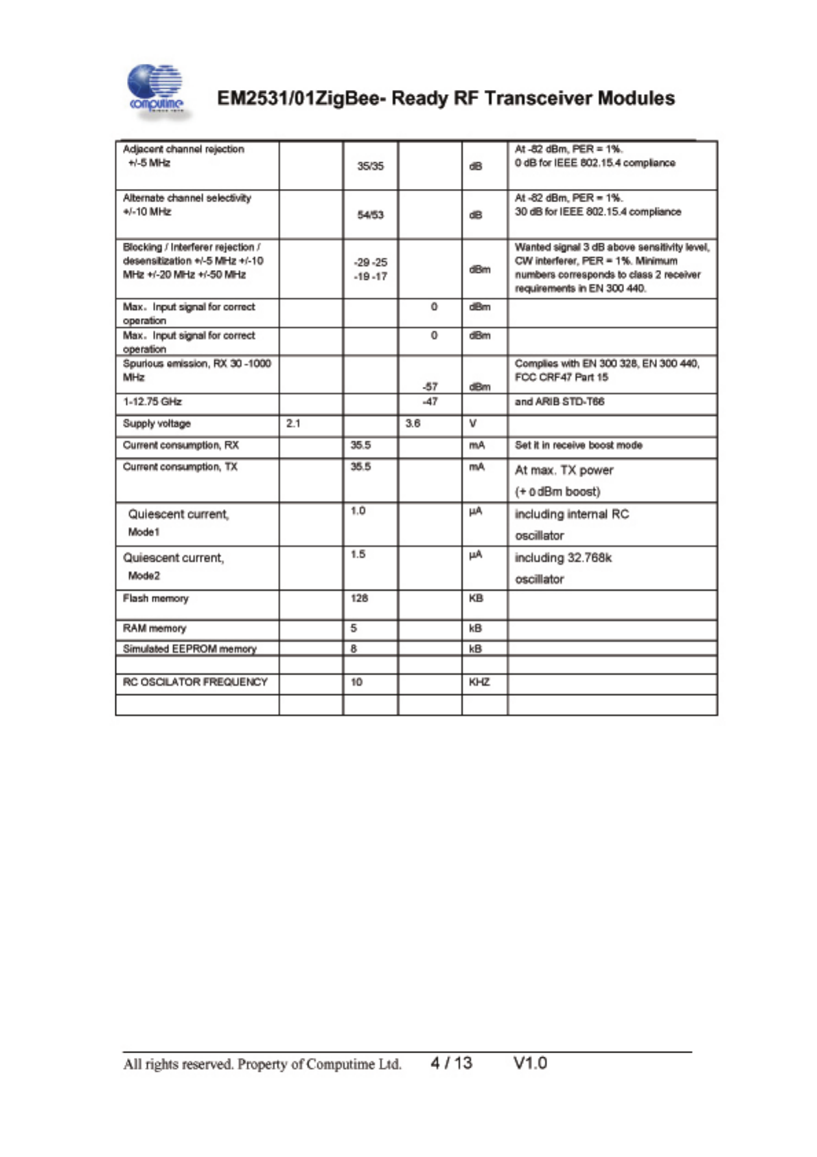
Electrical Specifications.................................................................................3
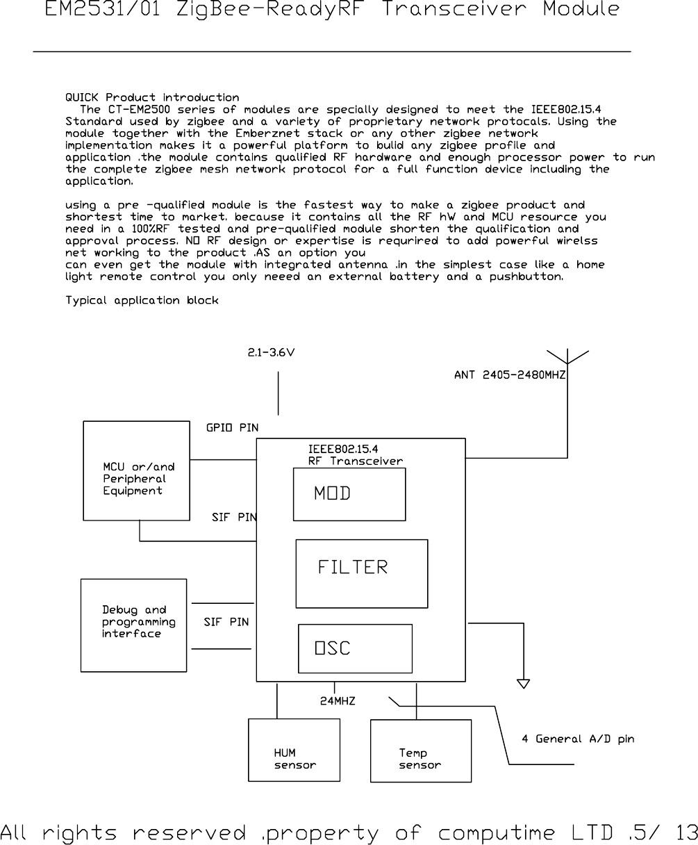
Quick Product Introduction.................................. ........................................ 5
Typical application circuit...............................................................................5
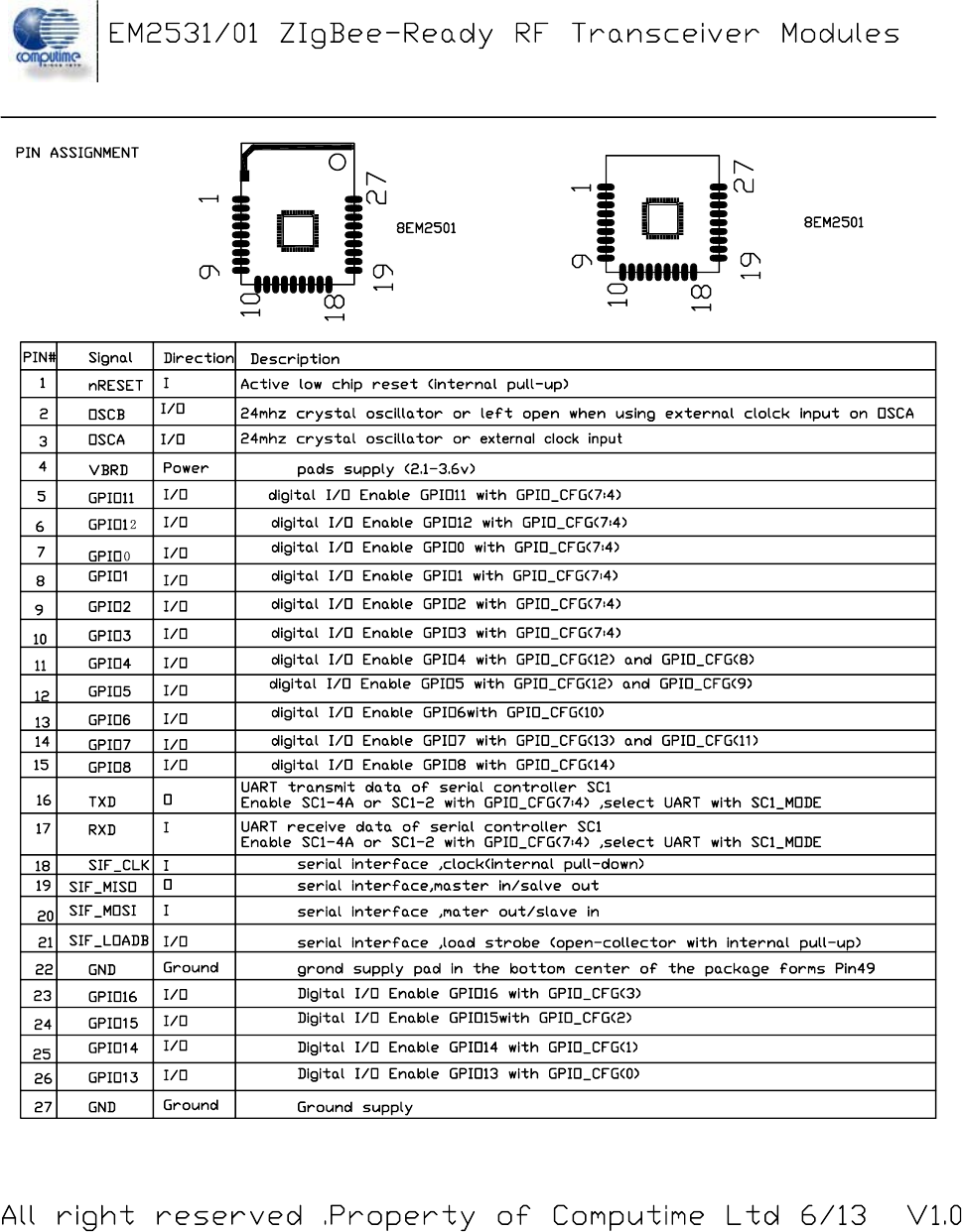
Pin Assignment..............................................................................................6
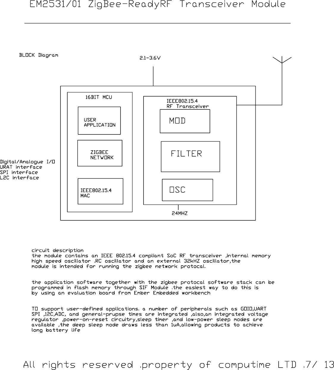
Block Diagram...............................................................................................7
Circuit Description ........................................................................................7
SIF Module Programming and Debug Interface...........................................8
Power Management.....................................................................................8
RF Frequency, Output Power Levels and Data Rates.................................9
PCB Layout Recommendations................................................................ 12
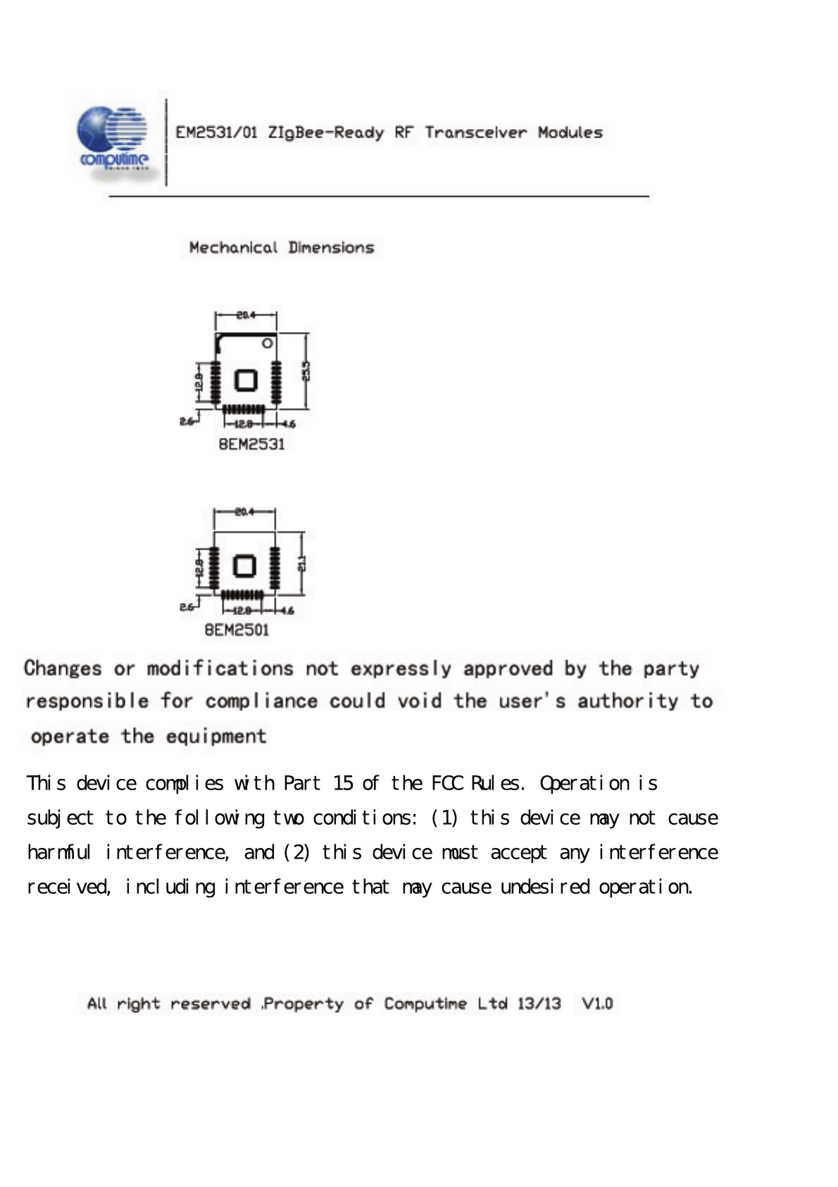
Mechanical Dimensions..............................................................................13

EM2531/01 ZigBee- Ready RF Transceiver Modules
All rights reserved. Property of Computime Ltd. 8 / 13 V1.0
SIF Module Programming and Debug Interface
SIF is a synchronous serial interface developed by Cambridge Consultants Ltd. It is
the primary programming and debug interface of the CT-EM2500. The SIF module
allows external devices to read and write memory-mapped registers in real-time
without changing the functionality or timing of the XAP2b core.
The SIF interface provides the following:
z IC production test (especially analog)
z PCB production test
z XAP2b code development
z Product control and characterization
The pins are:
z SIF_LOADB
z SIF_CLK
z SIF_MOSI
z SIF_MISO
The maximum serial shift speed for the SIF interface is 48MHz. SIF interface
accesses can be initiated even when the chip is in idle and deep sleep modes. An
edge on SIF_LOADB wakes the chip to allow SIF cycles.
Power Management
The CT-EM2500 supports three different power modes: processor ACTIVE,
processor IDLE, and DEEP SLEEP.
The IDLE power mode stops code execution of the XAP2b until any interrupt occurs
or an external SIF wakeup command is seen. All peripherals including the radio
continue to operate normally.
The DEEP SLEEP power mode powers off most of the module but leaves the critical
chip functions, such as the GPIO pads and RAM powered by the High Voltage Supply
(VDD_PADS). The module can be woken by configuring the sleep timer to generate
an interrupt after a period of time, using an external interrupt, or with the SIF interface.
Activity on a serial interface may also be configured to wake the module, though
actual reception of data is not re-enabled until the module has finished waking up.
Depending on the speed of the serial data, it is possible to finish waking up in the
middle of a byte. Care must be taken to reset the serial interface between bytes and
discard any garbage data before the rest. Another condition for wakeup is general
activity on GPIO pins.

EM2531/01 ZigBee- Ready RF Transceiver Modules
RF Frequency, Output Power Levels and Data Rates
The following table shows the RF channels as defined by the IEEE 802.15.4 standard.
For proprietary solutions (non-IEEE 802.15.4), the RF transceiver can be
programmed in resolution of 11.7 KHZ.
The output power level can be configured from the firmware in the range -32 to 5 dBm.
The RF transceiver uses direct sequence spread spectrum (DSSS) with 2 Mchip/s
chip rate, giving a raw data rate of 250 kbit/s. The modulation format is Offset –
Quadrature Phase Shift Keying (O-QPSK). The DSSS makes the communication link
robust in noisy environments when sharing the same frequency band with other
applications.
The use of RF frequencies and maximum allowed RF power is limited by national
regulations. The CT-EM2500 is complying with the applicable regulations for the
world wide 2.45 GHz ISM band.
Specifically it complies with the European Union R&TTE directive meeting EN 300
328 . It also meets the FCC CFR47 Part15 regulations for use
in the US and the ARIB T-66 for use in Japan.
All rights reserved. Property of Computime Ltd. 9 / 13 V1.0
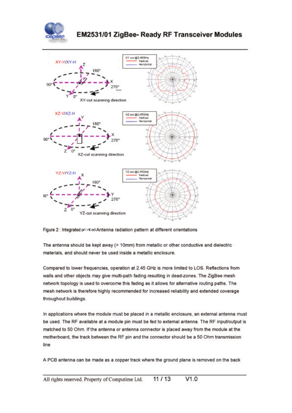
printed
EM2531/01 ZigBee- Ready RF Transceiver Modules
side. The rest of the PCB board should have a ground plane as large as possible, preferably as
large (in one dimension) as the antenna itself, to make it act as a a reflector mirror to the antenna. A
quarter wavelength Antenna on a PCB must be shorter than the wire antenna due to the influence
of the dielectric material of the PCB. The length reduction depends on the PCB thickness and
material, as well as how close to the edge of the board the antenna is placed. Typical reduction is to
75-90 % but must be found empirically.
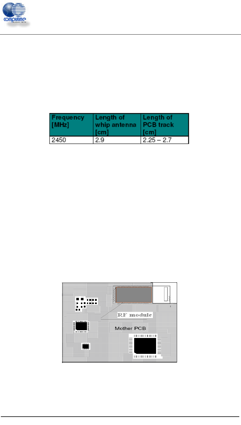
The length of a quarter-wave antenna is given in the table below.
If, for space reasons, the track is made even shorter than the resonating quarter of wavelength, the
antenna should be matched to 50 ohms using a series inductor and a shunt capacitor.
PCB Layout Recommendations
For recommended layout pads for the module, please reference Mechanical Dimensions
The area underneath the module should be covered with solder resist in order to prevent short
circuiting the test pads on the back side of the module. A solid ground plane is preferred.
Unconnected pins should be soldered to the pads, and the pads should be left floating. For the
module version with integrated antenna, the RF pad can be soldered, but the pad should not be
connected further. The two ground pads (pin 10 should be grounded for all variants.)
When using the onboard chip antenna, careful attention is required to the layout of the PCB where
the module is mounted. In Figure 3 a mother PCB is shown with a recommended placement of the
module.
Figure 3 A recommended placement of the module on a mother PCB (Shaded area is
ground-plane on mother PCB)
All rights reserved. Property of Computime Ltd. 12 / 13 V1.0
This device complies with Part 15 of the FCC Rules. Operation is
subject to the following two conditions: (1) this device may not cause
harmful interference, and (2) this device must accept any interference
received, including interference that may cause undesired operation.