Computime CTL3579A ZigBee Module User Manual
Computime Limited ZigBee Module
Users Manual

Copyright © 2011 Computime Limited. All rights reserved. Rev. 2
ZigBee-Ready RF Transceiver Module
(IEEE 802.15.4)
CTL3576/7/8/9
The reproduction of this datasheet is NOT allowed without approval of Computime Limited. All information and data
contained in this datasheet are subject to change without notice. This publication supersedes and replaces all information
previously supplied. Computime has no responsibility to the consequence of using the information described in this
document.

ZigBee- Ready RF Transceiver Module CTL3576/7/8/9
Copyright © 2011 Computime Limited. All rights reserved. Rev. 2
Revision
Rev. Date
(DD-MM-YYYY)
History
1 18-09-2011
First Release

ZigBee- Ready RF Transceiver Module CTL3576/7/8/9
Copyright © 2011 Computime Limited. All rights reserved. Rev.2
Table of Contents
1. General Description...................................................................................................................................... 0
2. Applications .................................................................................................................................................. 0
3. Features ....................................................................................................................................................... 0
4. Absolute Maximum Ratings.......................................................................................................................... 1
5. Recommended Operating Conditions .......................................................................................................... 1
6. Electrical Specifications................................................................................................................................ 1
7. Typical application block .............................................................................................................................. 3
8. Pin Assignment............................................................................................................................................. 3
9. Pin Description ............................................................................................................................................. 4
10. Block Diagram......................................................................................................................................... 11
11. RF Frequency Detail............................................................................................................................... 12
12. PCB Layout Recommendations.............................................................................................................. 13
13. Mechanical Dimensions.......................................................................................................................... 14
14. Modules Differentia................................................................................................................................. 15

ZigBee- Ready RF Transceiver Module CTL3576/7/8/9
Copyright © 2011 Computime Limited. All rights reserved. Rev. 1
1. General
Description
The CTL357x RF Transceiver Module is compact surface mounted Module specially designed for
Ember ZigBee™ protocol stack for wireless networks, EmberZNet, based on IEEE 802.15.4
standard in the 2.4GHz world-wide ISM band. The complete module is only 32.4 x 25.4 x 4.1 mm. It
integrated a 2.4GHz, IEEE 802.15.4-2003 compliant transceiver with a 32-bit network processor
(ARM Cortex-M3 Processor) to run EmberZNet. They contain embedded Flash and integrated RAM
for program and data storage. It utilizes the non-intrusive SIF module for powerful software
debugging and programming of the network processor.
2. Applications
Home
automation &
building control
Home
appliances &
alarms
Monitoring of
remote
systems
Security
systems &
lighting
controls
Sensor data
capture in
embedded
networks
3. Features
Complete ZigBee-ready module with integrated PCB antenna
Integrated IEEE 802.15.4 PHY and MAC layer
Non-intrusive debug interface (SIF)
SPI interface for communication and controlled by the Host using the EmberZNet Serial Protocol
(EZSP)
Internal RC oscillator for timer
High performance direct sequence spread spectrum (DSSS) RF transceiver
16 channels in the 2.4 GHz ISM band
On-chip regulator for 2.1-3.6V operation , three sleep low power modes
32-bit ARM® Cortex™-M3 processor
192KB FLASH ROM and 12KB RAM(EM357 internal) ,8Mb off chip Flash memory
(CTL3577&CTL3579)
+20dBm transmission power
-98dBm excellent reception sensitivity. (Boost mode -101dBm)
Small footprint: 32.4 x 25.4 x 4.1 mm
Optional MMCX connector for external antenna
Extremely low Deep Sleep Current.
ZigBee- Ready RF Transceiver Module CTL3576/7/8/9
Copyright © 2011 Computime Limited. All rights reserved. Rev. 1
4. Absolute
Maximum Ratings
Parameter Test Conditions Min. Max. Unit
Regulator input voltage (VDD_PADS) -0.3 +3.6
V
RF Input Power
(for max level for correct packet reception)
RX signal into a lossless balun +15 dBm
Voltage on any GPIO (PA[7:0], PB[7:0],
PC[7:0]), SWCLK, nRESET,
VREG_OUT
-0.3 VDD_PADS
+0.3
V
Voltage on any GPIO pin (PA4, PA5, PB5,
PB6, PB7, PC1), when used as an input to the
general purpose ADC with the low voltage
range selected
-0.3 2.0
V
Voltage on OSCA, OSCB, NC -0.3 VDD_PADSA
+0.3
V
Storage temperature -40 +140 °C
5. Recommended Operating Conditions
Parameter Test Conditions Min. Typ. Max. Unit
Regulator input voltage (VDD_PADS) 2.7
3.6 V
Operating temperature range 0 +70①°C
6. Electrical
Specifications
T=25℃, VCC = 3.0V, Fo =2450MHZ, if nothing else stated.
Parameter Condition / Note Min Typ. Max Unit
Operating frequency Programmable in 5MHz steps, 5 MHz
steps for IEEE 802.15.4 compliance 2.4 2.5 GHz
Number of channels For IEEE 802.15.4 compliance 16
Channel spacing For IEEE 802.15.4 compliance 5 MHz
Input/output impedance 50 Ohm
Frequency stability +/-40 ppm
Transmit power Programmable from firmware -15 +20 dBm
① Operationg temperature range from -40 to 85°C for module CTL3576 and CTL3578.
ZigBee- Ready RF Transceiver Module CTL3576/7/8/9
Copyright © 2011 Computime Limited. All rights reserved. Rev. 1
Parameter Condition / Note Min Typ. Max Unit
Sensitivity
PER = 1% PER, 20byte packet
defined by IEEE 802.15.4 Boost
mode
-98 dBm
Adjacent channel rejection +/-5 MHz IEEE 802.15.4 compliance at -82
dBm 35/35 dB
Adjacent channel rejection +/-10 MHz IEEE 802.15.4 compliance at -82
dBm 40/40 dB
Co-channel rejection -6 dB
Supply voltage 2.7 3.6 V
Max RX sensitivity (normal mode) 28 mA
Current consumption,
RX mode Max RX sensitivity (boost mode) 30 mA
Current consumption,
TX mode 190 mA
Deep sleep current 10② μA
Flash Memory 192③ KB
MCU clock frequency 24 MHz
② Deep sleep current less than 5 uA for module CTL3576 and CTL3578.
③ Only CTL3577 and CTL3579 have 8Mb off chip flash memory on the RF module.
ZigBee- Ready RF Transceiver Module CTL3576/7/8/9
Copyright © 2011 Computime Limited. All rights reserved. Rev. 1
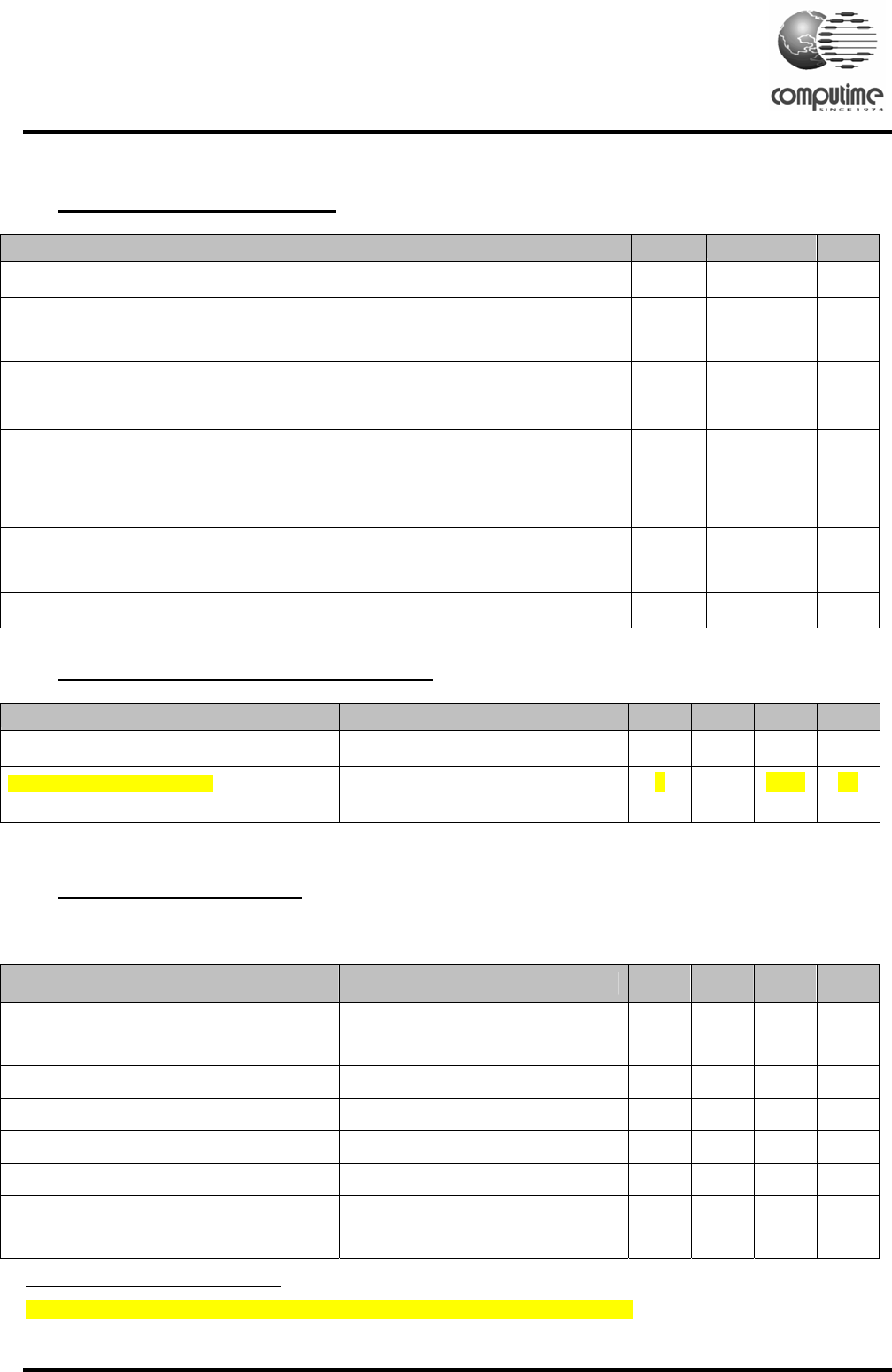
7. Typical application block
Figure 1: Example of application circuit
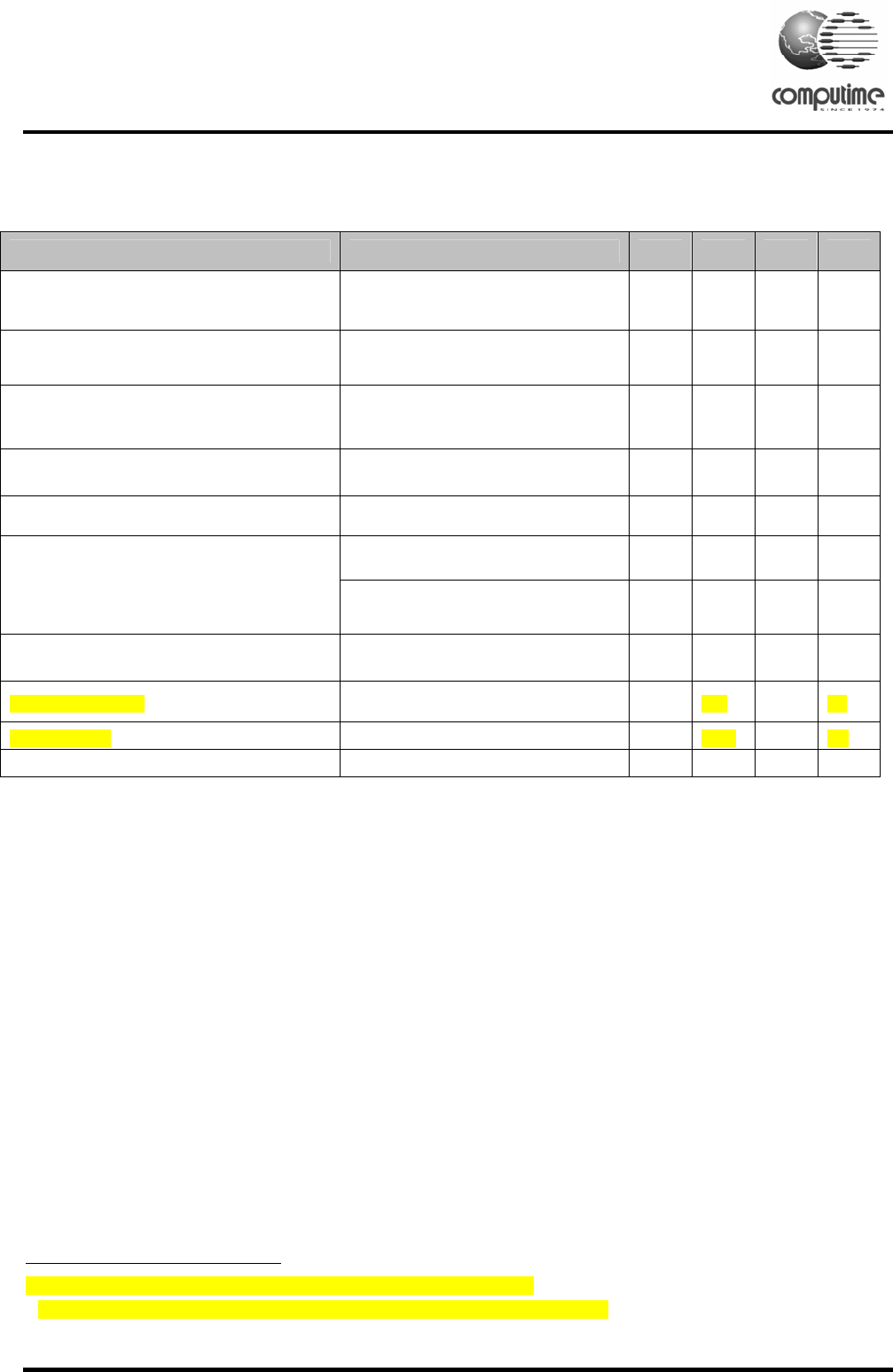
8. Pin
Assignment
Figure 2: CTL357x pin assignment
CTL357x
RF Module
VDD_PADS=2.7- 3.6V
Debug and
programming
interface
HOST
MCU
NREST
PTI_EN
PTI-DATA
SIF_CLK
SIF-MISO
SIF-MOSI
NSIF LOAD
LINK_ACTIVITY
8Mb flash32.768kHz
24MHz

ZigBee- Ready RF Transceiver Module CTL3576/7/8/9
Copyright © 2011 Computime Limited. All rights reserved. Rev. 1
9. Pin
Description
Pin# CTL3576 CTL3577 CTL3578 CTL3579 Direction Description
JTCK JTCK JTCK JTCK I
JTAG clock input from
debugger
1
SWCLK SWCLK SWCLK SWCLK I/O
Serial Wire Clock input/output
with debugger
PC2 PC2 PC2 PC2 I/O
Digital I/O Enable with
GPIO_DBGCFG[5]
JTDO JTDO JTDO JTDO O JTAG data out to debugger
2
SWO SWO SWO SWO O
Serial Wire Output
asynchronous trace output to
PC3 PC3 PC3 PC3 I/O
Digital I/O Enable with
GPIO_DBGCFG[5]
3
JTDI JTDI JTDI JTDI I JTAG data in from debugger
PC4 PC4 PC4 PC4 I/O
Digital I/O Either Enable with
GPIO_DBGCFG[5]
JTMS JTMS JTMS JTMS I
JTAG mode select from
debugger
4
SWDIO SWDIO SWDIO SWDIO I/O
Serial Wire bidirectional data
to/from debugger
PC0 PC0 PC0 PC0
I/O High
current
Digital I/O Either Enable with
GPIO_DBGCFG[5]
JRST JRST JRST JRST I JTAG reset input from
debugger
IRQD IRQD IRQD IRQD I
Default external interrupt
source D
5
TRACEDATA1 TRACEDATA1 TRACEDATA1 TRACEDATA1 O Synchronous CPU trace data
bit 1
PB7 PB7 PB7 PB7
I/OHigh
current Digital I/O
6
ADC2 ADC2 ADC2 ADC2 Analog ADC input 2

ZigBee- Ready RF Transceiver Module CTL3576/7/8/9
Copyright © 2011 Computime Limited. All rights reserved. Rev. 1
IRQC IRQC IRQC IRQC I
Default external interrupt
source C
TIM1C2 TIM1C2 TIM1C2 TIM1C2 O Timer 1 channel 2 output
TIM1C2 TIM1C2 TIM1C2 TIM1C2 1 Timer 1 channel 2 input
PB6 PB6 PB6 PB6
I/O High
current Digital I/O
ADC1 ADC1 ADC1 ADC1 Analog ADC input 1
IRQB IRQB IRQB IRQB I External interrupt source B
TIM1C1 TIM1C1 TIM1C1 TIM1C1 O Timer 1 channel 1 output
7
TIM1C1 TIM1C1 TIM1C1 TIM1C1 I Timer 1 channel 1 input
Pin# CTL3576 CTL3577 CTL3578 CTL3579 Direction Description
PA7 PA7 PA7 PA7
I/O High
current
Digital I/O Disable REG_EN
with GPIO_DBGCFG [4]
TIM1C4 TIM1C4 TIM1C4 TIM1C4 O Timer 1 channel 4 output
TIM1C4 TIM1C4 TIM1C4 TIM1C4 I Timer 1 channel 4 input
8
REG_EN REG_EN REG_EN REG_EN O External regulator open drain
output
PC1 PC1 PC1 PC1 I/O Digital I/O
ADC3 ADC3 ADC3 ADC3
Analog ADC input 3
SWO SWO SWO SWO O
Serial Wire Output
asynchronous trace output to
9
TRACEDATA0 TRACEDATA0 TRACEDATA0 TRACEDATA0 O Synchronous CPU trace data
bit 0
10
GND GND GND GND

ZigBee- Ready RF Transceiver Module CTL3576/7/8/9
Copyright © 2011 Computime Limited. All rights reserved. Rev. 1
PB3 PB3 PB3 PB3 I/O
Digital I/O
TIM2C3 TIM2C3 TIM2C3 TIM2C3 O Timer 2 channel 3 output
TIM2C3 TIM2C3 TIM2C3 TIM2C3 I Timer 2 channel 3 input
SC1nCTS SC1nCTS SC1nCTS SC1nCTS I UART CTS handshake of
Serial Controller 1
SC1SCLK SC1SCLK SC1SCLK SC1SCLK O SPI master clock of serial
Controller 1
11
SC1SCLK SC1SCLK SC1SCLK SC1SCLK I SPI slave clock of serial
Controller 1
12
GND GND GND GND
PC6 PC6 PC6 PC6 I/O Digital I/O
OSC32B OSC32B I/O 32.768KHz crystal oscillator
13
NTX_ACTIVE NTX_ACTIVE NTX_ACTIVE NTX_ACTIVE O Inverted TX_ACTIVE signal
PC7 PC7 PC7 PC7 I/O
Digital I/O
OSC32A OSC32A I/O 32.768KHz crystal oscillator
14
OSC32_EXT OSC32_EXT OSC32_EXT OSC32_EXT I Digital 32.768KHz clock input
source
15
GND GND GND GND
16 VDD_PADS VDD_PADS VDD_PADS VDD_PADS Power Pads supply(2.1-3.6V)
17
nRESET nRESET nRESET nRESET I Active low chip reset(internal
pull-up)
Pin# CTL3576 CTL3577 CTL3578 CTL3579 Direction Description
18 PA0 PA0 PA0 PA0 I/O Digital I/O

ZigBee- Ready RF Transceiver Module CTL3576/7/8/9
Copyright © 2011 Computime Limited. All rights reserved. Rev. 1
TIM2C1 TIM2C1 TIM2C1 TIM2C1 O Timer 2 channel 1 output
TIM2C1 TIM2C1 TIM2C1 TIM2C1 I Timer 2 channel 1 input
SC2MOSI SC2MOSI SC2MOSI SC2MOSI O SPI master data out of serial controller
2
SC2MOSI SC2MOSI SC2MOSI SC2MOSI I SPI slave data in of serial controller 2
SI SI I
Serial data in fot the 8Mb flash④
PA1 PA1 PA1 PA1 I/O Digital I/O
TIM2C3 TIM2C3 TIM2C3 TIM2C3 O Timer 2 channel 3 output
TIM2C3 TIM2C3 TIM2C3 TIM2C3 I Timer 2 channel 3 input
SC2SDA SC2SDA SC2SDA SC2SDA I/O TWI data of serial controller 2
SC2MISO SC2MISO SC2MISO SC2MISO O SPI slave data out of serial controller 2
SC2MISO SC2MISO SC2MISO SC2MISO I SPI master data in of serial controller 2
19
SO SO O Serial data out of the 8Mb flash
PA2 PA2 PA2 PA2 I/O Digital I/O
TIM2C4 TIM2C4 TIM2C4 TIM2C4 O Timer 2 channel 4 output
TIM2C4 TIM2C4 TIM2C4 TIM2C4 I Timer 2 channel 4 input
SC2SCL SC2SCL SC2SCL SC2SCL I/O TWI clock of serial controller 2
20
SC2SCLK SC2SCLK SC2SCLK SC2SCLK O SPI master clock of serial controller 2
④ The SI,SO,SCK and CE# on the module pin18,19,20 and 23 are connected to the off chip 8Mbit SPI Serial
Flash(SST25VF080B).Details information about the flash memory ,refers to its datasheet. It applys to the module
CTL3577 and CTL3579.

ZigBee- Ready RF Transceiver Module CTL3576/7/8/9
Copyright © 2011 Computime Limited. All rights reserved. Rev. 1
SC2SCLK SC2SCLK SC2SCLK SC2SCLK I SPI slave clock of serial controller 2
SCK SCK I
Clock in for the 8Mb flash
PA6 PA6 PA6 PA6 I/O High
current Digital I/O
TIM1C3 TIM1C3 TIM1C3 TIM1C3 O Timer 1 channel 3 output
21
TIM1C3 TIM1C3 TIM1C3 TIM1C3 I Timer 1 channel 3 input
PB4 PB4 PB4 PB4 I/O Digital I/O
TIM2C4 TIM2C4 TIM2C4 TIM2C4 O Timer 2 channel 4 output
TIM2C4 TIM2C4 TIM2C4 TIM2C4 i Timer 2 channel 4 input
SC1nRTS SC1nRTS SC1nRTS SC1nRTS O UART RTS handshake of serial
controller 1
22
SC1nSSEL SC1nSSEL SC1nSSEL SC1nSSEL I SPI slave select of serial controller 1
Pin# CTL3576 CTL3577 CTL3578 CTL3579 Direction Description
PA3 PA3 PA3 PA3 I/O
Digital I/O
SC2Nssel SC2Nssel SC2Nssel SC2Nssel I SPI slave select of serial
controller 2
TRACECLK TRACECLK TRACECLK TRACECLK O Synchronous CPU trace
clock
TIM2C2 TIM2C2 TIM2C2 TIM2C2 O Timer 2 channel 2 output
TIM2C2 TIM2C2 TIM2C2 TIM2C2 I Timer 2 channel 2 input
23
CE# CE# I
Chip Enable for the 8Mb flash
24 PA4 PA4 PA4 PA4 I/O
Digital I/O

ZigBee- Ready RF Transceiver Module CTL3576/7/8/9
Copyright © 2011 Computime Limited. All rights reserved. Rev. 1
ADC4 ADC4 ADC4 ADC4 Analog ADC input 4
PTI_EN PTI_EN PTI_EN PTI_EN O Frame signal of packet trace
interface
TRACEDATA2 TRACEDATA2 TRACEDATA2 TRACEDATA2 O Synchronous CPU trace data
bit 2
PA5 PA5 PA5 PA5 I/O
Digital I/O
ADC5 ADC5 ADC5 ADC5 Analog ADC input 5
PTI_DATA PTI_DATA PTI_DATA PTI_DATA O Data signal of packet trace
interface
NBOOTMODE NBOOTMODE NBOOTMODE NBOOTMODE I Embedded serial bootloader
activation out of reset
25
TRACEDATA3 TRACEDATA3 TRACEDATA3 TRACEDATA3 O Synchronous CPU trace data
bit 3
PB1 PB1 PB1 PB1 I/O
Digital I/O
SC1MISO SC1MISO SC1MISO SC1MISO O SPI slave data out of serial
controller 1
SC1MOSI SC1MOSI SC1MOSI SC1MOSI O SPI master data out of serial
controller 1
SC1SDA SC1SDA SC1SDA SC1SDA I/O TWI data of serial controller 1
SC1TXD SC1TXD SC1TXD SC1TXD O UART transmit data of serial
controller 1
TIM2C1 TIM2C1 TIM2C1 TIM2C1 O Timer 2 channel 1 output
26
TIM2C1 TIM2C1 TIM2C1 TIM2C1 I Timer 2 channel 1 input
Pin# CTL3576 CTL3577 CTL3578 CTL3579 Direction Description
27 PB2 PB2 PB2 PB2 I/O
Digital I/O

ZigBee- Ready RF Transceiver Module CTL3576/7/8/9
Copyright © 2011 Computime Limited. All rights reserved. Rev. 1
SC1MISO SC1MISO SC1MISO SC1MISO I SPI master data in of serial controller 1
SC1MOSI SC1MOSI SC1MOSI SC1MOSI I SPI slave data in of serial controller 1
SC1SCL SC1SCL SC1SCL SC1SCL I/O TWI clock of serial controller 1
SC1RXD SC1RXD SC1RXD SC1RXD I UART receive data of serial controller
1
TIM2C2 TIM2C2 TIM2C2 TIM2C2 O Timer 2 channel 2 output
TIM2C2 TIM2C2 TIM2C2 TIM2C2 I Timer 2 channel 2 input
PB5 PB5 PB5 PB5 I/O
Digital I/O
ADC0 ADC0 ADC0 ADC0 Analog ADC input 0
TIM2CLK TIM2CLK TIM2CLK TIM2CLK I Timer 2 external clock input
28
TIM1CLK TIM1CLK TIM1CLK TIM1CLK I Timer 1 external clock mask input
PB0 PB0 PB0 PB0 I/O
Digital I/O
VREF VREF VREF VREF Analog O ADC reference output
VREF VREF VREF VREF Analog I ADC reference input
IRQA IRQA IRQA IRQA I External interrupt source A
TRACECLK TRACECLK TRACECLK TRACECLK O Synchronous CPU trace clock
TIM1CLK TIM1CLK TIM1CLK TIM1CLK I Timer 1 external clock input
29
TIM2MSK TIM2MSK TIM2MSK TIM2MSK I Timer 2 external clock mask input
ZigBee- Ready RF Transceiver Module CTL3576/7/8/9
Copyright © 2011 Computime Limited. All rights reserved. Rev. 1
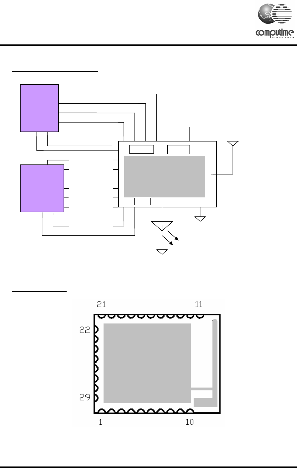
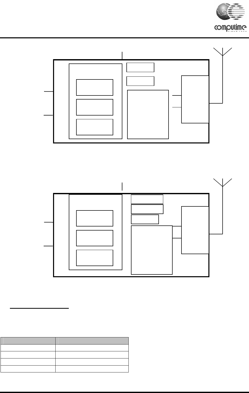
10. Block Diagram
CTL3576
CTL3577
PCB antenna
TO HOST
MCU
User
Application
ZigbeeTM
Network
IEEE 802.15.4
MAC
IEEE 802.15.4
RF Transceiver
2.7 – 3.6V
FEM
32 Bit ARM Processor 8Mb flash
24MHz
PCB antenna
TO HOST
MCU
User
Application
ZigbeeTM
Network
IEEE 802.15.4
MAC
IEEE 802.15.4
RF Transceiver
2.7 – 3.6V
FEM
32 Bit ARM Processor 24MHz
ZigBee- Ready RF Transceiver Module CTL3576/7/8/9
Copyright © 2011 Computime Limited. All rights reserved. Rev. 1
CTL3578
CTL3579
Figure 3: Block Diagram
11. RF Frequency Detail
The following table shows the RF channels as defined by the IEEE 802.15.4 standard.
RF channel Frequency
11 2405MHz
12 2410MHz
13 2415MHz
14 2420MHz
PCB antenna
TO HOST
MCU
User
Application
ZigbeeTM
Network
IEEE 802.15.4
MAC
IEEE 802.15.4
RF Transceiver
2.7 – 3.6V
FEM
32 Bit ARM Processor 32.768kHz
24MHz
PCB antenna
TO HOST
MCU
User
Application
ZigbeeTM
Network
IEEE 802.15.4
MAC
IEEE 802.15.4
RF Transceiver
2.7 – 3.6V
FEM
32 Bit ARM Processor 8Mb flash
32.768kHz
24MHz
ZigBee- Ready RF Transceiver Module CTL3576/7/8/9
Copyright © 2011 Computime Limited. All rights reserved. Rev. 1
15 2425MHz
16 2430MHz
17 2435MHz
18 2440MHz
19 2445MHz
20 2450MHz
21 2455MHz
22 2460MHz
23 2465MHz
24 2470MHz
25 2475MHz
26 2480MHz
Note: the output power of EM357 should be configured lower than -15dBm for 2480M channel
to Comply FCC requirement.
The use of RF frequencies and maximum allowed RF power should according to different national
regulations. The CTL3576 is complying with the applicable regulations for the world wide 2.4GHz
ISM band.
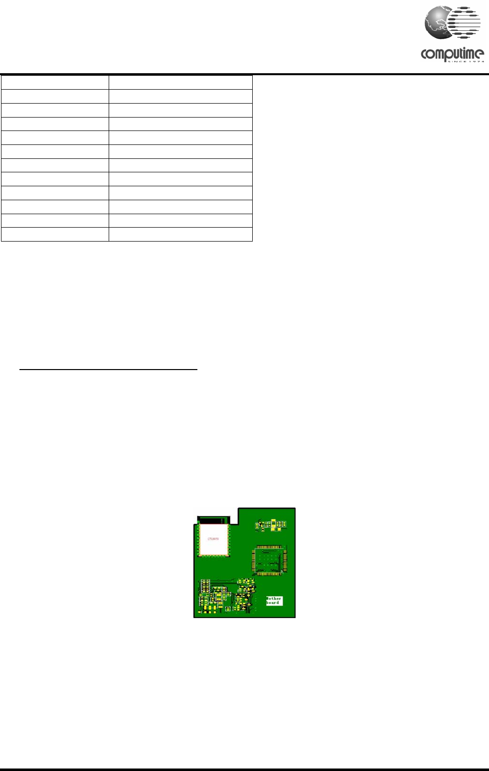
12.
PCB Layout Recommendations
Please reference Mechanical Dimensions shown in next section for PCB layout.
The area underneath the module should be covered with solder mask in order to prevent short
circuit on the test pads on the back side of the module. A solid ground plane under the module is
preferred.
As the module integrated with onboard PCB trace antenna, the mounting position of the module will
have great impact on the RF performance. There should not be any trace, ground plane or metal
part underneath or nearby the area of the onboard PCB trace antenna. The figure below shows an
example how the module positioned on the mother PCB.
Figure 4: A recommended placement of the module on a main PCB
ZigBee- Ready RF Transceiver Module CTL3576/7/8/9
Copyright © 2011 Computime Limited. All rights reserved. Rev. 1
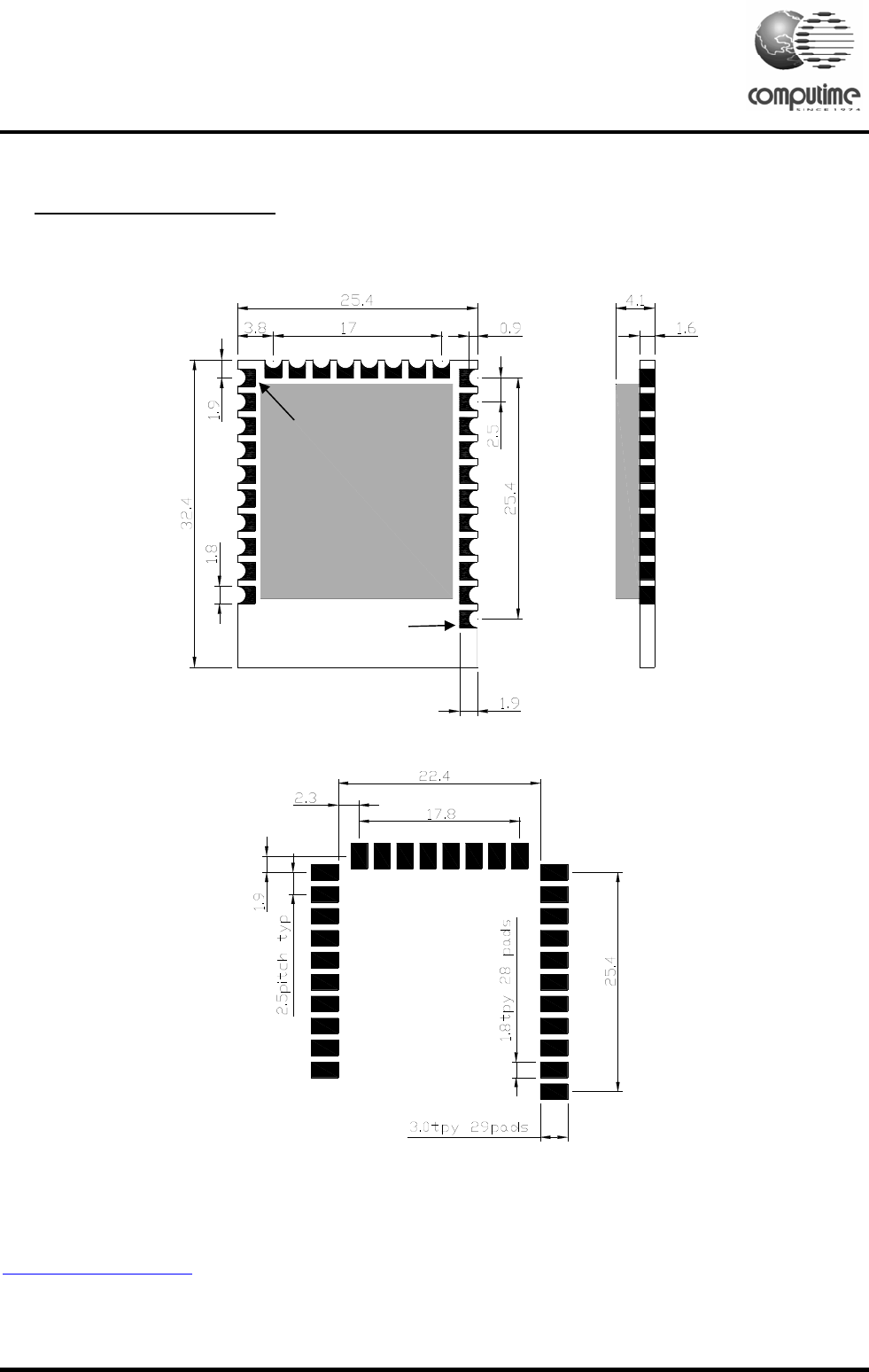
13. Mechanical Dimensions
Figure 5: Mechanical Dimensions of CTL3576
.8
For further details on the SoC transceiver (Ember EM357), please consult the data sheet at
http://www.ember.com
Pin 1
Pin 11

ZigBee- Ready RF Transceiver Module CTL3576/7/8/9
Copyright © 2011 Computime Limited. All rights reserved. Rev. 1
14. Modules Differentia
Computime Model No. P.A. 32kHz Crystal 8Mbit Flash Memory
CTL3576 Y N N
CTL3577 Y N Y
CTL3578 Y Y N
CTL3579 Y Y Y

FCC STATEMENT:
1. This device complies with part 15 of the FCC Rules. Operation is subject to the following
two conditions:
(1) This device may not cause harmful interference, and
(2) this device must accept any interference received, including interference that may cause
undesired operation.
2. Changes or modifications not expressly approved by the party responsible for compliance
could void the user's authority to operate the equipment.
NOTE: This equipment has been tested and found to comply with the limits for a Class B
digital device, pursuant to Part 15 of the FCC Rules. These limits are designed to provide
reasonable protection against harmful interference in a residential installation. This
equipment generates, uses and can radiate radio frequency energy and, if not installed and
used in accordance with the instructions, may cause harmful interference to radio
communications. However, there is no guarantee that interference will not occur in a
particular installation. If this equipment does cause harmful interference to radio or television
reception, which can be determined by turning the equipment off and on, the user is
encouraged to try to correct the interference by one or more of the following measures:
-- Reorient or relocate the receiving antenna.
-- Increase the separation between the equipment and receiver.
-- Connect the equipment into an outlet on a circuit different from that to which the receiver is
connected.
-- Consult the dealer or an experienced radio/TV technician for help.
FCC Radiation Exposure Statement
The modular can be installed or integrated in mobile or fix devices only. This modular cannot
be installed in any portable device, for example, USB dongle like transmitters is forbidden.
This modular complies with FCC RF radiation exposure limits set forth for an uncontrolled
environment. This transmitter must not be co-located or operating in conjunction with any
other antenna or transmitter. This modular must be installed and operated with a minimum
distance of 20 cm between the radiator and user body.
If the FCC identification number is not visible when the module is installed inside another
device, then the outside of the device into which the module is installed must also display a
label referring to the enclosed module. This exterior label can use wording such as the
following: “Contains Transmitter Module FCC ID: DI2-CTL3579A
when the module is installed inside another device, the user manual of this device must
contain below warning statements;
1. This device complies with Part 15 of the FCC Rules. Operation is subject to the following
two conditions:
(1) This device may not cause harmful interference.
(2) This device must accept any interference received, including interference that may cause
undesired operation.
2. Changes or modifications not expressly approved by the party responsible for compliance
could void the user's authority to operate the equipment.
The devices must be installed and used in strict accordance with the manufacturer's
instructions as described in the user documentation that comes with the product.
Le présent appareil est conforme aux CNR d'Industrie Canada applicables aux
appareils radio exempts de licence. L'exploitation est autorisée aux deux conditions
suivantes : (1) l'appareil ne doit pas produire de brouillage, et (2) l'utilisateur de
l'appareil doit accepter tout brouillage radioélectrique subi, même si le brouillage est
susceptible d'en compromettre le fonctionnement.
IC RF warning statement
This equipment complies with IC radiation exposure limits set forth for an uncontrolled environment.
This equipment should be installed and operated with minimum distance 20cm between the radiator &
your body.
If the IC identification number is not visible when the module is installed inside another
device, then the outside of the device into which the module is installed must also display a
label referring to the enclosed module. This exterior label can use wording such as the
following: “Contains Transmitter Module IC: 1700D-CTL3579A
IC: 1700D-CTL3579A
Model No.:CTL3579, CTL3576, CTL3577, CTL3578
Antenna type:intergal (SMT)
Antenna gain:-0.32dBi
Antenna impedance: 50ohm
Under Industry Canada regulations, this radio transmitter may only operate using an antenna of a
type and maximum (or lesser) gain approved for the transmitter by Industry Canada. To reduce
potential radio interference to other users, the antenna type and its gain should be so chosen that
the equivalent isotropically radiated power (e.i.r.p.) is not more than that necessary for successful
communication.
Canada information:
This device complies with Industry Canada licence-exempt RSS standard(s). Operation is subject to the
following two conditions:
(1) this device may not cause interference, and (2) this device must accept any interference, including
interference that may cause undesired operation of the device.

ZigBee- Ready RF Transceiver Module CTL3576/7/8/9
Copyright © 2011 Computime Limited. All rights reserved. Rev. 1
Contact information
COMPUTIME CORPORATE HQ
17/F, Great Eagle Centre,
23 Harbour Road, Wanchai,
Tel: +852.2260.0300
Fax: +852.2790.3996
e-mail: hq@computime.com
COMPUTIME NORTH AMERICA HQ,
4700 Duke Dr.
Suite 200
Mason OH 45040
USA
Tel: +1(513).398.2579
Fax: +1(513).754.8955
e-mail: na@computime.com
CINCINNATI WIRELESS SOLUTIONS LTD
4700 Duke Dr.
Suite 200
Mason OH 45040
USA
Tel: +1(513).754.8935
Fax: +1(513).754.8955
e-mail: ctws@computime.com
COMPUTIME JAPAN
3-18-9 Roppongi Minatoku,
Tokyo 106-0032,
Japan
Tel: (03).3583.8411
Fax: (03).3583.3799
e-mail: cj@computime.com
About Computime
Founded in 1974, Computime is a global technology, brand and manufacturing company
providing innovative automation and control solutions to customers in commercial, industrial
and consumer markets.
The Company provides technologies and products that save energy and make people's
lives more productive and comfortable.