Conexant Systems 36342U Spread Spectrum Transmitter User Manual AN9949
Conexant Systems Inc. Spread Spectrum Transmitter AN9949
UserManual.wiki
>
Conexant Systems
>
36342U User Manual
>
Manual
Contents
1.
Manual
2.
Addendum to manual
Manual
Navigation menu
Upload a User Manual
Namespaces
Wiki Guide
HTML
PDF
Info
Views
User Manual
Discussion / Help
Navigation
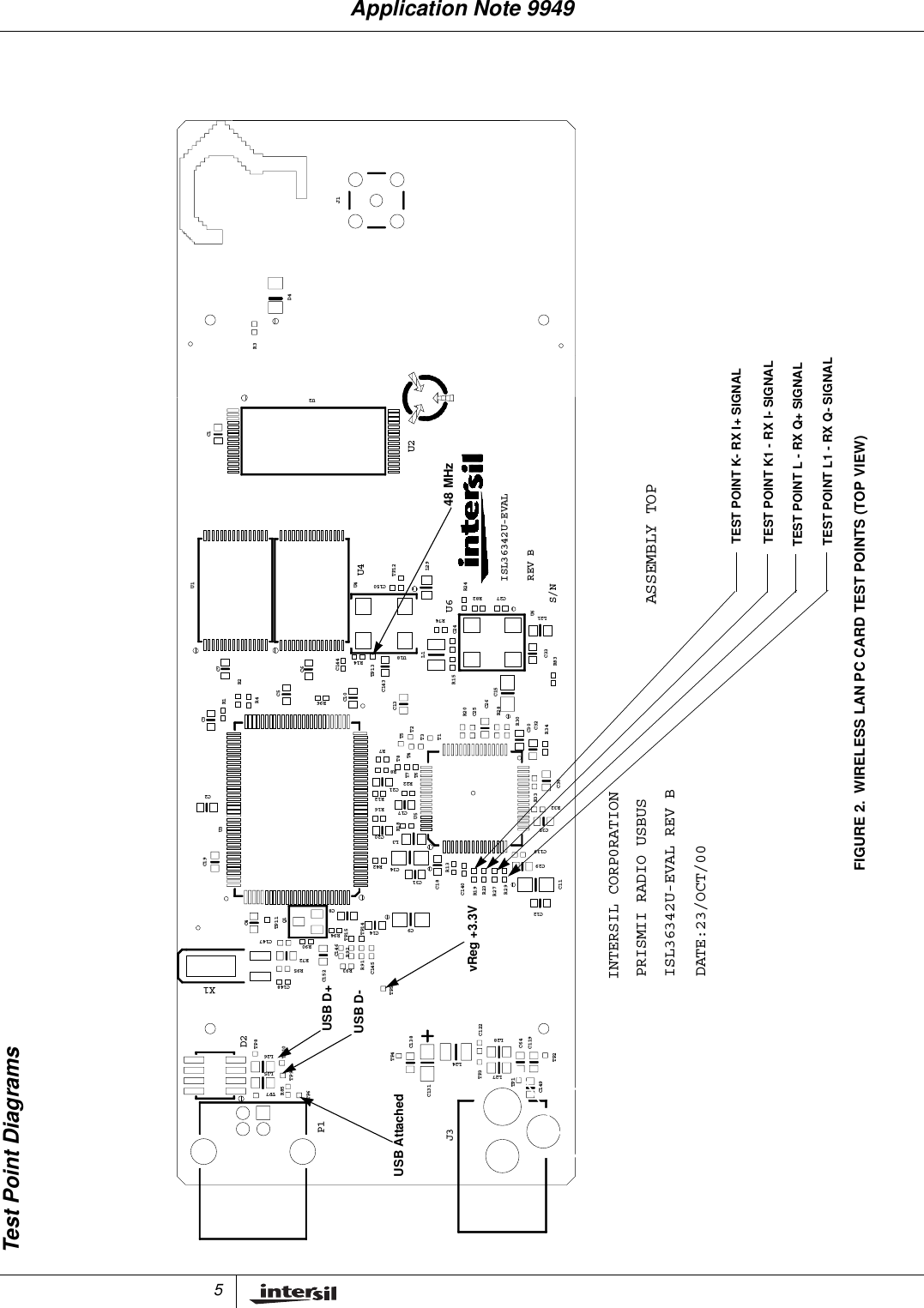
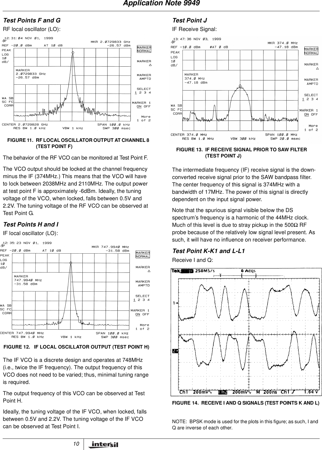
![11The receive In-phase and Quadrature (I and Q) signals arethe demodulated lowpass-filtered data that are coupled tothe HFA3861. The output levels of these two signals areapproximately 500mVP-P. As these are balanced signals,data is taken using a Tektronix P6247 Differential Probe.• Test point K for RXI+ signal is at the 0Ωjumper, R19.• Test point K1 for RXI- signal is at the 0Ωjumper, R23• Test point L for RXQ+ signal is at the 0Ωjumper, R27• Test point L1 for RXQ- signal is at the 0Ωjumper, R29.Operational CharacteristicsSee the iSL36342U-EVAL data sheet, Intersil File NumberFN8018, for more detailed specifications.ReferencesFor Intersil documents available on the internet, see web sitewww.intersil.com[1] iSL36342U-EVAL Data Sheet, Intersil Corporation.[2] AN9850 Application Note, Intersil Corporation,“Complementary Code Keying Made Simple”.NoticesElectronic Emission NoticesThis device complies with Part 15 of the FCC rules.Operation is subject to the following two conditions:1. This device may not cause harmful interference.2. This device must accept any interference received,including interference that may cause undesiredoperation.FCC Radio Frequency Interference StatementThe wireless LAN PC card is subject to the rules of theFederal Communications Commission (FCC). This card isconsidered an intentional radiator as per the FCC guidelines.NOTE: This equipment has been tested and found to comply withthe limits for a Class B digital device, pursuant to Part 15 of the FCCrules. These limits are designed to provide reasonable protectionagainst harmful interference in a residential installation. Thisequipment generates, uses and can radiate radio frequency energyand, if not installed and used in accordance with the instructionmanual, may cause harmful interference to radio communications.However, there is no guarantee that interference will not occur in aparticular installation. If this equipment does cause harmfulAbsolute Maximum RatingsSupplyVoltage..........................-0.3Vto7.0V(Max)StorageTemperature(Note1).................. -20oCto65oCOperating ConditionsTemperatureRange........................ 0oC≤ TA≤55oCSupplyVoltageRange.......................... 4.20Vto7VCaution: These are the absolute maximum ratings for the PC Card product.Exceeding these limits could cause permanent damage to the card.NOTE:1. All temperature references refer to ambient conditions.TABLE 4. GENERAL SPECIFICATIONSSPECIFICATION VALUETargeted Standard IEEE 802.11Data Rate 1Mbps DBPSK2Mbps DQPSK5.5Mbps CCK11Mbps CCKRange (11Mbps Data Rate) 120ft (37M) Indoor (Typ)400ft (122M) Outdoor (Typ)Center Frequency Range 2412MHz - 2484MHzStep Size 1MHzIF Frequency 374MHz1.875"FIGURE 15. EDGE VIEW, USB CARDIF Bandwidth 17MHzRX/TX Switching Speed 2µs(Typ)Average Current withoutPower Save2% Transmit, 98% Receive187mA (Typ)Average Current with PowerSave2% TX, 8% RX, 90% Standby43mA (Typ)Current in Continuous TXmode300mA (Typ)Current in Continuous RXMode185mA (Typ)Standby Current 25mA (Typ)Mechanical PC Card, with Antenna ExtensionOutput Power +11.5dBm (Typ)Transmit Spectral Mask -30dBc at First Side LobesAntenna Interface SMA, 50Ω (for Testing Only)Dual Diversity Printed AntennaTABLE 4. GENERAL SPECIFICATIONSSPECIFICATION VALUEApplication Note 9949](https://usermanual.wiki/Conexant-Systems/36342U.Manual/User-Guide-162113-Page-11.png)