Continental Automotive Systems 5WY8230 Remote Keyless Entry Receiver User Manual Manual Function 5WY8222
Continental Automotive Systems Corporation Remote Keyless Entry Receiver Manual Function 5WY8222
UserManual.wiki
>
Continental Automotive Systems
>
5WY8230 User Manual
User Manual
Navigation menu
Upload a User Manual
Namespaces
Wiki Guide
HTML
PDF
Info
Views
User Manual
Discussion / Help
Navigation
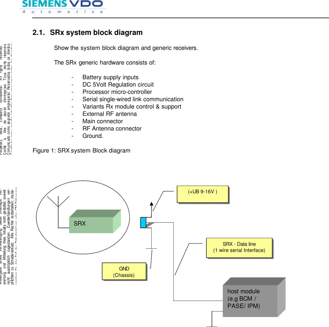
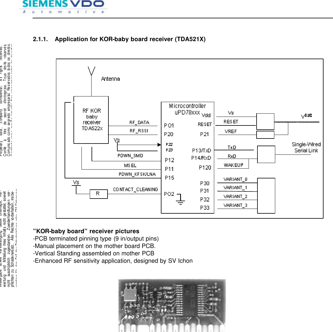
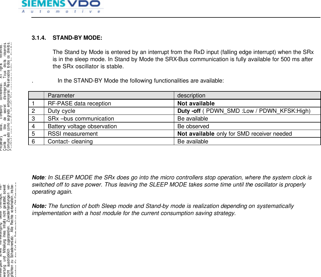
![Propietary data, company confidential. All rights reserved.Confié à titre de secret d'entreprise. Tous droits réservé s.Comunicado como segredo empresarial. Reservados todos os direitos.Confidado como secreto industial. Nos reservamos todos los derechos. Weitergabe sowie Vervielfältigung dieser Unterlage, Ver-wertung und Mitteilung ihres Inhalts nicht gestattet, soweitnicht ausdrücklich zugestanden. Zuwiderhandlungen ver-pflichten zu Schadenersatz. Alle Rechte vorbehalten, insbe-sondere für den Fall der Patenterteilung oder GM-Eintragung. Table of Contents page 1. GENERAL.......................................................................................................................................................................................3 1.1. DEFINITIONS AND ABBREVIATIONS.................................................................................................................................. 4 2. SYSTEM DESCRIPTION............................................................................................................................................................5 2.1. SRX SYSTEM BLOCK DIAGRAM........................................................................................................................................... 6 2.1.1. Application for KOR-baby board receiver (TDA521X) .......................................................................................7 2.2. SRX MODULE PIN –OUT CONFIGURATION ...................................................................................................................... 8 2.2.1. Main connector X1 .....................................................................................................................................................8 2.2.2. RF antenna connector X2..........................................................................................................................................8 3. FUNCTION ELECTRICAL DESCRIPTION ............................................................................................................................9 3.1. SRX OPERATION MODES.................................................................................................................................................... 9 3.1.1. RKE MODE...................................................................................................................................................................9 3.1.2. PASE MODE.................................................................................................................................................................9 3.1.3. SLEEP MODE ..............................................................................................................................................................9 3.1.4. STAND-BY MODE:....................................................................................................................................................10 3.2. DUTY CONTROL FOR PDWN............................................................................................................................................ 11 3.3. MODULATION SELECTION FOR MSEL............................................................................................................................ 11 3.4. RSSI (RECEIVED SIGNAL STRENGTH INDICATOR) FOR RANGE REDUCTION............................................................. 11 3.5. DEMODULATED DATA OUT FOR RF_DATA................................................................................................................. 12 3.5.1. Data Output Electrical Characteristics: ..............................................................................................................12 3.6. SRX DATA LINE (SERIAL INTERFACE) SRX_COM FOR RXD / TXD / WAKEUP.................................................... 12 3.7. BATTERY VOLTAGE REFERENCE OBSERVATION .......................................................................................................... 12 4. SRX SYSTEM ELECTRICAL SPECIFICATION..................................................................................................................12 4.1. OPERATING TEMPERATURE RANGE OF SRX................................................................................................................. 12 4.2. OPERATING VOLTAGE RANGE OF SRX........................................................................................................................... 12 4.3. QUIESCENT CURRENT [I S]................................................................................................................................................ 13 5. MICRO-PROCESSOR DESCRIPTION.................................................................................................................................13 6. RF TECHNICAL DESCRIPTION............................................................................................................................................14 6.1. RF INPUT SENSITIVITY...................................................................................................................................................... 14 6.1.1. RF input sensitivity...................................................................................................................................................14 6.1.2. RF data output demodulation polarity.................................................................................................................14 7. SYSTEM COMPATIBILITY WITH TX FREQUENCY TOLERANCE..............................................................................14 7.1.1. 3 dB sensitivity degradation...................................................................................................................................14](https://usermanual.wiki/Continental-Automotive-Systems/5WY8230/User-Guide-538988-Page-2.png)
![Propietary data, company confidential. All rights reserved.Confié à titre de secret d'entreprise. Tous droits réservé s.Comunicado como segredo empresarial. Reservados todos os direitos.Confidado como secreto industial. Nos reservamos todos los derechos. Weitergabe sowie Vervielfältigung dieser Unterlage, Ver-wertung und Mitteilung ihres Inhalts nicht gestattet, soweitnicht ausdrücklich zugestanden. Zuwiderhandlungen ver-pflichten zu Schadenersatz. Alle Rechte vorbehalten, insbe-sondere für den Fall der Patenterteilung oder GM-Eintragung. 3.5. Demodulated data out for RF_DATA After process of demodulation by corresponding receiver, which data telegram transfer to the input port as RF_DATA. 3.5.1. Data Output Electrical Characteristics: For KOR-baby board receiver, Vs=5V, 1% Parameter Min Typ Max Unit Remark 1 High output voltage Vs-1.3 Vs-0.7 V 2 Low output voltage 0 0.2 V 3.6. SRX Data line (serial Interface) SRX_COM for RxD / TxD / WAKEUP The SRX have two system configurations for support an RKE –only system (BCM) and PASE PIC with bi-directional communication line. The communication speed is 2.4k baud for BCM or 9.6k baud for PASE PIC, After a valid SHARK RKE telegram was successfully received the SRx must transmit the RKE data to the host module via serial link. Special care has to be taken for the following cases. And for the data serial line full-up condition is a corresponded host module has to be full-upped to battery voltage with a resister values 1.2K Ohm 3.7. Battery voltage reference observation To observe the battery voltage with the processor input port as VREF At the V_BAT input line. Parameter min Typ max Unit Remark 1 Over voltage threshold range 16 16.8 V 2 Under voltage threshold range 8.5 9 V 4. SRx System Electrical Specification 4.1. Operating Temperature Range of SRx Parameter Min Typ Max Unit Remark 1 Operating temperature range -40 +85 °C 2 Storage temperature range -40 +85 °C 4.2. Operating Voltage Range of SRx Parameter Min Typ Max Unit Remark 1 Operating voltage range [U b] 9 16 V VBAT 2 Reverse voltage protection -13 V For 5 minutes](https://usermanual.wiki/Continental-Automotive-Systems/5WY8230/User-Guide-538988-Page-12.png)
![Propietary data, company confidential. All rights reserved.Confié à titre de secret d'entreprise. Tous droits réservé s.Comunicado como segredo empresarial. Reservados todos os direitos.Confidado como secreto industial. Nos reservamos todos los derechos. Weitergabe sowie Vervielfältigung dieser Unterlage, Ver-wertung und Mitteilung ihres Inhalts nicht gestattet, soweitnicht ausdrücklich zugestanden. Zuwiderhandlungen ver-pflichten zu Schadenersatz. Alle Rechte vorbehalten, insbe-sondere für den Fall der Patenterteilung oder GM-Eintragung. The system has to operate at a DC voltage of U b=9V to 16V. The communication over the data line is limited between 9V to 16V. Out of 9V-16V range, the system must not operate, but no malfunction is allowed. The normal operating voltage is U b=12.8V ±0.2 during the IGN off and the operation voltage is U b=13.8V ±0.2 V duration IGN on. 4.3. Quiescent Current [I s] If the system is at RKE –stand by condition ( no communication action active) the worst case quiescent current must not be higher than Is over the whole working range [U b] and under worst case surrounding characteristics normally present in plants, different climate and temperature zones where the vehicle could be used by the customer. The typical quiescent current must not be higher than [I typ ] at 12.8V and at room temperature (RT=25°C) Parameter description 1 I typ @12.8V /RT < 3.5 mA Note: For typical quiescent current measure with the average values during the SRx on duty cycle running (vehicles under parking mode completely) The quiescent current in receiver off mode (all SRx functions is stopped) Parameter description 1 I typ @12.8V /RT (without LNA) < 0.5 mA 2 I typ @12.8V /RT (with LNA) < 0.5 mA Under worst case conditions (16V, 85°C) the current Iworst case may increase by 20% of Ityp . Note: For the current measuring use only a correct tool with a maximum measurement range to 100 mA 5. Micro-processor description The processor of the SRx was selected as 8-bit Single-chip NEC’s Micro-controller with 78KO series µPD780XXX. Target processor is µPD780102 with masked. But for the development support, the SRx will be used with flash memory processor µPD78F0103 in order to offer facilities to SW development. The Micro controller µPD780102 has the following memories: - Internal ROM 16K bytes - High speeds RAM 768 bytes - Memory space 64K bytes - CPU system Clock 4.953 MHz with ceramic resonator - Support the Flash memory programming](https://usermanual.wiki/Continental-Automotive-Systems/5WY8230/User-Guide-538988-Page-13.png)
![Propietary data, company confidential. All rights reserved.Confié à titre de secret d'entreprise. Tous droits réservé s.Comunicado como segredo empresarial. Reservados todos os direitos.Confidado como secreto industial. Nos reservamos todos los derechos. Weitergabe sowie Vervielfältigung dieser Unterlage, Ver-wertung und Mitteilung ihres Inhalts nicht gestattet, soweitnicht ausdrücklich zugestanden. Zuwiderhandlungen ver-pflichten zu Schadenersatz. Alle Rechte vorbehalten, insbe-sondere für den Fall der Patenterteilung oder GM-Eintragung. 6. RF technical description 6.1. RF input sensitivity There are two of definitions for the RF input sensitivity, first of case is integrated with LNA circuit for high gain antenna performance, second of case is no integrated with LNA circuit as by passed LNA routing to the receiver RF input. 6.1.1. RF input sensitivity For KOR-baby board FSK receiver @ conducted Typical sensitivity [dBm] Min. sensitivity @RT [dBm] Frequency Variant Data Rate [kbit/s] FSK ±35kHz dev. FSK ±35kHz dev. 315.00 MHz 5WY 8230 (1k) 1 - 111 -108 Input sensitivity at center frequency, BER 10-2 (Vcc = 5V) 6.1.2. RF data output demodulation polarity ASK RF Signal RF On RF Off RX DATA output HIGH LOW FSK RF Signal RF on RF Off RX DATA output HIGH HIGH random (from noise FM compared) 7. System compatibility with TX Frequency Tolerance System compatibility with TX Frequency Tolerance is restricted, in order to stay (for the worst-case scenario) within 3 dB sensitivity degradation. 7.1.1. 3 dB sensitivity degradation Max tolerance of transmitter frequency from nominal carrier frequency ("min. sensitivity 3 dB bandwidth"): The transmitter should be considered enough as below For KOR-baby board receiver T = -40° to +85°C Max. allowed deviation of TX frequency from nominal frequency Frequency band FSK ±35kHz deviation -70 kHz +44 kHz 315 MHz -222 ppm +139 ppm](https://usermanual.wiki/Continental-Automotive-Systems/5WY8230/User-Guide-538988-Page-14.png)