Continental Automotive Systems 5WY8230 Remote Keyless Entry Receiver User Manual Manual Function 5WY8222
Continental Automotive Systems Corporation Remote Keyless Entry Receiver Manual Function 5WY8222
User Manual
P
r
o
p
r
i
e
t
a
r
y
d
a
t
a
,
c
o
m
p
a
n
y
c
o
n
f
i
d
e
n
t
i
a
l
.
A
l
l
r
i
g
h
t
s
r
e
s
e
r
v
e
d
.
Confié à titre de secret d'entreprise. Tous droits réservés.
Comunicado como segredo empresarial. Reservados todos os direitos.
C
o
n
f
i
d
a
d
o
c
o
m
o
s
e
c
r
e
t
o
i
n
d
u
s
t
r
i
a
l
.
N
o
s
r
e
s
e
r
v
a
m
o
s
t
o
d
o
s
l
o
s
d
e
r
e
c
h
o
s
.
W
e
i
t
e
r
g
a
b
e
s
o
w
i
e
V
e
r
v
i
e
l
f
ä
l
t
i
g
u
n
g
d
i
e
s
e
r
U
n
t
e
r
l
a
g
e
,
V
e
r
-
wertung und Mitteilung ihres Inhalts nicht gestattet, soweit
nicht ausdrücklich zugestanden. Zuwiderhandlungen ver-
pflichten zu Schadenersatz. Alle Rechte vorbehalten, insbe-
s
o
n
d
e
r
e
f
ü
r
d
e
n
F
a
l
l
d
e
r
P
a
t
e
n
t
e
r
t
e
i
l
u
n
g
o
d
e
r
G
M
-
E
i
n
t
r
a
g
u
n
g
.
Functional Description
of
Siemens Korea RF SRX module
Type: 5WY8230(for 315MHz)

P
r
o
p
i
e
t
a
r
y
d
a
t
a
,
c
o
m
p
a
n
y
c
o
n
f
i
d
e
n
t
i
a
l
.
A
l
l
r
i
g
h
t
s
r
e
s
e
r
v
e
d
.
Confié à titre de secret d'entreprise. Tous droits réservé s.
Comunicado como segredo empresarial. Reservados todos os direitos.
C
o
n
f
i
d
a
d
o
c
o
m
o
s
e
c
r
e
t
o
i
n
d
u
s
t
i
a
l
.
N
o
s
r
e
s
e
r
v
a
m
o
s
t
o
d
o
s
l
o
s
d
e
r
e
c
h
o
s
.
W
e
i
t
e
r
g
a
b
e
s
o
w
i
e
V
e
r
v
i
e
l
f
ä
l
t
i
g
u
n
g
d
i
e
s
e
r
U
n
t
e
r
l
a
g
e
,
V
e
r
-
wertung und Mitteilung ihres Inhalts nicht gestattet, soweit
nicht ausdrücklich zugestanden. Zuwiderhandlungen ver-
pflichten zu Schadenersatz. Alle Rechte vorbehalten, insbe-
s
o
n
d
e
r
e
f
ü
r
d
e
n
F
a
l
l
d
e
r
P
a
t
e
n
t
e
r
t
e
i
l
u
n
g
o
d
e
r
G
M
-
E
i
n
t
r
a
g
u
n
g
.
Table of Contents page
1. GENERAL.......................................................................................................................................................................................3
1.1. DEFINITIONS AND ABBREVIATIONS.................................................................................................................................. 4
2. SYSTEM DESCRIPTION............................................................................................................................................................5
2.1. SRX SYSTEM BLOCK DIAGRAM........................................................................................................................................... 6
2.1.1. Application for KOR-baby board receiver (TDA521X) .......................................................................................7
2.2. SRX MODULE PIN –OUT CONFIGURATION ...................................................................................................................... 8
2.2.1. Main connector X1 .....................................................................................................................................................8
2.2.2. RF antenna connector X2..........................................................................................................................................8
3. FUNCTION ELECTRICAL DESCRIPTION ............................................................................................................................9
3.1. SRX OPERATION MODES.................................................................................................................................................... 9
3.1.1. RKE MODE...................................................................................................................................................................9
3.1.2. PASE MODE.................................................................................................................................................................9
3.1.3. SLEEP MODE ..............................................................................................................................................................9
3.1.4. STAND-BY MODE:....................................................................................................................................................10
3.2. DUTY CONTROL FOR PDWN............................................................................................................................................ 11
3.3. MODULATION SELECTION FOR MSEL............................................................................................................................ 11
3.4. RSSI (RECEIVED SIGNAL STRENGTH INDICATOR) FOR RANGE REDUCTION............................................................. 11
3.5. DEMODULATED DATA OUT FOR RF_DATA................................................................................................................. 12
3.5.1. Data Output Electrical Characteristics: ..............................................................................................................12
3.6. SRX DATA LINE (SERIAL INTERFACE) SRX_COM FOR RXD / TXD / WAKEUP.................................................... 12
3.7. BATTERY VOLTAGE REFERENCE OBSERVATION .......................................................................................................... 12
4. SRX SYSTEM ELECTRICAL SPECIFICATION..................................................................................................................12
4.1. OPERATING TEMPERATURE RANGE OF SRX................................................................................................................. 12
4.2. OPERATING VOLTAGE RANGE OF SRX........................................................................................................................... 12
4.3. QUIESCENT CURRENT [I S]................................................................................................................................................ 13
5. MICRO-PROCESSOR DESCRIPTION.................................................................................................................................13
6. RF TECHNICAL DESCRIPTION............................................................................................................................................14
6.1. RF INPUT SENSITIVITY...................................................................................................................................................... 14
6.1.1. RF input sensitivity...................................................................................................................................................14
6.1.2. RF data output demodulation polarity.................................................................................................................14
7. SYSTEM COMPATIBILITY WITH TX FREQUENCY TOLERANCE..............................................................................14
7.1.1. 3 dB sensitivity degradation...................................................................................................................................14
P
r
o
p
i
e
t
a
r
y
d
a
t
a
,
c
o
m
p
a
n
y
c
o
n
f
i
d
e
n
t
i
a
l
.
A
l
l
r
i
g
h
t
s
r
e
s
e
r
v
e
d
.
Confié à titre de secret d'entreprise. Tous droits réservé s.
Comunicado como segredo empresarial. Reservados todos os direitos.
C
o
n
f
i
d
a
d
o
c
o
m
o
s
e
c
r
e
t
o
i
n
d
u
s
t
i
a
l
.
N
o
s
r
e
s
e
r
v
a
m
o
s
t
o
d
o
s
l
o
s
d
e
r
e
c
h
o
s
.
W
e
i
t
e
r
g
a
b
e
s
o
w
i
e
V
e
r
v
i
e
l
f
ä
l
t
i
g
u
n
g
d
i
e
s
e
r
U
n
t
e
r
l
a
g
e
,
V
e
r
-
wertung und Mitteilung ihres Inhalts nicht gestattet, soweit
nicht ausdrücklich zugestanden. Zuwiderhandlungen ver-
pflichten zu Schadenersatz. Alle Rechte vorbehalten, insbe-
s
o
n
d
e
r
e
f
ü
r
d
e
n
F
a
l
l
d
e
r
P
a
t
e
n
t
e
r
t
e
i
l
u
n
g
o
d
e
r
G
M
-
E
i
n
t
r
a
g
u
n
g
.
FCC Compliance statement
This equipment has been tested and found to comply with the limits for a Class B digital device, pursuant to
part 15 of the FCC Rules. These limits are designed to provide reasonable protection against harmful
interference in a residential installation.
This equipment generates, uses and can radiate radio frequency energy and, if not installed and used in
accordance with the instructions, may cause harmful interference to radio communications. However, there is
no guarantee that interference will not occur in a particular installation. If this equipment does cause harmful
interference to radio or television reception, which can be determined by turning the equipment off and on, the
user is encouraged to try to correct the interference by one or more of the following measures:
— Reorient or relocate the receiving antenna.
— Increase the separation between the equipment and receiver.
— Connect the equipment into an outlet on a circuit different from that to which the receiver is connected.
— Consult the dealer or an experienced radio/TV technician for help.
Caution: You are cautioned that any changes or modifications to the equipment
not expressly approved by the party responsible for compliance could void your
authority to operate the equipment.
This device complies with part 15 of the FCC Rules. Operation
is subject to the following two conditions:
(1) This device may not cause harmful interference, and
(2) This device must accept any interference received,
including interference that may cause undesired operation.

P
r
o
p
i
e
t
a
r
y
d
a
t
a
,
c
o
m
p
a
n
y
c
o
n
f
i
d
e
n
t
i
a
l
.
A
l
l
r
i
g
h
t
s
r
e
s
e
r
v
e
d
.
Confié à titre de secret d'entreprise. Tous droits réservé s.
Comunicado como segredo empresarial. Reservados todos os direitos.
C
o
n
f
i
d
a
d
o
c
o
m
o
s
e
c
r
e
t
o
i
n
d
u
s
t
i
a
l
.
N
o
s
r
e
s
e
r
v
a
m
o
s
t
o
d
o
s
l
o
s
d
e
r
e
c
h
o
s
.
W
e
i
t
e
r
g
a
b
e
s
o
w
i
e
V
e
r
v
i
e
l
f
ä
l
t
i
g
u
n
g
d
i
e
s
e
r
U
n
t
e
r
l
a
g
e
,
V
e
r
-
wertung und Mitteilung ihres Inhalts nicht gestattet, soweit
nicht ausdrücklich zugestanden. Zuwiderhandlungen ver-
pflichten zu Schadenersatz. Alle Rechte vorbehalten, insbe-
s
o
n
d
e
r
e
f
ü
r
d
e
n
F
a
l
l
d
e
r
P
a
t
e
n
t
e
r
t
e
i
l
u
n
g
o
d
e
r
G
M
-
E
i
n
t
r
a
g
u
n
g
.
1. GENERAL
This is describes the hardware RF engineering of the stand alone RF receiver (SRx) for the HYUNDAI TG
project, which has the general RF Hardware and RF electrical specification for the remote control radio
frequency reception
1.1. Definitions and abbreviations
SRx : Stand- alone receiver (RX)
RKE : Remote Keyless Entry
RF : Radio Frequency
BCM : Body Control Module
PASE : Passive Access Start & Entry
IPM : In-Panel Module
PIC : Personal Identification Card
PDWN : Power Down
TG, BH ; Name of Hyundai motor vehicle platform
FSK ; Frequency Shift -Keying
ASK : Amplitude Shift- Keying
LNA : Low Noise Amplifier
Tx : Transmitter
Rx : Receiver
MSEL : Modulation Selection
RISS : Received Signal Strength Indicator
RxD : Receiving Data
TxD : Transmit Data
VREF : Voltage Reference
TP : Test Point
EOL : End of Line
VBAT : Voltage Battery
TTGD : Time To Good Data
VSWR : Voltage Standing Wave Ratio
ECU : Electronic Control Unit
ICT : In- Circuit Test
OST : Oscillation Stabilization Time

P
r
o
p
i
e
t
a
r
y
d
a
t
a
,
c
o
m
p
a
n
y
c
o
n
f
i
d
e
n
t
i
a
l
.
A
l
l
r
i
g
h
t
s
r
e
s
e
r
v
e
d
.
Confié à titre de secret d'entreprise. Tous droits réservé s.
Comunicado como segredo empresarial. Reservados todos os direitos.
C
o
n
f
i
d
a
d
o
c
o
m
o
s
e
c
r
e
t
o
i
n
d
u
s
t
i
a
l
.
N
o
s
r
e
s
e
r
v
a
m
o
s
t
o
d
o
s
l
o
s
d
e
r
e
c
h
o
s
.
W
e
i
t
e
r
g
a
b
e
s
o
w
i
e
V
e
r
v
i
e
l
f
ä
l
t
i
g
u
n
g
d
i
e
s
e
r
U
n
t
e
r
l
a
g
e
,
V
e
r
-
wertung und Mitteilung ihres Inhalts nicht gestattet, soweit
nicht ausdrücklich zugestanden. Zuwiderhandlungen ver-
pflichten zu Schadenersatz. Alle Rechte vorbehalten, insbe-
s
o
n
d
e
r
e
f
ü
r
d
e
n
F
a
l
l
d
e
r
P
a
t
e
n
t
e
r
t
e
i
l
u
n
g
o
d
e
r
G
M
-
E
i
n
t
r
a
g
u
n
g
.
2. SYSTEM DESCRIPTION
This Standalone (SRx) receiver has to support the receipt of RF telegram from transmitted in free air way by
corresponding transmitter and to transmit them to a host module (e.g. the Body Control Module and PIC
module).
Ø KOR-baby board receiver 315, FSK -1K data rate based on Infineon TDA 521x , which module
optimized maximum for the enhanced RF working range with LNA and data filter characterization.
All receipts of RF telegram has to be transmitted to a host module with the serial linked communication line
which line of single-wired serial link must be available to communicate with bi-directional for a bit rate 2.4k
bauds for BCM for a bit rate 9.6k bauds for PIC.
This SRx provide a variant 4 resistors with pull- Ground down for reading of mounted code.
The processor of the SRx was selected as 8-bit Single-chip NEC’s Micro-controller with 78KO series
The main function of generic SRx is
Ø RF signal detection (in-band)
Ø Data signal demodulation.
Ø Manchester and Shark protocol detection
Ø Self-polling for the standby current consumption
Ø Wake up function for the host module
Ø 315MHz RF data reception
Ø Serial communication with the single –wired link com.
P
r
o
p
i
e
t
a
r
y
d
a
t
a
,
c
o
m
p
a
n
y
c
o
n
f
i
d
e
n
t
i
a
l
.
A
l
l
r
i
g
h
t
s
r
e
s
e
r
v
e
d
.
Confié à titre de secret d'entreprise. Tous droits réservé s.
Comunicado como segredo empresarial. Reservados todos os direitos.
C
o
n
f
i
d
a
d
o
c
o
m
o
s
e
c
r
e
t
o
i
n
d
u
s
t
i
a
l
.
N
o
s
r
e
s
e
r
v
a
m
o
s
t
o
d
o
s
l
o
s
d
e
r
e
c
h
o
s
.
W
e
i
t
e
r
g
a
b
e
s
o
w
i
e
V
e
r
v
i
e
l
f
ä
l
t
i
g
u
n
g
d
i
e
s
e
r
U
n
t
e
r
l
a
g
e
,
V
e
r
-
wertung und Mitteilung ihres Inhalts nicht gestattet, soweit
nicht ausdrücklich zugestanden. Zuwiderhandlungen ver-
pflichten zu Schadenersatz. Alle Rechte vorbehalten, insbe-
s
o
n
d
e
r
e
f
ü
r
d
e
n
F
a
l
l
d
e
r
P
a
t
e
n
t
e
r
t
e
i
l
u
n
g
o
d
e
r
G
M
-
E
i
n
t
r
a
g
u
n
g
.
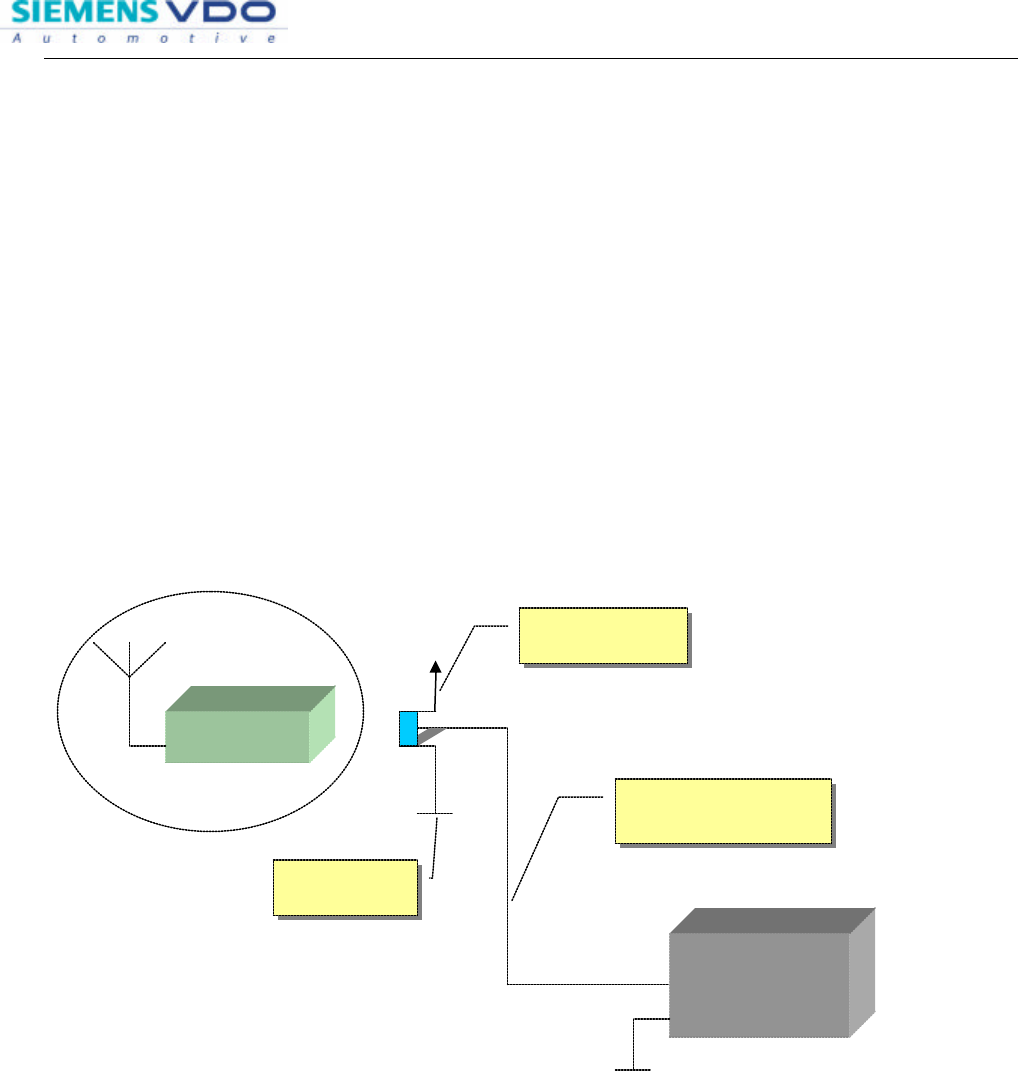
2.1. SRx system block diagram
Show the system block diagram and generic receivers.
The SRx generic hardware consists of:
- Battery supply inputs
- DC 5Volt Regulation circuit
- Processor micro-controller
- Serial single-wired link communication
- Variants Rx module control & support
- External RF antenna
- Main connector
- RF Antenna connector
- Ground.
Figure 1: SRX system Block diagram
SRX
host module
(e.g BCM /
PASE/ IPM)
SRX - Data line
(1 wire serial Interface)
(+UB 9-16V )
GND
(Chassis)
P
r
o
p
i
e
t
a
r
y
d
a
t
a
,
c
o
m
p
a
n
y
c
o
n
f
i
d
e
n
t
i
a
l
.
A
l
l
r
i
g
h
t
s
r
e
s
e
r
v
e
d
.
Confié à titre de secret d'entreprise. Tous droits réservé s.
Comunicado como segredo empresarial. Reservados todos os direitos.
C
o
n
f
i
d
a
d
o
c
o
m
o
s
e
c
r
e
t
o
i
n
d
u
s
t
i
a
l
.
N
o
s
r
e
s
e
r
v
a
m
o
s
t
o
d
o
s
l
o
s
d
e
r
e
c
h
o
s
.
W
e
i
t
e
r
g
a
b
e
s
o
w
i
e
V
e
r
v
i
e
l
f
ä
l
t
i
g
u
n
g
d
i
e
s
e
r
U
n
t
e
r
l
a
g
e
,
V
e
r
-
wertung und Mitteilung ihres Inhalts nicht gestattet, soweit
nicht ausdrücklich zugestanden. Zuwiderhandlungen ver-
pflichten zu Schadenersatz. Alle Rechte vorbehalten, insbe-
s
o
n
d
e
r
e
f
ü
r
d
e
n
F
a
l
l
d
e
r
P
a
t
e
n
t
e
r
t
e
i
l
u
n
g
o
d
e
r
G
M
-
E
i
n
t
r
a
g
u
n
g
.
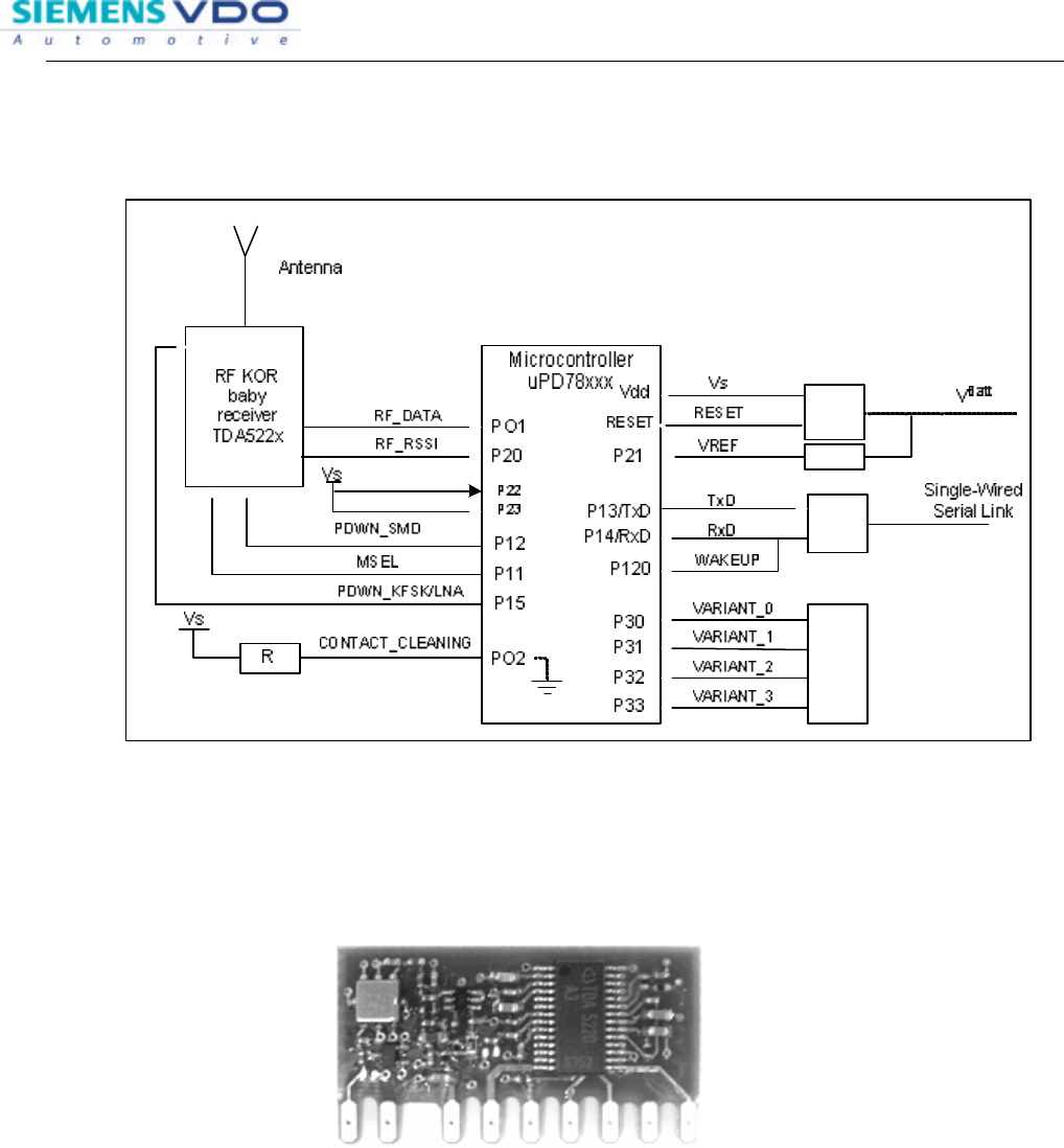
2.1.1. Application for KOR-baby board receiver (TDA521X)
”KOR-baby board” receiver pictures
-PCB terminated pinning type (9 in/output pins)
-Manual placement on the mother board PCB.
-Vertical Standing assembled on mother PCB
-Enhanced RF sensitivity application, designed by SV Ichon
P
r
o
p
i
e
t
a
r
y
d
a
t
a
,
c
o
m
p
a
n
y
c
o
n
f
i
d
e
n
t
i
a
l
.
A
l
l
r
i
g
h
t
s
r
e
s
e
r
v
e
d
.
Confié à titre de secret d'entreprise. Tous droits réservé s.
Comunicado como segredo empresarial. Reservados todos os direitos.
C
o
n
f
i
d
a
d
o
c
o
m
o
s
e
c
r
e
t
o
i
n
d
u
s
t
i
a
l
.
N
o
s
r
e
s
e
r
v
a
m
o
s
t
o
d
o
s
l
o
s
d
e
r
e
c
h
o
s
.
W
e
i
t
e
r
g
a
b
e
s
o
w
i
e
V
e
r
v
i
e
l
f
ä
l
t
i
g
u
n
g
d
i
e
s
e
r
U
n
t
e
r
l
a
g
e
,
V
e
r
-
wertung und Mitteilung ihres Inhalts nicht gestattet, soweit
nicht ausdrücklich zugestanden. Zuwiderhandlungen ver-
pflichten zu Schadenersatz. Alle Rechte vorbehalten, insbe-
s
o
n
d
e
r
e
f
ü
r
d
e
n
F
a
l
l
d
e
r
P
a
t
e
n
t
e
r
t
e
i
l
u
n
g
o
d
e
r
G
M
-
E
i
n
t
r
a
g
u
n
g
.
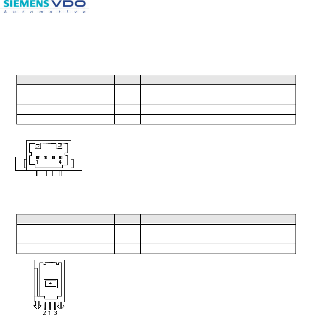
2.2. SRx module PIN –out configuration
To guarantee the full functionality of the RF system all lines listed below are mandatory.
2.2.1. Main connector X1
Digital / physical inputs Pin NO
Task description
SRX_COM X1-1 SRX Data line (serial Interface )
N.A X1-2 N.A reserved
V_BAT X1-3 Battery power supply input (9 V ~16V)
GND X1-4 SRX ground
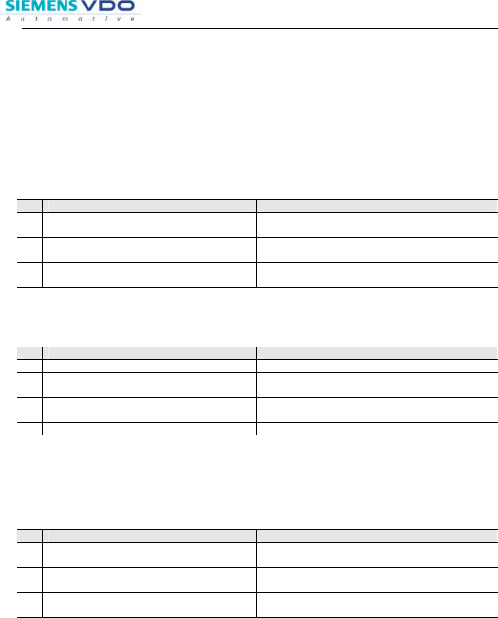
2.2.2. RF antenna connector X2
Digital / physical inputs PIN Task description
RF ANT-IN X2-1 RF antenna signal input
GND X2-2 Ground1
GND X2-3 Ground2
P
r
o
p
i
e
t
a
r
y
d
a
t
a
,
c
o
m
p
a
n
y
c
o
n
f
i
d
e
n
t
i
a
l
.
A
l
l
r
i
g
h
t
s
r
e
s
e
r
v
e
d
.
Confié à titre de secret d'entreprise. Tous droits réservé s.
Comunicado como segredo empresarial. Reservados todos os direitos.
C
o
n
f
i
d
a
d
o
c
o
m
o
s
e
c
r
e
t
o
i
n
d
u
s
t
i
a
l
.
N
o
s
r
e
s
e
r
v
a
m
o
s
t
o
d
o
s
l
o
s
d
e
r
e
c
h
o
s
.
W
e
i
t
e
r
g
a
b
e
s
o
w
i
e
V
e
r
v
i
e
l
f
ä
l
t
i
g
u
n
g
d
i
e
s
e
r
U
n
t
e
r
l
a
g
e
,
V
e
r
-
wertung und Mitteilung ihres Inhalts nicht gestattet, soweit
nicht ausdrücklich zugestanden. Zuwiderhandlungen ver-
pflichten zu Schadenersatz. Alle Rechte vorbehalten, insbe-
s
o
n
d
e
r
e
f
ü
r
d
e
n
F
a
l
l
d
e
r
P
a
t
e
n
t
e
r
t
e
i
l
u
n
g
o
d
e
r
G
M
-
E
i
n
t
r
a
g
u
n
g
.
3. Function electrical description
3.1. SRX Operation Modes
The SRX can operate in three different modes – RKE Mode, PASE Mode and Stand by Mode.
Additionally the SRX has a Sleep Mode where the power consumption is reduced to a minimum.
3.1.1. RKE MODE
In the RKE Mode the following functionalities are available:
Parameter description
1 RF data reception Be available
2 Duty cycle Be operated ( PDWN_SMD & PDWN_KFSK)
3 SRx –bus communication Be available
4 Battery voltage observation Be observed
5 RSSI measurement Be available only for SMD receiver needed
6 Contact- cleaning Be available
3.1.2. PASE MODE
In the PASE Mode the following functionalities are available:
Parameter description
1 RF-PASE data reception Be available
2 Duty cycle Be operated ( PDWN_SMD & PDWN_KFSK)
3 SRx –bus communication Be available for PASE reception results
4 Battery voltage observation Be observed
5 RSSI measurement Be available only for SMD receiver needed
6 Contact- cleaning Be available
3.1.3. SLEEP MODE
The Sleep Mode must be initiated by sending a request message via serial link. The SRX does not operate in
the Sleep Mode. To leave the Sleep Mode the host module must send a wake-up message to the SRx. After
the SRx was woken up from the Sleep Mode it will go into the Standby Mode for 500 ms.
Parameter description
1 RF-PASE data reception Not available
2 Duty cycle Duty -off ( PDWN_SMD :Low / PDWN_KFSK:High)
3 SRx –bus communication Be available
4 Battery voltage observation Be observed
5 RSSI measurement Not available only for SMD receiver needed
6 Contact- cleaning Be available
P
r
o
p
i
e
t
a
r
y
d
a
t
a
,
c
o
m
p
a
n
y
c
o
n
f
i
d
e
n
t
i
a
l
.
A
l
l
r
i
g
h
t
s
r
e
s
e
r
v
e
d
.
Confié à titre de secret d'entreprise. Tous droits réservé s.
Comunicado como segredo empresarial. Reservados todos os direitos.
C
o
n
f
i
d
a
d
o
c
o
m
o
s
e
c
r
e
t
o
i
n
d
u
s
t
i
a
l
.
N
o
s
r
e
s
e
r
v
a
m
o
s
t
o
d
o
s
l
o
s
d
e
r
e
c
h
o
s
.
W
e
i
t
e
r
g
a
b
e
s
o
w
i
e
V
e
r
v
i
e
l
f
ä
l
t
i
g
u
n
g
d
i
e
s
e
r
U
n
t
e
r
l
a
g
e
,
V
e
r
-
wertung und Mitteilung ihres Inhalts nicht gestattet, soweit
nicht ausdrücklich zugestanden. Zuwiderhandlungen ver-
pflichten zu Schadenersatz. Alle Rechte vorbehalten, insbe-
s
o
n
d
e
r
e
f
ü
r
d
e
n
F
a
l
l
d
e
r
P
a
t
e
n
t
e
r
t
e
i
l
u
n
g
o
d
e
r
G
M
-
E
i
n
t
r
a
g
u
n
g
.
3.1.4. STAND-BY MODE:
The Stand by Mode is entered by an interrupt from the RxD input (falling edge interrupt) when the SRx
is in the sleep mode. In Stand by Mode the SRX-Bus communication is fully available for 500 ms after
the SRx oscillator is stable.
. In the STAND-BY Mode the following functionalities are available:
Parameter description
1 RF-PASE data reception Not available
2 Duty cycle Duty -off ( PDWN_SMD :Low / PDWN_KFSK:High)
3 SRx –bus communication Be available
4 Battery voltage observation Be observed
5 RSSI measurement Not available only for SMD receiver needed
6 Contact- cleaning Be available
Note: In SLEEP MODE the SRx does go into the micro controllers stop operation, where the system clock is
switched off to save power. Thus leaving the SLEEP MODE takes some time until the oscillator is properly
operating again.
Note: The function of both Sleep mode and Stand-by mode is realization depending on systematically
implementation with a host module for the current consumption saving strategy.
P
r
o
p
i
e
t
a
r
y
d
a
t
a
,
c
o
m
p
a
n
y
c
o
n
f
i
d
e
n
t
i
a
l
.
A
l
l
r
i
g
h
t
s
r
e
s
e
r
v
e
d
.
Confié à titre de secret d'entreprise. Tous droits réservé s.
Comunicado como segredo empresarial. Reservados todos os direitos.
C
o
n
f
i
d
a
d
o
c
o
m
o
s
e
c
r
e
t
o
i
n
d
u
s
t
i
a
l
.
N
o
s
r
e
s
e
r
v
a
m
o
s
t
o
d
o
s
l
o
s
d
e
r
e
c
h
o
s
.
W
e
i
t
e
r
g
a
b
e
s
o
w
i
e
V
e
r
v
i
e
l
f
ä
l
t
i
g
u
n
g
d
i
e
s
e
r
U
n
t
e
r
l
a
g
e
,
V
e
r
-
wertung und Mitteilung ihres Inhalts nicht gestattet, soweit
nicht ausdrücklich zugestanden. Zuwiderhandlungen ver-
pflichten zu Schadenersatz. Alle Rechte vorbehalten, insbe-
s
o
n
d
e
r
e
f
ü
r
d
e
n
F
a
l
l
d
e
r
P
a
t
e
n
t
e
r
t
e
i
l
u
n
g
o
d
e
r
G
M
-
E
i
n
t
r
a
g
u
n
g
.
3.2. Duty control for PDWN
The Receiver power supplied by duty periodical control with the processor output port as PDWN_SMD /
PDWN_KFSK
Corresponding receivers required the input level voltage as below
Main power duty supply control for KOR-baby (as port PDWN_SMD)
(Power supply voltage Vs=5V, 1%)
Parameter Min Typ Max Unit Remark
1
KOR (receiver OFF) 0 0.8 V
2
KOR (receiver ON) 2.8 Vs V
3.3. Modulation selection for MSEL
The function is available to use only for SMD-receiver/ KOR-baby board, required for the modulation selection
with the processor output port as MSEL.
Parameter Min Typ Max Unit Remark
1
MSEL for ASK modulation 1.4 4 V
2
MSEL for FSK modulation 0 0.2 V
Note) Hardware reserved the fixed resistor to short the MSEL port to the ground in order to prevent the case of
floating leakage.
3.4. RSSI (received signal strength indicator) for Range reduction
The function is available to use only for SMD KOR-baby board, required for the RSSI range reduction with the
processor output port as RSSI.
This pin provides a signal related to the input level of the received signal. This received field strength information
can be used to support range reduction. Range is reduced by pulling the RSSI port to VCC via a series resistor
R.
RSSI Output Electrical Characteristics with Ext load resister 390k 5%
Parameter Min Typ Max Unit Remark
1
VRSSI 0.8 2.8 V
2
IRSSI 400 1400 µA
3
IRSSi (leakage) 2000 nA
In order to appalling of range reduction function with RSSI signal properly should be implemented carefully with
a given detail RSSI characteristic including temp curve form provided the device receiver.
P
r
o
p
i
e
t
a
r
y
d
a
t
a
,
c
o
m
p
a
n
y
c
o
n
f
i
d
e
n
t
i
a
l
.
A
l
l
r
i
g
h
t
s
r
e
s
e
r
v
e
d
.
Confié à titre de secret d'entreprise. Tous droits réservé s.
Comunicado como segredo empresarial. Reservados todos os direitos.
C
o
n
f
i
d
a
d
o
c
o
m
o
s
e
c
r
e
t
o
i
n
d
u
s
t
i
a
l
.
N
o
s
r
e
s
e
r
v
a
m
o
s
t
o
d
o
s
l
o
s
d
e
r
e
c
h
o
s
.
W
e
i
t
e
r
g
a
b
e
s
o
w
i
e
V
e
r
v
i
e
l
f
ä
l
t
i
g
u
n
g
d
i
e
s
e
r
U
n
t
e
r
l
a
g
e
,
V
e
r
-
wertung und Mitteilung ihres Inhalts nicht gestattet, soweit
nicht ausdrücklich zugestanden. Zuwiderhandlungen ver-
pflichten zu Schadenersatz. Alle Rechte vorbehalten, insbe-
s
o
n
d
e
r
e
f
ü
r
d
e
n
F
a
l
l
d
e
r
P
a
t
e
n
t
e
r
t
e
i
l
u
n
g
o
d
e
r
G
M
-
E
i
n
t
r
a
g
u
n
g
.
3.5. Demodulated data out for RF_DATA
After process of demodulation by corresponding receiver, which data telegram transfer to the input port as
RF_DATA.
3.5.1. Data Output Electrical Characteristics:
For KOR-baby board receiver, Vs=5V, 1%
Parameter Min Typ Max Unit Remark
1
High output voltage Vs-1.3 Vs-0.7 V
2
Low output voltage 0 0.2 V
3.6. SRX Data line (serial Interface) SRX_COM for RxD / TxD / WAKEUP
The SRX have two system configurations for support an RKE –only system (BCM) and PASE PIC with bi-
directional communication line. The communication speed is 2.4k baud for BCM or 9.6k baud for PASE PIC,
After a valid SHARK RKE telegram was successfully received the SRx must transmit the RKE data to the host
module via serial link. Special care has to be taken for the following cases.
And for the data serial line full-up condition is a corresponded host module has to be full-upped to battery
voltage with a resister values 1.2K Ohm
3.7. Battery voltage reference observation
To observe the battery voltage with the processor input port as VREF
At the V_BAT input line.
Parameter min Typ max Unit Remark
1
Over voltage threshold range 16 16.8 V
2
Under voltage threshold range 8.5 9 V
4. SRx System Electrical Specification
4.1. Operating Temperature Range of SRx
Parameter Min Typ Max Unit Remark
1 Operating temperature range -40 +85 °C
2 Storage temperature range -40 +85 °C
4.2. Operating Voltage Range of SRx
Parameter Min Typ Max Unit Remark
1 Operating voltage range [U b] 9 16 V VBAT
2 Reverse voltage protection -13 V For 5 minutes
P
r
o
p
i
e
t
a
r
y
d
a
t
a
,
c
o
m
p
a
n
y
c
o
n
f
i
d
e
n
t
i
a
l
.
A
l
l
r
i
g
h
t
s
r
e
s
e
r
v
e
d
.
Confié à titre de secret d'entreprise. Tous droits réservé s.
Comunicado como segredo empresarial. Reservados todos os direitos.
C
o
n
f
i
d
a
d
o
c
o
m
o
s
e
c
r
e
t
o
i
n
d
u
s
t
i
a
l
.
N
o
s
r
e
s
e
r
v
a
m
o
s
t
o
d
o
s
l
o
s
d
e
r
e
c
h
o
s
.
W
e
i
t
e
r
g
a
b
e
s
o
w
i
e
V
e
r
v
i
e
l
f
ä
l
t
i
g
u
n
g
d
i
e
s
e
r
U
n
t
e
r
l
a
g
e
,
V
e
r
-
wertung und Mitteilung ihres Inhalts nicht gestattet, soweit
nicht ausdrücklich zugestanden. Zuwiderhandlungen ver-
pflichten zu Schadenersatz. Alle Rechte vorbehalten, insbe-
s
o
n
d
e
r
e
f
ü
r
d
e
n
F
a
l
l
d
e
r
P
a
t
e
n
t
e
r
t
e
i
l
u
n
g
o
d
e
r
G
M
-
E
i
n
t
r
a
g
u
n
g
.
The system has to operate at a DC voltage of U b=9V to 16V. The communication over the data line is limited
between 9V to 16V.
Out of 9V-16V range, the system must not operate, but no malfunction is allowed.
The normal operating voltage is U b=12.8V ±0.2 during the IGN off and the operation voltage is U b=13.8V ±0.2
V duration IGN on.
4.3. Quiescent Current [I s]
If the system is at RKE –stand by condition ( no communication action active) the worst case quiescent
current must not be higher than Is over the whole working range [U b] and under worst case surrounding
characteristics normally present in plants, different climate and temperature zones where the vehicle could be
used by the customer.
The typical quiescent current must not be higher than [I typ ] at 12.8V and at room temperature (RT=25°C)
Parameter description
1 I typ @12.8V /RT < 3.5 mA
Note:
For typical quiescent current measure with the average values during the SRx on duty cycle running (vehicles
under parking mode completely)
The quiescent current in receiver off mode (all SRx functions is stopped)
Parameter description
1 I typ @12.8V /RT (without LNA) < 0.5 mA
2 I typ @12.8V /RT (with LNA) < 0.5 mA
Under worst case conditions (16V, 85°C) the current Iworst case may increase by 20% of Ityp .
Note:
For the current measuring use only a correct tool with a maximum measurement range to 100 mA
5. Micro-processor description
The processor of the SRx was selected as 8-bit Single-chip NEC’s Micro-controller with 78KO series
µPD780XXX. Target processor is µPD780102 with masked. But for the development support, the SRx will be
used with flash memory processor µPD78F0103 in order to offer facilities to SW development.
The Micro controller µPD780102 has the following memories:
- Internal ROM 16K bytes
- High speeds RAM 768 bytes
- Memory space 64K bytes
- CPU system Clock 4.953 MHz with ceramic resonator
- Support the Flash memory programming
P
r
o
p
i
e
t
a
r
y
d
a
t
a
,
c
o
m
p
a
n
y
c
o
n
f
i
d
e
n
t
i
a
l
.
A
l
l
r
i
g
h
t
s
r
e
s
e
r
v
e
d
.
Confié à titre de secret d'entreprise. Tous droits réservé s.
Comunicado como segredo empresarial. Reservados todos os direitos.
C
o
n
f
i
d
a
d
o
c
o
m
o
s
e
c
r
e
t
o
i
n
d
u
s
t
i
a
l
.
N
o
s
r
e
s
e
r
v
a
m
o
s
t
o
d
o
s
l
o
s
d
e
r
e
c
h
o
s
.
W
e
i
t
e
r
g
a
b
e
s
o
w
i
e
V
e
r
v
i
e
l
f
ä
l
t
i
g
u
n
g
d
i
e
s
e
r
U
n
t
e
r
l
a
g
e
,
V
e
r
-
wertung und Mitteilung ihres Inhalts nicht gestattet, soweit
nicht ausdrücklich zugestanden. Zuwiderhandlungen ver-
pflichten zu Schadenersatz. Alle Rechte vorbehalten, insbe-
s
o
n
d
e
r
e
f
ü
r
d
e
n
F
a
l
l
d
e
r
P
a
t
e
n
t
e
r
t
e
i
l
u
n
g
o
d
e
r
G
M
-
E
i
n
t
r
a
g
u
n
g
.
6. RF technical description
6.1. RF input sensitivity
There are two of definitions for the RF input sensitivity, first of case is integrated with LNA circuit for high gain
antenna performance, second of case is no integrated with LNA circuit as by passed LNA routing to the
receiver RF input.
6.1.1. RF input sensitivity
For KOR-baby board FSK receiver @ conducted
Typical sensitivity [dBm] Min. sensitivity @RT [dBm]
Frequency Variant Data Rate
[kbit/s] FSK
±35kHz dev. FSK
±35kHz dev.
315.00
MHz 5WY 8230
(1k) 1 - 111 -108
Input sensitivity at center frequency, BER 10-2 (Vcc = 5V)
6.1.2. RF data output demodulation polarity
ASK
RF Signal RF On RF Off
RX DATA output HIGH LOW
FSK
RF Signal RF on RF Off
RX DATA output HIGH HIGH random (from noise FM compared)
7. System compatibility with TX Frequency Tolerance
System compatibility with TX Frequency Tolerance is restricted, in order to stay (for the worst-case scenario)
within 3 dB sensitivity degradation.
7.1.1. 3 dB sensitivity degradation
Max tolerance of transmitter frequency from nominal carrier frequency ("min. sensitivity 3 dB bandwidth"):
The transmitter should be considered enough as below
For KOR-baby board receiver
T = -40° to +85°C
Max. allowed deviation of TX frequency from nominal frequency
Frequency band FSK
±35kHz deviation
-70 kHz +44 kHz
315 MHz -222 ppm +139 ppm