Continental Automotive 17A920790 VAG Immobilizer Sytem User Manual
Continental Automotive GmbH VAG Immobilizer Sytem
user manual

Keller, I ID S3 AD AE 1 Page 1 23.10.2017
User manual
VAG Immobilizer System
Type 17A 920 790

Keller, I ID S3 AD AE 1 Page 2 23.10.2017
Table of contents
1 System overview………………………………………………………………………...3
2 Short description of the module………………………………………………………..3
3 Transponder……………………………………………………………………………...4
4 Power supply……………………………………………………………………………..5
5 Technical data……………………………………………………………………………5
6 Label………………………………………………………………………………………6

Keller, I ID S3 AD AE 1 Page 3 23.10.2017
1 System overview
The module described within this document is used in the following system environment:
VAG Immobilizer System WFS 5a
The VAG Immobilizer System WFS 5a is, among other things, an integral part of all MQB instrument
clusters.
An immobilizer distinguishes between authorized and unauthorized users and thus it prevents the engine
from running unless the correct key (transponder) is present.
The microcircuit inside the key is activated by a small electromagnetic field which induces current to flow
inside the key body, which in turn broadcasts a unique binary code which is read by the instrument cluster
that includes the immobilizer function. When the cluster determines that the coded key is both current and
valid, the ECU activates the fuel-injection sequence.
The immobilizer is an inductive application (Short Range Device), for this reason a radio approval
(homologation) is required.
2 Short description of the module
This document describes a car immobilizer circuit based on base station IC LRES B2, which is distributed
by Delphi Megamos.
This module performs the following functions:
Antenna driving with carrier frequency
100% AM modulation of the field for writeable transponders (write mode)
AM/FM demodulation of the antenna signal modulation induced by the transponder (read mode)
Communication with microcontroller via two wire interface
The immobilizer module is the interface between the transponder inside the key and the microcontroller.
The microcontroller controls all functions of the instrument cluster including the transponder
communication.
The reader and the transponder are working as a wireless, magnetic coupled communication system, each
with a resonance circuit tuned to the system frequency as close as possible. Both circuits have to be tuned
on the resonance frequency (125 ± 5 kHz). The reader circuit is working in series resonance, the
transponder with a parallel resonance circuit.
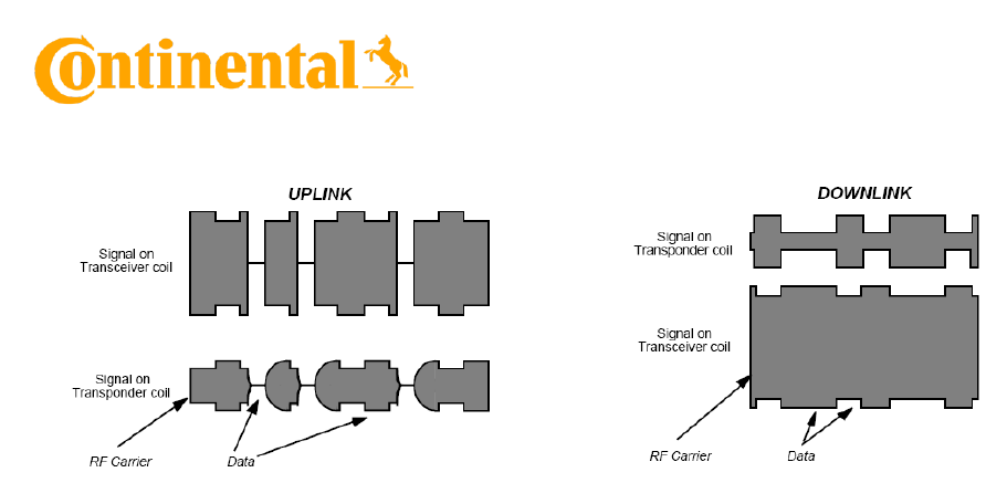
The reader provides energy to the transponder by an electromagnetic field. By modulating this field, the
reader can transmit (write) data to the transponder (uplink). The transponder will power up and return its
on-chip data to the reader (downlink).
Keller, I ID S3 AD AE 1 Page 4 23.10.2017
The microprocessor interface (µPI) connects the analog front end (AFE) with the microcontroller. The
communication between transceiver and microcontroller is made via two wires (L/Z_IN and L/Z_OUT).
L/Z_IN is the data input of LRES B2, L/Z_OUT is an open drain output which is also used as input.
In read mode (observing the messages sent by the transponder) the L/Z_OUT pin provides a digital
asynchronous signal coming from demodulator chain.
In write mode, the L_EN signal defines the operation of the microprocessor interface:
When L_EN is high (Master Mode) µPI synchronizes to transponder listening window and provides on
L/Z_OUT pin the bit clock for data which will be sent to transponder via L/Z_IN pin.
When L_EN pin is low (Slave Mode) microprocessor itself controls the communication with the
transponder. L/Z_IN pin is directly controlling internal signal MOD. Signal MOD is directly controlling the
antenna drivers. When it is high the drivers are off.
In this module, L_EN is not connected to the micro controller, pin is pulled up to the 5V supply voltage of
the immobilizer circuit. This means that the Master Mode is used exclusively.
The oscillator of base station IC is designed for usage of a 4 MHz resonator. Timer part divides the 4 MHz
clock signal down to a 125 kHz signal for antenna drivers and µP interface and provides some additional
synchronization signals for receiver chain, sampler and short circuit detector.
3 Transponder
The used transponder (STXP AES) is a read/write RF transponder. It transmits Manchester coded data to
the transceiver by modulating the amplitude of the electromagnetic field and receives data and commands
in a similar way.
The transponder is supplied by carrier of an electromagnetic field induced on the attached coil. The AC
voltage is rectified in order to provide a DC internal supply voltage. When the DC voltage crosses the
Power-On level, the transponder will enter the Standby Mode and expects commands. In Standby Mode a
continuous sequence of Listen Windows (LIW) is generated. During this time, the transponder will turn to
the Receive Mode (RM) until it receives a valid RM pattern. The transponder then expects a command to
enter the desired mode of operation.
Features:
Battery-less 125 kHz crypt transponder functionality
Figure 1: Principle of data transmission between transceiver and transponder

Keller, I ID S3 AD AE 1 Page 5 23.10.2017
True 32 bit identifier (Long ID)
Secret-Key in EEPROM (unreadable)
Free User Memory (UM)
Data transmission performed by amplitude modulation
Transmission rate for 125 kHz transponder communication: 4 kbauds
Special protected dataset storage intended for mileage counter
Lock-bits to inhibit programming
Operating temperature range -40 to +85°C
125 kHz field frequency
On chip rectifier and voltage limiter
4 Power supply
Because ANT drivers drive antenna with VDD and VSS power supply levels all variations and noise in
power supply are directly fed to antenna resonant circuit. Any supply voltage fluctuations or ripple are
transferred into antenna current fluctuations by the antenna driver transistors. This is equal to a current
modulation that results in a voltage modulation at the antenna tap point. There is no possibility for the
demodulator to distinguish this modulation from the transponder modulation (transponder signal
superimposed on antenna voltage is in the range of tens of mV). Especially in the pass band of the
demodulator filters (<10 kHz), the system is very sensitive against supply hum and ripple.
For this reason a separate linear voltage regulator is used for the immobilizer circuit. The Enable pin of this
regulator is controlled by the microcontroller. The regulator is only enabled during transponder
communication.
KL30 voltage for guaranteed immobilizer function and performance:
Minimum Operating Voltage = 6,5V
Nominal Operating Voltage = 13,5V
Maximum Operating Voltage = 17,0V
5 Technical data
Parameter
Symbol
Min
Typ
Max
Unit
Conditions
Supply
Supply Voltage Immobilizer
Module
VKL30
6,5
13,5
17,0
V
Supply Voltage LRES B2
VDD
4,5
5,0
5,5
V
Current consumption
INHIBIT OFF
IQ
10
A
VINH = 0 V;
Full temp. range
Supply current in Sleep
Mode (Quiescent current)
IDDsleep
40
A
Full temp. range
Supply current excluding
drivers current in Normal
Mode
IDDon
5
10
mA
Power on reset level
Vpor
1,4
3,6
V
Full temp. range

Keller, I ID S3 AD AE 1 Page 6 23.10.2017
AGND level
VAGND
2,35
2,5
2,65
V
Full temp. range
C interface
Input logic high
VIH
0,8 VDD
V
Full temp. range
Input logic low
VIL
0,2 VDD
V
Full temp. range
Input leakage current
IL
-1
+1
A
Full temp. range
L/Z_OUT sink current
IL/Z_OUT
2,5
mA
L/Z_OUT output logic low
VL/Z_OUT
0,4
V
Environment requirements
Ambient temperature
TA
-40
+85
°C
Junction temperature
TJ
-40
+110
°C
Package thermal resistor
Rth
69
70
71
°C/W
Antenna circuit
Carrier frequency
fANT
125
kHz
Resonant frequency
fRES
120
125
130
kHz
Antenna voltage
VCoil2
55
75
95
Vpp
LCoil = 1.041mH ± 5%,
QCoil = 8.55 ± 15%
Antenna current (RMS)
Vsense
30
34
38
mA
LCoil = 1.041mH ± 5%,
QCoil = 8.55 ± 15%
Oscillator
Oscillator frequency
fOSC
4
MHz
Antenna drivers
Output resistance
RADout
3
6
Ω
IA1=10mA
9
Ω
IA1=100mA
Full temp. range
AM demodulation
Input sensitivity
Vsense
0,85
1,42
mVpp
Full temp. range
Signal on DEMOD_IN with
no transitions on
DEMOD_OUT
VSN
140
Vpp
DEMOD_IN common mode
range
VCM
VSS
+ 0,5
VDD
- 0,5
V
DEMOD_IN input resistance
to AGND
RDI
140
200
260
kΩ
Full temp. range
100
400
kΩ

Keller, I ID S3 AD AE 1 Page 7 23.10.2017
6 Label Information USA and Canada
United States (US)
This device complies with Part 15 of the FCC Rules. Operation is subject to the
following two conditions:
(1) this device may not cause harmful interference, and
(2) this device must accept any interference received, including interference that
may cause undesired operation.
Changes or modifications not expressly approved by the party responsible for
compliance could void the user's authority to operate the equipment.
Products, which include above-mentioned module, have been approved by the Certification
process. They must have a label showing the FCC ID number:
Continental
17A920790
FCC ID:KR517A920790
CANADA
This device complies with Industry Canada licence-exempt RSS standard(s). Operation
is subject to the following two conditions: (1) this device may not cause interference, and
(2) this device must accept any interference, including interference that may cause
undesired operation of the device.
Products, which include above-mentioned module, have been approved by the certification
process. They must have a label a label showing the IC ID number:
IC:7812D-17A920790
The HVIN (Hardware Version Identification Number) identifies hardware specifications
of a product version. The HVIN replaces the ISED Model Number in the legacy E-
filing System. An HVIN is required for all products for certification applications.
HVIN: 5a

Keller, I ID S3 AD AE 1 Page 8 23.10.2017
Owner Manual:
Operation is subject to the following two conditions: (1) this device may not cause
harmful interference, and (2) this device must accept any interference received, including
interference that may cause undesired operation.
Le présent appareil est conforme aux CNR d'Industrie Canada applicables aux appareils
radio exempts de licence. L'exploitation est autorisée aux deux conditions suivantes : (1)
l'appareil ne doit pas produire de brouillage, et (2) l'utilisateur de l'appareil doit accepter
tout brouillage radioélectrique subi, même si le brouillage est susceptible d'en
compromettre le fonctionnement.