Crossbow Technology M2110 2.4 GHz ZigBee Module User Manual Installation Manual
Crossbow Technology, Inc. 2.4 GHz ZigBee Module Installation Manual
UserManual.wiki
>
Crossbow Technology
>
M2110 User Manual
Installation Manual
Navigation menu
Upload a User Manual
Namespaces
Wiki Guide
HTML
PDF
Info
Views
User Manual
Discussion / Help
Navigation


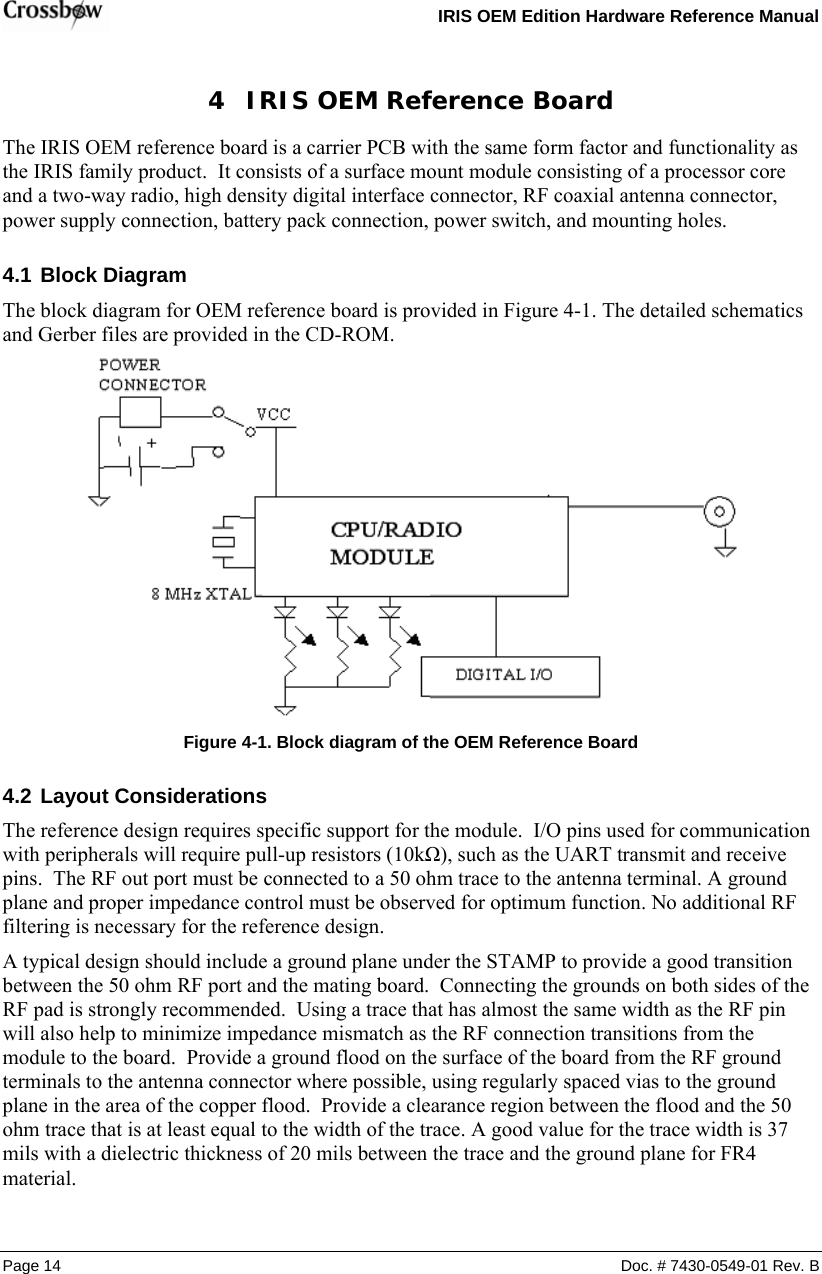
![IRIS OEM Edition Hardware Reference Manual When CKOPT is programmed, the Oscillator output will oscillate will a full rail-to-rail swing on the output. This mode is suitable when operating in a very noisy environment or when the output from XTAL2 drives a second clock buffer. This mode has a wide frequency range. When CKOPT is unprogrammed, the Oscillator has a smaller output swing. This reduces power consumption considerably. This mode has a limited frequency range and it can not be used to drive other clock buffers. C1 and C2 should always be equal for both crystals and resonators. The optimal value of the capacitors depends on the crystal or resonator in use, the amount of stray capacitance, and the electromagnetic noise of the environment. XTAL2XTAL1GNDXTAL2XTAL1GND Figure 4-3. Crystal Oscillator Connections The device has the following clock source options, selectable by Flash fuse bits as shown in Table 4-1. The clock from the selected source is input to the AVR clock generator, and routed to the appropriate modules. Table 4-1. Device Clocking Options Selection Device Clocking Option CKSEL[3..0]Low Power Crystal Oscillator 1111—1000Full Swing Crystal Oscillator 0111—0110Low-Frequency Crystal Oscillator 0101-0100 Internal 128kHz RC Oscillator 0011 Calibrated Internal RC Oscillator 0010 External Clock 0000 Some initial guidelines for choosing capacitors for use with crystals are given in Table 4-2. For ceramic resonators, the capacitor values given by the manufacturer should be used. Table 4-2. Low Power Crystal Oscillator Operating Modes CKSEL[3..1] Freq Range (MHz) Capacitor Range100† 0.4 - 0.9 - 101 0.9 – 3.0 12 – 22 pF 110 3.0 – 8.0 12 – 22 pF 111 8.0 – 16.0 12 – 22 pF † ceramic resonators only 4.3.1 Internal RC Oscillator The Calibrated Internal RC Oscillator provides a default 8.0 MHz clock. All frequencies are nominal values at 3V and 25°C. This clock may be selected as the system clock by programming the CKSEL fuses as shown in Table 4-3. If selected, it will operate with no external components. Page 16 Doc. # 7430-0549-01 Rev. B](https://usermanual.wiki/Crossbow-Technology/M2110/User-Guide-900919-Page-18.png)
![IRIS OEM Edition Hardware Reference Manual Doc. # 7430-0549-01 Rev. B Page 17 Table 4-3. Internal Calibrated RC Oscillator Operating Modes CKSEL[3..0] Nominal Freq Range (MHz)0010 7.3 – 8.1 4.3.2 System Clock Prescaler The processor has a system clock prescaler, and the system clock can be divided by setting the “Clock Prescale Register - CLKPR” as shown in Table 4-4. This feature can be used to reduce the system frequency and the power consumption when the requirement for processing power is minimized. Table 4-4.Clock Prescaler Select CLKPS[3..0] Clock Division Factor 0000 1 0001 2 0010 4 0011 8 0100 16 0101 32 0110 64 0111 128 1000 256 1001 – 1111 Reserved 4.3.3 128 kHz Internal Oscillator The 128 kHz internal Oscillator is a low power Oscillator providing a clock of 128 kHz. The frequency is nominal at 3V and 25℃. This clock maybe selected as the system clock by programming the CKSEL fuses to “11” as show in Table 4-6. Table 4-5 128 kHz Internal Oscilator Operating Modes CKSEL[3..0] Nominal Freq (kHz) 0011 128 More information is available in the datasheet for Atmel’s ATmega1281 processor. 4.4 Solder Profile 4.4.1 Hand-soldering Instructions for Hand Soldering of Crossbow OEM Module are provided below. Method 1: 1) Pre-tin the surface mount pads on the board the OEM module will be soldered to. Be careful to use an equal amount of solder on each pad.](https://usermanual.wiki/Crossbow-Technology/M2110/User-Guide-900919-Page-19.png)
![IRIS OEM Edition Hardware Reference Manual Doc. # 7430-0549-01 Rev. B Page 21 single ended voltage inputs are reference to 0V (GND). The ADC ports are high impedance inputs to the ADC, used for voltage sampling. The uppermost bits (ADC[4..7]) also support the JTAG interface. The JTAG port can be enabled by choosing that option in the fuse bits for the processor. Choosing the JTAG active option will cause approximately 50k ohms to be applied from the ADC pin to VCC. This setting can affect the accuracy of ADC readings from weak sources. Table 4-5. JTAG Pin Definitions PIN PORT ADC4 TCK ADC5 TMS ADC6 TDO ADC7 TDI RSTN RSTN The JTAG programming capability supports: • Flash programming and verifying • EEPROM programming and verifying • Fuse programming and verifying • Lock bit programming and verifying 4.5.7 GPIO The remainder of the I/O pins is available as GPIO under processor configuration control. All GPIO ports have true Read-Modify-Write functionality when used as general digital I/O ports. This means that the direction of one port pin can be changed without unintentionally changing the direction of any other pin with the SBI and CBI instructions. The same applies when changing drive value (if configured as output) or enabling/disabling of pull-up resistors (if configured as input). They can be left floating if not used, or can be set as inputs with a weak pull-up, outputs set high, or outputs set low.](https://usermanual.wiki/Crossbow-Technology/M2110/User-Guide-900919-Page-23.png)