Crossbow Technology M2110 2.4 GHz ZigBee Module User Manual Installation Manual
Crossbow Technology, Inc. 2.4 GHz ZigBee Module Installation Manual
Installation Manual

M2110 Hardware Reference Manual
Revision B, January, 2008
PN: 7430-0549-01
© 2005-2007 Crossbow Technology, Inc. All rights reserved.
Information in this document is subject to change without notice.
Crossbow, MoteWorks, IRIS, MICA, TrueMesh and XMesh are the trademarks of Crossbow
Technology, Inc. Other product and trade names are trademarks or registered trademarks of their
respective holders.

IRIS OEM Edition Hardware Reference Manual
Doc. # 7430-0549-01 Rev. B Page 1
Table of Contents
About This Document.................................................................................................................... 3
4
5
5
8
9
9
9
10
12
14
14
14
15
17
19
22
22
24
24
25
25
28
29
29
29
30
30
31
31
31
31
31
31
1 Introduction.............................................................................................................................
2 Quick Start for the OEM Kit Users......................................................................................
2.1 Out-of-the-Box Demo ......................................................................................................
3 Product Overview...................................................................................................................
3.1 Block Diagram and Schematics for the OEM Edition Module ......................................
3.2 Electrical Specifications...................................................................................................
3.3 Environmental Specifications ..........................................................................................
3.4 Mechanical Dimensions.................................................................................................
3.5 Pin-out Description ........................................................................................................
4 IRIS OEM Reference Board................................................................................................
4.1 Block Diagram ...............................................................................................................
4.2 Layout Considerations ...................................................................................................
4.3 Circuit Design Considerations.......................................................................................
4.4 Solder Profile..................................................................................................................
4.5 Peripheral Interfaces on OEM Edition Module.............................................................
5 Power .....................................................................................................................................
5.1 Battery Power.................................................................................................................
6 Radios.....................................................................................................................................
6.1 M2110.............................................................................................................................
7 Antennas................................................................................................................................
7.1 Radio/Antenna Considerations ......................................................................................
8 Flash Data Logger and Serial ID Chip...............................................................................
9 Atmega1281 Fuses ................................................................................................................
9.1 JTAG fuse.......................................................................................................................
9.2 Using UISP to set fuses..................................................................................................
10 Sensor Boards & Expansion Connectors.........................................................................
10.1 Sensor Board Compatibility via Expansion Connector.............................................
11 USB Programming Pod.....................................................................................................
11.1 ISP...............................................................................................................................
11.2 Mote Programming Using the MIB520 .....................................................................
11.3 MIB520 USB Drivers.................................................................................................
11.4 Power ..........................................................................................................................
11.5 USB Interface .............................................................................................................

IRIS OEM Edition Hardware Reference Manual
Page 2 Doc. # 7430-0549-01 Rev. B
11.6 Programming Interface............................................................................................... 32
33
33
33
33
34
12 Appendix A. Warranty and Support Information..........................................................
12.1 Customer Service........................................................................................................
12.2 Contact Directory .......................................................................................................
12.3 Return Procedure ........................................................................................................
12.4 Warranty .....................................................................................................................
IRIS OEM Edition Hardware Reference Manual
About This Document
The following annotations have been used to provide additional information.
; NOTE
Note provides additional information about the topic.
; EXAMPLE
Examples are given throughout the manual to help the reader understand the terminology.
3 IMPORTANT
This symbol defines items that have significant meaning to the user
WARNING
The user should pay particular attention to this symbol. It means there is a chance that physical
harm could happen to either the person or the equipment.
The following paragraph heading formatting is used in this manual:
1 Heading 1
1.1 Heading 2
1.1.1 Heading 3
This document also uses different body text fonts (listed in Table 0-1) to help you distinguish
between names of files, commands to be typed, and output coming from the computer.
Table 0-1. Font types used in this document.
Font Type Usage
Courier New Normal Sample code and screen output
Courier New Bold Commands to be typed by the user
Times New Roman Italic TinyOS files names, directory names
Franklin Medium Condensed Text labels in GUIs
Doc. # 7430-0549-01 Rev. B Page 3

IRIS OEM Edition Hardware Reference Manual
Page 4 Doc. # 7430-0549-01 Rev. B
1 Introduction
This User’s Manual describes the hardware features of the OEM Edition M2110 modules.
Table 1-1 below lists the models covered in this Manual.
Table 1-1. OEM Edition Models covered in the Reference Manual
Model Number Description
M2110 2.4GHz IRIS OEM module
This Manual is not a software guide to programming the Motes using MoteWorks, nor is it a
guide to pre-built software packages that run on top of the Motes. The following resources are
available regarding software:
MoteWorks Getting Started Guide by Crossbow Technology, Inc.
XMesh User’s Manual by Crossbow Technology, Inc.
MoteView User’s Manual by Crossbow Technology, Inc.
MoteConfig User’s Manual by Crossbow Technology, Inc.

IRIS OEM Edition Hardware Reference Manual
Doc. # 7430-0549-01 Rev. B Page 5
2 Quick Start for the OEM Kit Users
3 IMPORTANT: This section is intended for the Standard OEM Edition module kit users
only. If you did not purchase the complete pre-programmed kit, but only stand-alone boards then
skip to Chapter 3.
2.1 Out-of-the-Box Demo
This section will step you through the process of setting up a simple Mote sensor network
demonstration. The four main steps are to
1. Install MoteView on your Windows PC
2. Install the USB drivers for the MIB520 programming pod
3. Set up OEM reference Motes with the MDA300 sensor boards
4. Start MoteView and log sensor data from the wireless network
2.1.1 Installing MoteView on a Windows PC
Before you can use MoteView you have to install it on a PC. The requirements necessary to
properly install MoteView are below:
1. A PC with one of the following operating systems
• Windows XP Home/Professional
• Windows 2000 with SP4
2. An NTFS file system
3. Screen resolution must be at least 800 × 600 or the interface will require scrollbars
4. Administrative privileges to write to Windows registry
; NOTE: Prior to installing MoteView, it is highly recommended that you shut down all the
programs running on your computer.
Follow these installation steps:
1. Insert the WSN Kit CDROM into the computer’s CD drive.
2. Double-click on MoteViewSetup_<version>.exe from “MoteView” folder.
3. Select the desired installation directory (the default installation directory is C:\Program
Files\Crossbow\MoteView)
4. Select all available installation tasks
5. InstallShield will guide you through the rest of the process and install the following:
• MoteView application
• PostgreSQL 8.0 database service
• PostgreSQL ODBC driver
• Microsoft .NET framework

IRIS OEM Edition Hardware Reference Manual
Page 6 Doc. # 7430-0549-01 Rev. B
2.1.2 Installing the USB drivers for the MIB520 Programming Pod
When you plug an MIB520 into your PC for the first time, Windows detects and reports it as
new hardware. Do the following steps.
1. Connect one end of the USB extension cable to an available USB port on your PC.
Connect the other to the MIB520’s USB connector. In a few moments your PC will
identify the MIB520 as a new hardware.
2. When the PC directs you to search for a suitable driver select “Install from a list or
specific location (Advanced).”
3. Browse to “MIB520 Drivers” folder of the MoteWorks Support Tools CDROM.
4. Follow the FTDI InstallShield Wizard through the rest of the installation process. Up to
four different installations will take place.
When the drivers are installed, you will see two serial ports associated with the MIB520. Before
programming or listening to Motes using the MIB520, you need to see which ports were
assigned to the MIB520. To find out do the following:
5. Click on Start > Control Panel > System > Hardware > Device Manager > Ports (COM & LPT).
6. Make a note of the assigned COM port numbers.
; NOTE: The two virtual serial ports for MIB520 are com<x> and com<x+1>
com<x> is for Mote programming, and
com<x+1> is for Mote communication.
2.1.3 Setting up the OEM Reference Motes with the XMDA300 Board
1. The OEM reference Motes are numbered from 0 to 3. Identify the Motes labeled one
(“1”) through three (“3”). Attach the MDA300 boards to each of these to Motes via the
mating 51-pin connectors. Turn the Motes on by putting the switch at SW2 to “ON.”
(Remember to install two of the AA alkaline batteries included in your kit.)
2. Identify the OEM reference Mote labeled as number zero (“0”) and attach it to the
MIB520 programming pod via the mating 51-pin adapter.
2.1.4 Setting up MoteView
All the visualization tools in MoteView require being connected to a database. The database is in
your PC (“localhost”), but can also be a remote PC/server. Instructions for logging and viewing
data locally are described next.
1. Start MoteView by double-clicking the icon on the desktop.
2. Open the Connection Wizard window from the menu File > Connect > Connect to WSN.
3. Select the Mode tab, check on Acquire Live Data as operation mode and Local as acquisition
type and click on Next >>.
4. In the Gateway tab, select MIB520 as the interface board, and change the Serial Port port
to the higher of the two com numbers assigned to the MIB520 during the driver
installation. For example if the COM ports on the MIB520 are COM8 and COM9, then
select in COM9 from the Serial Port drop-down box. Select the “57600” for the Baud rate
from drop-down box and click on Next >>.
IRIS OEM Edition Hardware Reference Manual
5. In the Sensor Board tab, for the Application Name, select “XMDA300” from the pull-down
menu.
6. Click on the DONE button.
Soon after that it should display incoming data. Click on the MoteView window to view data,
time plots of sensor values, and topology of the Mote network.
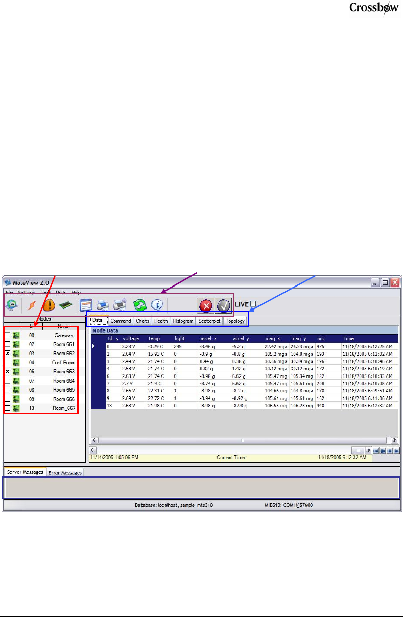
2.1.5 User Interfaces
You should see nodes one, two and three appear in the node list on the left hand side of the
MoteView window. MoteView has four main user interface sections which you can browse and
use.
• Toolbar / Menus: Allows the user to specify actions and initiate command dialogs.
• Node List: Shows all known nodes in a deployment and health status summary.
• Visualization Tabs: Enables the user to view the sensor data in various ways.
• Server Messages: Displays a log of server events and incoming messages.
Server Messages
Toolbar/Menus Visualization Tabs Node List
Figure 2-1. Screenshot of the MoteView GUI
More information about MoteView and its features can be found in the MoteView User’s manual.
Doc. # 7430-0549-01 Rev. B Page 7
IRIS OEM Edition Hardware Reference Manual
3 Product Overview
Crossbow’s M2110 OEM Edition module provides users with high level functional integration
designed to optimize the addition of wireless mesh networking technology to a wide variety of
both new and existing custom sensing applications. Powerful new design features include:
• Optimized processor/radio module integration based on Crossbow’s extensive Mote
development and deployment.
• Flexible onboard hardware interface for both standard and custom sensing devices.
• Comprehensive software support, including sensor board drivers and algorithms, via
Crossbow’s industry leading MoteWorks software platform.
The M2110 OEM Edition module is the functional equivalent of Crossbow’s newest generation
IRIS family Mote in a postage stamp form factor. This inherent design continuity makes the
OEM Edition module an ideal solution for next-generation mesh networking products and
designs.
By utilizing open-platform, standards based interfaces the OEM Edition module offers users an
attractive value proposition consisting of easily differentiated, low-power radio/processor
modules that can be rapidly designed and built.
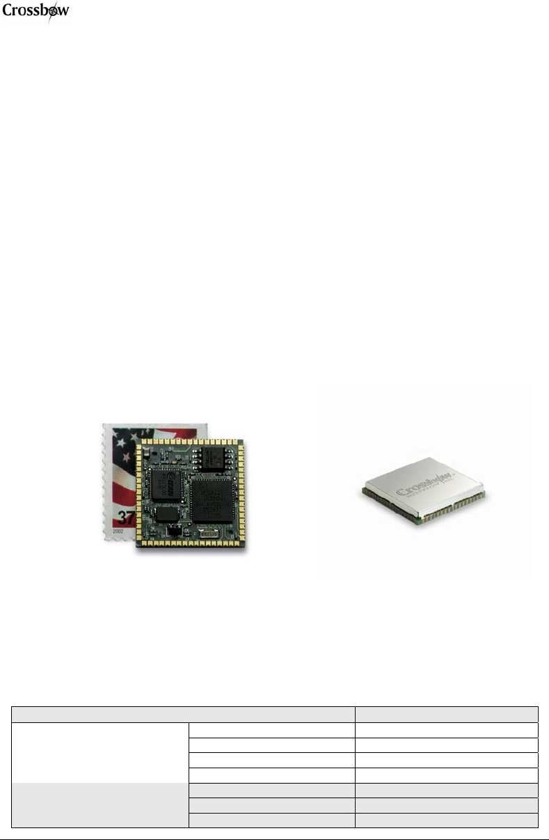
Figure 3-1. Photo of the OEM Edition Module
The Table 3-1 below summarizes the main features of OEM Edition modules.
Table 3-1. OEM Edition Module Product Summary
Mote Hardware Platform M2110
Chip ATMegal1281V
Type 7.37 MHz, 8 bit
MCU Program Memory (kB) 128
SRAM (kB) 8
10-Bit ADC 0 V to 3 V input
UART 2
Sensor Board Interface
Other interfaces DIO, I2C
Page 8 Doc. # 7430-0549-01 Rev. B
IRIS OEM Edition Hardware Reference Manual
Chip AT86RF230
Radio Frequency (MHz) 2400
RF Transceiver (Radio)
TMax. Data Rate (kbits/sec)T 250
Chip AT45DB041D
Connection Type SPI
Flash Data Logger Memory
Size (kB) 512
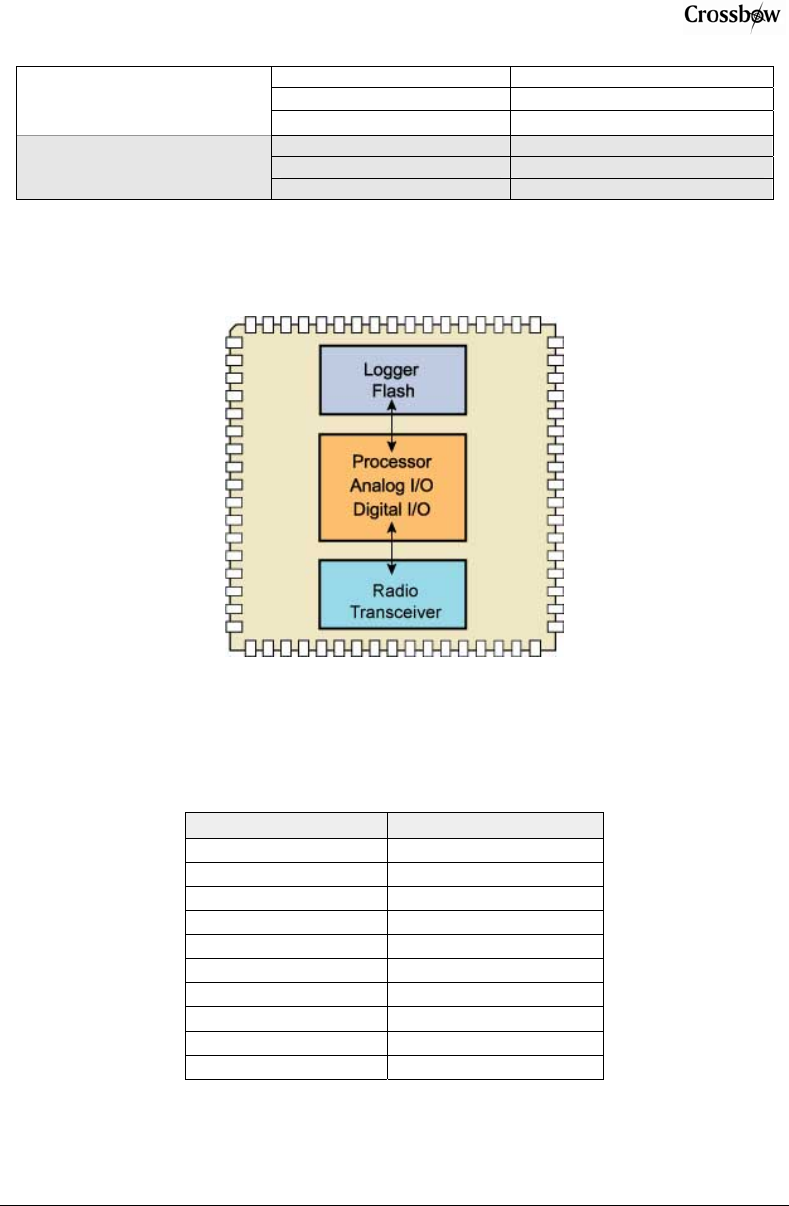
3.1 Block Diagram and Schematics for the OEM Edition Module
Figure 3-2. Block Diagram for the OEM Edition Module
3.2 Electrical Specifications
The electrical specifications for the OEM Edition module are provided in Table 3-2.
Table 3-2. M2110 Electrical Specifications
Parameter Operating Value
Power supply 2.7 to 3.6 Volts
I/O See Table 3-4
GPIO levels 0 - VCC
GPIO current (source/sink) 10 mA max
UART levels 0 - VCC
UART data rate Up to 115kB
I2C rate 100 kbps max
I2C levels 0 - VCC
Interrupt levels 0 - VCC
RF port 50 ohm
3.3 Environmental Specifications
The environmental specifications for the OEM Edition module are provided in Table 3-3.
Doc. # 7430-0549-01 Rev. B Page 9
IRIS OEM Edition Hardware Reference Manual
Table 3-3. M2110 Environmental Specifications
Parameter Operating Value
Storage Temperature -40 deg. C to + 85 deg. C
Operating Temperature -40 deg. C to + 85 deg. C
Shock 6g any axis
Vibration 2g random any axis
Humidity 0 to 90 % RH
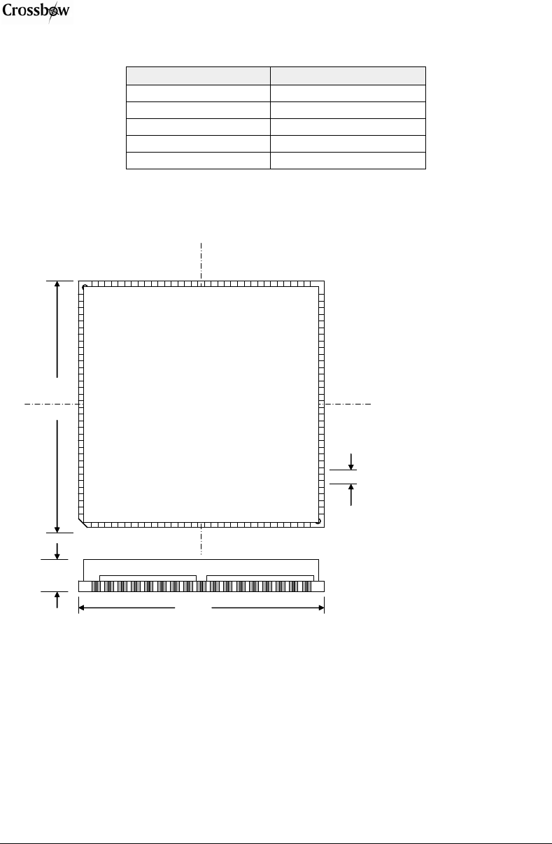
3.4 Mechanical Dimensions
Page 10 Doc. # 7430-0549-01 Rev. B
Figure 3-3. Mechanical Outline Drawing of OEM Edition Module
e = 0.050 INCH
NO. CONTACTS = 68
L
117
COMPONENT
SIDE
w
18
3452
68
THICKNESS = 0.062 INCH
COPLANARITY = 0.003 INCH
W = L = 0.944 TO 0.964 INCH
3551
H
H = 0.161 TO 0.200 INCH
e
MATERIAL = FR4
e = 0.050 INCH
NO. CONTACTS = 68
L
117
COMPONENT
SIDE
w
18
3452
68
THICKNESS = 0.062 INCH
COPLANARITY = 0.003 INCH
W = L = 0.944 TO 0.964 INCH
3551
H
H = 0.161 TO 0.200 INCH
e
MATERIAL = FR4
IRIS OEM Edition Hardware Reference Manual
Doc. # 7430-0549-01 Rev. B Page 11
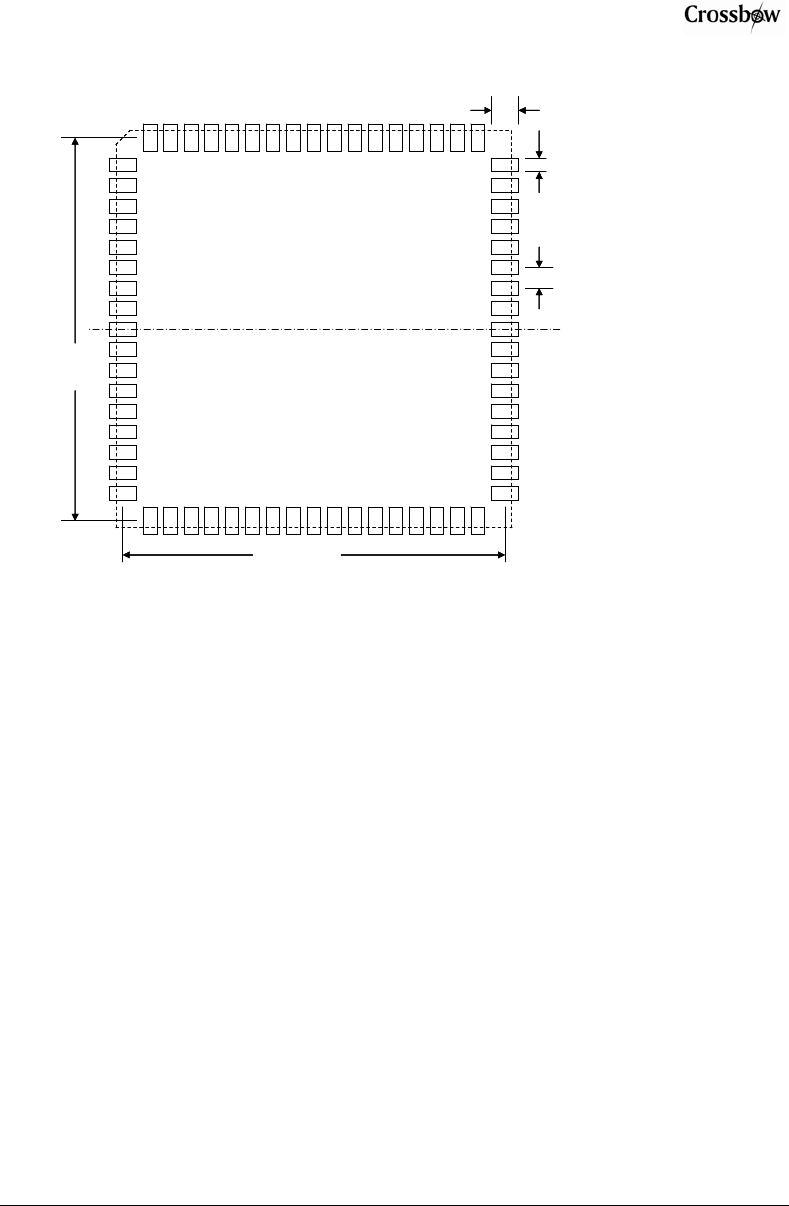
Figure 3-4. Recommended Land Pattern for OEM Edition Module
0.031(0.80)
0.083(2.10)
0.050(1.27)
0.925(23.5)
0.925(23.5)
DIMENSIONS IN INCHES (MM)
0.031(0.80)
0.083(2.10)
0.050(1.27)
0.925(23.5)
0.925(23.5)
DIMENSIONS IN INCHES (MM)

IRIS OEM Edition Hardware Reference Manual
Page 12 Doc. # 7430-0549-01 Rev. B
3.5 Pin-out Description
The 68-pin interface provides a user interface for power and ground, power control of peripheral
sensors, ADC inputs for reading sensor outputs, a UART interface, and I2C interface, general
purpose digital IO, and others.
Table 3-4. Pin-out description for OEM Edition Module
Pin Name Description Pin Name Description
1 GND Ground 35 GND Ground
2 PG0 GPIO 36 FLASH_RSTN Flash Reset
3 PG1 GPIO 37 FLASH_CS Flash Chip Select
4 PG2 GPIO 38 TC2 GPIO
5 XLT2 External Crystal 39 PG5 GPIO
6 XLT1 External Crystal 40 NC Not Connected
7 I2C_CLK I2C Bus Clock 41 NC Not Connected
8 I2C_DATA I2C Bus Data 42 GND RF Ground
9 ONE_WIRE One Wire 43 RF_OUT RF Output
10 UART0_RX UART0 Receive 44 GND RF Ground
11 UART0_TX UART0 Transmit 45
TR NC
12 SPI_CK SPI Serial Clock 46 NC Not Connected
13 RSTN Reset 47 NC Not Connected
14 USART1_TX UART1 Transmit 48 NC Not Connected
15 USART1_RX UART1 Receive 49 NC Not Connected
16 USART1_CK UART1 Clock 50 NC Not Connected
17 DVCC Digital Supply 51 AVCC Analog Supply
18 GND Ground 52 GND Ground
19 PW0 GPIO/PWM 53 LED3 Yellow LED
20 PW1 GPIO/PWM 54 LED2 Green LED
21 PW2 GPIO/PWM 55 LED1 Red LED
22 PW3 GPIO/PWM 56 INT7 GPIO
23 PW4 GPIO/PWM 57 INT6 GPIO
24 PW5 GPIO/PWM 58 INT5 GPIO
25 PW6 GPIO/PWM 59 INT4 GPIO
26 PW7 GPIO/PWM 60 ADC7 ADC Channel 7
27 PB4 PWM0 61 ADC6 ADC Channel 6
28 PB5 PWM1A 62 ADC5 ADC Channel 5
29 PB6 PWM1B 63 ADC4 ADC Channel 4
30 PE2 GPIO 64 ADC3 ADC Channel 3
31 PE3 GPIO 65 ADC2 ADC Channel 2
32 PA7 GPIO 66 ADC1 ADC Channel 1
33 PB7 NC 67 ADC0 ADC Channel 0
34 AVCC Analog Supply 68 DVCC Digital Supply

IRIS OEM Edition Hardware Reference Manual
117
COMPONENT
SIDE
18
34
3551
52
68 GND
GND
PG0
PG1
PG2
XTL2
XTL1
I2C_CLK
I2C_DATA
ONE_WIRE
UART0_RX
UART0_TX
SPI_CK
RSTN
USART1_TX
USART1_RX
USART1_CK
DVCC
PW0
PW1
PW2
PW3
PW4
PW5
PW6
PW7
PB4
PB5
PB6
PE2
PE3
PA7
PB7
AVCC
AVCC
NC
NC
HPA
LNA
RF_TR
GND
RF_OUT
GND
NC
NC
FLASH_CS
FLASH_RS
GND
CC
C0
C1
C2
C3
C4
C5
C6
C7
4
5
6
7
D1
D2
D3
D
TN
DV
AD
AD
AD
AD
AD
AD
AD
AD
INT
INT
INT
INT
LE
LE
LE
GN
117
COMPONENT
SIDE
18
34
3551
52
68 GND
GND
PG0
PG1
PG2
XTL2
XTL1
I2C_CLK
I2C_DATA
ONE_WIRE
UART0_RX
UART0_TX
SPI_CK
RSTN
USART1_TX
USART1_RX
USART1_CK
DVCC
PW0
PW1
PW2
PW3
PW4
PW5
PW6
PW7
PB4
PB5
PB6
PE2
PE3
PA7
PB7
AVCC
AVCC
NC
NC
HPA
LNA
RF_TR
GND
RF_OUT
GND
NC
NC
PG5
TC2
FLASH_CS
FLASH_RS
GND
CC
C0
C1
C2
C3
C4
C5
C6
C7
4
5
6
7
D1
D2
D3
D
TN
DV
AD
AD
AD
AD
AD
AD
AD
AD
INT
INT
INT
INT
LE
LE
LE
GN
NC
Figure 3-5. Pin-out Diagram for OEM Edition Module
Doc. # 7430-0549-01 Rev. B Page 13
IRIS OEM Edition Hardware Reference Manual
4 IRIS OEM Reference Board
The IRIS OEM reference board is a carrier PCB with the same form factor and functionality as
the IRIS family product. It consists of a surface mount module consisting of a processor core
and a two-way radio, high density digital interface connector, RF coaxial antenna connector,
power supply connection, battery pack connection, power switch, and mounting holes.
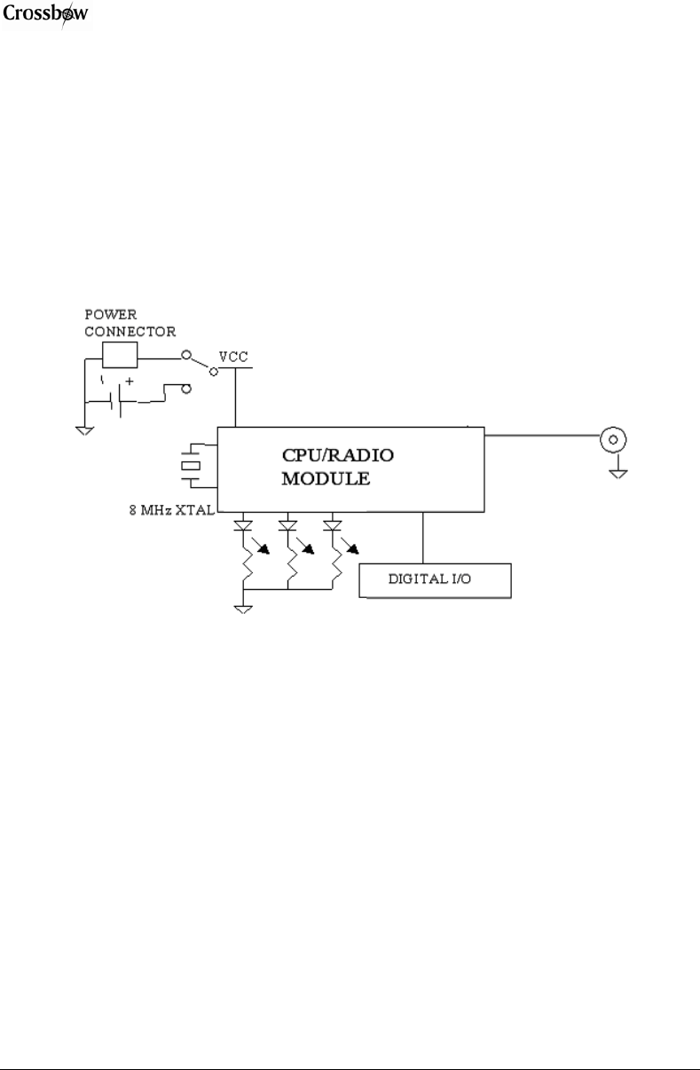
4.1 Block Diagram
The block diagram for OEM reference board is provided in Figure 4-1. The detailed schematics
and Gerber files are provided in the CD-ROM.
Figure 4-1. Block diagram of the OEM Reference Board
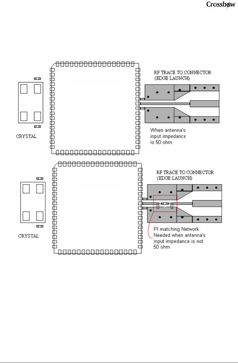
4.2 Layout Considerations
The reference design requires specific support for the module. I/O pins used for communication
with peripherals will require pull-up resistors (10kΩ), such as the UART transmit and receive
pins. The RF out port must be connected to a 50 ohm trace to the antenna terminal. A ground
plane and proper impedance control must be observed for optimum function. No additional RF
filtering is necessary for the reference design.
A typical design should include a ground plane under the STAMP to provide a good transition
between the 50 ohm RF port and the mating board. Connecting the grounds on both sides of the
RF pad is strongly recommended. Using a trace that has almost the same width as the RF pin
will also help to minimize impedance mismatch as the RF connection transitions from the
module to the board. Provide a ground flood on the surface of the board from the RF ground
terminals to the antenna connector where possible, using regularly spaced vias to the ground
plane in the area of the copper flood. Provide a clearance region between the flood and the 50
ohm trace that is at least equal to the width of the trace. A good value for the trace width is 37
mils with a dielectric thickness of 20 mils between the trace and the ground plane for FR4
material.
Page 14 Doc. # 7430-0549-01 Rev. B
IRIS OEM Edition Hardware Reference Manual
The RF output port is 50 ohm and can be connected directly to a 50 ohm microstrip or 50 ohm
coaxial cable. A PI-Matching network is recommended for antenna matching especially when
using inner antennas. If the antenna’s input impedance is not 50 ohm, please contact antenna
vendor and ask for matching network value.
An example of a typical layout is shown in Figure 4-2.
OEM Module
OEM Module
Figure 4-2. An example layout for OEM Edition Module
4.3 Circuit Design Considerations
An external crystal is not required. The unit can be configured to run on the internal RC
oscillator, leaving the crystal connections open. If an external crystal is to be used, place the
crystal as close to the input pins as possible to reduce parasitics. When selecting capacitors for
the crystal, take into account the stray capacitance from the board to the module and adjust
accordingly. If an external clock is used, XTL1 (PIN 6) should be used, and XTL2 (PIN 5)
should be left open. For proper operation, correct selection of clock fuse options is required.
XTAL1 and XTAL2 are input and output, respectively, of an inverting amplifier which can be
configured for use as an On-chip Oscillator, as shown in Figure 4-3. Either a quartz crystal or a
ceramic resonator may be used. Normally, a 7.3728 MHz crystal is used for units requiring serial
communication. The CKOPT fuse selects between two different Oscillator Amplifier modes.
Doc. # 7430-0549-01 Rev. B Page 15
IRIS OEM Edition Hardware Reference Manual
When CKOPT is programmed, the Oscillator output will oscillate will a full rail-to-rail swing on
the output. This mode is suitable when operating in a very noisy environment or when the output
from XTAL2 drives a second clock buffer. This mode has a wide frequency range. When
CKOPT is unprogrammed, the Oscillator has a smaller output swing. This reduces power
consumption considerably. This mode has a limited frequency range and it can not be used to
drive other clock buffers.
C1 and C2 should always be equal for both crystals and resonators. The optimal value of the
capacitors depends on the crystal or resonator in use, the amount of stray capacitance, and the
electromagnetic noise of the environment.
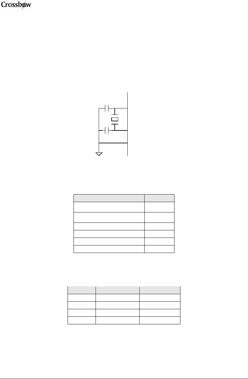
XTAL2
XTAL1
GND
XTAL2
XTAL1
GND
Figure 4-3. Crystal Oscillator Connections
The device has the following clock source options, selectable by Flash fuse bits as shown in
Table 4-1. The clock from the selected source is input to the AVR clock generator, and routed to
the appropriate modules.
Table 4-1. Device Clocking Options Selection
Device Clocking Option CKSEL[3..0]
Low Power Crystal Oscillator 1111—1000
Full Swing Crystal Oscillator 0111—0110
Low-Frequency Crystal Oscillator 0101-0100
Internal 128kHz RC Oscillator 0011
Calibrated Internal RC Oscillator 0010
External Clock 0000
Some initial guidelines for choosing capacitors for use with crystals are given in Table 4-2. For
ceramic resonators, the capacitor values given by the manufacturer should be used.
Table 4-2. Low Power Crystal Oscillator Operating Modes
CKSEL[3..1] Freq Range (MHz) Capacitor Range
100†
0.4 - 0.9 -
101 0.9 – 3.0 12 – 22 pF
110 3.0 – 8.0 12 – 22 pF
111 8.0 – 16.0 12 – 22 pF
† ceramic resonators only
4.3.1 Internal RC Oscillator
The Calibrated Internal RC Oscillator provides a default 8.0 MHz clock. All frequencies are
nominal values at 3V and 25°C. This clock may be selected as the system clock by programming
the CKSEL fuses as shown in Table 4-3. If selected, it will operate with no external components.
Page 16 Doc. # 7430-0549-01 Rev. B

IRIS OEM Edition Hardware Reference Manual
Doc. # 7430-0549-01 Rev. B Page 17
Table 4-3. Internal Calibrated RC Oscillator Operating Modes
CKSEL[3..0] Nominal Freq Range (MHz)
0010 7.3 – 8.1
4.3.2 System Clock Prescaler
The processor has a system clock prescaler, and the system clock can be divided by setting the
“Clock Prescale Register - CLKPR” as shown in Table 4-4. This feature can be used to reduce
the system frequency and the power consumption when the requirement for processing power is
minimized.
Table 4-4.Clock Prescaler Select
CLKPS[3..0] Clock Division Factor
0000 1
0001 2
0010 4
0011 8
0100 16
0101 32
0110 64
0111 128
1000 256
1001 – 1111 Reserved
4.3.3 128 kHz Internal Oscillator
The 128 kHz internal Oscillator is a low power Oscillator providing a clock of 128 kHz. The
frequency is nominal at 3V and 25℃. This clock maybe selected as the system clock by
programming the CKSEL fuses to “11” as show in Table 4-6.
Table 4-5 128 kHz Internal Oscilator Operating Modes
CKSEL[3..0] Nominal Freq (kHz)
0011 128
More information is available in the datasheet for Atmel’s ATmega1281 processor.
4.4 Solder Profile
4.4.1 Hand-soldering
Instructions for Hand Soldering of Crossbow OEM Module are provided below.
Method 1:
1) Pre-tin the surface mount pads on the board the OEM module will be soldered to. Be
careful to use an equal amount of solder on each pad.
IRIS OEM Edition Hardware Reference Manual
2) Apply a small amount of flux to the tinned pads.
3) Place the OEM module on the pads, making sure to have the pin one reference markings
aligned. Inspect the placement to make sure the OEM module edge contacts are centered
on the pads on all four sides.
4) While applying mild pressure to the top of the OEM module (to hold it in position), apply
heat from a fine soldering tip to the area of the pre-tinned pad that is exposed at the edge
of the OEM module. Reflow only one corner pad first, and verify the OEM module is
still positioned correctly on the remaining pads.
5) Using a fine solder tip, reflow each of the pre-tinned pads until the solder flows and
makes contact with the pad on the underside of the OEM module.
Method 2:
1) Pre-tin the surface mount pads on the board the OEM module will be soldered to. Be
careful to use an equal amount of solder on each pad.
2) Apply a small amount of flux to the tinned pads.
3) Place the OEM module on the pads, making sure to have the pin one reference markings
aligned. Inspect the placement to make sure the OEM module edge contacts are centered
on the pads on all four sides.
4) While applying mild pressure to the top of the OEM module (to hold it in position), apply
heat from a thermal heat gun to the edges of the OEM module until the exposed solder on
the pre-tinned pads melts.
4.4.2 Machine Soldering
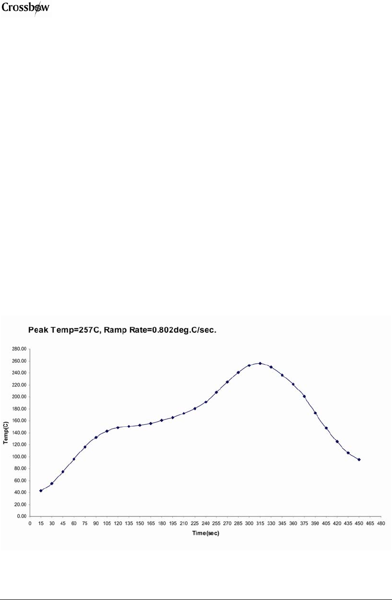
The recommended solder profile for OEM module is shown in Figure 4-4.
Figure 4-4. Recommended Temperature Profile for OEM Edition Module
Page 18 Doc. # 7430-0549-01 Rev. B

IRIS OEM Edition Hardware Reference Manual
4.5 Peripheral Interfaces on OEM Edition Module
The ports available on the OEM Edition module consist of the following:
• UART0
• USART1
• I2C bus
• SPI bus
• ONE-WIRE
• ADC ports
• GPIO
4.5.1 UART0
The UART0 port is a dual function port. It is used in conjunction with the RSTN (active LOW)
and SPI_CK lines to program the CPU. The CPU is in program mode if the RSTN line is low,
and data is clocked in using the UART0_RX and SPI_CK lines. The RSTN line has an internal
10K pull-up to bring it out of reset when power is applied. When the device is not being
programmed, the UART0 port serves as the main communication port to a system controller. An
external 10k pull-up resistor is recommended on the UART0_RX and UART0_RX ports to hold
the lines in a known state during power-up and reset. The rates supported are a function of the
system clock chosen.
; EXAMPLE
For standard crystal and resonator frequencies, the most commonly used baud rates for
asynchronous operation can be generated by using the UBRR settings as shown in Table 4-4.
UBRR values which yield an actual baud rate differing less than 0.5% from the target baud rate,
are bold in the table. Higher error ratings are acceptable, but the receiver will have less noise
resistance when the error ratings are high, especially for large serial frames. The error values are
calculated using the following equation:
Doc. # 7430-0549-01 Rev. B Page 19
100*1(%) ⎟
⎠
⎞
⎜
⎝
⎛−= BaudRate
BaudRate
Error chClosestMat
Table 4-4. Oscillator frequency = 7.32826 MHz

IRIS OEM Edition Hardware Reference Manual
Baud Rate
(bps) U2X = 0
UBRR U2X = 0
ERROR U2X = 1
UBRR U2X = 1
ERROR
2400 191 0.0% 383 0.0%
4800 95 0.0% 191 0.0%
9600 47 0.0% 95 0.0%
14.4k 31 0.0% 63 0.0%
19.2k 23 0.0% 47 0.0%
28.8k 15 0.0% 31 0.0%
38.4k 11 0.0% 23 0.0%
57.6k 7 0.0% 15 0.0%
76.8k 5 0.0% 11 0.0%
115.2k 3 0.0% 7 0.0%
4.5.2 UART1
USART1 is a shared interface, used for communication with the on-board serial flash, as well as
external serial peripherals. Proper management of the chip select lines (FLASH_CS) is required
to avoid port contention. The serial flash also has a reset line (FLASH_RSTN) that can be
asserted externally to place the serial flash in a known state. The flash reset line has an internal
10K pull-up resistor to enable the device after power-on. Additional pull-up resistors may be
required on the USART1_TX, USART1_RX, and USART_CK lines to avoid unintentional
communication with external peripherals during reset or power-on.
4.5.3 I2C
The I2C bus is a two-wire interface that is meant to control I2C peripherals. I2C peripherals
usually require an external 5K pull-up to supply power to the port, and use an addressing scheme
that is internal to the I2C peripheral. Many of the I2C peripherals have an internal hard-wired
portion of their address along with some external address decode lines in the event multiple
devices of the same kind are attached to the bus. See the individual vendor datasheets for details.
4.5.4 SPI
The SPI bus is a bidirectional synchronous bus common to many devices available. As it is
applied in the OEM Edition module, the SPI bus is dedicated to the radio data interface, and
cannot be used for other peripherals. The SPI_CK line is made available to facilitate
reprogramming the processor, and should be left in a high impedance state when not in
programming mode.
4.5.5 One-Wire
The One-Wire bus is a single wire bidirectional bus used to communicate with the Dallas/Maxim
series of One-Wire peripherals. These devices require a 5k resistor to VCC to bias the pin, and
accurate timing of signals on the bus for proper communication.
WARNING: The choice of system clock is critical to making this interface work.
4.5.6 ADC Ports
The OEM Edition module features 10-bit successive approximation ADC. The ADC is
connected to an 8-channel Analog Multiplexer which allows 8 single-ended voltage inputs. The
Page 20 Doc. # 7430-0549-01 Rev. B

IRIS OEM Edition Hardware Reference Manual
Doc. # 7430-0549-01 Rev. B Page 21
single ended voltage inputs are reference to 0V (GND). The ADC ports are high impedance
inputs to the ADC, used for voltage sampling. The uppermost bits (ADC[4..7]) also support the
JTAG interface. The JTAG port can be enabled by choosing that option in the fuse bits for the
processor. Choosing the JTAG active option will cause approximately 50k ohms to be applied
from the ADC pin to VCC. This setting can affect the accuracy of ADC readings from weak
sources.
Table 4-5. JTAG Pin Definitions
PIN PORT
ADC4 TCK
ADC5 TMS
ADC6 TDO
ADC7 TDI
RSTN RSTN
The JTAG programming capability supports:
• Flash programming and verifying
• EEPROM programming and verifying
• Fuse programming and verifying
• Lock bit programming and verifying
4.5.7 GPIO
The remainder of the I/O pins is available as GPIO under processor configuration control. All
GPIO ports have true Read-Modify-Write functionality when used as general digital I/O ports.
This means that the direction of one port pin can be changed without unintentionally changing
the direction of any other pin with the SBI and CBI instructions. The same applies when
changing drive value (if configured as output) or enabling/disabling of pull-up resistors (if
configured as input). They can be left floating if not used, or can be set as inputs with a weak
pull-up, outputs set high, or outputs set low.

IRIS OEM Edition Hardware Reference Manual
Page 22 Doc. # 7430-0549-01 Rev. B
5 Power
5.1 Battery Power
M2110 is designed for battery power. Any battery combination (AA, AAA, C, D, etc., cells) can
be used provided that the output is between 2.7 VDC to 3.6 VDC.
Care should be used in selecting the battery and its capacity to match the energy needs of the
motes and their required operating span. Also make sure that the temperature range and
associated capacity degradation are looked at prior to deployment.
Table 5-1 below provides some useful guidance on current consumption of various system
components.
Table 5-1. Current Requirements for the Motes under Various Operation
Operating Mode M2110
Current (mA)
ATMega1281V, full operation 6 (7.37 MHz)
ATMega1281V, sleep 0.010
Radio, receive 16
Radio, transmit (1 mW power) 17
Radio, sleep 0.001
Serial flash memory, write 15
Serial flash memory, read 4
Serial flash memory, sleep 0.002

IRIS OEM Edition Hardware Reference Manual
Doc. # 7430-0549-01 Rev. B Page 23
The Table 5-2 below provides some useful guidance on how to predict battery life.
Table 5-2. Estimate of battery life operation for OEM Edition Module
SYSTEM SPECIFICATIONS
Currents
Processor Example Duty
Cycle
Current (full operation) 6 mA 1
Current sleep 10 μA 99
Radio
Current in receive 16 mA 0.75
Current transmit 17 mA 0.25
Current sleep 1 μA 99
Logger Memory
Write 15 mA 0
Read 4 mA 0
Sleep 2 μA 100
Sensor Board
Current (full operation) 5 mA 1
Current sleep 5 μA 99
Computed mA-hr used each hour
Processo
r
0.0699
Radio 0.1635
Logger Memory 0.0020
Sensor Board 0.0550
Total current (mA-hr) used 0.2904
Computed battery life vs. battery size
Battery Capacity (mA-hr) Battery Life
(months)
250 1.20
1000 4.78
3000 14.35
; NOTE: In most applications, the processor and radio run for a brief period of time, followed by a
sleep cycle. During sleep, current consumption is in the micro-amps as opposed to milli-amps. This
results in very low-current draw the majority of the time, and short duration spikes while processing,
receiving, and transmitting data. This method extends battery life; however, due to the current surges, it
reduces specified battery capacity. Battery capacity is typically specified by the manufacturer for a
constant nominal current drawn.

IRIS OEM Edition Hardware Reference Manual
Page 24 Doc. # 7430-0549-01 Rev. B
6 Radios
6.1 M2110
The radio used by the M2110 is an IEEE 802.15.4 compliant RF transceiver designed for low-
power and low-voltage wireless applications. It uses Atmel’s AT86RF230 radio that employs O-
QPSK (“Offset Quadrature Phase Shift Keying”) with half sine pulse shaping. The 802.15.4
radio includes a DSSS (digital direct sequence spread spectrum) baseband modem providing a
spreading gain of 9 dB and an effective data rate of 250 kbps. The radio is a highly integrated
solution for wireless communication in the 2.4 GHz unlicensed ISM band. It complies with
worldwide regulations covered by ETSI EN 300 328 and EN 300 440 class 2 (Europe), FCC
CFR47 Part 15 (US) and ARIB STD-T66 (Japan).
6.1.1 Radio RF Channel Selection
The M2110’s Atmel radio can be tuned within the IEEE 802.15.4 channels that are numbered
from 11 (2.405 GHz) to 26 (2.480 GHz) each separated by 5 MHz.
6.1.2 Radio Transmission Power
RF transmission power is programmable from 3 dBm to –17.2 dBm. Lower transmission power
can be advantageous by reducing interference and dropping radio power consumption.
Table 6-1. Atmel® AT86RF230 Output Power Settings
RF Power
(dBm) Power Register
(code)
3.0 0
2.6 1
2.1 2
1.6 3
1.1 4
0.5 5
-0.2 6
-1.2 7
-2.2 8
-3.2 9
-4.2 10
-5.2 11
-7.2 12
-9.2 13
-12.2 14
-17.2 15
The RF received signal strength indication (RSSI) is read directly from the AT86RF230 Radio
and sent with every radio packet received.

IRIS OEM Edition Hardware Reference Manual
Doc. # 7430-0549-01 Rev. B Page 25
7 Antennas
7.1 Radio/Antenna Considerations
An antenna facilitates the transfer the reception of RF energy to and from free space. Care should
be taken in the antenna choice or design so it provides proper coverage for the environment
expected. Good antenna design is the most critical factor in obtaining good range and stable
throughput in a wireless application. This is especially true in low power RF transceivers and
compact antenna designs, where antenna space is less than optimal. However, several compact,
cost efficient, and very effective options exist for implementing integrated antennas.
To obtain the desired performance, it is required that users have at least a basic knowledge about
how antennas function, and the design parameters involved. These parameters include selecting
the correct antenna, antenna tuning, matching, gain/loss, and knowing the required radiation
pattern. Refer to the “Antenna Design Considerations” application note to understand antenna
basics, and aid in selecting the right compact antenna solution for the application.
Care should be taken to provide an antenna that provides proper coverage for the environment
expected. Range and performance are strongly affected by choice of antenna and antenna
placement within the environment. In addition, care must be taken to ensure compliance with
FCC article 15 regulations for intentional radiators. Because of its small physical size, the usual
antenna chosen is a length of insulated wire one-quarter wavelength long for the frequency of
interest. This type of antenna is often called a monopole antenna, and its gain is ground plane
dependent.
There are literally hundreds of antenna designs, but to simplify the default antenna for the OEM
reference board, an insulated wire attached to a right handed MMCX RF connector is used. The
length of the wire is one-quarter wavelength of an RF signal 2.4 GHz. This type of antenna is
often called a quarter wave whip monopole. Antenna lengths for the different radio frequencies
are provided in Table 7-1.
Table 7-1. Antenna lengths for quarter wavelength whip antennas
Model Whip Antenna Length
(inches)
M2110 (2.4 GHz)
1.2
Third-party or custom made antennas can also be used by attaching them to the MMCX
connector. For making your own antenna, the part numbers of the MMCX mating connectors are
shown in Table 7-2 and Table 7-3. These can be purchased from Digi-Key. There are two
manufacturers—Johnson Components and Hirose Electric Ltd. The mating connectors come in
straight and right angle. They also support two different standard varieties of coaxial cable—
RG178 /U and RG 316/U. There are also other vendors who sell MMCX to SMA conversion
cables.
IRIS OEM Edition Hardware Reference Manual
Table 7-2. Hirose MMCX connectors
Type Coax Digi-Key PN Hirose PN
Straight Plug RG178/U H3224-ND MMCX-J-178B/U
Right Angle RG178/U H3221-ND MMCX-LP-178B/U
Right Angle RG316/U H3222-ND MMCX-LP-316/U
Table 7-3. Johnson Components’ MMCX mating connectors*
Type Coax Digi-Key PN Johnson PN
Straight Plug RG178/U J589-ND 135-3402-001
Straight Plug RG316/U J590-ND 135-3403-001
Right Angle RG178/U J593-ND 135-3402-101
Right Angle RG316/U J594-ND 135-3403-101
Right Angle RG 316 DS J595-ND 135-3404-101
*These connectors require the following hand crimp and die set (Digi-Key part # / Johnson part #):
a) Hand crimp (J572-ND / 140-0000-952), b) Die (JD604-ND / 140-0000-953).
There are literally hundreds of antenna options offered by different vendors and some references
are provided below:
• Linx Technologies: http://www.linxtechnologies.com/
• Nearson: http://www.nearson.com/
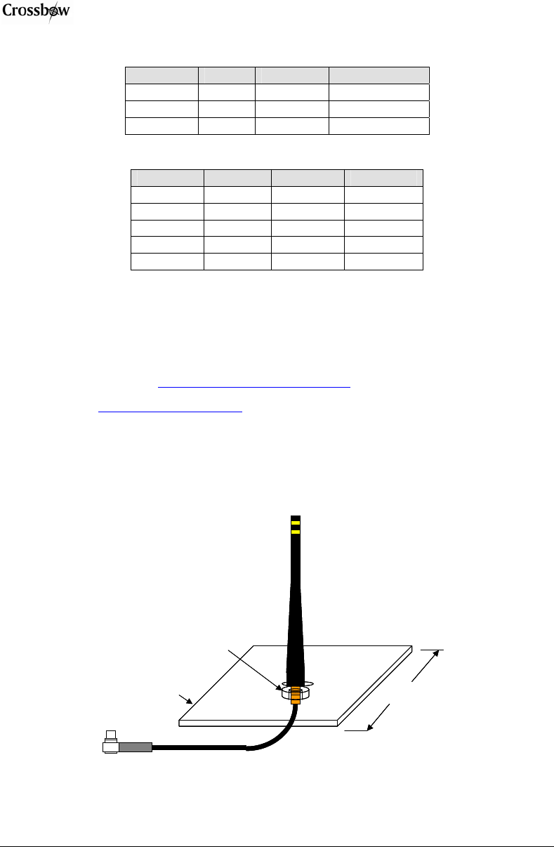
These antennas are terminated in a coax pigtail, and must have an appropriate connector
installed. They also function best with a ground plane installed, as shown in Figure 7-1. . The
ground plane can be a layer of aluminum or copper tape attached to the lid of a plastic enclosure,
or the lid of a metal enclosure.
1/2 WAVELENGTH
RECOMMENDED
METALLIC
GROUND
PLANE
NUT MAKES
CONTACT WITH
GROUND PLANE
1/2 WAVELENGTH
RECOMMENDED
1/2 WAVELENGTH
RECOMMENDED
METALLIC
GROUND
PLANE
NUT MAKES
CONTACT WITH
GROUND PLANE
Figure 7-1. Illustration of an antenna option for the motes using a Linx antenna and ground plane
Page 2 30-0549-01 Rev. B 6 Doc. # 74

IRIS OEM Edition Hardware Reference Manual
Doc. # 7430-0549-01 Rev. B Page 27
The OEM Edition module is well suited for embedded antenna designs. Proper care must be
taken in the design phase to account for packaging effects due to the enclosure, metallic parts
adjacent to the antenna, and placement on the PCB. In addition, the final application and
expected performance should be evaluated for suitable antenna choice. For an example of
embedded antenna design, Refer to the application note on “Antenna Design Considerations”.

IRIS OEM Edition Hardware Reference Manual
Page 28 Doc. # 7430-0549-01 Rev. B
8 Flash Data Logger and Serial ID Chip
All OEM Edition Modules feature a 512 k serial flash for storing data, measurements, and other
user-defined information. It is connected to one of the USART on the ATmega1281V. This chip
is supported in MoteWorks which uses this chip as micro file system. The serial flash device
supports over 100,000 measurement readings. This chip is also used for XOtap (Over the Air
Programming) services available in MoteWorks.
; NOTE: This device consumes 15 mA of current when writing data.
The OEM Edition modules also have a 64-bit serial ID chip.

IRIS OEM Edition Hardware Reference Manual
Doc. # 7430-0549-01 Rev. B Page 29
9 Atmega1281 Fuses
The ATMega1281V processor on the OEM edition modules has many programmable fuses to
control various parameters. Refer to Atmel’s technical information for the ATMega1281V for a
complete discussion of the fuses. There are two fuses that MoteWorks users should be aware of
as setting these fuses incorrectly will cause the unit to not operate correctly.
9.1 JTAG fuse
This fuse enables users to use the Atmel JTAG pod for in-circuit code debugging. Units are
shipped with JTAG enabled. As discussed in the previous section on battery voltage monitoring,
if JTAG is enabled, it will cause inaccurate measurements on ADC channel 7.
9.2 Using UISP to set fuses
The UISP utility used to download code to the OEM edition modules via a programming board
can also be used to set and unset fuses of the Atmel® ATMega1281.
Table 9-1. UISP Commands for Setting the ATMega1281’s Fuses
Action Command
Disable JTAG fuse uisp -dprog=<programmer> --wr_fuse_h=0xd9
Enable JTAG fuse uisp -dprog=<programmer> --wr_fuse_h=0x19
Enable native 128 mode uisp -dprog=<programmer> --wr_fuse_e=0xff
Use internal clock uisp -dprog=<programmer> --wr_fuse_l=0xc2
Use external clock uisp -dprog=<programmer> --wr_fuse_l=0xff
<programmer> is the device you are using to interface to the Mote from a computer. The current options
are dapa (for an MIB500), mib510 for a MIB510; and EPRB for a MIB600.
Users can also edit the file called profile in the cygwin/etc/ directory and enter an alias. One
example is this alias to disable the JTAG fuse:
alias fuse_dis="uisp -dprog=<programmer> --wr_fuse_h=0xd9"
Therefore, when fuse_dis and is entered into a Cygwin command line, the script will be
executed.
IRIS OEM Edition Hardware Reference Manual
10 Sensor Boards & Expansion Connectors
Crossbow supplies a variety of sensor and data acquisition boards for the Motes. This Chapter
describes the connectors and the functions of the pins for the MICA family sensor boards.
10.1 Sensor Board Compatibility via Expansion Connector
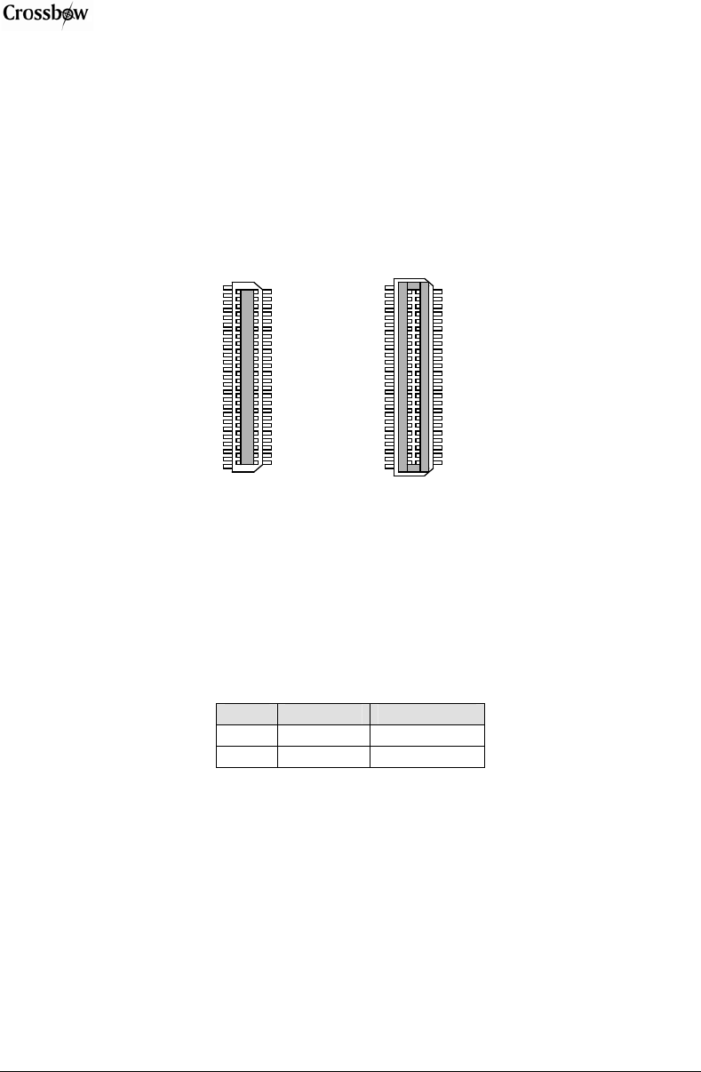
Connection to the MICA family sensor boards is made by a 51-pin connector (see Figure 10-1
below).
Page 30 Doc. # 7430-0549-01 Rev. B
27
1
1 51 26 27
51 26
Figure 10-1.The 51-pin connector used on the MICA family sensor boards;
(Left: Female; Right: Male)
The expansion connector provides a user interface for sensor boards and base stations. The
connector includes interfaces for power and ground, power control of peripheral sensors, ADC
inputs for reading sensor outputs, UART interfaces, and I2C interface, general-purpose digital
IO, and others. The part numbers of the expansion connectors are shown in Table 10-1. These
can be purchased from Digi-Key.
Table 10-1. 51-pin expansion connectors
Type Digi-Key PN Hirose PN
Female H2175-ND DF-51P-1V(54)
Male H2163-ND DF9-51S-1V(54)
IRIS OEM Edition Hardware Reference Manual
11 USB Programming Pod
The MIB520 based programming pod provides USB connectivity to the OEM Edition modules
for communication and in-system programming. It supplies power to the devices through USB
bus of the PC.
Figure 11-1. Picture of Programming Pod
11.1 ISP
The MIB520 programming pod has an on-board in-system processor (ISP) to program the Motes.
Code is downloaded to the ISP through the USB port. Next the ISP programs the code into the
Mote.
11.2 Mote Programming Using the MIB520
Programming the Motes requires having MoteWorks environment installed in your host PC. The
OEM Edition modules connect to the MIB520 via the 10-pin adapter that connects to USB port
of the host PC.
11.3 MIB520 USB Drivers
MIB520 uses FTDI FT2232C to use USB port as virtual COM port. Hence you need to install
FT2232C VCP drivers. These drivers are available in the MoteWorks CD and instructions are
provided in Section 2.1.2.
11.4 Power
The MIB520 is powered by the USB bus of the host.
11.5 USB Interface
The MIB520 offers two separate ports: one dedicated to in-system Mote programming and a
second for data communication over USB.
Doc. # 7430-0549-01 Rev. B Page 31
IRIS OEM Edition Hardware Reference Manual
Table 11-1. Pin outs for USB Connection
Pin No. Name Description
1 VBUS Powered Supply Pin
2 USBDM USB Data Signal Minus
3 USBDP USB Data Signal Plus
4 GND Ground Supply Pin
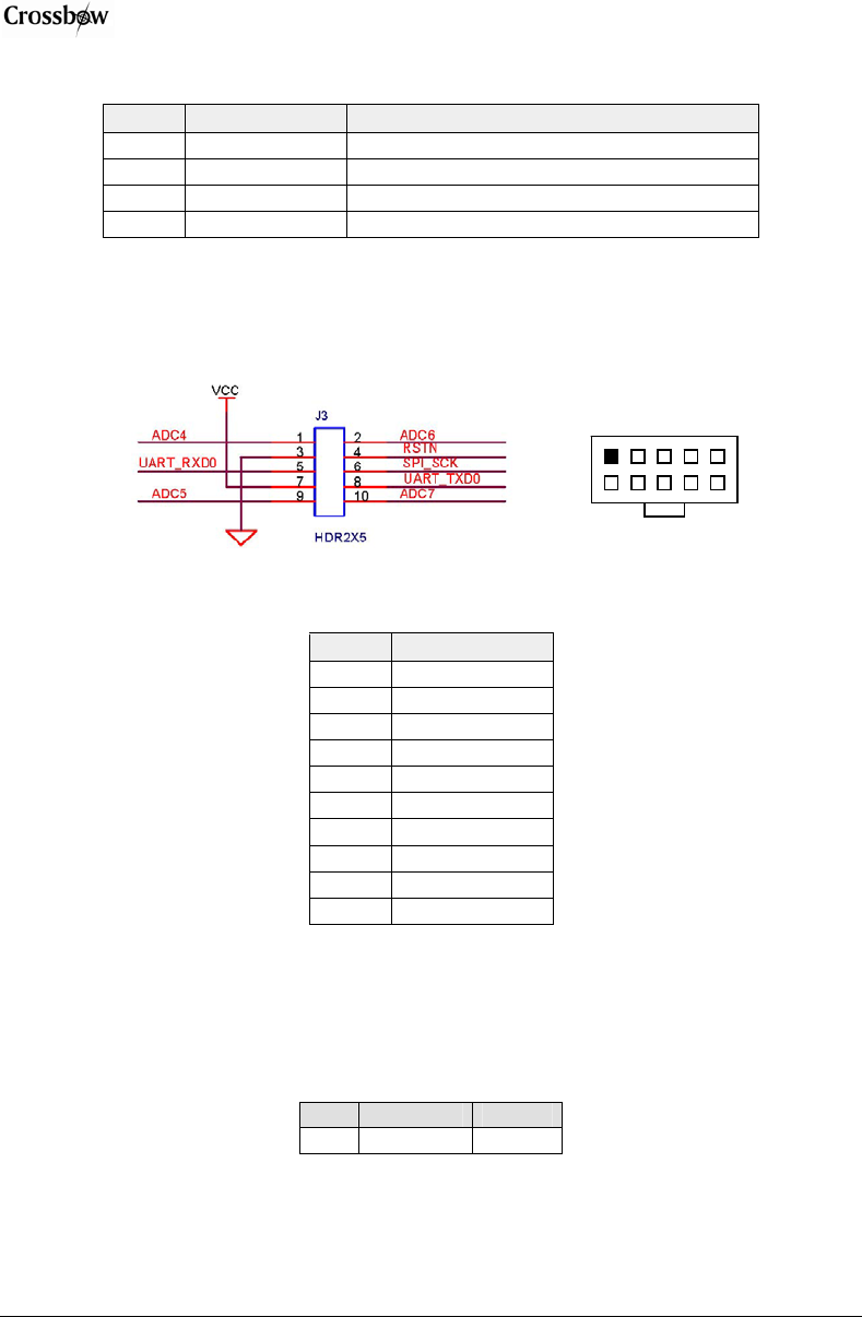
11.6 Programming Interface
The programming interface provided by MIB520 debug pod is via 10-pin connector. The pin-out
details for this connector are provided in Table 11-2.
19
210
19
210
Table 11-2. Pin outs for programming connector
Pin No. Name
1 ADC4
2 ADC6
3 GND
4 RSTN
5 UART_RXD0
6 SPI_SCK
7 VCC
8 UART_TXD0
9 ADC5
10 ADC7
When OEM customers layout their boards, it is a good idea to provide this 10-pin mating
interface to facilitate the programming of OEM edition modules. The part numbers for the
mating header/receptacle are shown in Table 11-3. These can be purchased from Digi-Key.
Table 11-3. 10-pin mating header/receptacle
Type Digi-Key PN AMP PN
Male A26267-ND 103308-1
The MIB520 debug pod is also provided with 10-pin to 51-pin adapter to facilitate the
connectivity to Crossbow’s MICA family processor/radio and sensor boards.
Page 32 Doc. # 7430-0549-01 Rev. B

IRIS OEM Edition Hardware Reference Manual
Doc. # 7430-0549-01 Rev. B Page 33
12 Appendix A. Warranty and Support Information
12.1 Customer Service
As a Crossbow Technology customer you have access to product support services, which
include:
• Single-point return service
• Web-based support service
• Same day troubleshooting assistance
• Worldwide Crossbow representation
• Onsite and factory training available
• Preventative maintenance and repair programs
• Installation assistance available
12.2 Contact Directory
United States: Phone: 1-408-965-3300 (8 AM to 5 PM PST)
Fax: 1-408-324-4840 (24 hours)
Email: techsupport@xbow.com
Non-U.S.: refer to website www.xbow.com
12.3 Return Procedure
12.3.1 Authorization
Before returning any equipment, please contact Crossbow to obtain a Returned Material
Authorization number (RMA).
Be ready to provide the following information when requesting a RMA:
• Name
• Address
• Telephone, Fax, Email
• Equipment Model Number
• Equipment Serial Number
• Installation Date
• Failure Date
• Fault Description

IRIS OEM Edition Hardware Reference Manual
Page 34 Doc. # 7430-0549-01 Rev. B
12.3.2 Identification and Protection
If the equipment is to be shipped to Crossbow for service or repair, please attach a tag TO THE
EQUIPMENT, as well as the shipping container(s), identifying the owner. Also indicate the
service or repair required, the problems encountered and other information considered valuable
to the service facility such as the list of information provided to request the RMA number.
Place the equipment in the original shipping container(s), making sure there is adequate packing
around all sides of the equipment. If the original shipping containers were discarded, use heavy
boxes with adequate padding and protection.
12.3.3 Sealing the Container
Seal the shipping container(s) with heavy tape or metal bands strong enough to handle the weight
of the equipment and the container.
12.3.4 Marking
Please write the words, “FRAGILE, DELICATE INSTRUMENT” in several places on the
outside of the shipping container(s). In all correspondence, please refer to the equipment by the
model number, the serial number, and the RMA number.
12.3.5 Return Shipping Address
Use the following address for all returned products:
Crossbow Technology, Inc.
4145 N. First Street
San Jose, CA 95134
Attn: RMA Number (XXXXXX)
12.4 Warranty
The Crossbow product warranty is one year from date of shipment.

FCC COMPLIANCE STATEMENT:
The following statement applies to M2110 OEM module:
To ensure compliance with FCC RF exposure requirements, the antenna used for this device must
be installed to provide a separation distance of at least 20cm from all persons and must not be co-
located or operating in conjunction with any other antenna or radio transmitter. Installers and end-
users must follow the installation instructions provided in this user guide.
The device complies with part 15 of the FCC rules and RSS-210. Operation is subject to the
Formatted: Font color: Auto
following two conditions: (1) This device may not cause harmful interference, and (2) this device
must accept any interference received, including interference that may cause undesired operation.
NOTE: This equipment has been tested and found to comply with the limits for a Class B digital
device, pursuant to Part 15 of the FCC Rules. These limits are designed to provide reasonable
protection against harmful interference in a residential installation. This equipment generates, uses
and can radiate radio frequency energy and, if not installed and used in accordance with the
instructions, may cause harmful interference to radio communications. However, there is no
guarantee that interference will not occur in a particular installation. If this equipment does cause
harmful interference to radio or television reception, which can be determined by turning the
equipment off and on, the user is encouraged to try to correct the interference by one or more of the
following measures:
-- Reorient or relocate the receiving antenna.
-- Increase the separation between the equipment and receiver.
-- Connect the equipment into an outlet on a circuit different from that to which the receiver is
connected.
-- Consult the dealer or an experienced radio/TV technician for help.
CAUTION: Changes or modifications not expressly approved by the party responsible for
compliance could void the user’s authority to operate the equipment.
This device has been designed to operate with the antennas listed below: Pulse Tecnitrol company,
OMNI 2dBi antenna (Model: W1030) and Crossbow, Whip 0dBi antenna (Model: Whip). and having
a maximum gain of 2 dB. Antennas not included in this list or having a gain greater than 2 dB are
strictly prohibited for use with this device. The required antenna impedance is 50 ohms.
This Class B digital apparatus complies with Canadian ICES-003
Cet appareil numérique de la classe B est conforme à la norme NMB-003 du Canada.

Crossbow Technology, Inc.
4145 N. First Street
San Jose, CA 95134
Phone: 408.965.3300
Fax: 408.324.4840
Email: info@xbow.com