CyberOptics 003 WML-C40 User Manual WaferSense TM AGS User s Guide
CyberOptics Semiconductor WML-C40 WaferSense TM AGS User s Guide
Contents
Users Manual

CyberOptics
Semiconductor
WaferSense™
AGS User’s
Guide

ii
General
Information
WaferSense Gapping Wafer and Link
Changes or modifications not expressly approved by CyberOptics Semiconductor, Inc., may
void your authority to operate the WaferSense AGS.
The radio contained in the WaferSense AGS meets all the applicable FCC requirements for RF
Safety. While in operation, the FCC requires users and nearby persons to maintain a minimum
separation distance of 20 cm (8 inches) or farther from the WaferSense AGS.
The WaferSense Gapping Wafer and Link have been tested and found to comply with the
limits for a Class B digital device, pursuant to Part 15 of the FCC Rules. These limits are
designed to provide reasonable protection against harmful interference in a residential
installation. This equipment generates, uses and can radiate radio frequency energy and, if not
installed and used in accordance with the instructions, may cause harmful interference to radio
communications. However, there is no guarantee that interference will not occur in a particular
installation. If this equipment does cause harmful interference to radio or television reception,
which can be determined by turning the equipment off and on, the user is encouraged to try to
correct the interference by one or more of the following measures:
• Reorient or relocate the receiving antenna.
• Increase the separation between the equipment and receiver.
• Connect the equipment into an outlet on a circuit different from that to which the
receiver is connected.
• Consult the dealer or an experienced radio/TV technician for help.
This device complies with part 15 of the FCC Rules. Operation is subject to the following two conditions: (1)
This device may not cause harmful interference, and (2) this device must accept any interference received, including
interference that may cause undesired operation.
This ISM device complies with Canadian ICES-001.
Cet appareil ISM est conforme à la norme NMB-001 du Canada.
Caution
Electrostatic discharge (ESD) can damage the AGS. Handle the AGS in an ESD-safe
area. If such an area is not available, wear an antistatic wrist strap or touch a grounded
surface before handling the AGS.
iii
WaferSense Technical Support
Technical support is available from CyberOptics Semiconductor Monday through Friday,
8:00 A.M. to 5:00 P.M. Pacific Time.
WaferSense and GapView are trademarks of CyberOptics Semiconductor, Inc.
Third-party brands and names are the property of their respective owners.
Copyright © 2006-2008, CyberOptics Semiconductor, Inc. All rights reserved.
CyberOptics Semiconductor, Inc.
13555 S.W. Millikan Way
Beaverton, OR 97005
P/N 920-0701-02
E-mail: CSsupport@cyberoptics.com
Phone: +1 503 495-2200
800-366-9131 (US and Canada only)
Fax: +1 503 495-2201

iv
Table of
Contents
General Information ......................................................ii
Chapter 1
Introduction....................................................................................1.1
Chapter 2
Installing Your AGS....................................................................... 2.1
Installing the Software....................................................................2.1
Installing the Wireless Link............................................................2.3
Checking Communications Between the Link and the Wafer ......2.5
Registering Your Gapping Wafer for Calibration Service..............2.6
Running the GapView Application ................................................2.7
Technical Support ..........................................................................2.9
Chapter 3
Using Your AGS............................................................................. 3.1
Opening and Closing the Clean Box..............................................3.2
Using the AGS Gapping Wafer Buttons and Status Lights ...........3.3
Performing a Basic Gap Measurement ..........................................3.4
Setting the Gap Criteria ..................................................................3.9
Applying Offsets to the Gap Readings......................................... 3.10
Setting the Wafer Display Orientation .........................................3.12
Logging Your Readings ...............................................................3.13
Logging a Reading..................................................................................3.13
Including User-Specified Information in the Log File .....................3.14
Changing the Log File............................................................................3.15
Displaying Readings from a Log File ..................................................3.15
Printing the GapView Window.....................................................3.16
Monitoring the Operating Temperature ...................................... 3.17
Table of Contents
v
Using the Rechargeable Battery................................................... 3.18
Monitoring the Battery Level................................................................3.18
Charging the Battery ..............................................................................3.18
Monitoring the Wireless Connection to the Gapping Wafer ....... 3.19
Changing the Pairing Between the Gapping Wafer and Link .....3.20
Saving Your Settings..................................................................... 3.21
Loading Settings from a File.................................................................3.21
Chapter 4
Maintaining Your AGS .................................................................. 4.1
Annual Factory Calibration and Battery Replacement ..................4.2
Battery Use and Disposal ...............................................................4.2
Field Calibrating Your AGS............................................................4.3
Chapter 5
Specifications................................................................................. 5.1
System Requirements .....................................................................5.1
AGS Hardware ................................................................................5.1
Environmental ..........................................................................................5.1
Power..........................................................................................................5.1
Range and Accuracy.................................................................................5.1
Index.....................................................................Index.1

vi
List of
Illustrations
Chapter 2
Figure 2.1: The InstallShield Wizard.......................................................2.2
Figure 2.2: Found New Hardware Wizard..............................................2.3
Figure 2.3: Installing the Wireless Link Device......................................2.4
Figure 2.4: Starting the GapView Application ........................................2.7
Figure 2.5: Calibration Registration Dialog............................................2.8
Figure 2.6: The About GapView Dialog..................................................2.9
Figure 2.7: The About your AGS Wafer Dialog ......................................2.9
Chapter 3
Figure 3.1: Opening the Clean Box.........................................................3.2
Figure 3.2: Gap Measurements ...............................................................3.4
Figure 3.3: The GapView Application.....................................................3.5
Figure 3.4: Aligning the Gapping Wafer .................................................3.6
Figure 3.5: Numeric Readouts................................................................3.7
Figure 3.6: Graphical Readouts...............................................................3.8
Figure 3.7: Set Gap Criteria Dialog .........................................................3.9
Figure 3.8: Set Gap Offsets Dialog........................................................ 3.10
Figure 3.9: Applying the Gap Offset ..................................................... 3.11
Figure 3.10: Wafer Orientation in GapView..........................................3.12
Figure 3.11: Logging a Reading ............................................................ 3.14
Figure 3.12: Set Station Information dialog .......................................... 3.15
Figure 3.13: Temperature Monitoring Gauge ....................................... 3.17
Figure 3.14: Battery Monitor ................................................................. 3.18
Figure 3.15: Wireless Connection Monitor............................................3.20
Chapter 4
Figure 4.1: Wafer Calibration Status Dialog............................................4.2
Figure 4.2: Field Calibrate Button and Last Calibration ........................4.3
Figure 4.3: Step 1 of 3 Start Calibration Dialog.......................................4.4
Figure 4.4: Step 2 of 3 Place AGS Wafer Dialog......................................4.4
Figure 4.5: Step 3 of 3 Finish Calibration Dialog....................................4.5

1.1
Chapter 1
Introduction
The CyberOptics Semiconductor WaferSense™ Automatic Gapping System (AGS) measures
gaps that are critical to the outcome of semiconductor processes such as thin-film deposition,
sputtering, and etch. It uses a capacitive sensing technique (patent pending) that consists of
three sensors and responds to the proximity of a conductive electrode, such as a shower head,
to return live gap measurements that display on your laptop or PC in numerical and graphical
form. The GapView™ software application makes it easy to precisely adjust equipment. The
large display and wireless link let you place the computer at a convenient distance from the
AGS gapping wafer.
AGS consists of the following components:
•Gapping wafer. The gapping wafer is designed with a wafer-like form factor, so it
can fit in most wafer-handling equipment. The gapping wafer package is also vacuum
compatible.
•GapView software. The GapView software application monitors the gapping wafer
and displays gap measurements and other status information in real time. GapView
runs on most personal computers that use the Microsoft Windows operating system.
•Wireless link. The GapView software communicates with the gapping wafer by
using a Bluetooth wireless link that attaches to a USB port on a personal computer.
•Clean box. The clean box lets you store the wafer when not in use.
•Battery charger and adapter cable. The battery charger and adapter cable let you
recharge the gapping wafer’s battery.
•Carrying case. The carrying case makes it easy to take your complete AGS system
with you in the plant or on the road.
The following chapter gives you instructions for installing your AGS system.
2.1
Chapter 2
Installing Your AGS
This chapter describes the procedures you need to perform to install your AGS and get it ready
for use. For best results, perform the procedures in the order they are presented in this chapter:
1. Installing the software
2. Installing the wireless link on the USB port
3. Checking communications between the link and the gapping wafer
4. Registering your gapping wafer
5. Running the GapView application
Installing the Software
To run the WaferSense AGS software, your computer must have the following:
• Windows 2000, Windows XP, or Windows Vista operating system
• One free high-power USB 1.1 or USB 2.0 port
To install the WaferSense AGS software:
1. Log on using an account with Administrator privileges.
Caution
Dropping the gapping wafer or hitting it against a hard object can bend, break, or chip the
housing; damage the internal components; or knock the gapping wafer out of calibration.
While it is not as fragile as an actual silicon wafer, handle the gapping wafer with care, as
you would any precision instrument. If the gapping wafer is damaged or in need of
calibration, see Chapter 4, “Maintaining Your AGS.”
Chapter 2. Installing Your AGS
2.2
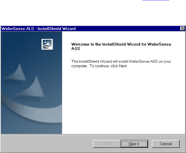
2. Insert the WaferSense AGS Installation Disk into the CD drive.
The InstallShield Wizard starts automatically, as shown in Figure 2.1. If the wizard doesn’t
start automatically, use Windows Explorer to view the contents of the CD and double-
click the setup.exe program.
Figure 2.1: The InstallShield Wizard
3. Follow the instructions provided by the wizard to install the software.
4. After you complete the instructions for all of the wizard screens, click Finish. If
Windows notifies you that the drivers have not passed Windows logo testing, just click
Continue Anyway to complete the installation.
By default, the Setup program installs the GapView application in a new program group called
WaferSense AGS. Setup also installs an online copy of this user’s guide, which is available from
the GapView Help menu and in the WaferSense AGS program group in the Windows
Start menu.
Chapter 2. Installing Your AGS
2.3
Installing the Wireless Link
To install the wireless link:
1. Turn on your computer.
2. Locate an unused, high-power USB port on your computer. The AGS wireless link
module requires a high-power USB port, such as the built-in ports on your computer and
ports on USB hubs that have power cords. Unpowered USB hubs won’t work.
3. The USB cable provided with your AGS has a different plug on each end. Locate the end
with the plug that matches the USB port on your computer and plug the cable into
the port.
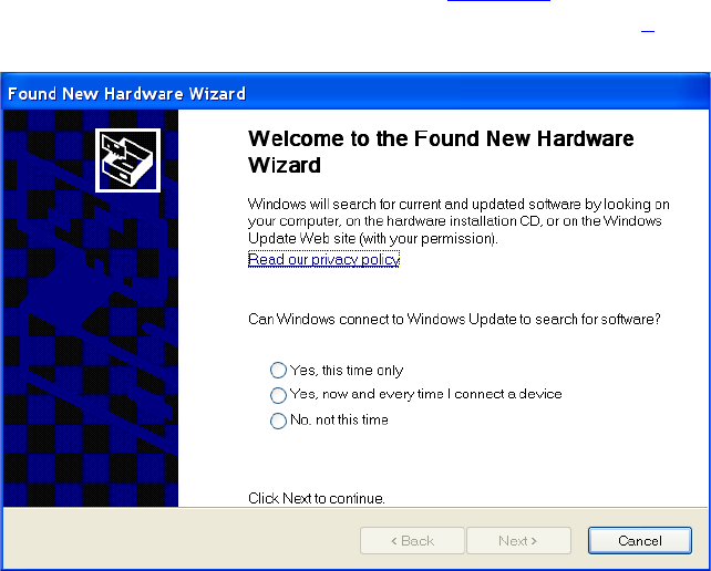
4. Plug the other end of the cable into the link module.
The Windows operating system recognizes the new link module hardware and displays
the Found New Hardware Wizard, as shown in Figure 2.2. If the wizard your system
displays doesn’t offer to check with Windows Update, skip to step 6.
Figure 2.2: Found New Hardware Wizard
5. Choose No, not this time and click Next.
Chapter 2. Installing Your AGS
2.4
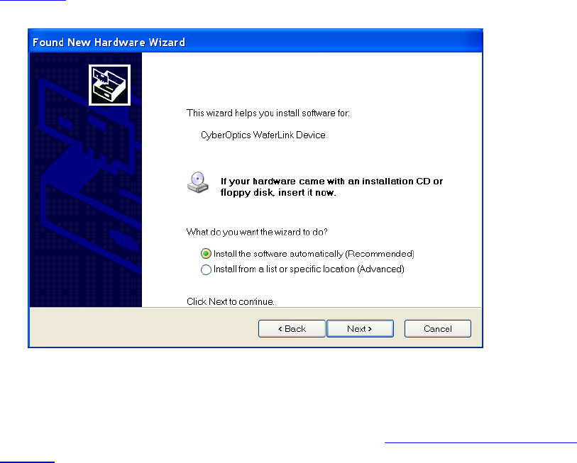
The wizard offers to help you install software for the WaferSense link, as shown in
Figure 2.3.
Figure 2.3: Installing the Wireless Link Device
6. Choose Install the software automatically and click Next.
If you already installed the WaferSense AGS software (see “Installing the Software,” on
page 2.1), Windows will automatically find the drivers. If not, the drivers are located in the
Utilities folder on the installation CD-ROM.
7. After you complete the instructions for all of the wizard screens, click Finish.
The Power light on the module turns on indicating that the module is getting power from
the USB port. Ignore the Pair Status and Connection Status lights for now.
Chapter 2. Installing Your AGS
2.5
Checking Communications Between the Link
and the Wafer
To complete the installation, verify that the gapping wafer and link can communicate as
follows:
1. The gapping wafer operates from an internal rechargeable battery. Before using the
gapping wafer for the first time, charge it for two hours. For information on checking the
charge on the battery and the procedure for recharging, see “Using the Rechargeable
Battery,” on page 3.18.
2. Unplug the battery charger, open the clean box (see “Opening and Closing the Clean
Box,” on page 3.2), and remove the wafer from the box.
3. Press the ON / OFF button to turn on the gapping wafer.
The Power light on the gapping wafer turns on.
4. Verify that the Pair Status lights on both the gapping wafer and link module are on. If
either light is not on, your gapping wafer and link might not be paired with each other. To
reset the pairing, see “Changing the Pairing Between the Gapping Wafer and Link,” on
page 3.20.
5. Immediately after turning on the gapping wafer, the Connection Status lights on the
gapping wafer and link will blink slowly. After a few seconds the gapping wafer and link
will connect and both lights will be on and no longer blinking. If the lights continue to
blink, see “Monitoring the Wireless Connection to the Gapping Wafer,” on page 3.19.
6. After starting the GapView application (see “Running the GapView Application,” on
page 2.7), you can verify the connection to the gapping wafer by comparing the serial
number printed on the gapping wafer to the serial number shown in the About your AGS
Wafer dialog, which is available in the GapView application by choosing the Help >
About your AGS Wafer menu item. If the GapView application isn’t running, the AGS
wafer turns off automatically after 30 minutes.
That completes the installation of your AGS.

Chapter 2. Installing Your AGS
2.6
Registering Your Gapping Wafer for Calibration
Service
To maintain optimum performance, every twelve months you should have your gapping wafer
calibrated and the battery replaced. These services can be performed only at the factory.
To help you keep track of the next service date so you can schedule this service when it is
convenient, register your WaferSense AGS gapping wafer with the factory. When you start the
GapView application (see “Running the GapView Application,” on page 2.7), it prompts you to
register your gapping wafer for calibration. You can also register your gapping wafer in any of
the following ways:
• On the Internet: http://www.cyberopticssemi.com/ws_register.html
• By phone: 800-366-9131 (US and Canada only)
• By faxing the WaferSense AGS Calibration Registration to: +1 503 495-2201
• By sending an e-mail message containing the information specified on the WaferSense
AGS Calibration Registration to: register@cyberoptics.com.
Chapter 2. Installing Your AGS
2.7
Running the GapView Application
To start the GapView application:
1. From the Windows Start > All Programs menu, choose WaferSense AGS > GapView.
The GapView application starts, as shown in Figure 2.4. Initializing communications
between the gaping wafer and GapView usually takes less than one second. For
information on using GapView, see “Chapter 3, Using Your AGS.” If you haven’t
registered your gapping wafer, GapView also displays the Calibration Registration dialog.
To complete the registration, proceed to the next step.
Figure 2.4: Starting the GapView Application
Chapter 2. Installing Your AGS
2.9
Technical Support
CyberOptics Semiconductor offers free technical support to customers. If the AGS hardware
or the GapView software appear to be malfunctioning, please contact us, and we’ll be happy to
assist you.
When you contact us, please make sure that you have the following information available:
• A detailed description of the problem you are having, including the exact text of any
error messages and a list of steps to reproduce the problem.
• Information about your computer, including manufacturer, CPU type, version of
Windows, and memory size.
• The version of the GapView application. The software version is available in the
GapView application by choosing the Help > About GapView menu item.
Figure 2.6: The About GapView Dialog
• The serial number of your gapping wafer. The serial number of the gapping wafer is
printed on a label on the side of the gapping wafer. The serial number is also available
in the GapView application by choosing the Help > About your AGS Wafer menu
item.
Figure 2.7: The About your AGS Wafer Dialog
Technical support is available Monday through Friday, 8:00 A.M. to 5:00 P.M. Pacific Time.
• Voice: +1 503 495-2200

3.1
Chapter 3
Using Your AGS
This chapter gives you instructions for performing the following tasks with the AGS:
• Opening and closing the clean box
• Using the AGS gapping wafer buttons and indicators
• Performing a basic gap measurement
• Setting the gap criteria for measurements
• Applying offsets to the gap measurements
• Setting the wafer display orientation
• Logging your readings
• Printing the GapView window
• Monitoring the operating temperature
• Using the rechargeable battery
• Monitoring the connection between the gapping wafer and link module
• Changing the pairing between the gapping wafer and link module.
• Saving your settings
Chapter 3. Using Your AGS
3.2
Opening and Closing the Clean Box
The gapping wafer comes in a plastic clean box that is used for the storing wafer when not in
use and for charging the rechargeable battery in the wafer (see “Using the Rechargeable
Battery,” on page 3.18).
To open the case:
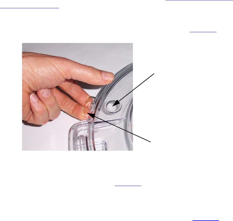
1. Place your thumbs in the raised circles on the top of the case (see Figure 3.1).
Figure 3.1: Opening the Clean Box
2. Using your fingertips under the tabs, lift up on the lid of the clean box while you press
down with your thumbs, as shown in Figure 3.1.
To close the clean box:
1. Lower the lid.
2. Place both thumbs on the raised circles on the top of the case (see Figure 3.1) and press
down until the case snaps shut.
Press your thumbs
in the circles
Pull up on the
tabs with your
fingertips

Chapter 3. Using Your AGS
3.3
Using the AGS Gapping Wafer Buttons and
Status Lights
AGS gapping wafers have two buttons:
•ON / OFF. Turns the gapping wafer on and off. If the GapView application isn’t
running, the AGS wafer turns off automatically after 30 minutes.
•PAIR. Changes the pairing between a gapping wafer and a link (see “Changing the
Pairing Between the Gapping Wafer and Link,” on page 3.20).
AGS gapping wafers also have the following status lights:
•Power. On while the gapping wafer is turned on.
•Charging. On when the gapping wafer is being charged.
•Charging Done. On when the battery has reached at least 90% of full charge.
•Pair Status. On when the gapping wafer is paired with a link (see “Changing the
Pairing Between the Gapping Wafer and Link,” on page 3.20).
•Connection Status. On when the gapping wafer has established communication
with the link. Blinks slowly while the gapping wafer is trying to establish a connection
with the link.
Chapter 3. Using Your AGS
3.4
Performing a Basic Gap Measurement
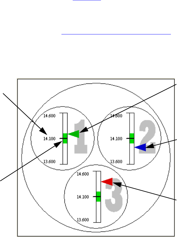
The AGS gapping wafer uses three sensors that respond to the proximity of a conductive
surface, such as a shower head. Using these sensors, AGS measures the gap, the distance
between the bottom of the gapping wafer and the surface of the equipment above the gapping
wafer, at three points (see Figure 3.2). You can use these three gap measurements to adjust the
equipment so that the gapping wafer and the shower head or other surface are parallel, to
within your specified tolerance.
Figure 3.2: Gap Measurements
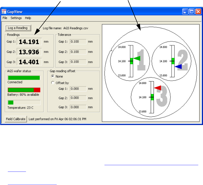
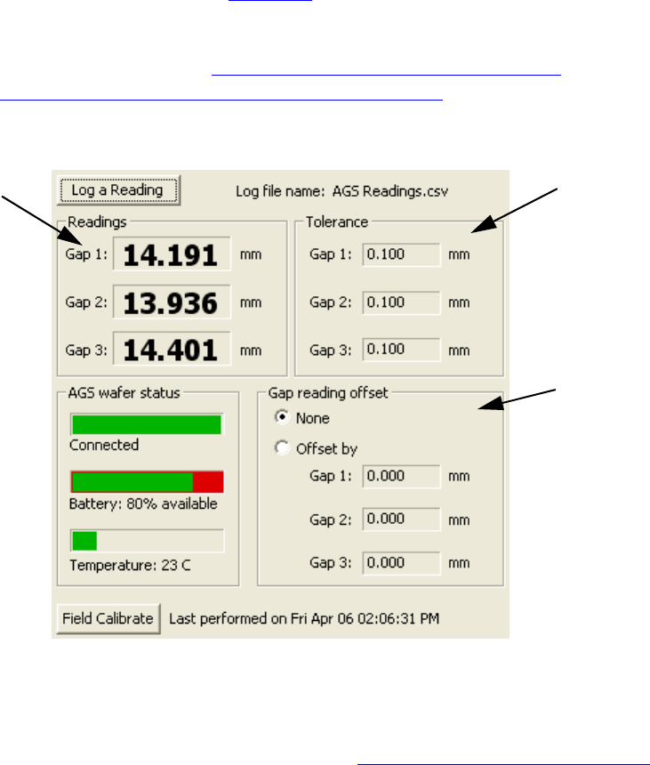
GapView shows these gap measurements using two types of readouts (see Figure 3.3):
• Graphical readouts
• Numeric readouts
12
3
Shower head
Gapping
Wafer
Chapter 3. Using Your AGS
3.5
GapView updates the readings about once per second, so you see any changes in real time.
Figure 3.3: The GapView Application
To perform a basic gap measurement:
1. Place the gapping wafer on the equipment you want to check (for instructions on
removing the wafer from the clean box, see “Opening and Closing the Clean Box,” on
page 3.2). Align the gapping wafer so it matches the GapView display by rotating the
gapping wafer until the numbers on the gapping wafer pads are aligned as shown in
Figure 3.4 on page 3.6.
Numeric Readouts Graphical Readouts
Numeric Readouts Graphical Readouts
Chapter 3. Using Your AGS
3.6
Figure 3.4: Aligning the Gapping Wafer
The gapping wafer also has a notch on one side. When you have the gapping wafer
aligned as described above, the notch will be in the 10 o’clock position as you face the
gapping wafer.
You can change the orientation of the gapping wafer in the GapView display. For
example, if you have equipment where the wafer must be oriented with the notch in the
6 o’clock position, you could set GapView to display the wafer in that position (see
“Setting the Wafer Display Orientation,” on page 3.12).
Notch
2
3
1
2
3
1
Chapter 3. Using Your AGS
3.7
2. Make sure the computer running the GapView application is within the range of the
gapping wafer, about 30 ft (10 m).
3. The numeric readouts and graphic readouts indicate the three gap measurements:
•The numeric readouts (see Figure 3.5) indicate the gap measurements, to 0.0001 inch
or 0.001 mm, in real time. Readings outside the working range of the gapping wafer
are displayed in gray rather than black. GapView also displays the current settings for
the target gap tolerances (see “Setting the Gap Criteria” on page 3.9.) and offsets (see
“Applying Offsets to the Gap Readings,” on page 3.10). You can change units (mm or
inch) when you set gap criteria or offsets.
Figure 3.5: Numeric Readouts
The numeric readouts don’t change size if you change the size of the GapView window.
For information on the accuracy of the readings, see “Range and Accuracy,” on page 5.1.
Numeric
readouts
Tolerances
Offsets
Chapter 3. Using Your AGS
3.8
• The graphical readouts (see Figure 3.6) show the gap measurements in real time. Each
circle (1, 2, and 3) shows a ruler, marked with the target gap distance in the middle of
the ruler. The green band in the middle of the ruler corresponds to the tolerance for
the gap measurement. You can set the target gap distance and tolerance for the three
gap measurements (see “Setting the Gap Criteria,” on page 3.9).
An arrowhead next to each ruler points to the current gap measurement. The color of
the arrowhead indicates whether the current gap measurement is within tolerance
(green), too small (blue), or too big (red).
Figure 3.6: Graphical Readouts
You can make the graphical display larger or smaller by changing the size of the
GapView window. Other controls in the window do not change size.
Target gap
Red
arrowhead
means gap
is too big.
Green
arrowhead
means gap
is within
tolerance.
Tolerance
band
Blue
arrowhead
means gap
is too small.
Chapter 3. Using Your AGS
3.9
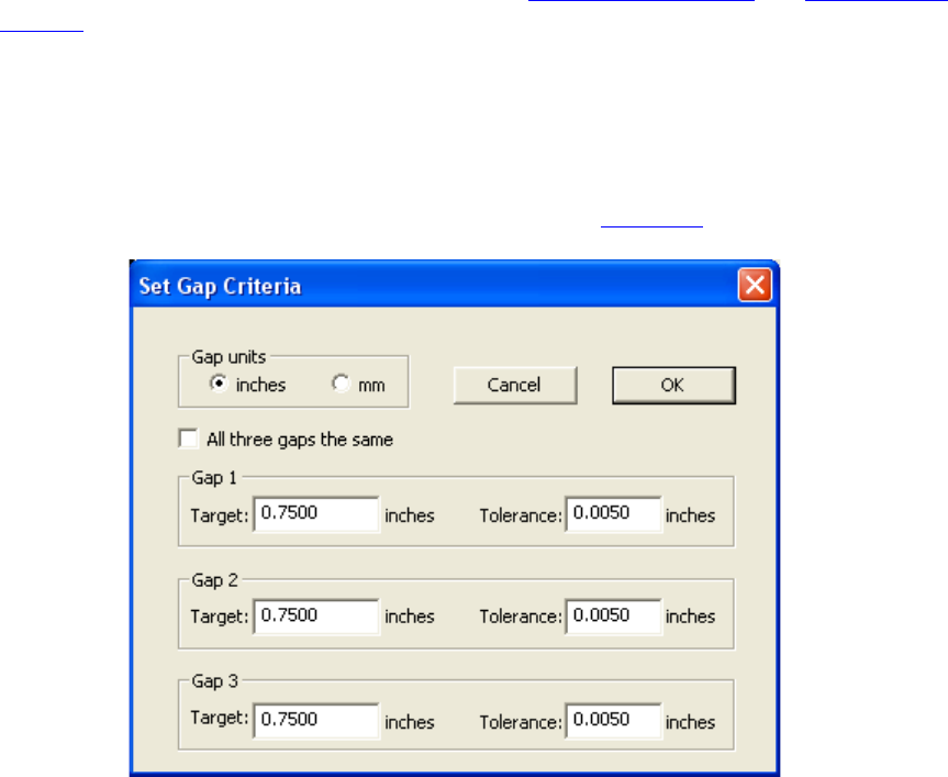
Setting the Gap Criteria
You can set the target gap distance and the tolerance for the gap measurement, which are
indicated in the numeric and graphical displays (see Figure 3.5 on page 3.7 and Figure 3.6 on
page 3.8). You can set individual values for each of the three gaps, or you can specify one target
and tolerance value for all three measurements. You can also specify whether you want
GapView to use units of inches or millimeters for gap measurements.
To specify the gap criteria:
1. Choose the menu item Settings > Set Gap Criteria.
The Set Gap Criteria dialog is displayed, as shown in Figure 3.7.
Figure 3.7: Set Gap Criteria Dialog
2. In the Gap Units section, choose the units of measurement, inches or millimeters. This
selection affects all values in the dialog and in the main GapView window.
3. To specify the same target gap distance and tolerance for all three gap measurements,
check the box for All three gaps the same. To specify the target gap distance and
tolerance separately for each of the three measurements, uncheck the box. When you
check the box, the dialog changes to display only one set of gap criteria.
4. For the displayed gaps (All gaps or Gap 1, Gap 2, and Gap 3), fill in the target gap
distance and the tolerance.
5. Click OK.
Chapter 3. Using Your AGS
3.10
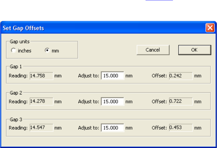
Applying Offsets to the Gap Readings
By default, GapView displays the actual measurements from the gapping wafer’s sensors. If you
use other instruments to measure or set gaps, the measurements of those instruments might not
agree with those of the AGS because of differences in technology or calibration. If you want
the AGS readings to agree, you can use the offsets feature of GapView to add an adjustment to
the displayed measurements. You do this by having the AGS measure the gap and then telling
GapView what you want the displayed readings to be. GapView calculates the difference
between the actual AGS measurements and your specified values and applies these offsets to
the displayed readings.
To apply an offset to the gap readings displayed in GapView:
1. Choose the menu item Settings > Set Gap Offsets.
The Set Gap Offsets dialog is displayed, as shown in Figure 3.7. The current gap readings
are shown in the Reading box for each gap.
Figure 3.8: Set Gap Offsets Dialog
2. In the Gap Units section, choose the units of measurement, inches or millimeters. This
selection affects all values in the dialog and in the main GapView window.
3. In the Adjust to box for each gap, fill in the value you want GapView to display for the
current gap being measured. GapView calculates the difference between the adjusted
setting and the current reading and displays this offset.
4. After setting all gap offsets, click OK.
Chapter 3. Using Your AGS
3.11
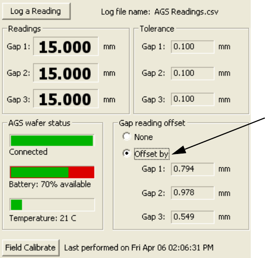
5. In the GapView main window, in the Gap reading offset controls, choose Offset by to
apply the offsets.
Figure 3.9: Applying the Gap Offset
To stop GapView from applying the gap offsets, in the Gap reading offset controls,
choose None.
Choose Offset
by to apply the
offsets
Chapter 3. Using Your AGS
3.12
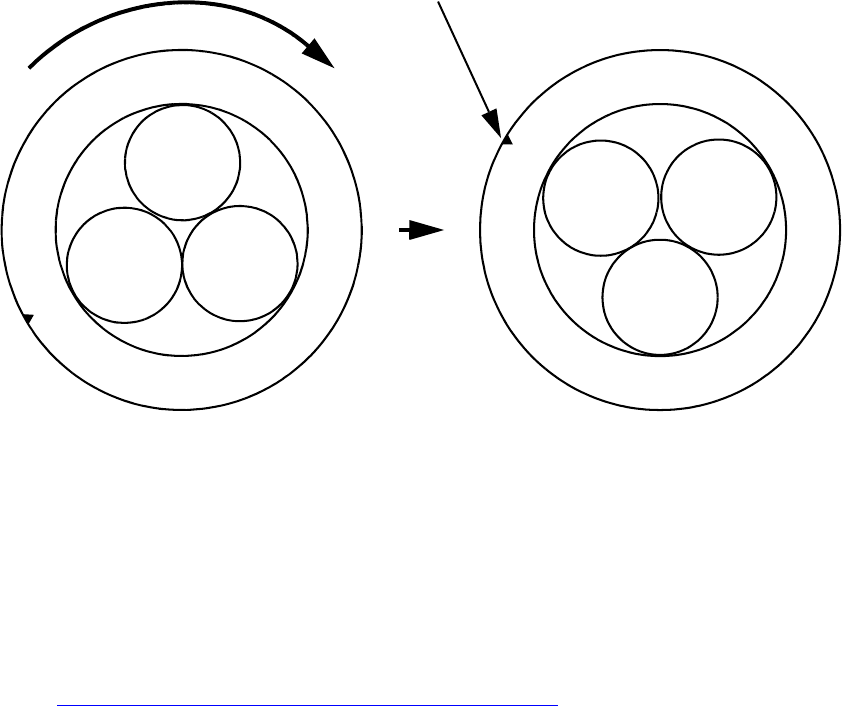
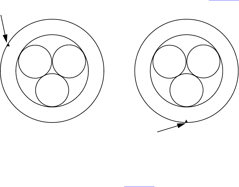
Setting the Wafer Display Orientation
Checking and adjusting equipment is easier if you can place the gapping wafer in the equipment
in the same orientation as it is shown in the GapView display. By default, the wafer is displayed
in GapView with the notch in the 10 0’clock position, as shown on the left in Figure 3.10.
Figure 3.10: Wafer Orientation in GapView
If you have a piece of equipment that requires the wafer to be in a different orientation, you can
tell GapView to rotate the displayed wafer to any of six positions: 2, 4, 6, 8, 10, or 12 o’clock.
For example, the wafer display on the right in Figure 3.10 is shown with the notch at the
6 o’clock position. The sensor pads have also rotated so that pad 1 is now at the bottom.
To change the orientation of the wafer in the GapView display:
• Choose the desired orientation from the menu item Settings > Set Display
Orientation. > Notch at X o’clock.
Notch
2
3
123
1
Notch
Chapter 3. Using Your AGS
3.13
Logging Your Readings
GapView can keep a record of your activities as you use the gapping wafer to check the gap of
various pieces of equipment. GapView keeps the record in a log file. You can specify the log file
path (see “Changing the Log File,” on page 3.15). The log file contains the following
information for each entry:
•Date and Time. The date and time of the log file entry.
•Gap units. Measurement units for gap measurements: inches or millimeters (see
“Setting the Gap Criteria,” on page 3.9).
•Gap and In Range. Measurements for Gap 1, Gap 2, and Gap 3. Following the
three measurements, the next three entries indicate whether the corresponding gap
measurements were within tolerance (“good”), too big (“too high”), or too small
(“too low”).
•Target and Tolerance. The user-specified target values for each gap, followed by the
user-specified tolerance for each gap measurement (see “Setting the Gap Criteria,” on
page 3.9).
•Offsets. Whether or not to apply the user-specified offsets when displaying gap
measurements followed by the three offset values (see “Applying Offsets to the Gap
Readings,” on page 3.10).
•Temperature. The current operating temperature of the gapping wafer in °C (see
“Monitoring the Operating Temperature,” on page 3.17).
•Battery. The percentage of time remaining before the battery must be recharged (see
“Using the Rechargeable Battery,” on page 3.18).
•Serial Number. The serial number of the gapping wafer.
•Operator, Tool, Station, and Comment. Text fields you can use to record your own
information with each log entry (see “Including User-Specified Information in the
Log File,” on page 3.14).
The remainder of this section tells you how to:
• Log a reading
• Include information in a log entry for operator, tool, station, and comment
• Specify a different location or file name for the log file
• Display a past reading from a log file
Logging a Reading
GapView posts entries to the log file on your command.
To post an entry to the log file:
• In the main GapView window, click Log a Reading (see Figure 3.11 on page 3.14).
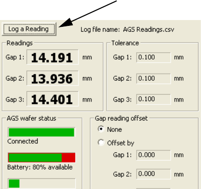
Chapter 3. Using Your AGS
3.14
GapView immediately writes a log entry each time you click the button.
Figure 3.11: Logging a Reading
Including User-Specified Information in the Log File
Operator, Tool, Station, and Comment are text fields you can use to record your own
information with each log entry. You can fill in any text information you want in these fields.
To include user-specified information for logging:
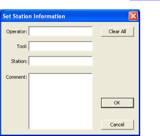
1. Choose the Settings > Set Station Information menu item.
Log a Reading button
Chapter 3. Using Your AGS
3.15
The Set Station Information dialog is displayed, as shown in Figure 3.12.
Figure 3.12: Set Station Information dialog
2. Type your text into the Operator, Tool, Station, and Comment text fields.
3. You can leave the Set Station Information dialog open while using GapView. Doing so
makes it easy to change the Comment or other fields each time you log a reading, or as
needed. If you want to close the dialog, click OK.
You can change or delete this information at any time for future log entries. To quickly clear all
of the fields, click Clear All.
Changing the Log File
By default, GapView writes log entries to the file My Documents\AGS Files\AGS
Readings.csv. If you prefer, you can specify a different log file.
To change the log file:
1. Choose the File > Select Log File menu item.
2. In the AGS Log File dialog, specify the folder and file name for the log file, and
click Save.
Displaying Readings from a Log File
Log files are saved in a comma-separated-values (CSV) text format. The file is read-only to
avoid accidental data corruption. Files in CSV text format are easy to import into spreadsheet
and word processing programs.
Chapter 3. Using Your AGS
3.16
Printing the GapView Window
You can print an image of the GapView window to have a graphical record of the session.
To print an image of the GapView window:
1. Choose File > Print.
2. In the Print dialog, click OK.
You can also select a printer other than the default and change the printer setup, or see a
preview of what GapView will print:
• To select a different printer, change the paper selection or print orientation, or set
printer properties, choose the File > Print Setup menu item.
• To see a preview of what GapView will print, choose the File > Print Preview menu
item.
Chapter 3. Using Your AGS
3.17
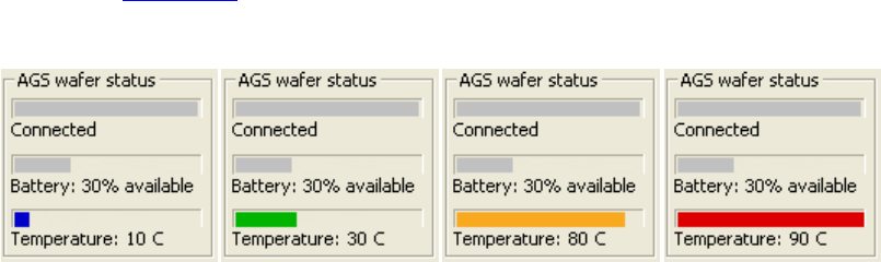
Monitoring the Operating Temperature
The operating range for the gapping wafer to achieve the specified accuracy for gap readings is
20 °C - 70 °C. The Temperature monitor in the AGS wafer status area of the GapView
window (see Figure 3.13) shows the current operating temperature of the gapping wafer with a
numeric readout and a bar graphic.
Figure 3.13: Temperature Monitoring Gauge
The thermometer indicates the upper and lower limits of the operating temperature range. The
bar changes color as an additional indication of where the current temperature is relative to the
accurate operating range:
•Blue. Less than 20 °C; the gapping wafer is operating below the range where it
produces accurate readings.
•Green. 20 °C to 70 °C; the gapping wafer is operating in its normal temperature
range, where it produces readings meeting the specified accuracy.
•Orange. Greater than 70 °C to 80 °C; the gapping wafer is operating above the range
where it produces the most accurate readings, but not so hot that the gapping wafer
will be damaged.
•Red. Greater than 80 °C; the gapping wafer is operating at a temperature so high that
it might be damaged.
High
>70-80 °C Too High
>80 °C
Low
< 20 °C OK
20-70 °C
Chapter 3. Using Your AGS
3.18
Using the Rechargeable Battery
The gapping wafer operates from an internal rechargeable battery. From a full charge, the
battery provides about 4 hours of continuous use. Before using your gapping wafer for the first
time, charge it for two hours.
The battery can be recharged about 500 times before the charge life starts to degrade
significantly. The battery is not user replaceable. For information on replacing the battery, see
“Annual Factory Calibration and Battery Replacement,” on page 4.2.
Monitoring the Battery Level
GapView receives frequent updates from the gapping wafer on the state of the gapping wafer’s
battery. The Battery indicator in the AGS wafer status area of the GapView window shows
the approximate percentage of operating time remaining before you must charge the battery.
Figure 3.14: Battery Monitor
Charging the Battery
You can charge the gapping wafer while it is in the clean box or outside the clean box. To
charge the gapping wafer’s battery:
1. Use only the battery charger supplied with your gapping wafer. Using a different battery
charger might damage your gapping wafer or create a safety hazard.
2. Do not charge the gapping wafer if its internal temperature is higher than 45 °C. Charging
the gapping wafer at a temperature higher than 45 °C might damage your gapping wafer
or create a safety hazard.
3. Plug the charger adapter cable into the socket labeled CHARGER in the gapping wafer.
4. If you want to place the gapping wafer into the clean box, leave the lid open or close it
loosely. The adapter cable or clean box can be damaged if you close the lid tightly while
charging the gapping wafer. (For instructions on how to open and close the clean box, see
“Opening and Closing the Clean Box,” on page 3.2.)

Chapter 3. Using Your AGS
3.19
5. Plug the battery charger into a 100 VAC to 240 VAC supply, and plug the other end into
the charger adapter cable.
The Charging light is on while the gapping wafer is charging.
6. Charge the gapping wafer until the Charging Done light turns on or until you need to
use the gapping wafer (you don’t need to wait until the gapping wafer is fully charged).
Before using the gapping wafer, remove the charger adapter cable.
Fully charging the battery takes about two hours. Charging for one hour charges the
battery to about 80% of its capacity. You can leave the gapping wafer plugged in when
not in use; the battery won’t overcharge.
Monitoring the Wireless Connection to the
Gapping Wafer
The GapView application communicates with the gapping wafer by using a Bluetooth wireless
link. The wireless link has a range of about 30 ft (10 m).
The Connection indicator in the AGS wafer status area of the GapView window shows the
quality of the wireless connection between the gapping wafer and the link module. The
connection quality is indicated by the color of the bar and the wording below the bar (see
Figure 3.15):
•Green - Connected. The connection between the link and gapping wafer is good.
With a good connection, the gapping wafer is sending readings to the link module at
the maximum rate (about one reading per second).
•Yellow - Poor connection. There is some interference or other problem with the
signal that is preventing the link and gapping wafer from communicating at their
maximum rate. When the indicator is yellow, the readings are still accurate but aren’t
being updated as frequently.
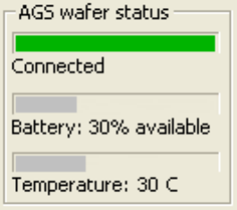
Chapter 3. Using Your AGS
3.20
•Red - No connection. Indicates that there is no connection between the gapping
wafer and link module. The values in the display do not update when the indicator is
red.
Figure 3.15: Wireless Connection Monitor
The Bluetooth wireless link technology used in the AGS is a low-power technology that
operates in the 2.4 GHz radio frequency band. This unlicensed band is also used by many other
types of devices, such as cordless phones and microwave ovens. Another 2.4 GHz device
operating in close proximity could interfere with the AGS system. When this happens,
separating the devices by at least 6 ft (2 m) usually solves the problem.
Other factors can also affect the wireless link, such as the distance between the gapping wafer
and link and obstacles between the gapping wafer and link that block the signal. If GapView
indicates that the connection isn’t good, try moving the link module a few feet closer to the
gapping wafer.
Changing the Pairing Between the Gapping
Wafer and Link
Each gapping wafer is paired with a specific link module at the factory and will operate only
with its paired link module. You can change this pairing so that you can use your gapping wafer
with a different AGS link module, or vice versa. Link modules for different CyberOptics
WaferSense products, such as Auto Leveling Sensors (ALS), are not interchangeable.
To pair a gapping wafer and link module:
1. If you are changing the pairing of a gapping wafer that is already paired with a link
module, first unplug the currently paired link module. You can’t pair a gapping wafer with
a new link module while the currently paired link module is powered on.
2. Make sure the Power lights are illuminated on both the gapping wafer and link module
you want to pair.
Chapter 3. Using Your AGS
3.21
3. On the gapping wafer, press and hold the PAIR button until the Pair Status and
Connection Status lights start to blink rapidly (about four times per second).
4. On the link module, press and hold the PAIR button until the Pair Status and
Connection Status lights start to blink rapidly (about four times per second).
The Pair Status and Connection Status lights will continue to blink until the gapping
wafer and link have established a new pairing, after which the lights will be on and no
longer blinking.
Saving Your Settings
Each time you exit the GapView application, it saves your current settings for the log file, target
gaps and tolerances, gap offsets, wafer display orientation, and gap units in the Windows
registry. The next time you start GapView, it restores those saved settings. You can also tell
GapView to save your settings to a file you specify, and you can have GapView read those
settings back at any time. This lets you have several different configurations for GapView and
be able to switch between them easily, without having to reenter the settings.
To save your settings in a file you specify:
1. Choose the File > Save Settings As menu item.
2. In the AGS Settings File dialog, specify the directory and file name and click Save.
GapView saves your settings, and the file you specified becomes the current settings file.
To save your settings in the current settings file:
• Choose the File > Save Settings menu item.
Each time you start GapView, the application automatically reads in the most recent settings
from the Windows registry, including the last settings file you specified, if any.
Loading Settings from a File
To load settings from a file:
1. Choose the File > Open Settings menu item.
2. In the AGS Settings File dialog, specify the directory and file name and click Open.
GapView reads the settings from the specified file and applies the settings. These settings
are also written to the Windows registry and will be loaded the next time you start the
GapView application.
4.1
Chapter 4
Maintaining Your AGS
Periodic calibration and battery replacement is the only regular maintenance your AGS requires:
•Annual Calibration and Battery Replacement. Once a year, you should have your
gapping wafer calibrated and the internal rechargeable battery replaced by returning
the gapping wafer to the CyberOptics Semiconductor factory.
•Field Calibration. In addition to the annual factory calibration, you should calibrate
your wafer using the field calibration procedure described in this chapter. Field
calibration is not a substitute for the annual factory calibration.
•Cleaning the Gapping Wafer. If cleaning is required, wipe the outside of the
gapping wafer with IPA (isopropyl alcohol). If the gapping wafer is used in a clean
environment, follow proper procedures for cleaning devices for this environment.
Warning
The edges of the AGS gapping wafer are thin. It may be possible to sustain an injury from
these edges if the gapping wafer is not handled with proper care.
Warning
Protection afforded by compliance to EN61010-1 (2001) may be impaired if the
equipment is not used as specified.
Warning
Do not immerse the gapping wafer or the link module in liquid. Do not spill liquids on
the gapping wafer or on the link module.
Chapter 4. Maintaining Your AGS
4.2
Annual Factory Calibration and Battery
Replacement
Every twelve months, you should return your gapping wafer to the CyberOptics
Semiconductor factory, where we will calibrate the gapping wafer and replace the internal
rechargeable battery. You can find the date when the gapping wafer was last calibrated at the
factory by choosing the Help > About your AGS Wafer menu item in the GapView
application. The date when the gapping wafer is due for its next calibration is shown on a label
affixed on the side of the raised center part of the gapping wafer.
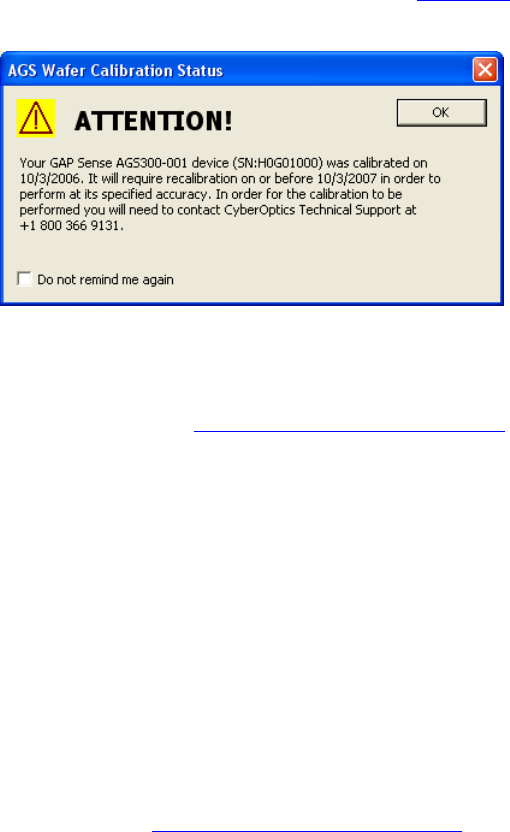
When the date for calibration approaches, the GapView application will occasionally notify you
by displaying the Wafer Calibration Status dialog, as shown in Figure 4.1.
Figure 4.1: Wafer Calibration Status Dialog
If you drop the gapping wafer or suspect that it is no longer in calibration, contact CyberOptics
Semiconductor technical support (see “Technical Support,” on page 2.9).
Battery Use and Disposal
Your AGS gapping wafer contains a lithium-polymer battery. To avoid damage to the gapping
wafer, use the supplied charger only. Do not charge the gapping wafer at temperatures outside
the specified range (0 °C to 45 °C). Do not incinerate or dispose of the gapping wafer into fire.
Do not immerse the gapping wafer when cleaning or spill liquids on the gapping wafer.
For proper battery disposal, please return the gapping wafer to CyberOptics Semiconductor,
Inc.:
CyberOptics Semiconductor, Inc.
13555 S.W. Millikan Way
Beaverton, OR 97005
or contact customer support (see “Technical Support,” on page 2.9).
Chapter 4. Maintaining Your AGS
4.3
Field Calibrating Your AGS
Over time, AGS gap measurements can drift. In addition to the annual factory calibration, you
might want to calibrate your AGS system periodically. GapView includes a field calibration
feature to make it easy to calibrate the AGS system. For this calibration, you’ll also need a
calibration fixture, which is available from CyberOptics. For information on the CyberOptics
fixture, contact Technical Support.
To field calibrate your AGS:
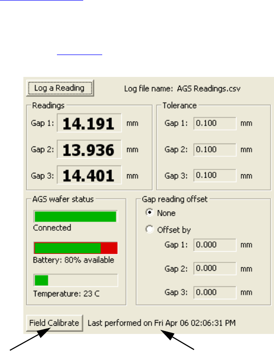
1. In GapView, the last time the AGS was field calibrated is shown to the right of the Field
Calibrate button (see Figure 4.2). Click Field Calibrate to start the calibration wizard.
Figure 4.2: Field Calibrate Button and Last Calibration
Date of last field calibrationField Calibrate button
Chapter 4. Maintaining Your AGS
4.4
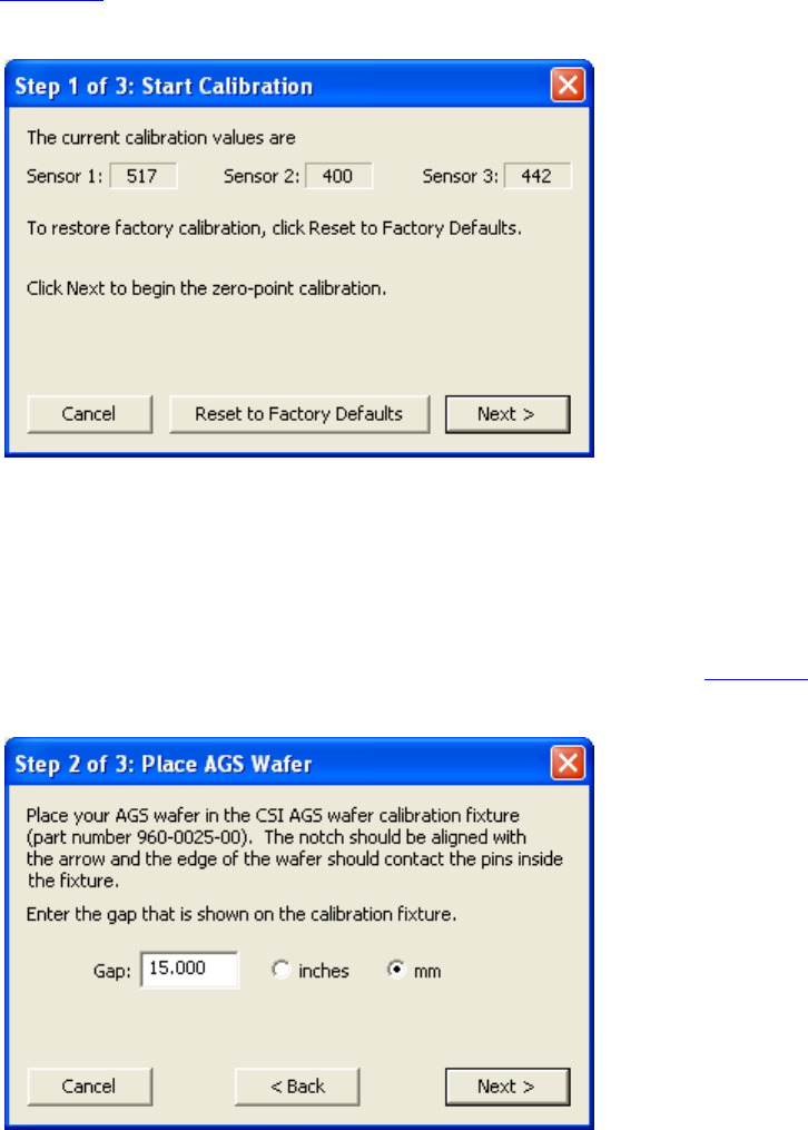
The Calibration wizard is displayed showing the Step 1 of 3 Start Calibration dialog, as
shown in Figure 4.3.
Figure 4.3: Step 1 of 3 Start Calibration Dialog
This dialog displays the current calibration values. Clicking Reset to Factory Defaults
the last factory calibration setting.
2. Click Next to continue with the calibration procedure.
The wizard now displays the Step 2 of 3 Place AGS Wafer dialog, as shown in Figure 4.4.
Figure 4.4: Step 2 of 3 Place AGS Wafer Dialog
Chapter 4. Maintaining Your AGS
4.5
3. Follow the instructions in Step 2 of the wizard to place the gapping wafer in the
calibration fixture. In the Gap box, enter the gap distance for the fixture, which is shown
on the fixture.
4. When you have completed Step 2, click Next.
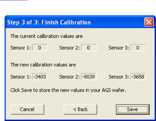
After a few seconds, the wizard displays the Step 3 of 3 Finish Calibration dialog, as
shown in Figure 4.5.
Figure 4.5: Step 3 of 3 Finish Calibration Dialog
This dialog shows the current calibration values (the values from the last factory or field
calibration) and the new values that were just determined in this calibration. At this point,
the new values have not been saved to the gapping wafer.
5. Click Save to save the new calibration values.
6. That completes the field calibration.

5.1
Chapter 5
Specifications
System Requirements
To run the WaferSense AGS software and link, your computer must have:
• Windows 2000, Windows XP, or Windows Vista operating system
• One free high-power USB 1.1 or USB 2.0 port
AGS Hardware
Environmental
Operating pressure range: 760 to less than 10-6 Torr.
Storage temperature range: -20 °C to 45 °C.
Charging temperature range: 0 °C to 45 °C.
Operating temperature range: 20 °C to 70 °C.
Power
Battery charger requires 100 - 240 VAC at 47 - 63 Hz input.
Battery usage on a full charge: approximately 4 hours.
Typical battery recharge cycles: approximately 500.
Range and Accuracy
Range: 0.35" to 0.79" (9 mm to 20 mm).
Parallelism accuracy: ±0.025 mm (0.001") with gap of 15 mm (0.6").
Gap accuracy: ±0.25 mm (0.01") with gap of 15 mm (0.6").

Index.1
Index
A
About GapView dialog 2.9
About your AGS Wafer dialog 2.9
accuracy of measurements 4.2, 4.3, 5.1
adjusting readings 3.10
AGS
installing 2.1
see also gapping wafer
specifications 5.1
system components 1.1
automatic shutoff, gapping wafer 2.5, 3.3
B
battery 3.18
care and disposal 4.2
recharging 3.18
replacement 4.1, 4.2
specifications 5.1
Bluetooth wireless link 1.1, 3.20
buttons on gapping wafer 3.3
C
calibration
date of last 2.9, 4.3
factory 4.2
field 4.3
fixture 4.3
case, see clean box
Charging Done status light 3.3
Charging status light 3.3
clean box
opening and closing 3.2
recharging the battery 3.18
cleaning the gapping wafer 4.1
Comment, including in log file 3.14
components, AGS 1.1
Connection Status light 3.3
D
displaying log entries 3.15
E
electrostatic discharge ii
ESD ii
F
factory calibration 4.2
FCC standards ii
field calibration 4.3
fixture, calibration 4.3
G
gap measurement 3.4
gap offsets 3.10
gap readouts 3.7
gapping wafer
automatic shutoff 2.5, 3.3
battery replacement 4.1
buttons 3.3, 3.21
calibration 4.2
changing pairing with link module 3.20
cleaning 4.1
field calibration 4.3
maintenance 4.1
monitoring the connection 3.19
recharging the battery 3.18
Index
Index.2
gapping wafer (cont.)
registering 2.6
serial number 2.9
status lights 2.5, 3.3, 3.20, 3.21
GapView
main window 3.5
software installation 2.1
starting the application 2.7
version 2.9
H
hardware specifications 5.1
I
inch units 3.9, 3.10
installation
AGS 2.1
link module 2.3
software 2.1
system requirements 2.1
L
link module
changing pairing with gapping wafer 3.20
installation 2.3
monitoring the connection 3.19
PAIR button 3.21
status lights 2.4, 2.5, 3.20, 3.21
USB port 2.1
Log a Reading button 3.13
log file 3.15
logging readings 3.13
Comment 3.14
displaying log entries 3.15
log file 3.15
Operator 3.14
Station 3.14
Tool 3.14
user-specified information 3.14
M
maintaining the gapping wafer 4.1
measurement offsets 3.10
measurement range and accuracy 5.1
millimeter units 3.9, 3.10
monitoring the wireless connection 3.19
N
notch location 3.12
O
offsets 3.10
ON / OFF button 2.5, 3.3
operating temperature
monitoring 3.17
specifications 5.1
Operator, including in log file 3.14
orientation of wafer 3.12
P
PAIR button 3.3, 3.21
Pair Status light 3.3
pairing of gapping wafer and link module,
changing 3.20
Power status light 3.3
preferences, see settings
pressure range 5.1
printing 3.16
R
radio interference ii
range of measurements 5.1
reading offsets 3.10
rechargeable battery
recharging 3.18
rechargeable battery, see battery
registering your gapping wafer 2.6
rotating the wafer display 3.12
Index
Index.3
S
saving settings 3.21
serial number, gapping wafer 2.9
settings
gap criteria 3.9
gap offsets 3.10
log file 3.15
saving 3.21
wafer display orientation 3.12
shutoff, automatic 2.5, 3.3
software installation 2.1
software version 2.9
specifications 5.1
starting GapView 2.7
Station, including in log file 3.14
status lights
gapping wafer 2.5, 3.3, 3.20, 3.21
link module 2.4, 2.5, 3.20, 3.21
support 2.9
T
technical support 2.9
temperature
monitoring 3.17
specifications 5.1
Tool, including in log file 3.14
U
units, mm or inches 3.9, 3.10
USB port 2.1, 2.3
V
version of software 2.9
W
Windows operating system 2.1
wireless link, see link module
wireless technology 3.20