CyberTAN Technology WD105 1x1 802.11b/g/n module User Manual
CyberTAN Technology Inc. 1x1 802.11b/g/n module
User Manual.pdf
Confidential i 2014-03-18
WD105
Datasheet
CyberTAN Technology, Inc.
Model Name WD105
Description 802.11n LGA IoE Module
Version Release 0.3a
Date March 20, 2014
Author Cindy Fan
WD105
Datasheet
2014-03-20
1
Revision History
Date Release Author Description
2013-06-11 0.1 Cindy Fan First preliminary release.
2013-06-18 0.2 Cindy Fan Engineering Release.
2013-08-23 0.2a Cindy Fan Temporary Engineering Revision.
2014-03-18 0.3 Cindy Fan Update §4. Mechanical Characteristics.
2014-03-20 0.3a Cindy Fan Add §8. Regulatory Information
Related Documents
Date Author Description
Qualcomm Atheros QCA4002 datasheet
IEEE.org IEEE 802.11b/g/n specifications
CyberTAN Technology, Inc.
No. 99, Park Avenue III
Hsinchu Science Park
Hsinchu, Taiwan 30077
R.O.C.
CyberTAN® is a registered trademark of CyberTAN Technology, Inc. Bluetooth® is a trademark of the Bluetooth SIG.
All other trademarks appearing herein are the property of their respective owners.
This document may contain privileged or confidential information that is the property of CyberTAN Technology, Inc.
and the improper disclosure of which is an offense punishable under law. This document may be viewed and used only
by the individual or other entity that received it directly from CyberTAN. Redistribution of this document in any form
is strictly prohibited.
The products described in this document are not intended or designed for use in any application involving risk of harm
to persons or property. CYBERTAN PROVIDES THIS DOCUMENT AS-IS, WITHOUT WARRANTY OF ANY
KIND. CYBERTAN DISCLAIMS ALL WARRANTIES, EXPRESSED AND IMPLIED, INCLUDING, WITHOUT
LIMITATION, THE IMPLIED WARRANTIES OF MERCHANTABILITY, FITNESS FOR A PARTICULAR
PURPOSE, AND NON-INFRINGEMENT.

WD105
Datasheet
2014-03-20
2
Table of Contents
1.INTRODUCTION ................................................................................................................................................ 4
2.FEATURES .......................................................................................................................................................... 4
3. SPECIFICATION ................................................................................................................................................. 5
4. MECHANICAL CHARACTERISTICS ............................................................................................................. 7
4.1 MODULE DIMENSIONS .......................................................................................................................................... 7
4.2 PIN OUT DEFINITIONS .......................................................................................................................................... 8
4.3 PAD NUMBERINGS ................................................................................................................................................ 9
4.4 PAD SIZE ............................................................................................................................................................ 10
4.5 PIN DEFINITIONS ................................................................................................................................................ 11
5. BLOCK DIAGRAM ............................................................................................................................................. 14
6. WARRANTY ......................................................................................................................................................... 14
7. PACKAGE AND ASSEMBLY NOTES ............................................................................................................... 15
7.1 REEL SPECIFICATIONS ........................................................................................................................................ 15
7.2 CARRIER SPECIFICATIONS .................................................................................................................................. 15
7.3 TAPE PET COVER SPECIFICATION ...................................................................................................................... 16
7.4 TAPE PROTECTION RIBBON ................................................................................................................................ 16
7.5 PACKING INSTRUCTION ...................................................................................................................................... 16
7.6 ALUMINUM BAG LABEL ..................................................................................................................................... 18
7.7 WHITE BOX LABEL AND ALUMINUM BAG LABEL .............................................................................................. 18
7.8 CARTON LABEL .................................................................................................................................................. 18
7.9 PALLET SPECIFICATION ................................................................................................................................... 19
8. REGULATORY INFORMATION ...................................................................................................................... 21
8.1 FCC NOTICE (USA) ........................................................................................................................................... 21
8.2 FCC LABELING REQUIREMENTS ...................................................................................... 錯誤! 尚未定義書籤。
8.3 RF EXPOSURE .................................................................................................................. 錯誤! 尚未定義書籤。
8.4 INDUSTRY CANADA NOTICE ............................................................................................................................... 23

WD105
Datasheet
2014-03-20
3
List of Figures
FIGURE 1: PCB OUTLINE TOP VIEW (UNIT: MM) ........................................................................................................ 7
FIGURE 2: PIN OUT CONFIGURATION........................................................................................................................... 8
FIGURE 3: PAD LAYOUT (TOP VIEW) .......................................................................................................................... 9
FIGURE 4: PAD SIZE TOP VIEW (UNIT: MM) .............................................................................................................. 10
FIGURE 5: BLOCK DIAGRAMN ................................................................................................................................... 14
List of Tables
TABLE 1: PIN DEFINITIONS ....................................................................................................................................... 11
TABLE 1-1: PIN DEFINITIONS : SPI ............................................................................................................................ 12
TABLE 1-2: PIN DEFINITIONS : SDIO ........................................................................................................................ 12
TABLE 1-3: PIN DEFINITIONS : I2S ............................................................................................................................ 13
TABLE 1-4: PIN DEFINITIONS : JTAG ........................................................................................................................ 13
TABLE 1-5: PIN DEFINITIONS : HOST INTERFACES .................................................................................................... 13
TABLE 2: WHITE BOX LABEL SPECIFICATION ......................................................................................................... 18
TABLE 3: CARTON LABEL SPECIFICATION ............................................................................................................... 18
TABLE 4: PALLET DIMENSIONS SPECIFICATION ....................................................................................................... 19
TABLE 5: MAX. HEIGHT SPECIFICATION .................................................................................................................. 19

WD105
Datasheet
2014-03-20
4
1. Introduction
WD105 is IoE Smart Network module that enables wireless internet connectivity for any device
wishing to be monitored or managed remotely. The WD105 is architected for ultra-low power
consumption, with near-zero power consumption in power down modes with fast wakeup.
2. Features
• Fast wake up when loading firmware from inexpensive external NVMEM (SPI flash
device)
• Direct connect to a 50-Ω antenna
• Standard interfaces: SPI slave and GPIO
• On-SIP integrated IPv4/Ipv6 stack reduces CPU and Flash requirements on host
microcontroller.
• On-Board 4Mb flash to accommodate firmware.
• BSD-like interface provides a common easy interface across different operating systems,
simplifying porting of the IP Stack offload
• TCP or UDP operation
• Compatible with IEEE 802.11b/g and 802.11n standard.

WD105
Datasheet
2014-03-20
5
3. Specification
Model Number WD105
Product Type 802.11n perforation IoE module
Memory Size 4Mbit of Flash
Host Interface(s) SPI, HSIC, USB2.0, SDIO (selectable, see Table 1-5)
Embedded MAC Address Yes
WiFi Chip(s) Qualcomm Atheros QCA4002
Package 27-pin perforation
Wireless Standard(s) IEEE 802.11b/g/n
Spreading IEEE 802.11b DSSS and 802.11g/n OFDM
Operating Frequency 2412~2484MHz ISM band
Antenna On-board PCB antenna. (On request an I-PEX plug leading
to an external antenna can be made available)
Number of Channels 11 (US), 13 (EU), 14 (Japan)
Data Rates 802.11n: up to 72.2Mbps
802.11g: 54Mbps with fallback to 48,36,24,18,12,9 and
6Mbps
802.11b: 11Mbps with fallback to 5.5, 1 and 1Mbps
Modulation Schemes 802.11g/n:
64QAM (up to 72.2Mbps),
16QAM (39/36/26/24Mbps),
QPSK (19.5/18/13/12Mbps),
BPSK (9/6.5/6Mbps)
802.11b:
CCK (11/5.5Mbps), DQPSK (2Mbps), DBPSK (1Mbps)
Tx Power (typical) 18dBm for 802.11b
14dBm for 802.11g
13dBm for 802.11n (MSC7)
Rx Sensitivity (typical) -92dBm for 1Mbps @ 8% PER
-85dBm for 11Mbps @ 8% PER
-72dBm for 54Mbps @ 10% PER
-69dBm for HT20, MCS7 @ 10% PER
Media Access Protocol CSMA/CA with ACK
Operating System Support Not Applicable. Controlled with a command set.
Tx Power (average)

WD105
Datasheet
2014-03-20
6
Model Number WD105
Power Requirements (typical) Tx mode :
11Mbps: 240mA
54Mbps: 210mA
72.2Mbps: 220mA
Rx mode :
11Mbps: 62mA
54Mbps: 62mA
72.2Mbps: 62mA
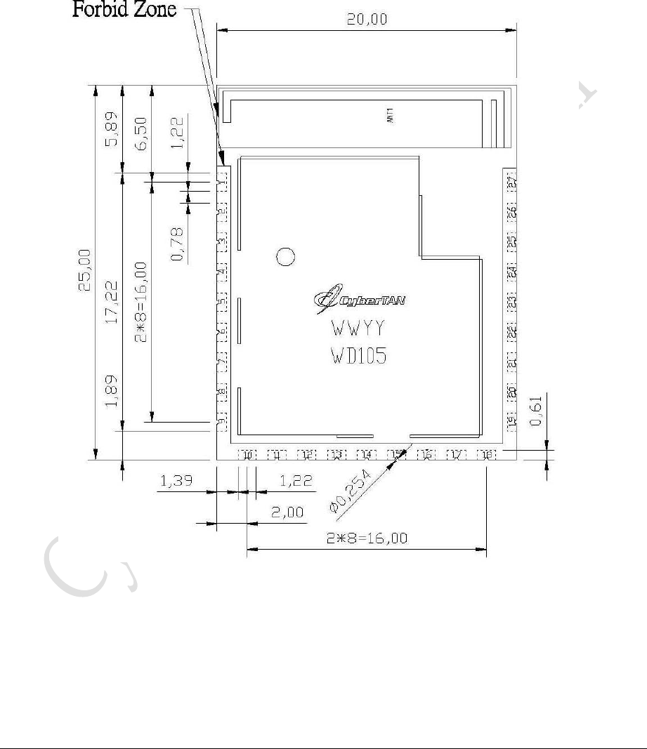
Dimensions 25 x 20 x 2.6 ±0.25 mm (typical)
Regulatory Conformance FCC Part 15b, Part 15c
RoHS Compliance Yes
Operating Temperatures 0 ~ 70oC
Software Functions n/a
WD105
Datasheet
2014-03-20
7
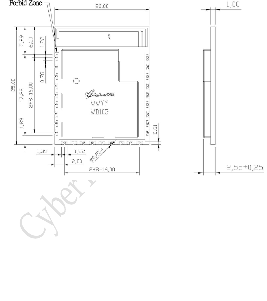
4. Mechanical Characteristics
4.1 Module Dimensions
Figure 1: PCB Outline Top View (Unit: mm)
WD105
Datasheet
2014-03-20
8
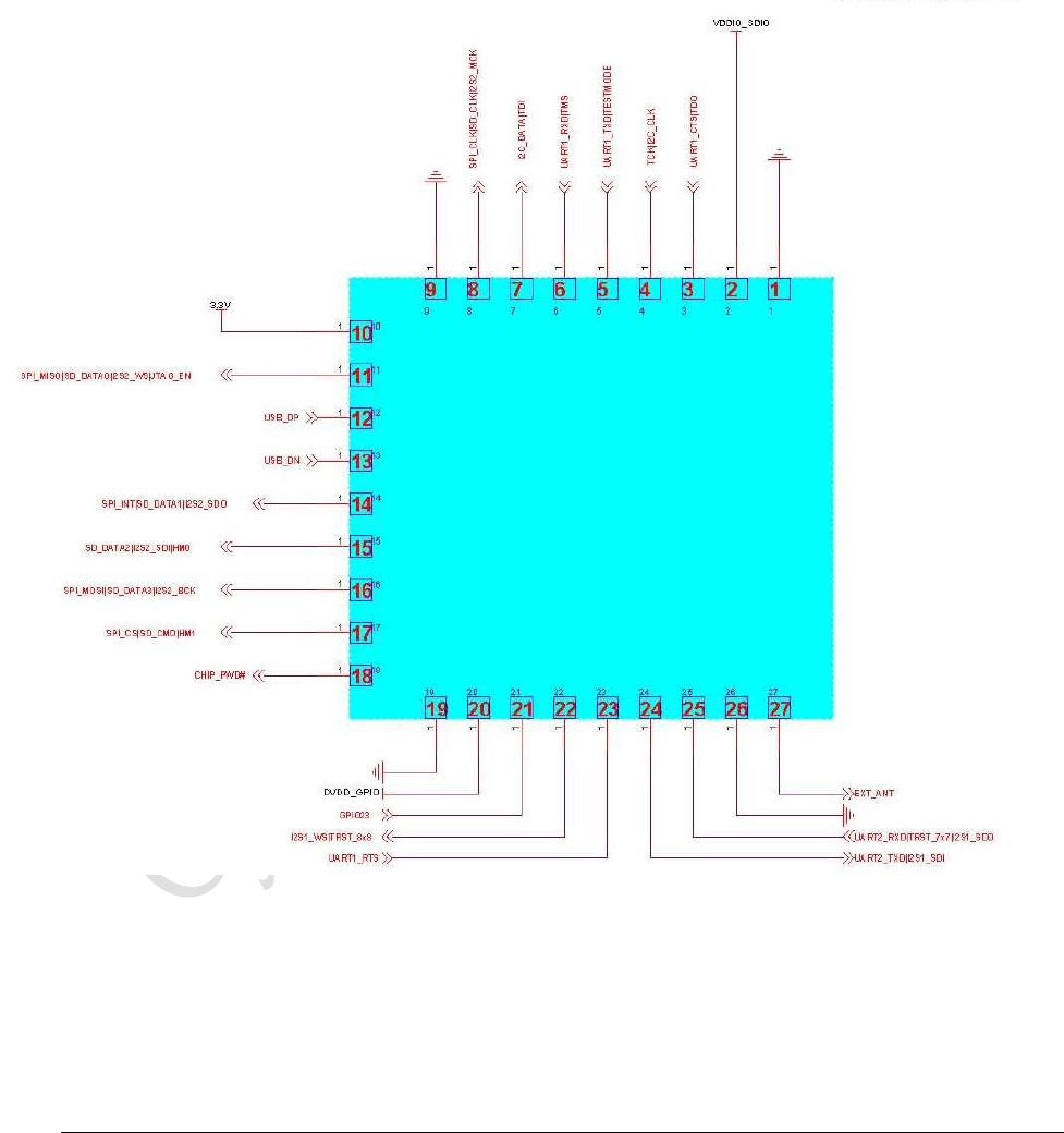
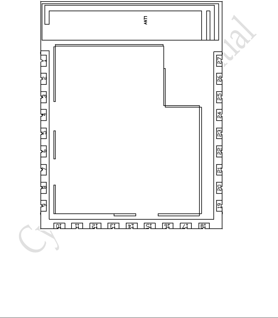
4.2 Pin Out Definitions
The logical definitions of the module’s pins are depicted below.
Figure 2: Pin out Configuration
WD105
Datasheet
2014-03-20
9
4.3 Pad Numberings
Pin numbers are defined according to the following map.
Figure 3: Pad Layout (Top View)
WD105
Datasheet
2014-03-20
10
4.4 Pad Size
Pin numbers are defined according to the following map.
Figure 4: Pad Size Top View (Unit: mm)

WD105
Datasheet
2014-03-20
11
4.5 Pin Definitions
This section describes module signals and the associated pins.
Table 1: Pin Definitions
Pin No. Pin name Description Genernal Type
1 Ground Ground P
2 VDDIO_SDIO Connect to 3.3V host I/O supply or 1.8V peripheral I/O supply P
3 UART1_CTS|TDO UART Clear to Send O
4 TCK|I2C_CLK I2C Clock I/O
5 UART1_TXD|TESTMODE UART1 Series Output. O
6 UART1_RXD|TMS UART1 Series intput. I
7 I2C_DATA|TDI I2C DATA I/O
8 SPI_CLK|SD_CLK|I2S2_MCK
9 Ground Ground P
10 3.3V Connect to 3.3V supply P
11
SPI_MISO|SD_DATA0|I2S2_WS|JTA
G_EN
12 USB_DP
USB D+ signal; carries USB data to and from the USB 2.0
PHY
IA/OA
13 USB_DN
USB D- signal; carries USB data to and from the USB 2.0
PHY
IA/OA
14 SPI_INT|SD_DATA1|I2S2_SDO
15 SD_DATA2|I2S2_SDI|HM0
16 SPI_MOSI|SD_DATA3|I2S2_BCK
17 SPI_CS|SD_CMD|HM1
18 CHIP_PWD# Chip power-down control I
19 Ground Ground P
20 DVDD_GPIO Connect to 3.3V host I/O supply or 1.8V peripheral I/O supply P
21 GPIO23 General purpose input/output 23 I/O
22 I2S1_WS|TRST_8x8
23 UART1_RTS Bluetooth UART Request to Send. O
WD105
Datasheet
2014-03-20
12
Pin No. Pin name Description Genernal Type
24 UART2_TXD|I2S1_SDI UART2 Series Output. O
25 UART2_RXD|TRST_7x7|I2S1_SDO UART2 Series Input. I
26 Ground Ground P
27 EXT_ANT option for external RF path, default not enable RF I/O
Table 1-1: Pin Definitions : SPI
Pin No. Pin name Host Interface
function1-SPI function1 type
8 SPI_CLK|SD_CLK|I2S2_MCK SPI Clock I/O
11 SPI_MISO|SD_DATA0|I2S2_WS|JTAG_EN SPI MISO O
14 SPI_INT|SD_DATA1|I2S2_SDO SPI INT I/O
16 SPI_MOSI|SD_DATA3|I2S2_BCK SPI MOSI I
17 SPI_CS|SD_CMD|HM1 SPI CS I
Table 1-2: Pin Definitions : SDIO
Pin No. Pin name Host Interface function1-SDIO function2 type
8 SPI_CLK|SD_CLK|I2S2_MCK SDIO Clock I/O
11 SPI_MISO|SD_DATA0|I2S2_WS|JTAG_EN SDIO Data Line 0. I/O
14 SPI_INT|SD_DATA1|I2S2_SDO SDIO Data Line 1. I/O
15 SD_DATA2|I2S2_SDI|HM0 SDIO Data Line 2. I/O
16 SPI_MOSI|SD_DATA3|I2S2_BCK SDIO Data Line 3. I/O
17 SPI_CS|SD_CMD|HM1 SDIO command line I/O
WD105
Datasheet
2014-03-20
13
Table 1-3: Pin Definitions : I2S
Pin No. Pin name Interface function3 function3 type
8 SPI_CLK|SD_CLK|I2S2_MCK I2S2 MCK I/O
11 SPI_MISO|SD_DATA0|I2S2_WS|JTAG_EN I2S2 WS
14 SPI_INT|SD_DATA1|I2S2_SDO I2S2_SDO O
15 SD_DATA2|I2S2_SDI|HM0 I2S2_SDI I
16 SPI_MOSI|SD_DATA3|I2S2_BCK I2S2_BCK I/O
22 I2S1_WS|TRST_8x8 I2S1_WS I
24 UART2_TXD|I2S1_SDI I2S1_SDI I
25 UART2_RXD|TRST_7x7|I2S1_SDO I2S1_SDO O
Table 1-4: Pin Definitions : JTAG
Pin No. Pin name debug
function4 function4
type Bootstrap function4
3 UART1_CTS|TDO TDO I
4 TCK|I2C_CLK TCK I/O
5 UART1_TXD|TESTMODE
JTAG mode: TESTMODE,pull high
through 10 kohm to VDDIO_SDIO for
JTAG mode enable
6 UART1_RXD|TMS TMS I
7 I2C_DATA|TDI TDI I
11 SPI_MISO|SD_DATA0|I2S2_WS|JTAG_EN
JTAG mode: JTAG_EN ,pull high
through 10 kohm to VDDIO_SDIO for
JTAG mode enable
Table 1-5: Pin Definitions : Host Interfaces
Pin No. Pin name debug
function4 function4
type Bootstrap function4
15 SD_DATA2|I2S2_SDI|HM0 HM0: Host selection mode0
17 SPI_CS|SD_CMD|HM1 HM1: Host selection mode1
WD105
Datasheet
2014-03-20
14
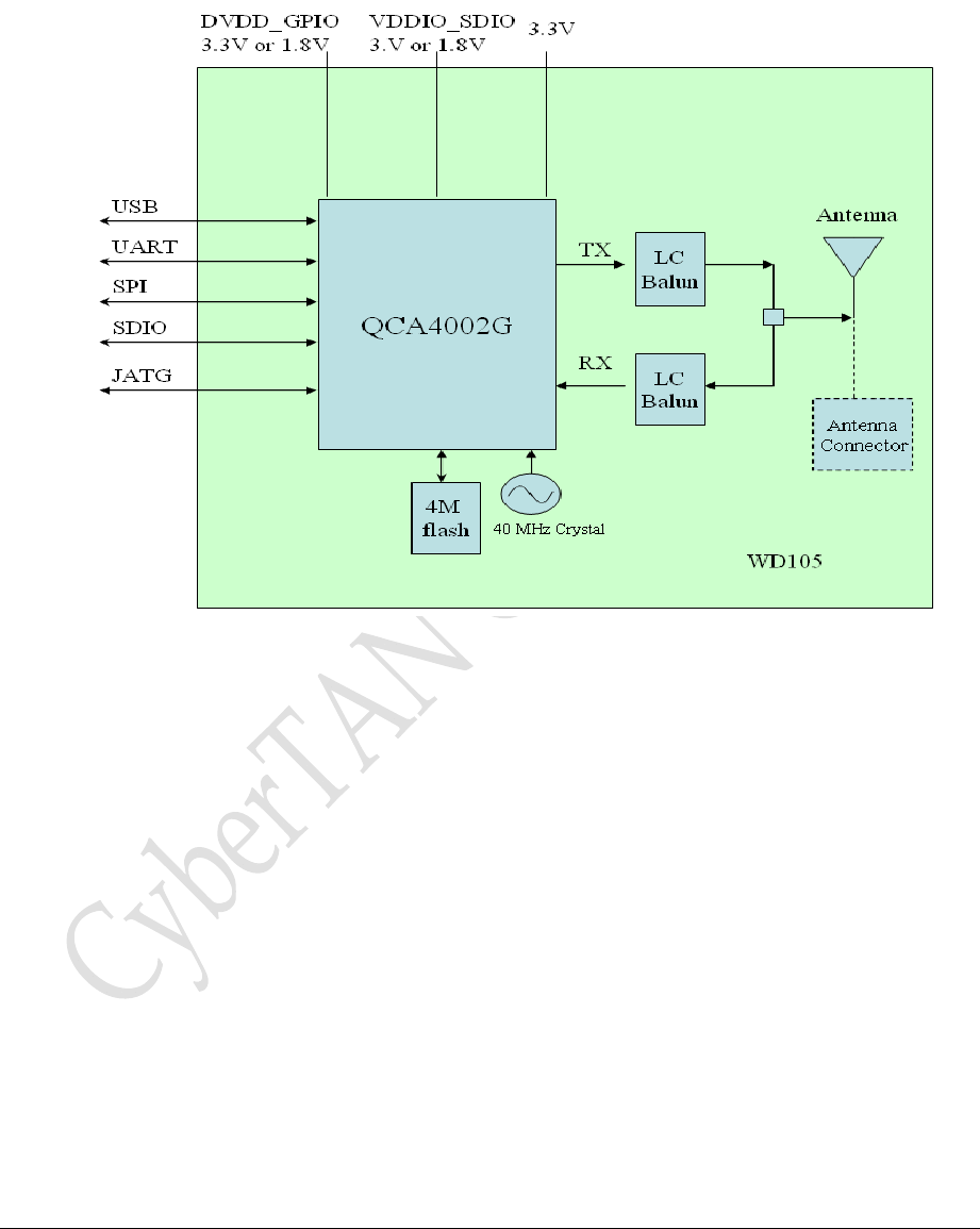
5. Block Diagram
Figure 5: Block Diagramn
6. Warranty
One year limited warranty.

WD105
Datasheet
2014-03-20
15
7. Package and Assembly Notes
7.1 Reel Specifications
The following diagram depicts the reel specifications in shipping WD105.
(TBD)
Figure 6: Reel Specifications
7.2 Carrier Specifications
The following diagram depicts the carrier specifications in shipping WD105.
(TBD)
Figure 7: Carrier Specifications

WD105
Datasheet
2014-03-20
16
7.3 Tape PET Cover Specification
The following diagram depicts the Tape PET Cover specification in shipping WD105.
(TBD)
Figure 8: Tape PET Cover Specification
7.4 Tape Protection Ribbon
The following diagram depicts the Tape Protection Ribbon specification in shipping WD105.
(TBD)
Figure 9: Tape Protection Ribbon
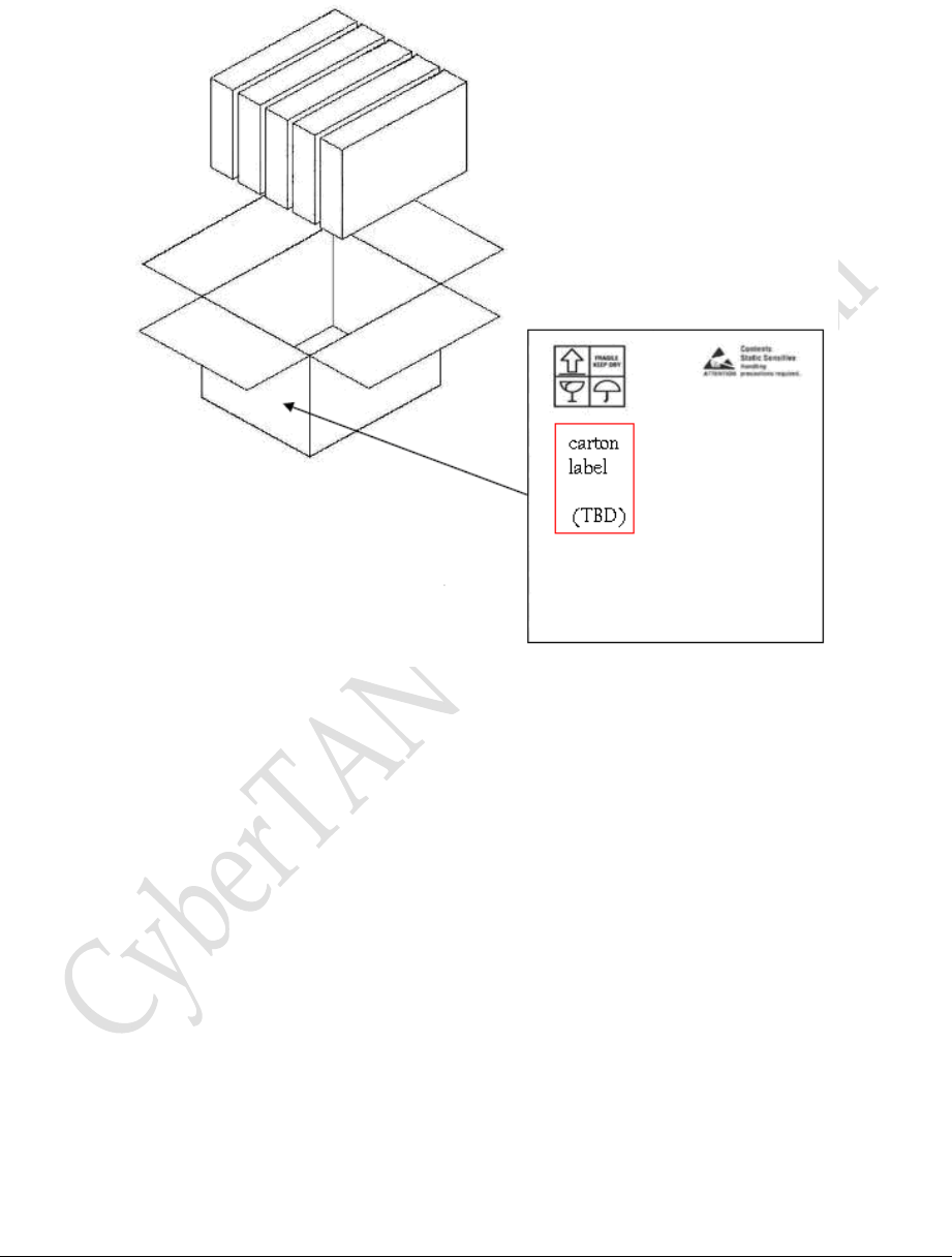
7.5 Packing Instruction
The following diagram depicts the packing instruction specification in shipping WD105.
WD105
Datasheet
2014-03-20
17
Figure 10: Packing Instruction

WD105
Datasheet
2014-03-20
18
7.6 Aluminum Bag Label
The following diagram depicts the Aluminum bag label specification in shipping WD105.
(TBD)
Figure 11: Aluminum Bag Label 1
7.7 White Box Label and Aluminum Bag Label
(TBD)
Figure 12: Box Label
Table 2: White Box Label Specification (TBD)
7.8 Carton Label
(TBD)
Figure 13: Carton Label
Table 3: Carton Label Specification (TBD)
WD105
Datasheet
2014-03-20
19
7.9 Pallet Specification
7.9.1 Pallet Dimensions
The following table the pallet specification in shipping WD105.
Table 4: Pallet Dimensions Specification
Shipping ways Pallet Size W x L x H
Air Shipment 113cm x 120cm x 12cm (recommended)
Sea Shipment 113cm x 120cm x 12cm (recommended)
7.9.2 Max. Height
The following table the max. height specification in shipping WD105.
Table 5: Max. Height Specification
Shipping ways Height Limitation (including pallet height)
Air Shipment Less than150cm
Sea Shipment Less than190cm
WD105
Datasheet
2014-03-20
20
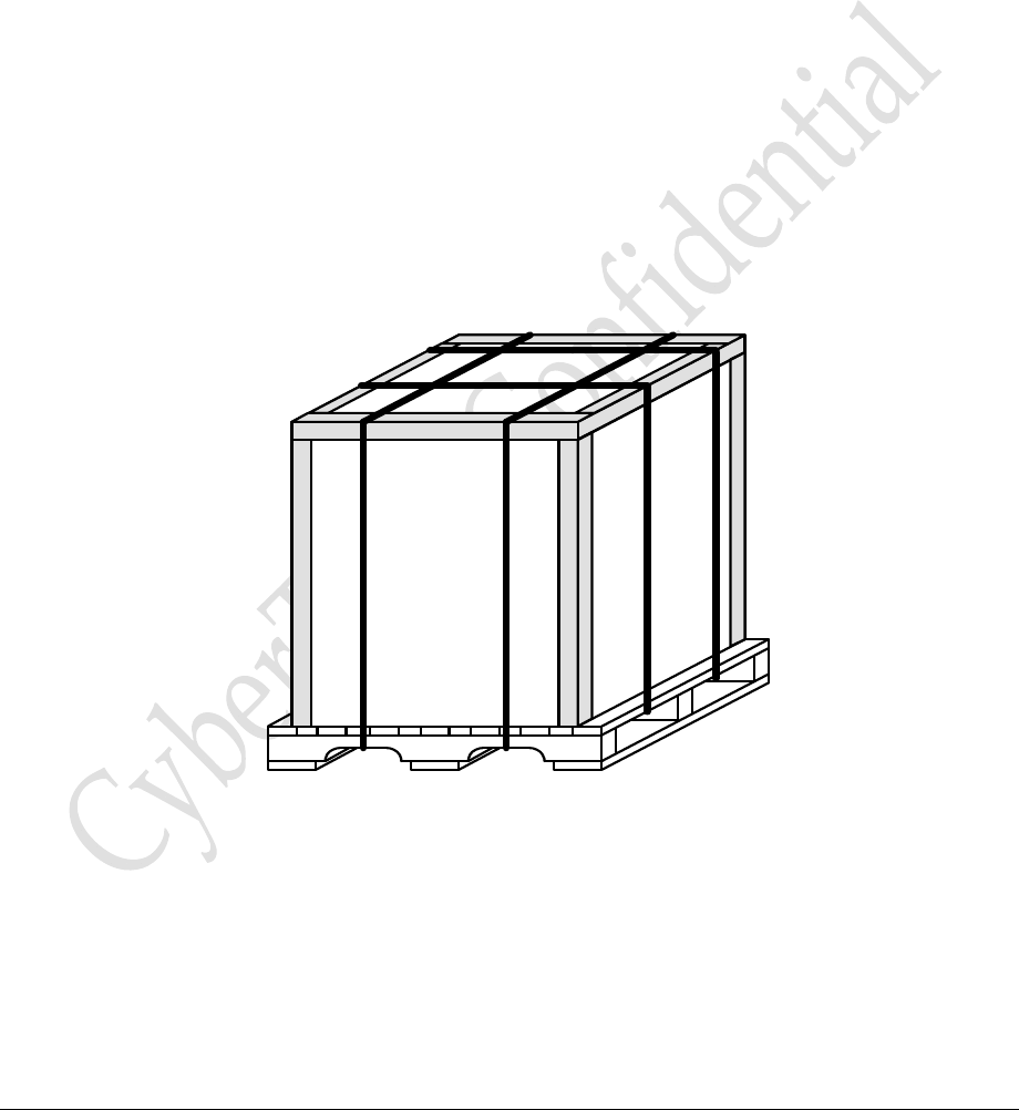
7.9.3 Pallet Packaging
a). V-boards and strapping:
a-1. Put 4 V-boards on the four side corners to prevent cartons collapse.
a-2. Put 4 V-boards on the four top edges.
a-3. Fix the unit by at least 2 pieces of PP straps.
b). Wrapping:
b-1. Put 3 layers at least on each surface.
b-2. Carton logo need to be recognized
if over 3 layers.
b-3. Make sure not to tighten too much
as it can damage he loads.
b-4. Need to seal the top layer with wrap.
V-boards and Strapping
4-way strapping, V-boards on side
corner and top edges

WD105
Datasheet
2014-03-20
21
8. Regulatory Information
8.1 FCC Notice (USA)
This device complies with Part 15 of the FCC Rules. Operation is subject to the following two conditions: (1) This
device may not cause harmful interference, and (2) this device must accept any interference received, including
interference that may cause undesired operation.
This equipment has been tested and found to comply with the limits for a Class B digital device, pursuant to Part
15 of the FCC Rules. These limits are designed to provide reasonable protection against harmful interference in a
residential installation. This equipment generates, uses and can radiate radio frequency energy and, if not installed
and used in accordance with the instructions, may cause harmful interference to radio communications. However,
there is no guarantee that interference will not occur in a particular installation. If this equipment does cause
harmful interference to radio or television reception, which can be determined by turning the equipment off and on,
the user is encouraged to try to correct the interference by one of the following measures:
- Reorient or relocate the receiving antenna.
- Increase the separation between the equipment and receiver.
- Connect the equipment into an outlet on a circuit different from that
to which the receiver is connected.
- Consult the dealer or an experienced radio/TV technician for help.
FCC Caution: Any changes or modifications not expressly approved by the party responsible for compliance could
void the user's authority to operate this equipment.
This transmitter must not be co-located or operating in conjunction with any other antenna or transmitter.
Radiation Exposure Statement:
This equipment complies with FCC radiation exposure limits set forth for an uncontrolled environment. This
equipment should be installed and operated with minimum distance 20cm between the radiator & your body.

WD105
Datasheet
2014-03-20
22
This device is intended only for OEM integrators under the following conditions:
1) The antenna must be installed such that 20 cm is maintained between the antenna and users, and
2) The transmitter module may not be co-located with any other transmitter or antenna.
As long as 2 conditions above are met, further transmitter test will not be required. However, the OEM
integrator is still responsible for testing their end-product for any additional compliance requirements required
with this module installed
IMPORTANT NOTE: In the event that these conditions can not be met (for example certain laptop
configurations or co-location with another transmitter), then the FCC authorization is no longer considered valid
and the FCC ID can not be used on the final product. In these circumstances, the OEM integrator will be
responsible for re-evaluating the end product (including the transmitter) and obtaining a separate FCC
authorization.
End Product Labeling
This transmitter module is authorized only for use in device where the antenna may be installed such that 20 cm
may be maintained between the antenna and users. The final end product must be labeled in a visible area with
the following: “Contains FCC ID: N89-WD105”. The grantee's FCC ID can be used only when all FCC
compliance requirements are met.
Manual Information To the End User
The OEM integrator has to be aware not to provide information to the end user regarding how to install or
remove this RF module in the user’s manual of the end product which integrates this module. The end user
manual shall include all required regulatory information/warning as show in this manual.

WD105
Datasheet
2014-03-20
23
8.4 Industry Canada Notice
(TBD)