Cypress Semiconductor 3025 Bluetooth Module User Manual CYBT 013033 01 EZ BT Module
Cypress Semiconductor Bluetooth Module CYBT 013033 01 EZ BT Module
UserManual.wiki
>
Cypress Semiconductor
>
3025 User Manual
User Manual
Navigation menu
Upload a User Manual
Namespaces
Wiki Guide
HTML
PDF
Info
Views
User Manual
Discussion / Help
Navigation
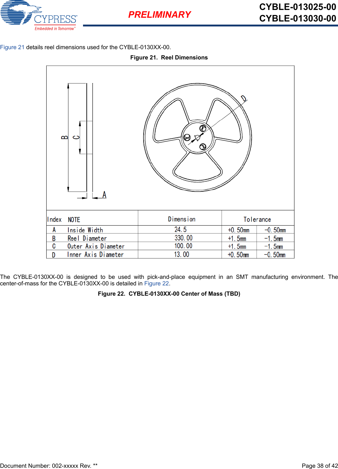
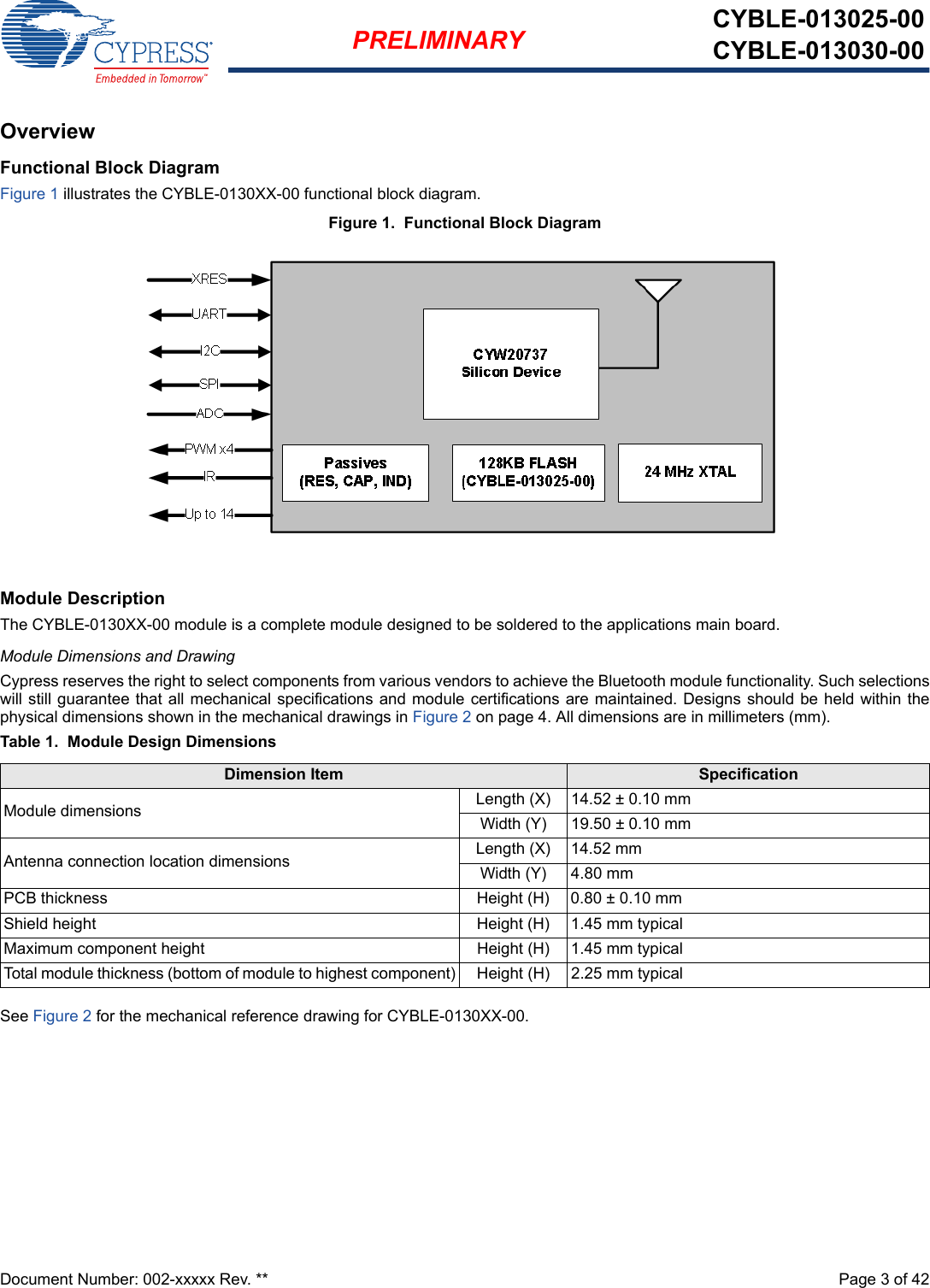
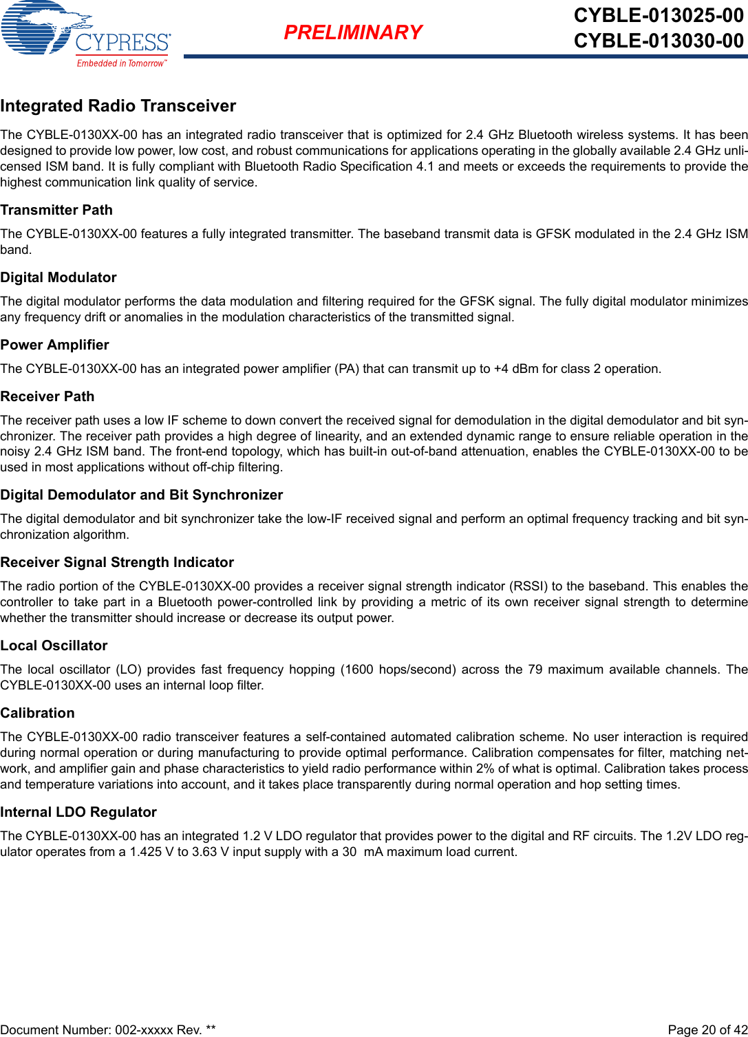
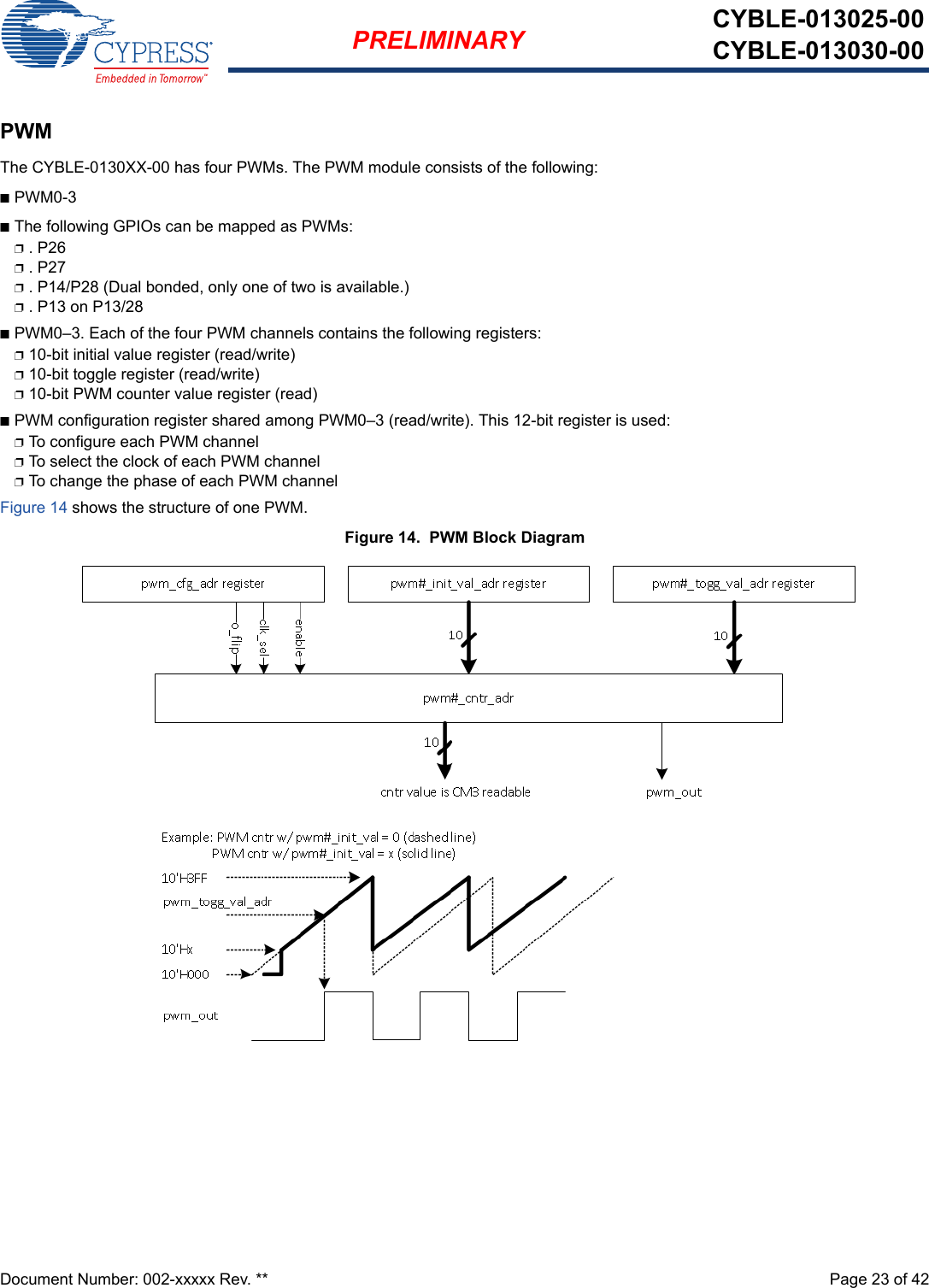
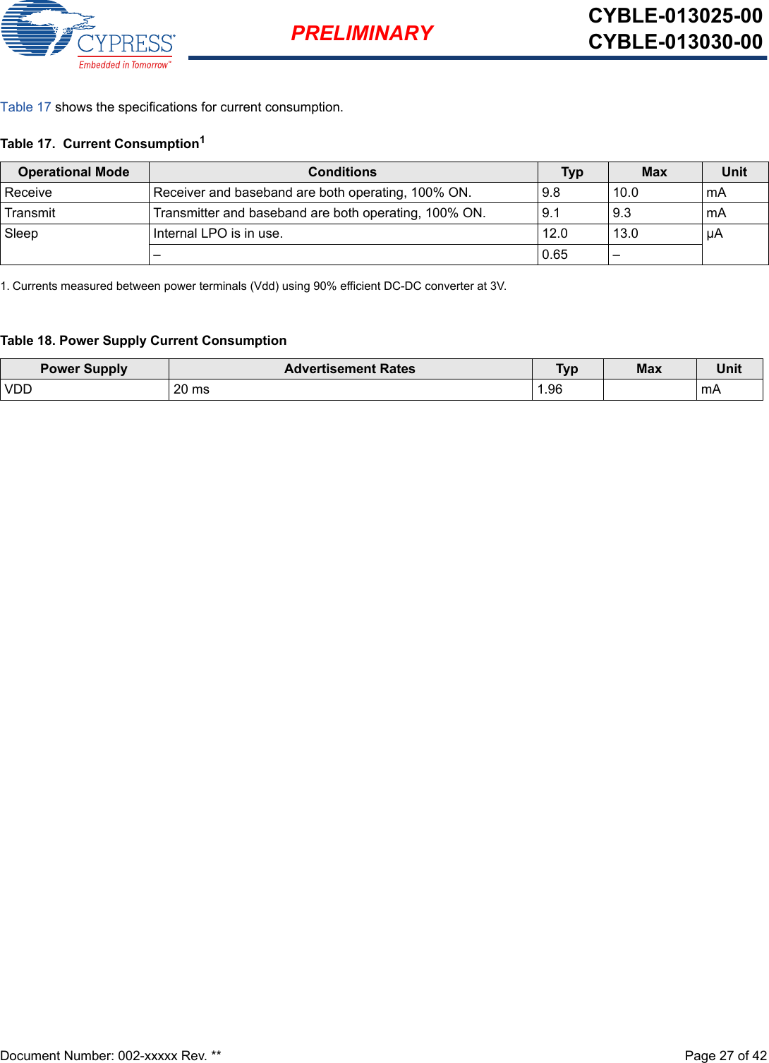
![PRELIMINARYCYBLE-013025-00CYBLE-013030-00EZ-BLE™ WICED ModuleCypress Semiconductor Corporation • 198 Champion Court • San Jose,CA 95134-1709 • 408-943-2600Document Number: 002-xxxxx Rev. ** Revised April 10, 2017General DescriptionThe CYBLE-0130XX-00 is a fully integrated Bluetooth LowEnergy (BLE) wireless module solution. The CYBLE-0130XX-00includes onboard crystal oscillator, passive components, flashmemory, and the Cypress CYW20737 silicon device. Refer to theCYW20737 datasheet for additional details on the capabilities ofthe silicon device used in this module. The CYBLE-0130XX-00 supports a number of peripheralfunctions (ADC and PWM), as well as UART serialcommunication. The CYBLE-0130XX-00 includes a royalty-freeBLE stack compatible with Bluetooth 4.1 in a 14.5 × 19.2 ×2.25mm package.The CYBLE-013025-00 includes 128KB of onboard flashmemory and is designed to allow for self-sufficient opperation.The CYBLE-013030-00 does not contain onboard flash,providing maximum cost optimization and allowing for hostedcontrol or application RAM upload, or interface to external flashon the host board. The CYBLE-0130XX-00 is fully certified by Bluetooth SIG istargeted at applications requiring cost optimized BLE wirelessconnectivity. The CYBLE-0130XX-00 is footprint compatible[1]with the CYBLE-x120xx-00 module family. Module DescriptionnModule size: 14.52 mm × 19.20 mm × 2.25 mm nBluetooth LE 4.1 single-mode modulepQDID: TBDpDeclaration ID: TBDnCertified to FCC, IC, MIC, and CE regulationsnCastelated solder pad connections for ease-of-usen128-KB flash memory, 60-KB SRAM memorynUp to 14 GPIOs configurable as open drain high/low, pull-up/pull-down, HI-Z analog, HI-Z digital, or strong outputnIndustrial temperature range: –30 °C to +85 °CnCortex-M3 32-bit processor nWatchdog timer with dedicated internal low-speed oscillatornSupports A4WP wireless chargingnSupports fRSA encryption/decryption and key exchange mechanisms (up to 4 kbit)nSupports NFC tag-based “tap-to-pair”nSupports IR learning with built-in IR modulatorPower ConsumptionnMaximum TX output power: +4.0 dbmnRX Receive Sensitivity: –94 dbmnReceived signal strength indicator (RSSI) with 1-dB resolutionnTX current consumption: 9.1 mA nRX current consumption: 9.8 mA nCypress CYW20737 silicon low power mode supportpSleep: 12 uA typicalpDeep Sleep: TBD Functional Capabilitiesn10-bit auxiliary ADC with nine analog channelsnSerial Communications interface (compatible with Philips® I2C slaves)nFour dedicated PWM blocks nBLE protocol stack supporting generic access profile (GAP) Central, Peripheral, Observer, or Broadcaster rolesnProgrammable output power controlBenefitsCYBLE-0130XX-00 provides all necessary components requiredto operate BLE communication standards. nProven hardware design ready to usenCost optimized for applications without space constraintsnNon-volatile memory for complex application developmentnOver-the-air update capable for in-field updatesnBluetooth SIG qualified with QDID and Declaration ID nFully certified module eliminates the time needed for design, development and certification processesnWICED™ SMART provides an easy-to-use integrated design environment (IDE) to configure, develop, and program a BLE applicationNotes1. CYBLE-0130XX-00 global connections (Power, Ground, XRES, etc) are pad compatible with the CYBLE-x120xx-00 family of modules. Available GPIO and functions may not be 100% compatible with your design. A review of the pad location and function within your design should be complete to determine if the CYBLE-0130XX-00 is completely pad-compatible to the CYBLE-x120xx-00 modules.](https://usermanual.wiki/Cypress-Semiconductor/3025/User-Guide-3375688-Page-1.png)
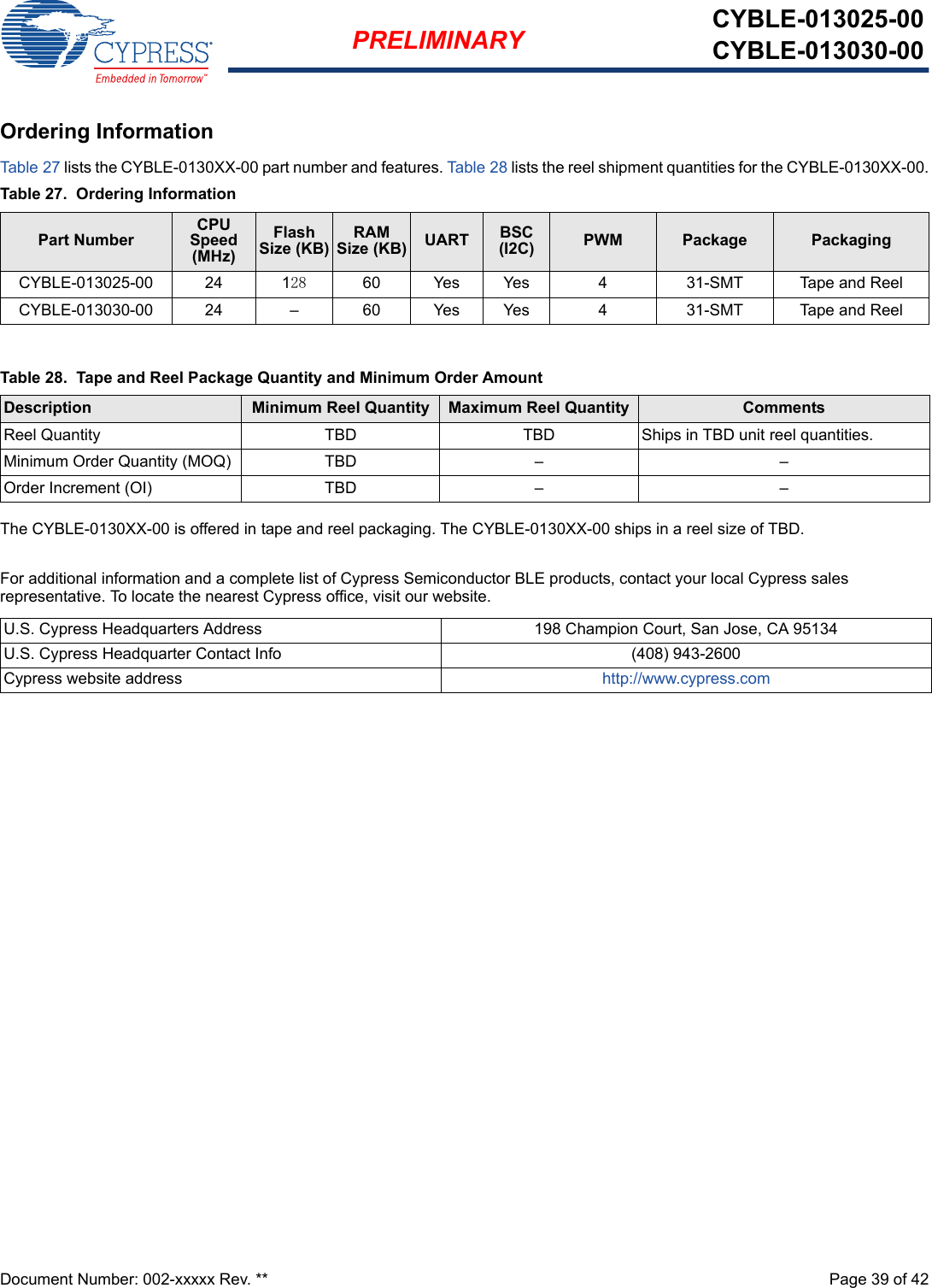
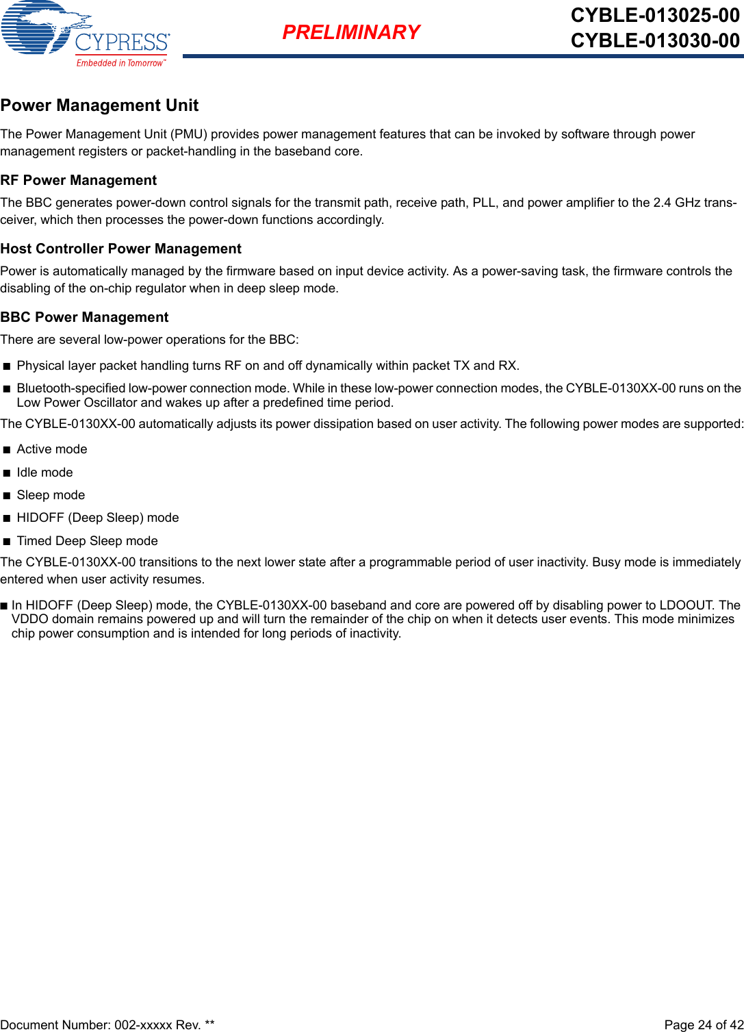
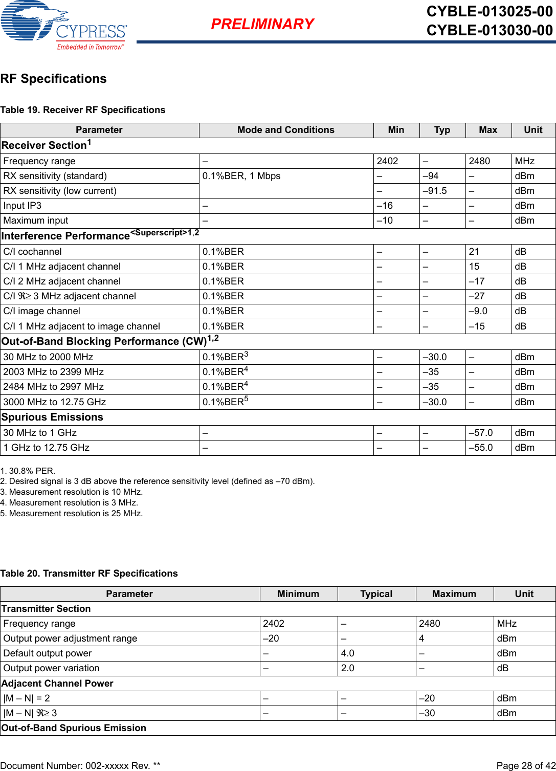
![Document Number: 002-xxxxx Rev. ** Page 14 of 42PRELIMINARY CYBLE-013025-00CYBLE-013030-00Bluetooth Low Energy ProfilesThe CYBLE-0130XX-00 supports Bluetooth low energy, including the following profiles that are supported[4] in ROM:nBattery statusnBlood pressure monitornFind menHeart rate monitornProximitynThermometernWeight scalenTimenAlliance for Wireless Power (A4WP) wireless chargingnAutomation profilenSupport for secure OTAThe following additional profiles can be supported[4] from RAM:nBlood glucose monitornTemperature alarmnLocationnCustom profileTest Mode SupportThe CYBLE-0130XX-00 fully supports Bluetooth Test mode, as described in the Bluetooth low energy specification.Infrared ModulatorThe CYBLE-0130XX-00 includes hardware support for infrared TX. The hardware can transmit both modulated and unmodulated waveforms. For modulated waveforms, hardware inserts the desired carrier frequency into all IR transmissions. IR TX can be sourced from firmware-supplied descriptors, a programmable bit, or the peripheral UART transmitter. If descriptors are used, they include IR on/off state and the duration between 1~32767 µsec. The CYBLE-0130XX-00 IR TX firmware driver inserts this information in a hardware FIFO and makes sure that all descriptors are played out without a glitch due to underrun (see Figure 9) . Notes4. Full qualification and use of these profiles may require FW updates from Cypress. Some of these profiles are under development/approval at the Bluetooth SIG and conformity with the final approved version is pending. Contact your local representative for updates and the latest list of profiles.](https://usermanual.wiki/Cypress-Semiconductor/3025/User-Guide-3375688-Page-14.png)
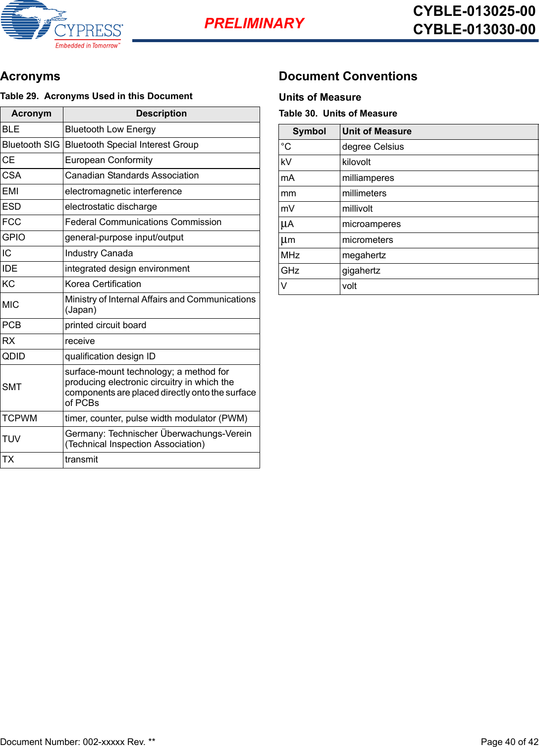
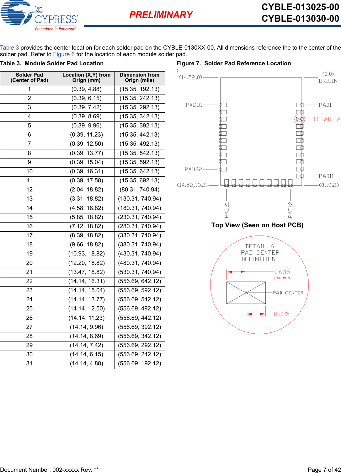
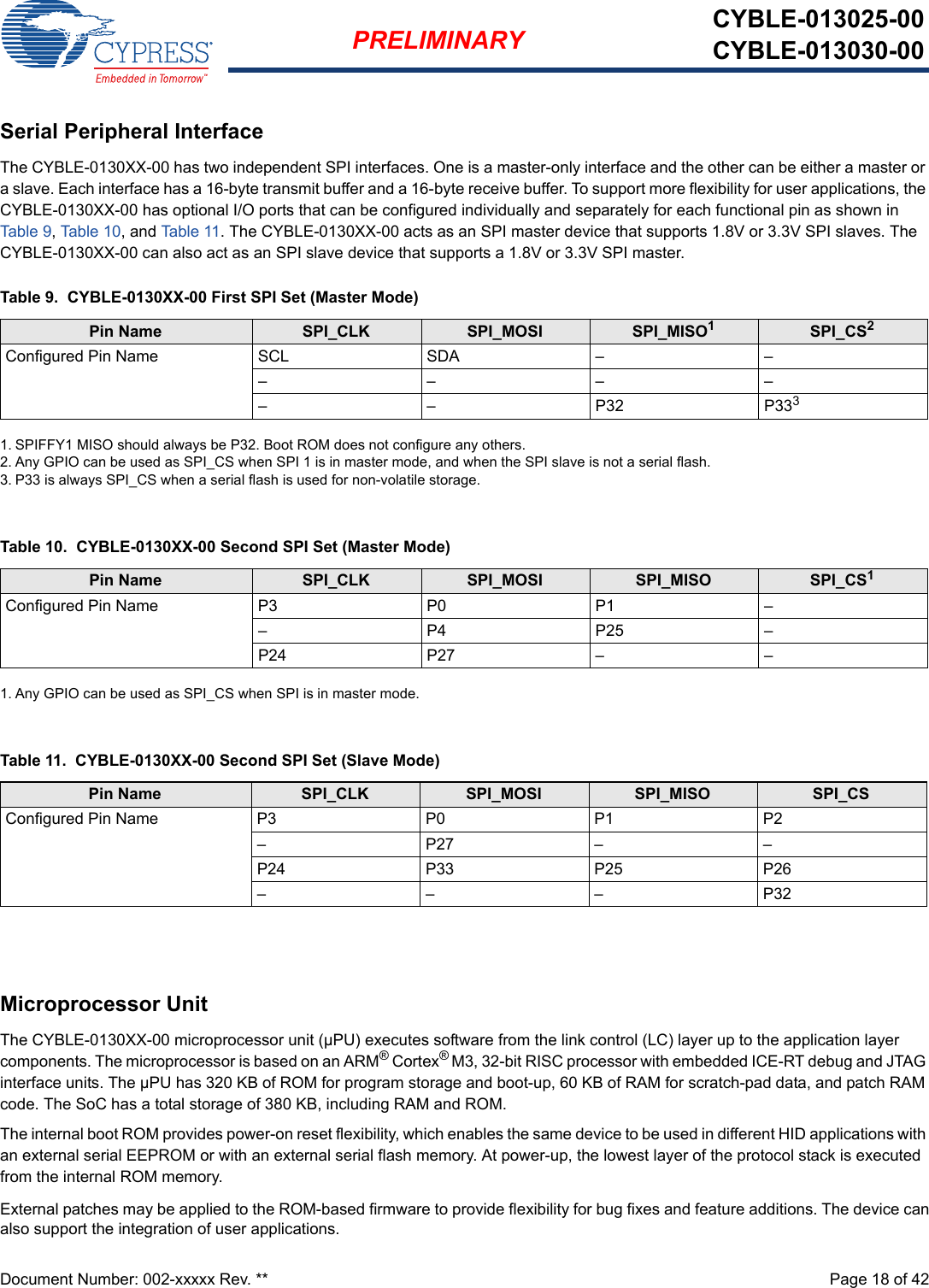
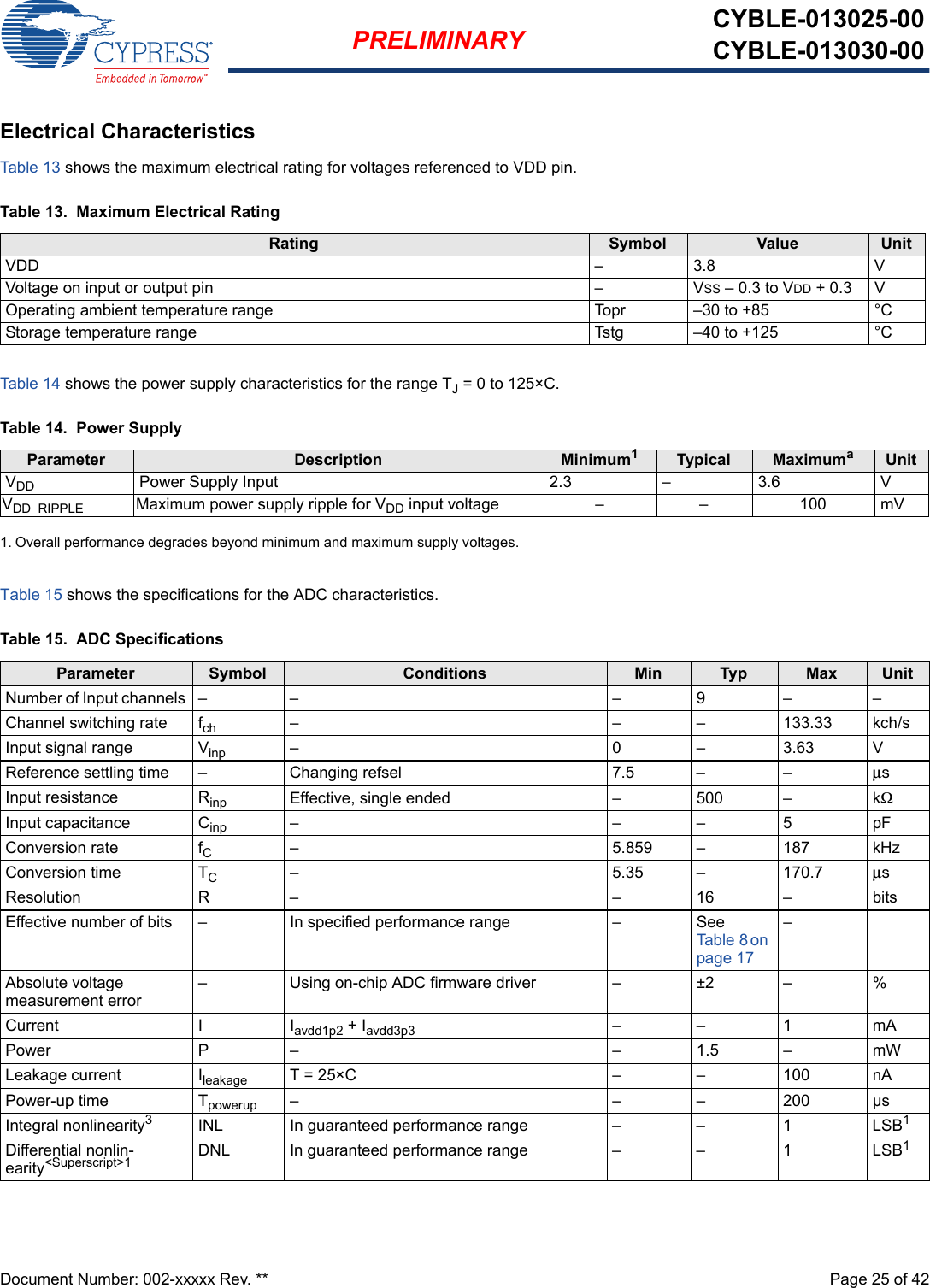
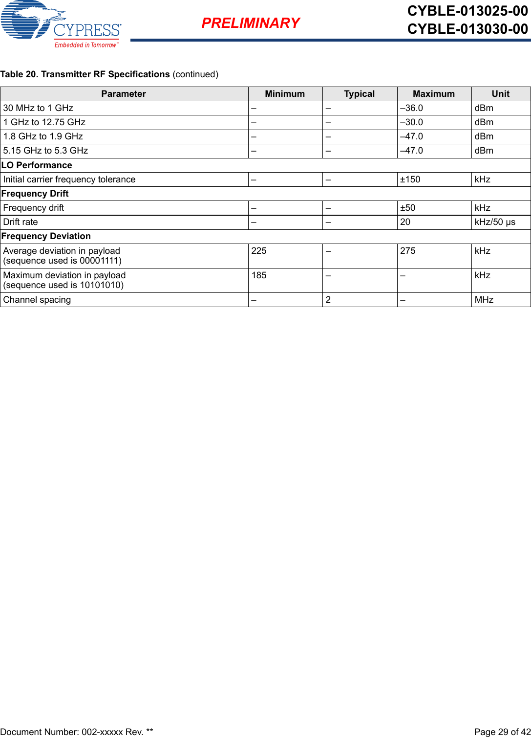
![Document Number: 002-xxxxx Rev. ** Page 17 of 42PRELIMINARY CYBLE-013025-00CYBLE-013030-00ADC PortThe CYBLE-0130XX-00 contains a 16-bit ADC (effective number of bits is 10).Additionally:nThere are 9 analog input channels in the 32-pin packagenThe following GPIOs can be used as ADC inputs: pP0pP1pP8/P33 (select only one)pP11 on P11/P27 pinpP12 on P12/28 pinpP13/P28 (select only one)pP14/P38 (select only one)pP15pP32nThe conversion time is 10 us.nThere is a built-in reference with supply- or bandgap-based reference modes.nThe maximum conversion rate is 187 kHz.nThere is a rail-to-rail input swing.The ADC consists of an analog ADC core that performs the actual analog-to-digital conversion and digital hardware that processes the output of the ADC core into valid ADC output samples. Directed by the firmware, the digital hardware also controls the input multiplexers that select the ADC input signal Vinp and the ADC reference signals Vref.The ADC input range is selectable by firmware control:nWhen an input range of 0~3.6V is used, the input impedance is 3 MW.nWhen an input range of 0~2.4V is used, the input impedance is 1.84 MW.nWhen an input range of 0~1.2V is used, the input impedance is 680 kW.ADC modes are defined in Ta b l e 8.Table 8. ADC ModesMode ENOB (Typical) Maximum Sampling Rate (kHz) Latency[5] (u?s)0 13 5.859 1711 12.6 11.7 85212 46.875 213 11.5 93.75 11410 187 55. Settling time after switching channels. .](https://usermanual.wiki/Cypress-Semiconductor/3025/User-Guide-3375688-Page-17.png)
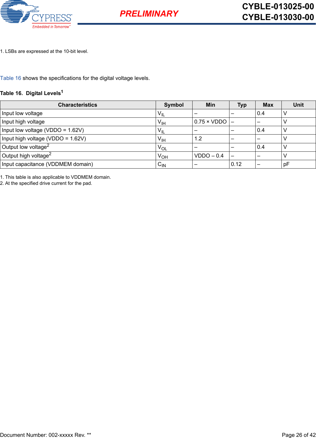
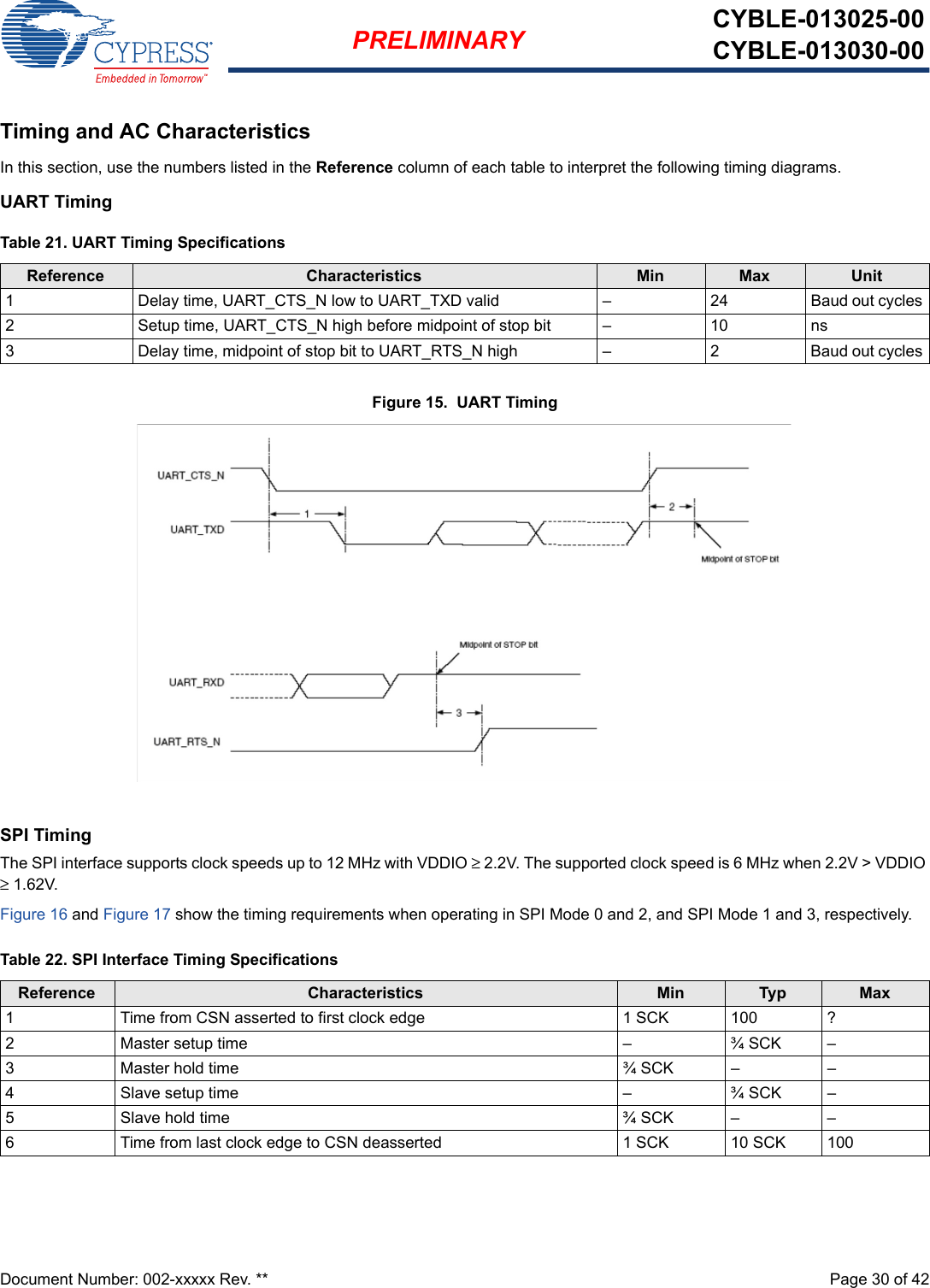
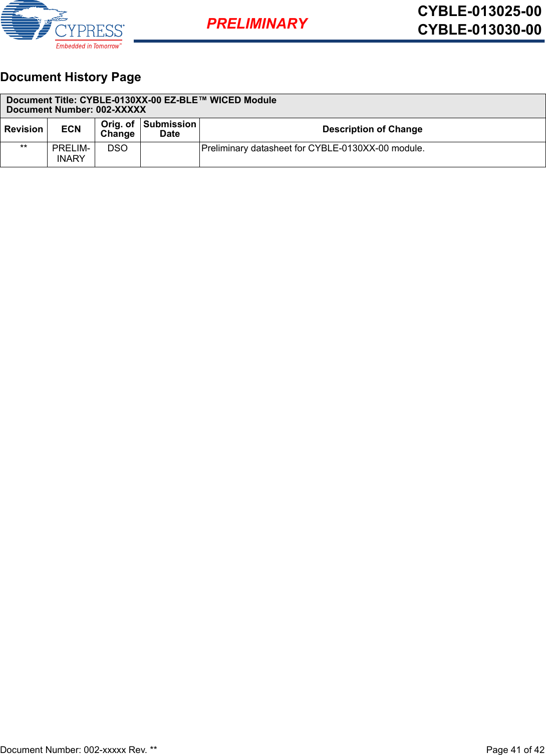
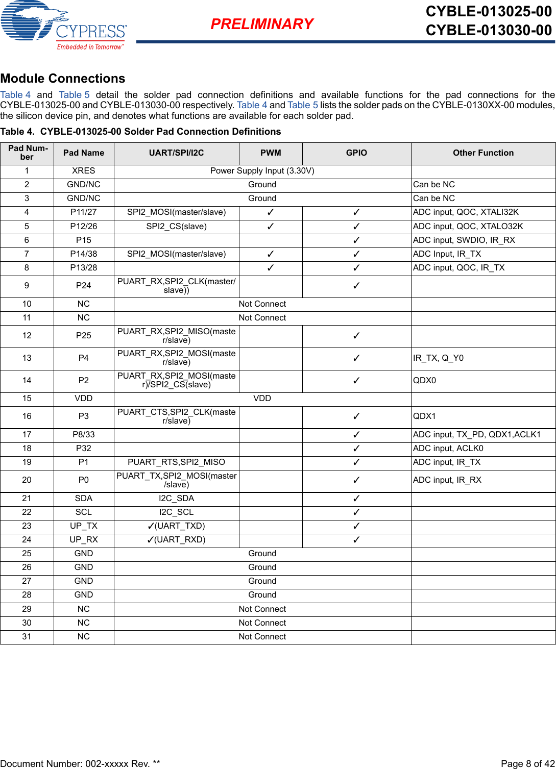
![Document Number: 002-xxxxx Rev. ** Page 33 of 42PRELIMINARY CYBLE-013025-00CYBLE-013030-00Environmental SpecificationsEnvironmental ComplianceThis Cypress BLE module is produced in compliance with the Restriction of Hazardous Substances (RoHS) and Halogen-Free (HF)directives. The Cypress module and components used to produce this module are RoHS and HF compliant.RF CertificationThe CYBLE-0130XX-00 module will be certified under the following RF certification standards at production release.nFCC: WAP3025nCEnIC: 7922A-3025nMIC: TBDSafety CertificationThe CYBLE-0130XX-00 module complies with the following safety regulations:nUnderwriters Laboratories, Inc. (UL): Filing E331901nCSAnTUVEnvironmental ConditionsTab l e 24 describes the operating and storage conditions for the Cypress BLE module.ESD and EMI ProtectionExposed components require special attention to ESD and electromagnetic interference (EMI).A grounded conductive layer inside the device enclosure is suggested for EMI and ESD performance. Any openings in the enclosurenear the module should be surrounded by a grounded conductive layer to provide ESD protection and a low-impedance path to ground. Device Handling: Proper ESD protocol must be followed in manufacturing to ensure component reliability.Table 24. Environmental Conditions for CYBLE-0130XX-00Description Minimum Specification Maximum SpecificationOperating temperature −30 °C 85 °COperating humidity (relative, non-condensation) 5% 85%Thermal ramp rate – 3 °C/minuteStorage temperature –40 °C 85 °CStorage temperature and humidity – 85 °C at 85%ESD: Module integrated into system Components[6] –15 kV Air2.0 kV ContactNote6. This does not apply to the RF pins (ANT).](https://usermanual.wiki/Cypress-Semiconductor/3025/User-Guide-3375688-Page-33.png)