Cypress Semiconductor 3025 Bluetooth Module User Manual CYBT 013033 01 EZ BT Module
Cypress Semiconductor Bluetooth Module CYBT 013033 01 EZ BT Module
User Manual

PRELIMINARY
CYBLE-013025-00
CYBLE-013030-00
EZ-BLE™ WICED Module
Cypress Semiconductor Corporation • 198 Champion Court • San Jose,CA 95134-1709 • 408-943-2600
Document Number: 002-xxxxx Rev. ** Revised April 10, 2017
General Description
The CYBLE-0130XX-00 is a fully integrated Bluetooth Low
Energy (BLE) wireless module solution. The CYBLE-0130XX-00
includes onboard crystal oscillator, passive components, flash
memory, and the Cypress CYW20737 silicon device. Refer to the
CYW20737 datasheet for additional details on the capabilities of
the silicon device used in this module.
The CYBLE-0130XX-00 supports a number of peripheral
functions (ADC and PWM), as well as UART serial
communication. The CYBLE-0130XX-00 includes a royalty-free
BLE stack compatible with Bluetooth 4.1 in a 14.5 × 19.2 ×
2.25mm package.
The CYBLE-013025-00 includes 128KB of onboard flash
memory and is designed to allow for self-sufficient opperation.
The CYBLE-013030-00 does not contain onboard flash,
providing maximum cost optimization and allowing for hosted
control or application RAM upload, or interface to external flash
on the host board.
The CYBLE-0130XX-00 is fully certified by Bluetooth SIG is
targeted at applications requiring cost optimized BLE wireless
connectivity. The CYBLE-0130XX-00 is footprint compatible[1]
with the CYBLE-x120xx-00 module family.
Module Description
nModule size: 14.52 mm × 19.20 mm × 2.25 mm
nBluetooth LE 4.1 single-mode module
pQDID: TBD
pDeclaration ID: TBD
nCertified to FCC, IC, MIC, and CE regulations
nCastelated solder pad connections for ease-of-use
n128-KB flash memory, 60-KB SRAM memory
nUp to 14 GPIOs configurable as open drain high/low,
pull-up/pull-down, HI-Z analog, HI-Z digital, or strong output
nIndustrial temperature range: –30 °C to +85 °C
nCortex-M3 32-bit processor
nWatchdog timer with dedicated internal low-speed oscillator
nSupports A4WP wireless charging
nSupports fRSA encryption/decryption and key exchange
mechanisms (up to 4 kbit)
nSupports NFC tag-based “tap-to-pair”
nSupports IR learning with built-in IR modulator
Power Consumption
nMaximum TX output power: +4.0 dbm
nRX Receive Sensitivity: –94 dbm
nReceived signal strength indicator (RSSI) with 1-dB resolution
nTX current consumption: 9.1 mA
nRX current consumption: 9.8 mA
nCypress CYW20737 silicon low power mode support
pSleep: 12 uA typical
pDeep Sleep: TBD
Functional Capabilities
n10-bit auxiliary ADC with nine analog channels
nSerial Communications interface (compatible with Philips® I2C
slaves)
nFour dedicated PWM blocks
nBLE protocol stack supporting generic access profile (GAP)
Central, Peripheral, Observer, or Broadcaster roles
nProgrammable output power control
Benefits
CYBLE-0130XX-00 provides all necessary components required
to operate BLE communication standards.
nProven hardware design ready to use
nCost optimized for applications without space constraints
nNon-volatile memory for complex application development
nOver-the-air update capable for in-field updates
nBluetooth SIG qualified with QDID and Declaration ID
nFully certified module eliminates the time needed for design,
development and certification processes
nWICED™ SMART provides an easy-to-use integrated design
environment (IDE) to configure, develop, and program a BLE
application
Notes
1. CYBLE-0130XX-00 global connections (Power, Ground, XRES, etc) are pad compatible with the CYBLE-x120xx-00 family of modules. Available GPIO and functions
may not be 100% compatible with your design. A review of the pad location and function within your design should be complete to determine if the CYBLE-0130XX-00
is completely pad-compatible to the CYBLE-x120xx-00 modules.

Document Number: 002-xxxxx Rev. ** Page 2 of 42
PRELIMINARY CYBLE-013025-00
CYBLE-013030-00
Contents
Overview............................................................................ 3
Functional Block Diagram ........................................... 3
Module Description...................................................... 3
Pad Connection Interface ................................................ 5
Recommended Host PCB Layout ................................... 6
Module Connections ........................................................ 8
Connections and Optional External Components ..... 10
Power Connections (VDD) ........................................ 10
External Reset (XRES).............................................. 10
External Component Recommendation .................... 10
Critical Components List ........................................... 12
Antenna Design......................................................... 12
Bluetooth Baseband Core ............................................. 13
Infrared Modulator.......................................................... 14
Infrared Learning ............................................................ 15
Wireless Charging .......................................................... 16
Security ........................................................................... 16
Support for NFC Tag Based Pairing ............................. 16
Bluetooth Smart Audio .................................................. 16
ADC Port.......................................................................... 17
Serial Peripheral Interface ............................................. 18
Microprocessor Unit....................................................... 18
Internal Reset ............................................................ 19
External Reset (XRES).............................................. 19
Integrated Radio Transceiver ........................................ 20
Transmitter Path........................................................ 20
Digital Modulator ....................................................... 20
Power Amplifier ......................................................... 20
Receiver Path............................................................ 20
Digital Demodulator and Bit Synchronizer................. 20
Receiver Signal Strength Indicator............................ 20
Local Oscillator.......................................................... 20
Calibration ................................................................. 20
Internal LDO Regulator ............................................. 20
Peripheral Transport Unit .............................................. 21
Broadcom Serial Communications Interface............. 21
Peripheral Block ........................................................ 21
GPIO Port ........................................................................ 22
PWM................................................................................. 23
Power Management Unit................................................ 24
RF Power Management ............................................ 24
Host Controller Power Management ......................... 24
BBC Power Management.......................................... 24
Electrical Characteristics............................................... 25
RF Specifications ........................................................... 28
Timing and AC Characteristics ..................................... 30
UART Timing............................................................. 30
SPI Timing................................................................. 30
BSC Interface Timing ................................................ 31
Environmental Specifications ....................................... 33
Environmental Compliance ....................................... 33
RF Certification.......................................................... 33
Safety Certification .................................................... 33
Environmental Conditions ......................................... 33
ESD and EMI Protection ........................................... 33
Regulatory Information.................................................. 34
FCC........................................................................... 34
Industry Canada (IC) Certification............................. 35
European R&TTE Declaration of Conformity ............ 35
MIC Japan................................................................. 36
Packaging........................................................................ 37
Ordering Information...................................................... 39
Acronyms........................................................................ 40
Document Conventions ................................................. 40
Units of Measure ....................................................... 40
Document History Page................................................. 41
Sales, Solutions, and Legal Information ...................... 42
Worldwide Sales and Design Support....................... 42
Products .................................................................... 42
PSoC® Solutions ...................................................... 42
Cypress Developer Community................................. 42
Technical Support ..................................................... 42
Document Number: 002-xxxxx Rev. ** Page 3 of 42
PRELIMINARY CYBLE-013025-00
CYBLE-013030-00
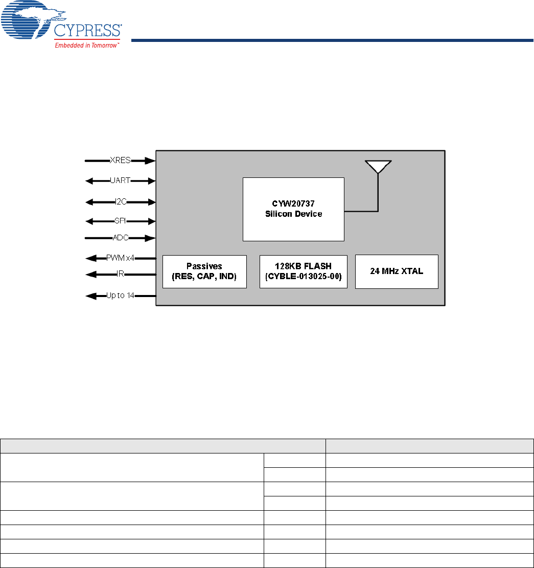
Overview
Functional Block Diagram
Figure 1 illustrates the CYBLE-0130XX-00 functional block diagram.
Figure 1. Functional Block Diagram
Module Description
The CYBLE-0130XX-00 module is a complete module designed to be soldered to the applications main board.
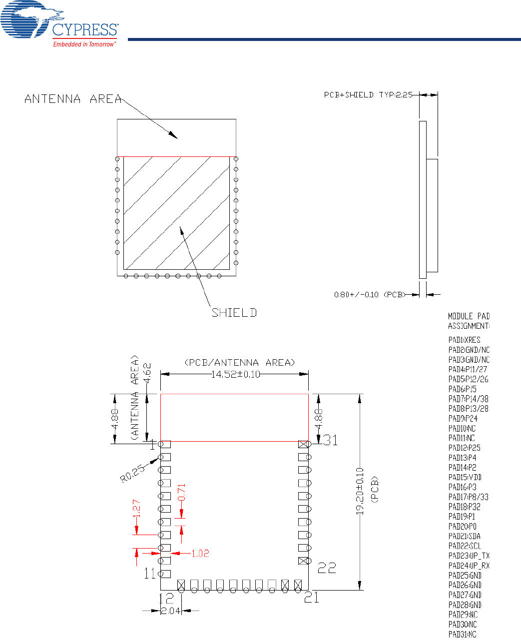
Module Dimensions and Drawing
Cypress reserves the right to select components from various vendors to achieve the Bluetooth module functionality. Such selections
will still guarantee that all mechanical specifications and module certifications are maintained. Designs should be held within the
physical dimensions shown in the mechanical drawings in Figure 2 on page 4. All dimensions are in millimeters (mm).
Table 1. Module Design Dimensions
See Figure 2 for the mechanical reference drawing for CYBLE-0130XX-00.
Dimension Item Specification
Module dimensions Length (X) 14.52 ± 0.10 mm
Width (Y) 19.50 ± 0.10 mm
Antenna connection location dimensions Length (X) 14.52 mm
Width (Y) 4.80 mm
PCB thickness Height (H) 0.80 ± 0.10 mm
Shield height Height (H) 1.45 mm typical
Maximum component height Height (H) 1.45 mm typical
Total module thickness (bottom of module to highest component) Height (H) 2.25 mm typical
Document Number: 002-xxxxx Rev. ** Page 4 of 42
PRELIMINARY CYBLE-013025-00
CYBLE-013030-00
Figure 2. Module Mechanical Drawing
Bottom View (Seen from Bottom)
Side View
Top View (See from Top)
Notes
2. No metal should be located beneath or above the antenna area. Only bare PCB material should be located beneath the antenna area. For more information on
recommended host PCB layout, see “Recommended Host PCB Layout” on page 6.
3. The CYBLE-0130XX-00 includes castellated pad connections, denoted as the circular openings at the pad location above.
Document Number: 002-xxxxx Rev. ** Page 5 of 42
PRELIMINARY CYBLE-013025-00
CYBLE-013030-00
Pad Connection Interface
As shown in the bottom view of Figure 2 on page 4, the CYBLE-0130XX-00 connects to the host board via solder pads on the backside
of the module. Table 2 and Figure 3 detail the solder pad length, width, and pitch dimensions of the CYBLE-0130XX-00 module.
Figure 3. Solder Pad Dimensions (Seen from Bottom)
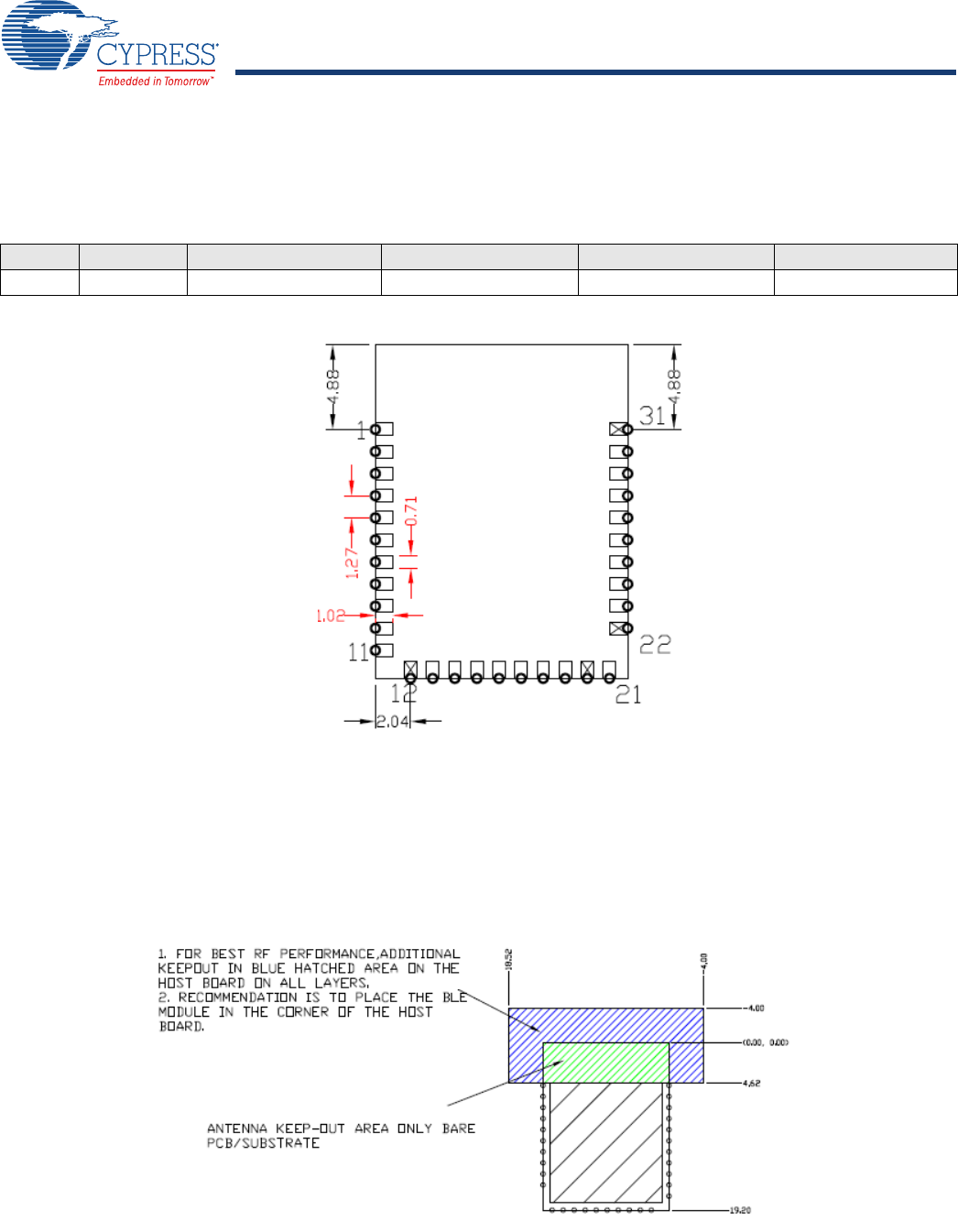
To maximize RF performance, the host layout should follow these recommendations:
1. The ideal placement of the Cypress BLE module is in a corner of the host board with the trace antenna located at the far corner.
This placement minimizes the additional recommended keep out area stated in item 2. Please refer to AN96841 for module
placement best practices.
2. To maximize RF performance, the area immediately around the Cypress BLE module trace antenna should contain an additional
keep out area, where no grounding or signal trace are contained. The keep out area applies to all layers of the host board. The
recommended dimensions of the host PCB keep out area are shown in Figure 4 (dimensions are in mm).
Figure 4. Recommended Host PCB Keep Out Area Around the CYBLE-0130XX-00 Antenna
Table 2. Connection Description
Name Connections Connection Type Pad Length Dimension Pad Width Dimension Pad Pitch
SP 31 Solder Pads 1.02 mm 0.71 mm 1.27 mm
Document Number: 002-xxxxx Rev. ** Page 6 of 42
PRELIMINARY CYBLE-013025-00
CYBLE-013030-00
Recommended Host PCB Layout
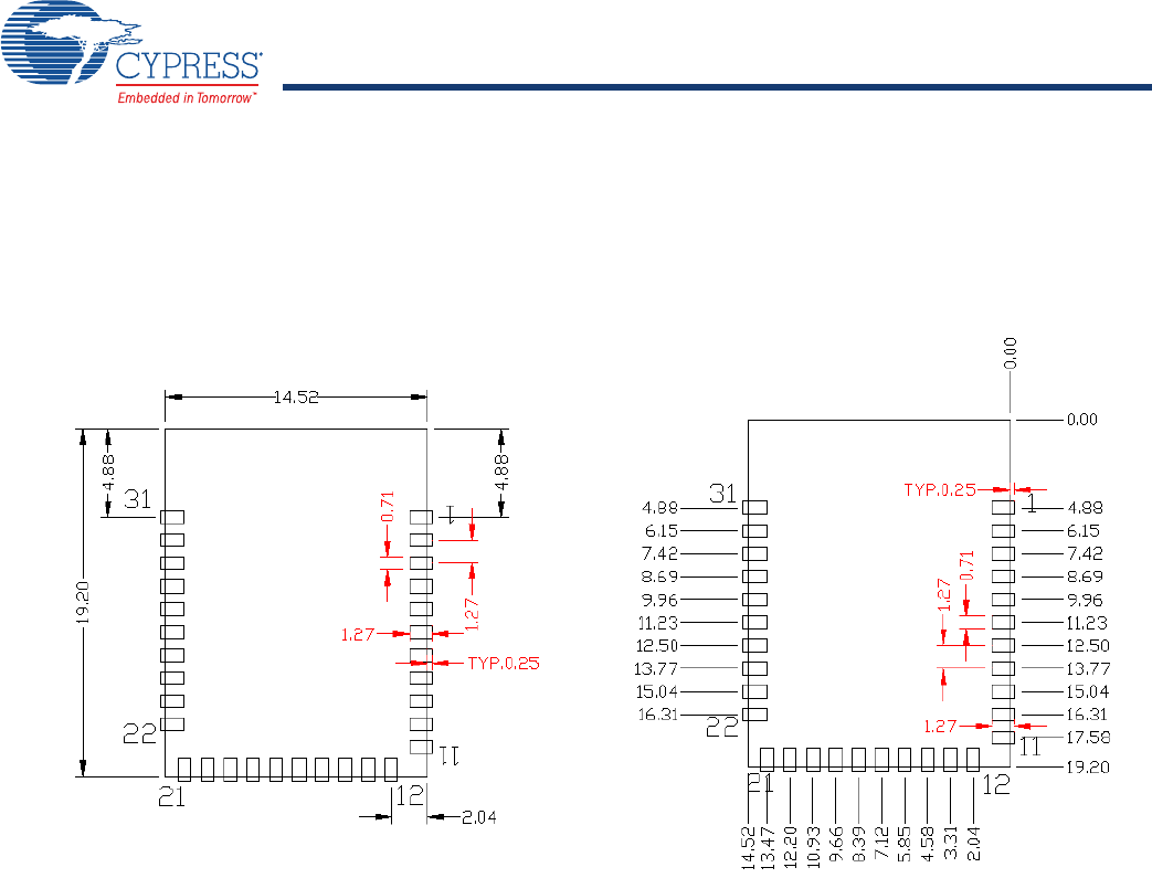
Figure 5, Figure 6, Figure 7, and Table 3 provide details that can be used for the recommended host PCB layout pattern for the
CYBLE-0130XX-00. Dimensions are in millimeters unless otherwise noted. Pad length of 1.27 mm (0.635 mm from center of the pad
on either side) shown in Figure 7 is the minimum recommended host pad length. The host PCB layout pattern can be completed using
either Figure 5, Figure 6, or Figure 7. It is not necessary to use all figures to complete the host PCB layout pattern.
Figure 5. CYBLE-0130XX-00 Host Layout (Dimensioned) Figure 6. CYBLE-0130XX-00 Host Layout (Relative to Origin)
Top View (Seen on Host PCB)
Top View (Seen on Host PCB)
Document Number: 002-xxxxx Rev. ** Page 7 of 42
PRELIMINARY CYBLE-013025-00
CYBLE-013030-00
Tab l e 3 provides the center location for each solder pad on the CYBLE-0130XX-00. All dimensions reference the to the center of the
solder pad. Refer to Figure 6 for the location of each module solder pad.
Table 3. Module Solder Pad Location Figure 7. Solder Pad Reference Location
Solder Pad
(Center of Pad)
Location (X,Y) from
Orign (mm)
Dimension from
Orign (mils)
1 (0.39, 4.88) (15.35, 192.13)
2 (0.39, 6.15) (15.35, 242.13)
3 (0.39, 7.42) (15.35, 292.13)
4 (0.39, 8.69) (15.35, 342.13)
5 (0.39, 9.96) (15.35, 392.13)
6 (0.39, 11.23) (15.35, 442.13)
7 (0.39, 12.50) (15.35, 492.13)
8 (0.39, 13.77) (15.35, 542.13)
9 (0.39, 15.04) (15.35, 592.13)
10 (0.39, 16.31) (15.35, 642.13)
11 (0.39, 17.58) (15.35, 692.13)
12 (2.04, 18.82) (80.31, 740.94)
13 (3.31, 18.82) (130.31, 740.94)
14 (4.58, 18.82) (180.31, 740.94)
15 (5.85, 18.82) (230.31, 740.94)
16 (7.12, 18.82) (280.31, 740.94)
17 (8.39, 18.82) (330.31, 740.94)
18 (9.66, 18.82) (380.31, 740.94)
19 (10.93, 18.82) (430.31, 740.94)
20 (12.20, 18.82) (480.31, 740.94)
21 (13.47, 18.82) (530.31, 740.94)
22 (14.14, 16.31) (556.69, 642.12)
23 (14.14, 15.04) (556.69, 592.12)
24 (14.14, 13.77) (556.69, 542.12)
25 (14.14, 12.50) (556.69, 492.12)
26 (14.14, 11.23) (556.69, 442.12)
27 (14.14, 9.96) (556.69, 392.12)
28 (14.14, 8.69) (556.69, 342.12)
29 (14.14, 7.42) (556.69, 292.12)
30 (14.14, 6.15) (556.69, 242.12)
31 (14.14, 4.88) (556.69, 192.12)
Top View (Seen on Host PCB)

Document Number: 002-xxxxx Rev. ** Page 8 of 42
PRELIMINARY CYBLE-013025-00
CYBLE-013030-00
Module Connections
Tab l e 4 and Table 5 detail the solder pad connection definitions and available functions for the pad connections for the
CYBLE-013025-00 and CYBLE-013030-00 respectively. Table 4 and Ta ble 5 lists the solder pads on the CYBLE-0130XX-00 modules,
the silicon device pin, and denotes what functions are available for each solder pad.
Table 4. CYBLE-013025-00 Solder Pad Connection Definitions
Pad Num-
ber Pad Name UART/SPI/I2C PWM GPIO Other Function
1 XRES Power Supply Input (3.30V)
2 GND/NC Ground Can be NC
3 GND/NC Ground Can be NC
4 P11/27 SPI2_MOSI(master/slave) 33ADC input, QOC, XTALI32K
5 P12/26 SPI2_CS(slave) 33ADC input, QOC, XTALO32K
6P15 3ADC input, SWDIO, IR_RX
7 P14/38 SPI2_MOSI(master/slave) 33ADC Input, IR_TX
8P13/28 33ADC input, QOC, IR_TX
9P24
PUART_RX,SPI2_CLK(master/
slave)) 3
10 NC Not Connect
11 NC Not Connect
12 P25 PUART_RX,SPI2_MISO(maste
r/slave) 3
13 P4 PUART_RX,SPI2_MOSI(maste
r/slave) 3IR_TX, Q_Y0
14 P2 PUART_RX,SPI2_MOSI(maste
r)/SPI2_CS(slave) 3QDX0
15 VDD VDD
16 P3 PUART_CTS,SPI2_CLK(maste
r/slave) 3QDX1
17 P8/33 3ADC input, TX_PD, QDX1,ACLK1
18 P32 3ADC input, ACLK0
19 P1 PUART_RTS,SPI2_MISO 3ADC input, IR_TX
20 P0 PUART_TX,SPI2_MOSI(master
/slave) 3ADC input, IR_RX
21 SDA I2C_SDA 3
22 SCL I2C_SCL 3
23 UP_TX 3(UART_TXD) 3
24 UP_RX 3(UART_RXD) 3
25 GND Ground
26 GND Ground
27 GND Ground
28 GND Ground
29 NC Not Connect
30 NC Not Connect
31 NC Not Connect
Document Number: 002-xxxxx Rev. ** Page 9 of 42
PRELIMINARY CYBLE-013025-00
CYBLE-013030-00
Table 5. CYBLE-013030-00 Solder Pad Connection Definitions
Pad Num-
ber Pad Name UART/SPI/I2C PWM GPIO Other Function
1 XRES Power Supply Input (3.30V)
2 GND/NC Ground Can be NC
3 GND/NC Ground Can be NC
4 P11/27 SPI2_MOSI(master/slave) 33ADC input, QOC, XTALI32K
5 P12/26 SPI2_CS(slave) 33ADC input, QOC, XTALO32K
6P15 3ADC input, SWDIO, IR_RX
7 P14/38 SPI2_MOSI(master/slave) 33ADC Input, IR_TX
8P13/28 33ADC input, QOC, IR_TX
9P24
PUART_RX,SPI2_CLK(master/
slave)) 3
10 NC Not Connect
11 NC Not Connect
12 P25 PUART_RX,SPI2_MISO(maste
r/slave) 3
13 P4 PUART_RX,SPI2_MOSI(maste
r/slave) 3IR_TX, Q_Y0
14 P2 PUART_RX,SPI2_MOSI(maste
r)/SPI2_CS(slave) 3QDX0
15 VDD VDD
16 P3 PUART_CTS,SPI2_CLK(maste
r/slave) 3QDX1
17 P8/33 PUART_RX,SPI1_MOSI 3ADC input, TX_PD, QDX1,ACLK1
18 P32 PUART_TX,SPI1_MISO/CS 3ADC input, ACLK0
19 P1 PUART_RTS,SPI2_MISO 3ADC input, IR_TX
20 P0 PUART_TX,SPI2_MOSI(master
/slave) 3ADC input, IR_RX
21 SDA I2C_SDA 3
22 SCL I2C_SCL 3
23 UP_TX 3(UART_TXD) 3
24 UP_RX 3(UART_RXD) 3
25 GND Ground
26 GND Ground
27 GND Ground
28 GND Ground
29 NC Not Connect
30 NC Not Connect
31 NC Not Connect

Document Number: 002-xxxxx Rev. ** Page 10 of 42
PRELIMINARY CYBLE-013025-00
CYBLE-013030-00
Connections and Optional External Components
Power Connections (VDD)
The CYBLE-0130XX-00 contains one power supply connection, VDD.
VDD accepts a supply input range of 2.3V to 3.6 V. Table 14 provides this specification. The maximum power supply ripple for this
power connection is 100 mV, as shown in Table 14.
External Reset (XRES)
The CYBLE-0130XX-00 has an integrated power-on reset circuit which completely resets all circuits to a known power on state. This
action can also be driven by an external reset signal, which can be used to externally control the device, forcing it into a power-on
reset state. The XRES signal is an active-low signal, which is an input to the CYBLE-0130XX-00 module.
External Component Recommendation
Power Supply Circuitry
It is not required to place any power supply decoupling or noise reduction circuitry on the host PCB. If desired, an external ferrite bead
between the supply and the module connection can be included, but is not necessary. If used, the ferrite bead should be positioned
as close as possible to the module pin connection.
If used, the recommended ferrite bead value is 330Ω, 100 MHz. (Murata BLM21PG331SN1D).
Document Number: 002-xxxxx Rev. ** Page 12 of 42
PRELIMINARY CYBLE-013025-00
CYBLE-013030-00
Critical Components List
Tab l e 6 details the critical components used in the CYBLE-0130XX-00 module.
Table 6. Critical Component List
Antenna Design
Tab l e 7 details trace antenna used in the CYBLE-0130XX-00 module. For more information, see Table 7 .
Table 7. Trace Antenna Specifications
Component Reference Designator Description
Silicon U1 32-pin QFN BLE Silicon Device - CYW20737r
Silicon U2 8-pin TDF8N, 128KSerial Flash
Crystal Y1 24.000 MHz, 12PF
Item Description
Frequency Range 2400 – 2500 MHz
Peak Gain 0.5 dBi typical
Return Loss 10 dB minimum

Document Number: 002-xxxxx Rev. ** Page 13 of 42
PRELIMINARY CYBLE-013025-00
CYBLE-013030-00
Bluetooth Baseband Core
The Bluetooth Baseband Core (BBC) implements all of the time-critical functions required for high performance Bluetooth operation.
The BBC manages the buffering, segmentation, and data routing for all connections. It also buffers data that passes through it, han-
dles data flow control, schedules ACL TX/RX transactions, monitors Bluetooth slot usage, optimally segments and packages data
into baseband packets, manages connection status indicators, and composes and decodes HCI packets. In addition to these func-
tions, it independently handles HCI event types and HCI command types.
The following transmit and receive functions are also implemented in the BBC hardware to increase TX/RX data reliability and secu-
rity before sending over the air:
The following transmit and receive functions are also implemented in the BBC hardware to increase TX/RX data reliability and security
before sending over the air:
nReceive Functions: symbol timing recovery, data deframing, forward error correction (FEC), header error control (HEC), cyclic
redundancy check (CRC), data decryption, and data dewhitening.
nTransmit Functions: data framing, FEC generation, HEC generation, CRC generation, link key generation, data encryption, and data
whitening.
Frequency Hopping Generator
The frequency hopping sequence generator selects the correct hopping channel number depending on the link controller state,
Bluetooth clock, and device address.
E0 Encryption
The encryption key and the encryption engine are implemented using dedicated hardware to reduce software complexity and provide
minimal processor intervention.
Link Control Layer
The link control layer is part of the Bluetooth link control functions that are implemented in dedicated logic in the Link Control Unit
(LCU). This layer consists of the Command Controller, which takes software commands, and other controllers that are activated or
configured by the Command Controller to perform the link control tasks. Each task performs a different Bluetooth link controller state.
STANDBY and CONNECTION are the two major states. In addition, there are five substates: page, page scan, inquiry, and inquiry
scan.
Adaptive Frequency Hopping
The CYBLE-0130XX-00 gathers link quality statistics on a channel-by-channel basis to facilitate channel assessment and channel
map selection. The link quality is determined by using both RF and baseband signal processing to provide a more accurate frequency
hop map.

Document Number: 002-xxxxx Rev. ** Page 14 of 42
PRELIMINARY CYBLE-013025-00
CYBLE-013030-00
Bluetooth Low Energy Profiles
The CYBLE-0130XX-00 supports Bluetooth low energy, including the following profiles that are supported[4] in ROM:
nBattery status
nBlood pressure monitor
nFind me
nHeart rate monitor
nProximity
nThermometer
nWeight scale
nTime
nAlliance for Wireless Power (A4WP) wireless charging
nAutomation profile
nSupport for secure OTA
The following additional profiles can be supported[4] from RAM:
nBlood glucose monitor
nTemperature alarm
nLocation
nCustom profile
Test Mode Support
The CYBLE-0130XX-00 fully supports Bluetooth Test mode, as described in the Bluetooth low energy specification.
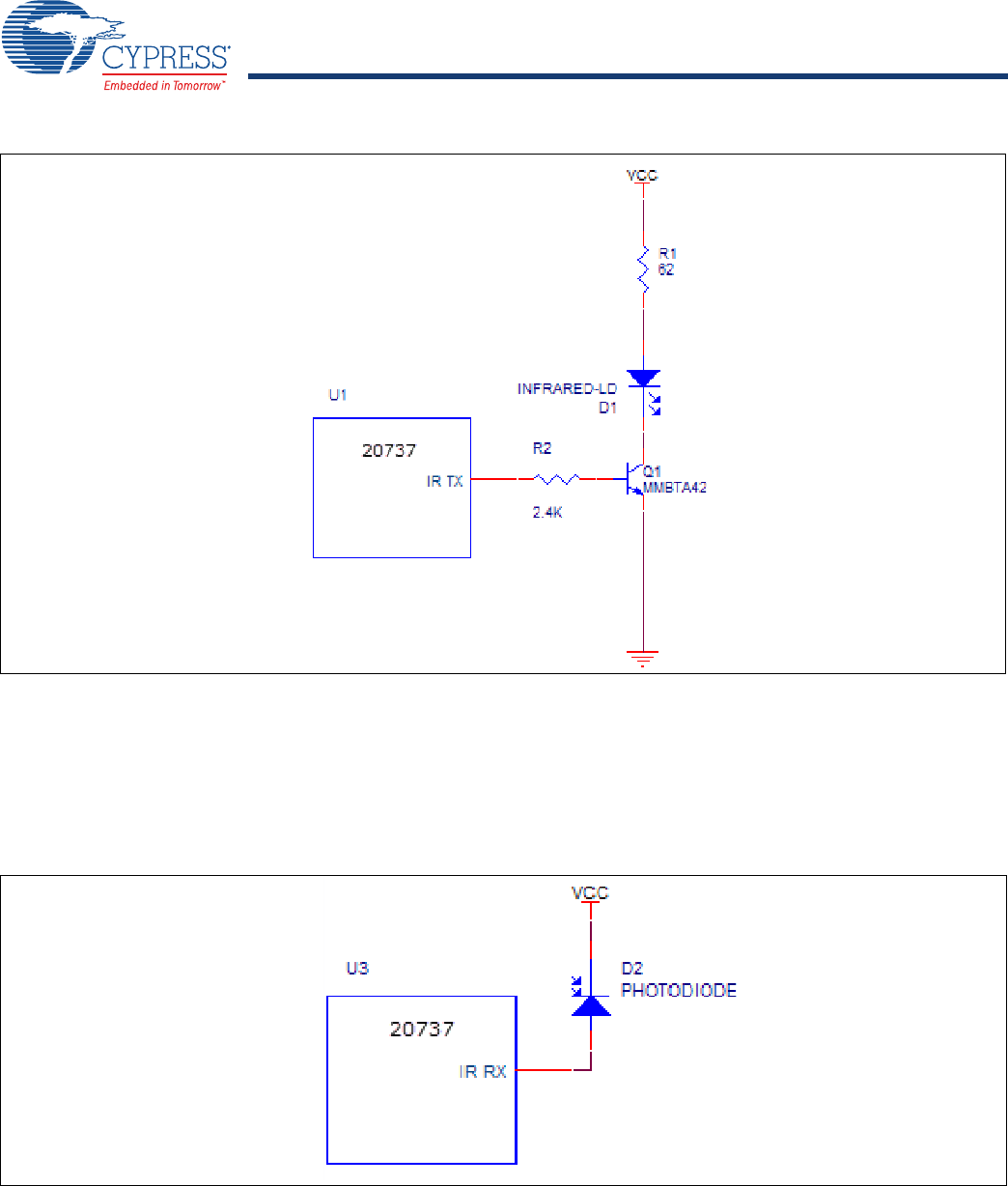
Infrared Modulator
The CYBLE-0130XX-00 includes hardware support for infrared TX. The hardware can transmit both modulated and unmodulated
waveforms. For modulated waveforms, hardware inserts the desired carrier frequency into all IR transmissions. IR TX can be sourced
from firmware-supplied descriptors, a programmable bit, or the peripheral UART transmitter.
If descriptors are used, they include IR on/off state and the duration between 1~32767 µsec. The CYBLE-0130XX-00 IR TX firmware
driver inserts this information in a hardware FIFO and makes sure that all descriptors are played out without a glitch due to underrun
(see Figure 9) .
Notes
4. Full qualification and use of these profiles may require FW updates from Cypress. Some of these profiles are under development/approval at the Bluetooth SIG and
conformity with the final approved version is pending. Contact your local representative for updates and the latest list of profiles.
Document Number: 002-xxxxx Rev. ** Page 15 of 42
PRELIMINARY CYBLE-013025-00
CYBLE-013030-00
Figure 9. Infrared TX
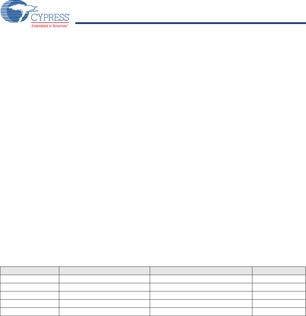
Infrared Learning
The CYBLE-0130XX-00 includes hardware support for infrared learning. The hardware can detect both modulated and unmodulated
signals. For modulated signals, the CYBLE-0130XX-00 can detect carrier frequencies between 10 kHz~500 kHz and the duration that
the signal is present or absent. The CYBLE-0130XX-00 firmware driver supports further analysis and compression of learned signal.
The learned signal can then be played back through the CYBLE-0130XX-00 IR TX subsystem (see Figure 10).
Figure 10. Infrared RX

Document Number: 002-xxxxx Rev. ** Page 16 of 42
PRELIMINARY CYBLE-013025-00
CYBLE-013030-00
Wireless Charging
The CYBLE-0130XX-00 includes support for wireless charging in hardware, software, and firmware. It supports the protocol for
implementing wireless charging solutions based on the specifications written by the Alliance for Wireless Power (A4WP).
The A4WP protocol is embedded in the CYBLE-0130XX-00. Hardware and firmware elements required for wireless charging are either
implemented in the CYBLE-0130XX-00 or can be obtained through a Cypress technical support representative.
An end-to-end charging solution comprises of the following:
nPower Transmitting Unit (PTU): The PTU transfers the power to the receiving unit. The receiving unit is any device (phone, wearable,
or other embedded device) that needs to be charged. The PTU is typically plugged into a power source such as a wall outlet. The
CYBLE-0130XX-00 includes the peripherals needed to implement and drive a reference charging circuit and otherwise requires
only a few external components. PTU reference designs based on the CYBLE-0130XX-00, including bills of material (BOMs), are
available through Cypress technical support. Depending on charging power requirements, a Power Management Unit (PMU) such
as the BCM8935X may be included in the design. However, most PTUs requiring < 5W will not need a PMU. The references designs
leverage ADCs, PWMs, and other internal peripherals to help drive the charging circuitry for energy transfer as well as provide
feedback for charging control. The application and algorithm that drive the reference designs are available on request.
nPower Receive Unit (PRU): The PRU receives energy from the PTU to charge the local device, and is typically embedded in the
local device. Like the PTU, a separate PMU may or may not be needed depending on power requirements. PRU reference designs
based on the BCM20736, both with and without a PMU, are also available through Broadcom technical support.
Security
CYBLE-0130XX-00 provides elaborate mechanisms for implementing security and authentication schemes using:
nRSA (Public Key Cryptography)
nX.509 (excluding parsing)
nHash functions: MD5, SHA-1, SHA-224, SHA-256, SHA-384, SHA-512
nMessage authentication code: HMAC MD5, HMAC SHA-1
Details on how to use this functionality via SDK are available in application notes on this topic.
Support for NFC Tag Based Pairing
CYBLE-0130XX-00 provides support for "ease of pairing" and "secure key exchange" use cases using passive tags. Active tags can
be used with the chip for OOB pairing. In a typical use case, the BCM20203 (NFC tag) can be used to provide "tap to pair" functionality
for easy pairing.
Note: Details on how to use this functionality via SDK are available in application notes on this topic.
Bluetooth Smart Audio
CYBLE-0130XX-00 supports using the BLE link for audio streaming. This functionality can be used for audio applications in toys,
wearable, and HID devices, as well as in hearing aids.
Details on how to use this functionality via SDK are available in application notes on this topic.
Document Number: 002-xxxxx Rev. ** Page 17 of 42
PRELIMINARY CYBLE-013025-00
CYBLE-013030-00
ADC Port
The CYBLE-0130XX-00 contains a 16-bit ADC (effective number of bits is 10).
Additionally:
nThere are 9 analog input channels in the 32-pin package
nThe following GPIOs can be used as ADC inputs:
pP0
pP1
pP8/P33 (select only one)
pP11 on P11/P27 pin
pP12 on P12/28 pin
pP13/P28 (select only one)
pP14/P38 (select only one)
pP15
pP32
nThe conversion time is 10 us.
nThere is a built-in reference with supply- or bandgap-based reference modes.
nThe maximum conversion rate is 187 kHz.
nThere is a rail-to-rail input swing.
The ADC consists of an analog ADC core that performs the actual analog-to-digital conversion and digital hardware that processes
the output of the ADC core into valid ADC output samples. Directed by the firmware, the digital hardware also controls the input
multiplexers that select the ADC input signal Vinp and the ADC reference signals Vref.
The ADC input range is selectable by firmware control:
nWhen an input range of 0~3.6V is used, the input impedance is 3 MW.
nWhen an input range of 0~2.4V is used, the input impedance is 1.84 MW.
nWhen an input range of 0~1.2V is used, the input impedance is 680 kW.
ADC modes are defined in Ta b l e 8.
Table 8. ADC Modes
Mode ENOB (Typical) Maximum Sampling Rate (kHz) Latency[5] (u?s)
0 13 5.859 171
1 12.6 11.7 85
212 46.875 21
3 11.5 93.75 11
410 187 5
5. Settling time after switching channels. .
Document Number: 002-xxxxx Rev. ** Page 18 of 42
PRELIMINARY CYBLE-013025-00
CYBLE-013030-00
Serial Peripheral Interface
The CYBLE-0130XX-00 has two independent SPI interfaces. One is a master-only interface and the other can be either a master or
a slave. Each interface has a 16-byte transmit buffer and a 16-byte receive buffer. To support more flexibility for user applications, the
CYBLE-0130XX-00 has optional I/O ports that can be configured individually and separately for each functional pin as shown in
Tab l e 9, Ta b l e 10, and Ta ble 11 . The CYBLE-0130XX-00 acts as an SPI master device that supports 1.8V or 3.3V SPI slaves. The
CYBLE-0130XX-00 can also act as an SPI slave device that supports a 1.8V or 3.3V SPI master.
Microprocessor Unit
The CYBLE-0130XX-00 microprocessor unit (µPU) executes software from the link control (LC) layer up to the application layer
components. The microprocessor is based on an ARM® Cortex® M3, 32-bit RISC processor with embedded ICE-RT debug and JTAG
interface units. The µPU has 320 KB of ROM for program storage and boot-up, 60 KB of RAM for scratch-pad data, and patch RAM
code. The SoC has a total storage of 380 KB, including RAM and ROM.
The internal boot ROM provides power-on reset flexibility, which enables the same device to be used in different HID applications with
an external serial EEPROM or with an external serial flash memory. At power-up, the lowest layer of the protocol stack is executed
from the internal ROM memory.
External patches may be applied to the ROM-based firmware to provide flexibility for bug fixes and feature additions. The device can
also support the integration of user applications.
Table 9. CYBLE-0130XX-00 First SPI Set (Master Mode)
Pin Name SPI_CLK SPI_MOSI SPI_MISO1
1. SPIFFY1 MISO should always be P32. Boot ROM does not configure any others.
SPI_CS2
2. Any GPIO can be used as SPI_CS when SPI 1 is in master mode, and when the SPI slave is not a serial flash.
Configured Pin Name SCL SDA – –
––––
––P32P33
3
3. P33 is always SPI_CS when a serial flash is used for non-volatile storage.
Table 10. CYBLE-0130XX-00 Second SPI Set (Master Mode)
Pin Name SPI_CLK SPI_MOSI SPI_MISO SPI_CS1
1. Any GPIO can be used as SPI_CS when SPI is in master mode.
Configured Pin Name P3 P0 P1 –
–P4P25–
P24 P27 – –
Table 11. CYBLE-0130XX-00 Second SPI Set (Slave Mode)
Pin Name SPI_CLK SPI_MOSI SPI_MISO SPI_CS
Configured Pin Name P3 P0 P1 P2
–P27––
P24 P33 P25 P26
–––P32
Document Number: 002-xxxxx Rev. ** Page 19 of 42
PRELIMINARY CYBLE-013025-00
CYBLE-013030-00
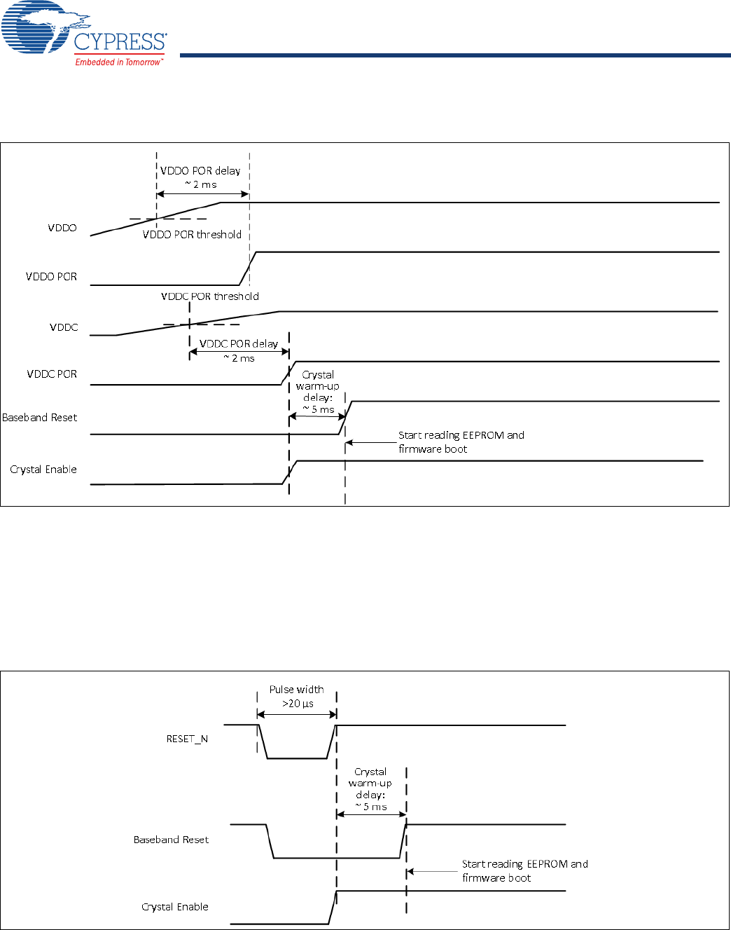
Internal Reset
Figure 11. Internal Reset Timing
External Reset (XRES)
The CYBLE-0130XX-00 has an integrated power-on reset circuit that completely resets all circuits to a known power-on state. An
external active low reset signal, XRES, can be used to put the CYBLE-0130XX-00 in the reset state. The XRES pin has an internal
pull-up resistor and, in most applications, it does not require that anything be connected to it. XRES should only be released after the
VDDO supply voltage level has been stabilized.
Figure 12. External Reset Timing

Document Number: 002-xxxxx Rev. ** Page 20 of 42
PRELIMINARY CYBLE-013025-00
CYBLE-013030-00
Integrated Radio Transceiver
The CYBLE-0130XX-00 has an integrated radio transceiver that is optimized for 2.4 GHz Bluetooth wireless systems. It has been
designed to provide low power, low cost, and robust communications for applications operating in the globally available 2.4 GHz unli-
censed ISM band. It is fully compliant with Bluetooth Radio Specification 4.1 and meets or exceeds the requirements to provide the
highest communication link quality of service.
Transmitter Path
The CYBLE-0130XX-00 features a fully integrated transmitter. The baseband transmit data is GFSK modulated in the 2.4 GHz ISM
band.
Digital Modulator
The digital modulator performs the data modulation and filtering required for the GFSK signal. The fully digital modulator minimizes
any frequency drift or anomalies in the modulation characteristics of the transmitted signal.
Power Amplifier
The CYBLE-0130XX-00 has an integrated power amplifier (PA) that can transmit up to +4 dBm for class 2 operation.
Receiver Path
The receiver path uses a low IF scheme to down convert the received signal for demodulation in the digital demodulator and bit syn-
chronizer. The receiver path provides a high degree of linearity, and an extended dynamic range to ensure reliable operation in the
noisy 2.4 GHz ISM band. The front-end topology, which has built-in out-of-band attenuation, enables the CYBLE-0130XX-00 to be
used in most applications without off-chip filtering.
Digital Demodulator and Bit Synchronizer
The digital demodulator and bit synchronizer take the low-IF received signal and perform an optimal frequency tracking and bit syn-
chronization algorithm.
Receiver Signal Strength Indicator
The radio portion of the CYBLE-0130XX-00 provides a receiver signal strength indicator (RSSI) to the baseband. This enables the
controller to take part in a Bluetooth power-controlled link by providing a metric of its own receiver signal strength to determine
whether the transmitter should increase or decrease its output power.
Local Oscillator
The local oscillator (LO) provides fast frequency hopping (1600 hops/second) across the 79 maximum available channels. The
CYBLE-0130XX-00 uses an internal loop filter.
Calibration
The CYBLE-0130XX-00 radio transceiver features a self-contained automated calibration scheme. No user interaction is required
during normal operation or during manufacturing to provide optimal performance. Calibration compensates for filter, matching net-
work, and amplifier gain and phase characteristics to yield radio performance within 2% of what is optimal. Calibration takes process
and temperature variations into account, and it takes place transparently during normal operation and hop setting times.
Internal LDO Regulator
The CYBLE-0130XX-00 has an integrated 1.2 V LDO regulator that provides power to the digital and RF circuits. The 1.2V LDO reg-
ulator operates from a 1.425 V to 3.63 V input supply with a 30 mA maximum load current.

Document Number: 002-xxxxx Rev. ** Page 21 of 42
PRELIMINARY CYBLE-013025-00
CYBLE-013030-00
Peripheral Transport Unit
Broadcom Serial Communications Interface
The CYBLE-0130XX-00 provides a 2-pin master BSC interface, which can be used to retrieve configuration information from an
external EEPROM or to communicate with peripherals such as track-ball or touch-pad modules, and motion tracking ICs used in
mouse devices. The BSC interface is compatible with I2C slave devices. The BSC does not support multimaster capability or flexible
wait-state insertion by either master or slave devices.
The following transfer clock rates are supported by the BSC:
n100 kHz
n400 kHz
n800 kHz (not a standard I2C-compatible speed.)
n1 MHz (Compatibility with high-speed I2C-compatible devices is not guaranteed.)
The following transfer types are supported by the BSC:
nRead (Up to 16 bytes can be read.)
nWrite (Up to 16 bytes can be written.)
nRead-then-Write (Up to 16 bytes can be read and up to 16 bytes can be written.)
nWrite-then-Read (Up to 16 bytes can be written and up to 16 bytes can be read.)
Hardware controls the transfers, requiring minimal firmware setup and supervision.
The clock pin (SCL) and data pin (SDA) are both open-drain I/O pins. Pull-up resistors external to the CYBLE-0130XX-00 are required
on both the SCL and SDA pins for proper operation.
USupport for changing the baud rate during normal HCI UART operation is included through a vendor-specific command that allows
the host to adjust the contents of the baud rate registers.
The CYBLE-0130XX-00 UART operates correctly with the host UART as long as the combined baud rate error of the two devices is
within ±5%.
Clock Frequencies
Peripheral Block
The peripheral blocks of the CYBLE-0130XX-00 all run from a single 128 kHz low-power RC oscillator. The oscillator can be turned
on at the request of any of the peripherals. If the peripheral is not enabled, it shall not assert its clock request line.
The keyboard scanner is a special case, in that it may drop its clock request line even when enabled, and then reassert the clock
request line if a keypress is detected.
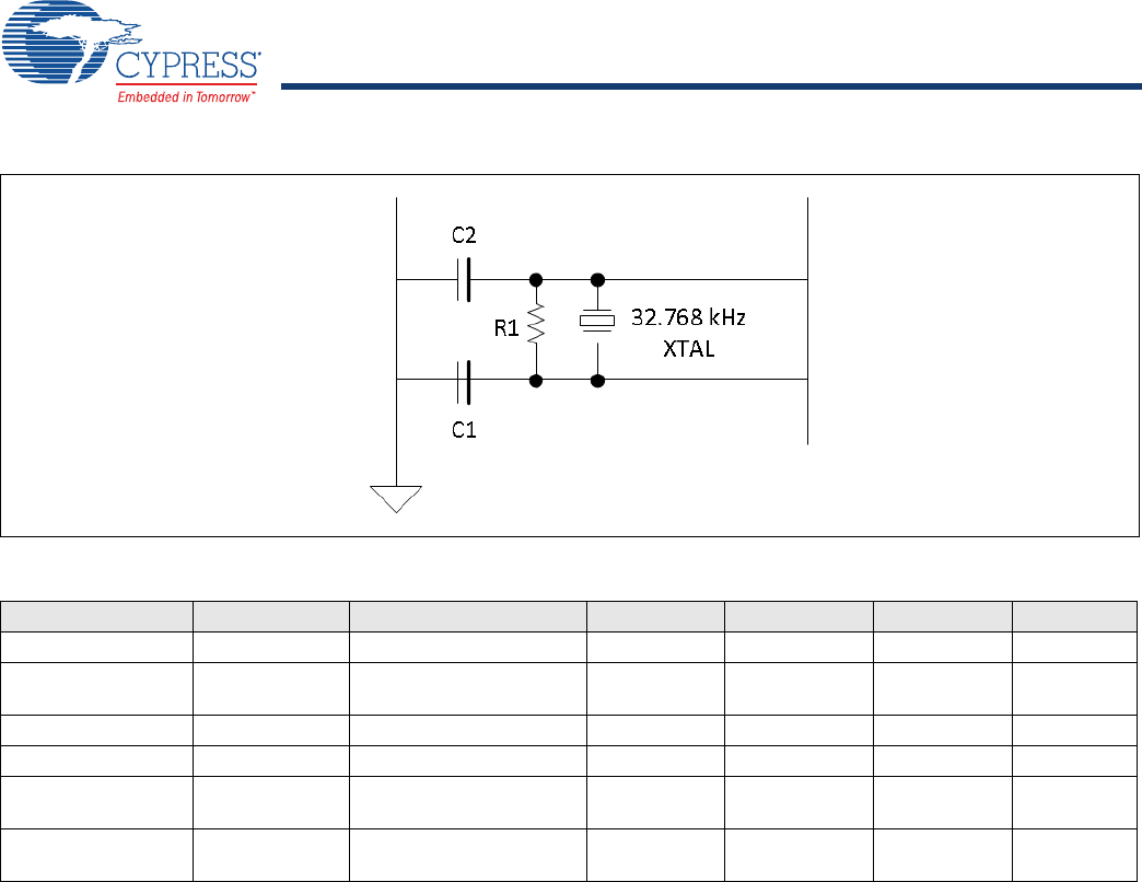
32 kHz Crystal Oscillator
Figure 13 shows the 32 kHz crystal (XTAL) oscillator with external components and Table 12 lists the oscillator’s
characteristics. It is a standard Pierce oscillator using a comparator with hysteresis on the output to create a
single-ended digital output. The hysteresis was added to eliminate any chatter when the input is around the threshold
of the comparator and is ~100 mV. This circuit can be operated with a 32 kHz or 32.768 kHz crystal oscillator or be driven
with a clock input at similar frequency. The default component values are: R1 = 10 M?, C1 = C2 = ~10 pF. The values
of C1 and C2 are used to fine-tune the oscillator.
Document Number: 002-xxxxx Rev. ** Page 22 of 42
PRELIMINARY CYBLE-013025-00
CYBLE-013030-00
Figure 13. 32 kHz Oscillator Block Diagram
GPIO Port
The CYBLE-0130XX-00 has 14 general-purpose I/Os (GPIOs) in the 32-pin package. All GPIOs support programmable pull-up and
pull-down resistors, and all support a 2 mA drive strength except P26, P27, and P28, which provide a 16 mA drive strength at 3.3V
supply. The following GPIOs are available:
n P0-P4
n P8/P33 only available for CYBLE-013030-00
n P11/P27 (Dual bonded, only one of two is available.)
n P12/P26 (Dual bonded, only one of two is available.)
n P13/P28 (Dual bonded, only one of two is available.)
n P14/P38 (Dual bonded, only one of two is available.)
n P15
n P24
n P25
n P32 - only available for CYBLE-013030-00
For a description of all GPIOs, see Ta ble 2 .
Table 12. XTAL Oscillator Characteristics
Parameter Symbol Conditions Minimum Typical Maximum Unit
Output frequency Foscout – – 32.768 – kHz
Frequency
tolerance
– Crystal dependent – 100 – ppm
Start-up time Tstartup – – – 500 ms
XTAL drive level Pdrv For crystal selection 0.5 – – ?W
XTAL series resis-
tance
Rseries For crystal selection – – 70 k?
XTAL shunt capaci-
tance
Cshunt For crystal selection – – 1.3 pF
Document Number: 002-xxxxx Rev. ** Page 23 of 42
PRELIMINARY CYBLE-013025-00
CYBLE-013030-00
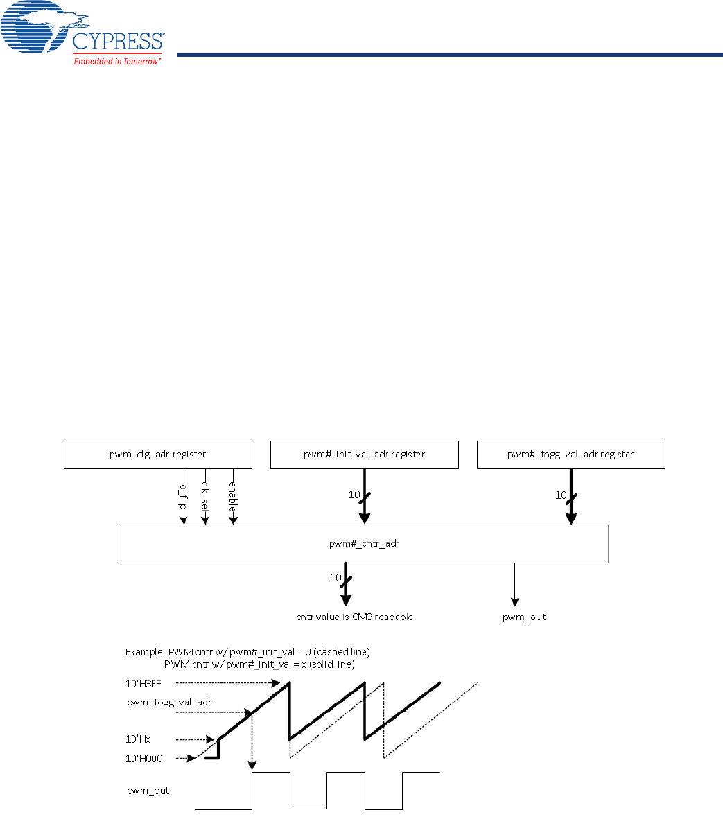
PWM
The CYBLE-0130XX-00 has four PWMs. The PWM module consists of the following:
nPWM0-3
nThe following GPIOs can be mapped as PWMs:
p. P26
p. P27
p. P14/P28 (Dual bonded, only one of two is available.)
p. P13 on P13/28
nPWM0–3. Each of the four PWM channels contains the following registers:
p10-bit initial value register (read/write)
p10-bit toggle register (read/write)
p10-bit PWM counter value register (read)
nPWM configuration register shared among PWM0–3 (read/write). This 12-bit register is used:
pTo configure each PWM channel
pTo select the clock of each PWM channel
pTo change the phase of each PWM channel
Figure 14 shows the structure of one PWM.
Figure 14. PWM Block Diagram

Document Number: 002-xxxxx Rev. ** Page 24 of 42
PRELIMINARY CYBLE-013025-00
CYBLE-013030-00
Power Management Unit
The Power Management Unit (PMU) provides power management features that can be invoked by software through power
management registers or packet-handling in the baseband core.
RF Power Management
The BBC generates power-down control signals for the transmit path, receive path, PLL, and power amplifier to the 2.4 GHz trans-
ceiver, which then processes the power-down functions accordingly.
Host Controller Power Management
Power is automatically managed by the firmware based on input device activity. As a power-saving task, the firmware controls the
disabling of the on-chip regulator when in deep sleep mode.
BBC Power Management
There are several low-power operations for the BBC:
nPhysical layer packet handling turns RF on and off dynamically within packet TX and RX.
nBluetooth-specified low-power connection mode. While in these low-power connection modes, the CYBLE-0130XX-00 runs on the
Low Power Oscillator and wakes up after a predefined time period.
The CYBLE-0130XX-00 automatically adjusts its power dissipation based on user activity. The following power modes are supported:
nActive mode
nIdle mode
nSleep mode
nHIDOFF (Deep Sleep) mode
nTimed Deep Sleep mode
The CYBLE-0130XX-00 transitions to the next lower state after a programmable period of user inactivity. Busy mode is immediately
entered when user activity resumes.
nIn HIDOFF (Deep Sleep) mode, the CYBLE-0130XX-00 baseband and core are powered off by disabling power to LDOOUT. The
VDDO domain remains powered up and will turn the remainder of the chip on when it detects user events. This mode minimizes
chip power consumption and is intended for long periods of inactivity.
Document Number: 002-xxxxx Rev. ** Page 25 of 42
PRELIMINARY CYBLE-013025-00
CYBLE-013030-00
Electrical Characteristics
Tab l e 13 shows the maximum electrical rating for voltages referenced to VDD pin.
Tab l e 14 shows the power supply characteristics for the range TJ = 0 to 125×C.
Table 15 shows the specifications for the ADC characteristics.
Table 13. Maximum Electrical Rating
Rating Symbol Value Unit
VDD –3.8 V
Voltage on input or output pin – VSS – 0.3 to VDD + 0.3 V
Operating ambient temperature range Topr –30 to +85 °C
Storage temperature range Tstg –40 to +125 °C
Table 14. Power Supply
Parameter Description Minimum1
1. Overall performance degrades beyond minimum and maximum supply voltages.
Typical MaximumaUnit
VDD Power Supply Input 2.3 – 3.6 V
VDD_RIPPLE Maximum power supply ripple for VDD input voltage – – 100 mV
Table 15. ADC Specifications
Parameter Symbol Conditions Min Typ Max Unit
Number of Input channels – – – 9 – –
Channel switching rate fch – – – 133.33 kch/s
Input signal range Vinp –0–3.63V
Reference settling time – Changing refsel 7.5 – – μs
Input resistance Rinp Effective, single ended – 500 – kΩ
Input capacitance Cinp –––5pF
Conversion rate fC– 5.859 – 187 kHz
Conversion time TC– 5.35 – 170.7 μs
Resolution R – – 16 – bits
Effective number of bits – In specified performance range – See
Tab l e 8 on
page 17
–
Absolute voltage
measurement error
– Using on-chip ADC firmware driver – ±2 – %
Current I Iavdd1p2 + Iavdd3p3 –– 1 mA
Power P – – 1.5 – mW
Leakage current Ileakage T = 25×C – – 100 nA
Power-up time Tpowerup –––200µs
Integral nonlinearity3INL In guaranteed performance range – – 1 LSB1
Differential nonlin-
earity<Superscript>1 DNL In guaranteed performance range – – 1 LSB1

Document Number: 002-xxxxx Rev. ** Page 26 of 42
PRELIMINARY CYBLE-013025-00
CYBLE-013030-00
Table 16 shows the specifications for the digital voltage levels.
1. LSBs are expressed at the 10-bit level.
Table 16. Digital Levels1
1. This table is also applicable to VDDMEM domain.
Characteristics Symbol Min Typ Max Unit
Input low voltage VIL ––0.4V
Input high voltage VIH 0.75 × VDDO – – V
Input low voltage (VDDO = 1.62V) VIL ––0.4V
Input high voltage (VDDO = 1.62V) VIH 1.2 ––V
Output low voltage2
2. At the specified drive current for the pad.
VOL ––0.4V
Output high voltage2VOH VDDO – 0.4 – – V
Input capacitance (VDDMEM domain) CIN –0.12–pF
Document Number: 002-xxxxx Rev. ** Page 27 of 42
PRELIMINARY CYBLE-013025-00
CYBLE-013030-00
Table 17 shows the specifications for current consumption.
Table 17. Current Consumption1
1. Currents measured between power terminals (Vdd) using 90% efficient DC-DC converter at 3V.
Operational Mode Conditions Typ Max Unit
Receive Receiver and baseband are both operating, 100% ON. 9.8 10.0mA
Transmit Transmitter and baseband are both operating, 100% ON. 9.19.3 mA
Sleep Internal LPO is in use. 12.0 13.0 µA
–0.65–
Table 18. Power Supply Current Consumption
Power Supply Advertisement Rates Typ Max Unit
VDD 20 ms 1.96 mA
Document Number: 002-xxxxx Rev. ** Page 28 of 42
PRELIMINARY CYBLE-013025-00
CYBLE-013030-00
RF Specifications
Table 19. Receiver RF Specifications
Parameter Mode and Conditions Min Typ Max Unit
Receiver Section1
1. 30.8% PER.
Frequency range – 2402 – 2480 MHz
RX sensitivity (standard) 0.1%BER, 1 Mbps – –94 – dBm
RX sensitivity (low current) – –91.5 – dBm
Input IP3 – –16 – – dBm
Maximum input – –10 – – dBm
Interference Performance<Superscript>1,2
2. Desired signal is 3 dB above the reference sensitivity level (defined as –70 dBm).
C/I cochannel 0.1%BER – – 21 dB
C/I 1 MHz adjacent channel 0.1%BER – – 15 dB
C/I 2 MHz adjacent channel 0.1%BER – – –17 dB
C/I ℜ≥ 3 MHz adjacent channel 0.1%BER – – –27 dB
C/I image channel 0.1%BER – – –9.0 dB
C/I 1 MHz adjacent to image channel 0.1%BER – – –15 dB
Out-of-Band Blocking Performance (CW)1,2
30 MHz to 2000 MHz 0.1%BER3
3. Measurement resolution is 10 MHz.
– –30.0 – dBm
2003 MHz to 2399 MHz 0.1%BER4
4. Measurement resolution is 3 MHz.
– –35 – dBm
2484 MHz to 2997 MHz 0.1%BER4– –35 – dBm
3000 MHz to 12.75 GHz 0.1%BER5
5. Measurement resolution is 25 MHz.
– –30.0 – dBm
Spurious Emissions
30 MHz to 1 GHz – – – –57.0 dBm
1 GHz to 12.75 GHz – – – –55.0 dBm
Table 20. Transmitter RF Specifications
Parameter Minimum Typical Maximum Unit
Transmitter Section
Frequency range 2402 – 2480 MHz
Output power adjustment range –20 – 4 dBm
Default output power – 4.0 – dBm
Output power variation – 2.0 – dB
Adjacent Channel Power
|M – N| = 2 – – –20 dBm
|M – N| ℜ≥ 3 – – –30 dBm
Out-of-Band Spurious Emission
Document Number: 002-xxxxx Rev. ** Page 29 of 42
PRELIMINARY CYBLE-013025-00
CYBLE-013030-00
30 MHz to 1 GHz – – –36.0 dBm
1 GHz to 12.75 GHz – – –30.0 dBm
1.8 GHz to 1.9 GHz – – –47.0 dBm
5.15 GHz to 5.3 GHz – – –47.0 dBm
LO Performance
Initial carrier frequency tolerance – – ±150 kHz
Frequency Drift
Frequency drift – – ±50 kHz
Drift rate – – 20 kHz/50 µs
Frequency Deviation
Average deviation in payload
(sequence used is 00001111)
225 – 275 kHz
Maximum deviation in payload
(sequence used is 10101010)
185– – kHz
Channel spacing – 2 – MHz
Table 20. Transmitter RF Specifications (continued)
Parameter Minimum Typical Maximum Unit
Document Number: 002-xxxxx Rev. ** Page 30 of 42
PRELIMINARY CYBLE-013025-00
CYBLE-013030-00
Timing and AC Characteristics
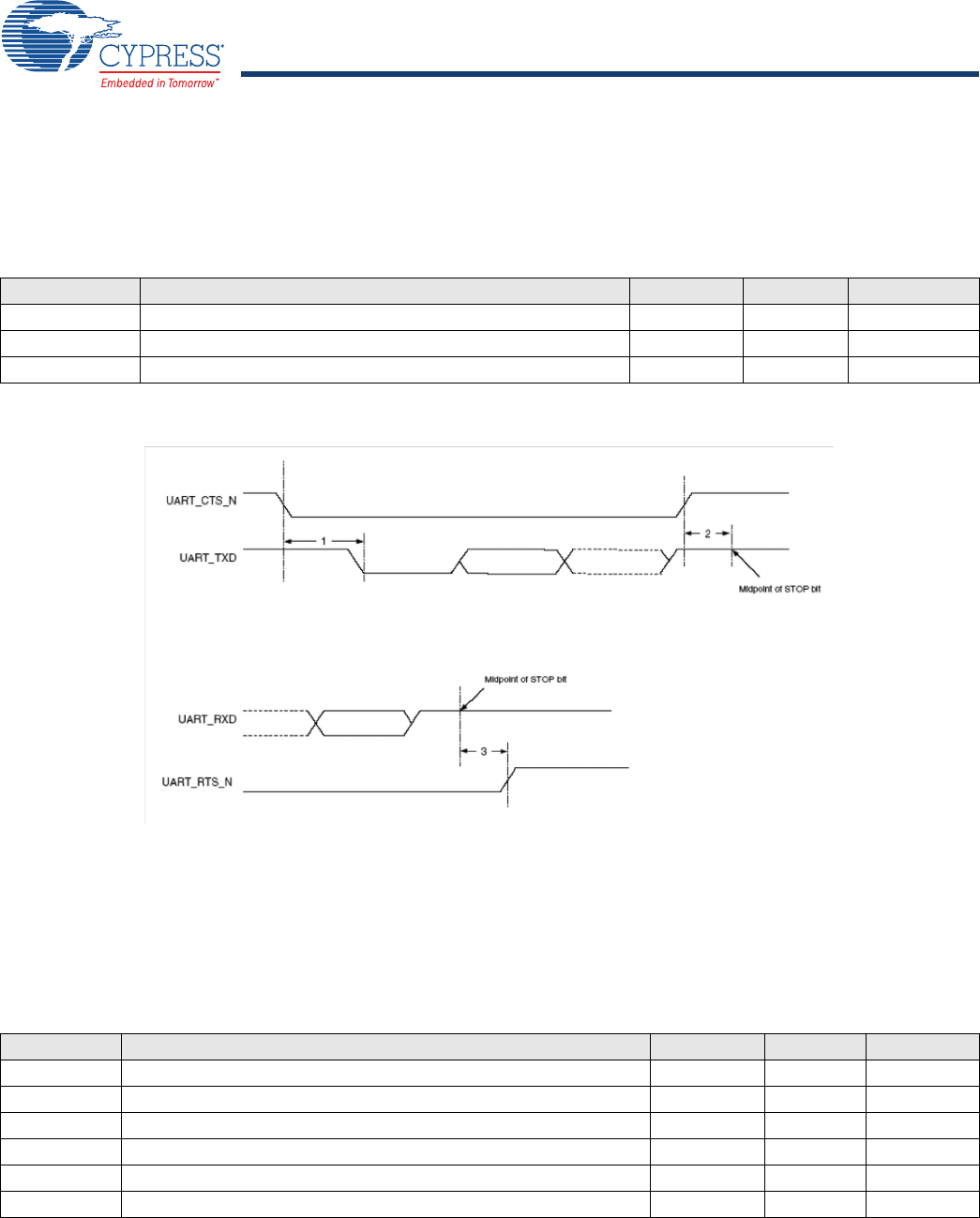
In this section, use the numbers listed in the Reference column of each table to interpret the following timing diagrams.
UART Timing
Figure 15. UART Timing
SPI Timing
The SPI interface supports clock speeds up to 12 MHz with VDDIO ≥ 2.2V. The supported clock speed is 6 MHz when 2.2V > VDDIO
≥ 1.62V.
Figure 16 and Figure 17 show the timing requirements when operating in SPI Mode 0 and 2, and SPI Mode 1 and 3, respectively.
Table 21. UART Timing Specifications
Reference Characteristics Min Max Unit
1 Delay time, UART_CTS_N low to UART_TXD valid – 24 Baud out cycles
2 Setup time, UART_CTS_N high before midpoint of stop bit – 10 ns
3 Delay time, midpoint of stop bit to UART_RTS_N high – 2 Baud out cycles
Table 22. SPI Interface Timing Specifications
Reference Characteristics Min Typ Max
1 Time from CSN asserted to first clock edge 1 SCK 100 ?
2 Master setup time – ¾ SCK –
3 Master hold time ¾ SCK – –
4 Slave setup time – ¾ SCK –
5Slave hold time ¾ SCK––
6 Time from last clock edge to CSN deasserted 1 SCK 10 SCK 100
Document Number: 002-xxxxx Rev. ** Page 31 of 42
PRELIMINARY CYBLE-013025-00
CYBLE-013030-00
Figure 16. SPI Timing – Mode 0 and 2
Figure 17. SPI Timing – Mode 1 and 3
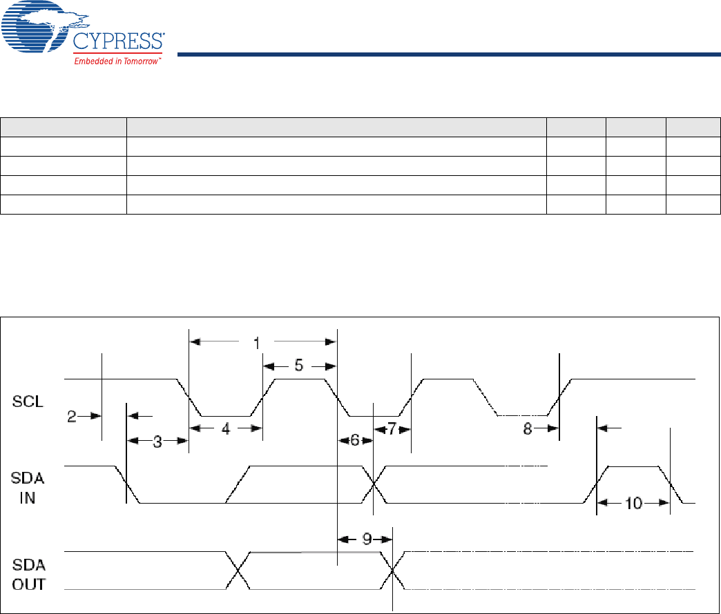
BSC Interface Timing
Table 23. BSC Interface Timing Specifications
Reference Characteristics Min Max Unit
1 Clock frequency – 100 kHz
400
800
1000
2 START condition setup time 650 – ns
3 START condition hold time 280 – ns
4 Clock low time 650 – ns
5 Clock high time 280 – ns
6 Data input hold time10 – ns
Document Number: 002-xxxxx Rev. ** Page 32 of 42
PRELIMINARY CYBLE-013025-00
CYBLE-013030-00
Figure 18. BSC Interface Timing Diagram
7 Data input setup time 100 – ns
8 STOP condition setup time 280 – ns
9 Output valid from clock – 400 ns
10 Bus free time2650 – ns
1. As a transmitter, 300 ns of delay is provided to bridge the undefined region of the falling edge of SCL to avoid unintended generation of START
or STOP conditions.
2. Time that the cbus must be free before a new transaction can start.
Table 23. BSC Interface Timing Specifications
Reference Characteristics Min Max Unit
Document Number: 002-xxxxx Rev. ** Page 33 of 42
PRELIMINARY CYBLE-013025-00
CYBLE-013030-00
Environmental Specifications
Environmental Compliance
This Cypress BLE module is produced in compliance with the Restriction of Hazardous Substances (RoHS) and Halogen-Free (HF)
directives. The Cypress module and components used to produce this module are RoHS and HF compliant.
RF Certification
The CYBLE-0130XX-00 module will be certified under the following RF certification standards at production release.
nFCC: WAP3025
nCE
nIC: 7922A-3025
nMIC: TBD
Safety Certification
The CYBLE-0130XX-00 module complies with the following safety regulations:
nUnderwriters Laboratories, Inc. (UL): Filing E331901
nCSA
nTUV
Environmental Conditions
Tab l e 24 describes the operating and storage conditions for the Cypress BLE module.
ESD and EMI Protection
Exposed components require special attention to ESD and electromagnetic interference (EMI).
A grounded conductive layer inside the device enclosure is suggested for EMI and ESD performance. Any openings in the enclosure
near the module should be surrounded by a grounded conductive layer to provide ESD protection and a low-impedance path to ground.
Device Handling: Proper ESD protocol must be followed in manufacturing to ensure component reliability.
Table 24. Environmental Conditions for CYBLE-0130XX-00
Description Minimum Specification Maximum Specification
Operating temperature −30 °C 85 °C
Operating humidity (relative, non-condensation) 5% 85%
Thermal ramp rate – 3 °C/minute
Storage temperature –40 °C 85 °C
Storage temperature and humidity – 85 °C at 85%
ESD: Module integrated into system Components[6] –15 kV Air
2.0 kV Contact
Note
6. This does not apply to the RF pins (ANT).

Document Number: 002-xxxxx Rev. ** Page 34 of 42
PRELIMINARY CYBLE-013025-00
CYBLE-013030-00
Regulatory Information
FCC
FCC NOTICE:
The device CYBLE-0130XX-00 complies with Part 15 of the FCC Rules. The device meets the requirements for modular transmitter
approval as detailed in FCC public Notice DA00-1407.transmitter Operation is subject to the following two conditions: (1) This device
may not cause harmful interference, and (2) This device must accept any interference received, including interference that may cause
undesired operation.
CAUTION:
The FCC requires the user to be notified that any changes or modifications made to this device that are not expressly approved by
Cypress Semiconductor may void the user's authority to operate the equipment.
This equipment has been tested and found to comply with the limits for a Class B digital device, pursuant to Part 15 of the FCC Rules.
These limits are designed to provide reasonable protection against harmful interference in a residential installation. This equipment
generates uses and can radiate radio frequency energy and, if not installed and used in accordance with the instructions,ê may cause
harmful interference to radio communications. However, there is no guarantee that interference will not occur in a particular installation.
If this equipment does cause harmful interference to radio or television reception, which can be determined by turning the equipment
off and on, the user is encouraged to try to correct the interference by one or more of the following measures:
nReorient or relocate the receiving antenna.
nIncrease the separation between the equipment and receiver.
nConnect the equipment into an outlet on a circuit different from that to which the receiver is connected.
nConsult the dealer or an experienced radio/TV technician for help
LABELING REQUIREMENTS:
The Original Equipment Manufacturer (OEM) must ensure that FCC labelling requirements are met. This includes a clearly visible
label on the outside of the OEM enclosure specifying the appropriate Cypress Semiconductor FCC identifier for this product as well
as the FCC Notice above. The FCC identifier is FCC ID: WAP3025.
In any case the end product must be labeled exterior with "Contains FCC ID: WAP3025"
ANTENNA WARNING:
This device is tested with a standard SMA connector and with the antennas listed below. When integrated in the OEMs product, these
fixed antennas require installation preventing end-users from replacing them with non-approved antennas. Any antenna not in the
following table must be tested to comply with FCC Section 15.203 for unique antenna connectors and Section 15.247 for emissions.
RF EXPOSURE:
To comply with FCC RF Exposure requirements, the Original Equipment Manufacturer (OEM) must ensure to install the approved
antenna in the previous.
The preceding statement must be included as a CAUTION statement in manuals, for products operating with the approved antennas
in Table 7 on page 12, to alert users on FCC RF Exposure compliance. Any notification to the end user of installation or removal
instructions about the integrated radio module is not allowed.
The radiated output power of CYBLE-0130XX-00 with the trace antenna is far below the FCC radio frequency exposure limits.
Nevertheless, use CYBLE-0130XX-00 in such a manner that minimizes the potential for human contact during normal operation.
End users may not be provided with the module installation instructions. OEM integrators and end users must be provided with
transmitter operating conditions for satisfying RF exposure compliance.

Document Number: 002-xxxxx Rev. ** Page 35 of 42
PRELIMINARY CYBLE-013025-00
CYBLE-013030-00
Industry Canada (IC) Certification
CYBLE-0130XX-00 is licensed to meet the regulatory requirements of Industry Canada (IC),
License: IC: 7922A-3025
Manufacturers of mobile, fixed or portable devices incorporating this module are advised to clarify any regulatory questions and ensure
compliance for SAR and/or RF exposure limits. Users can obtain Canadian information on RF exposure and compliance from
www.ic.gc.ca.
This device has been designed to operate with the antennas listed in Ta ble 7 on page 12, having a maximum gain of 0.5 dBi. Antennas
not included in this list or having a gain greater than 0.5 dBi are strictly prohibited for use with this device. The required antenna
impedance is 50 ohms. The antenna used for this transmitter must not be co-located or operating in conjunction with any other antenna
or transmitter.
IC NOTICE:
The device CYBLE-0130XX-00 including the built-in trace antenna complies with Canada RSS-GEN Rules. The device meets the
requirements for modular transmitter approval as detailed in RSS-GEN. Operation is subject to the following two conditions: (1) This
device may not cause harmful interference, and (2) This device must accept any interference received, including interference that
may cause undesired operation.
IC RADIATION EXPOSURE STATEMENT FOR CANADA
This device complies with Industry Canada licence-exempt RSS standard(s). Operation is subject to the following two conditions: (1)
this device may not cause interference, and (2) this device must accept any interference, including interference that may cause
undesired operation of the device.
Le présent appareil est conforme aux CNR d'Industrie Canada applicables aux appareils radio exempts de licence. L'exploitation est
autorisée aux deux conditions suivantes : (1) l'appareil ne doit pas produire de brouillage, et (2) l'utilisateur de l'appareil doit accepter
tout brouillage radioélectrique subi, même si le brouillage est susceptible d'en compromettre le fonctionnement.
LABELING REQUIREMENTS:
The Original Equipment Manufacturer (OEM) must ensure that IC labelling requirements are met. This includes a clearly visible label
on the outside of the OEM enclosure specifying the appropriate Cypress Semiconductor IC identifier for this product as well as the IC
Notice above. The IC identifier is 7922A-3025. In any case, the end product must be labeled in its exterior with "Contains IC:
7922A-3025"
European R&TTE Declaration of Conformity
Hereby, Cypress Semiconductor declares that the Bluetooth module CYBLE-013025-00 complies with the essential requirements and
other relevant provisions of Directive 1999/5/EC. As a result of the conformity assessment procedure described in Annex III of the
Directive 1999/5/EC, the end-customer equipment should be labeled as follows:
All versions of the CYBLE-0130XX-00 in the specified reference design can be used in the following countries: Austria, Belgium,
Cyprus, Czech Republic, Denmark, Estonia, Finland, France, Germany, Greece, Hungary, Ireland, Italy, Latvia, Lithuania, Luxem-
bourg, Malta, Poland, Portugal, Slovakia, Slovenia, Spain, Sweden, The Netherlands, the United Kingdom, Switzerland, and Norway.

Document Number: 002-xxxxx Rev. ** Page 36 of 42
PRELIMINARY CYBLE-013025-00
CYBLE-013030-00
MIC Japan
CYBLE-0130XX-00 is certified as a module with type certification number TBD. End products that integrate CYBLE-013025-00 do not
need additional MIC Japan certification for the end product.
End product can display the certification label of the embedded module.
Document Number: 002-xxxxx Rev. ** Page 37 of 42
PRELIMINARY CYBLE-013025-00
CYBLE-013030-00
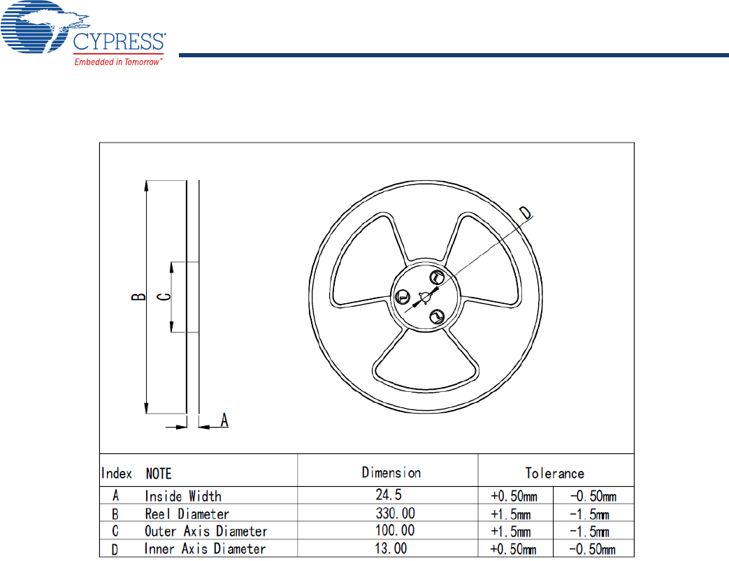
Packaging
The CYBLE-0130XX-00 is offered in tape and reel packaging. Figure 19 details the tape dimensions used for the CYBLE-0130XX-00.
Figure 19. CYBLE-0130XX-00 Tape Dimensions (TBD)
Figure 20 details the orientation of the CYBLE-0130XX-00 in the tape as well as the direction for unreeling.
Figure 20. Component Orientation in Tape and Unreeling Direction (TBD)
Table 25. Solder Reflow Peak Temperature
Module Part Number Package Maximum Peak Temperature Maximum Time at Peak Temperature No. of Cycles
CYBLE-0130XX-00 14-pad SMT 260 °C 30 seconds 2
Table 26. Package Moisture Sensitivity Level (MSL), IPC/JEDEC J-STD-2
Module Part Number Package MSL
CYBLE-0130XX-00 31-pad SMT MSL 3
Document Number: 002-xxxxx Rev. ** Page 38 of 42
PRELIMINARY CYBLE-013025-00
CYBLE-013030-00
Figure 21 details reel dimensions used for the CYBLE-0130XX-00.
Figure 21. Reel Dimensions
The CYBLE-0130XX-00 is designed to be used with pick-and-place equipment in an SMT manufacturing environment. The
center-of-mass for the CYBLE-0130XX-00 is detailed in Figure 22.
Figure 22. CYBLE-0130XX-00 Center of Mass (TBD)
Document Number: 002-xxxxx Rev. ** Page 39 of 42
PRELIMINARY CYBLE-013025-00
CYBLE-013030-00
Ordering Information
Tab l e 27 lists the CYBLE-0130XX-00 part number and features. Tab le 28 lists the reel shipment quantities for the CYBLE-0130XX-00.
The CYBLE-0130XX-00 is offered in tape and reel packaging. The CYBLE-0130XX-00 ships in a reel size of TBD.
For additional information and a complete list of Cypress Semiconductor BLE products, contact your local Cypress sales
representative. To locate the nearest Cypress office, visit our website.
Table 27. Ordering Information
Part Number
CPU
Speed
(MHz)
Flash
Size (KB)
RAM
Size (KB) UART BSC
(I2C) PWM Package Packaging
CYBLE-013025-00 24 128 60 Yes Yes 4 31-SMT Tape and Reel
CYBLE-013030-00 24 – 60 Yes Yes 4 31-SMT Tape and Reel
Table 28. Tape and Reel Package Quantity and Minimum Order Amount
Description Minimum Reel Quantity Maximum Reel Quantity Comments
Reel Quantity TBD TBD Ships in TBD unit reel quantities.
Minimum Order Quantity (MOQ) TBD – –
Order Increment (OI) TBD – –
U.S. Cypress Headquarters Address 198 Champion Court, San Jose, CA 95134
U.S. Cypress Headquarter Contact Info (408) 943-2600
Cypress website address http://www.cypress.com
Document Number: 002-xxxxx Rev. ** Page 40 of 42
PRELIMINARY CYBLE-013025-00
CYBLE-013030-00
Acronyms Document Conventions
Units of Measure
Table 29. Acronyms Used in this Document
Acronym Description
BLE Bluetooth Low Energy
Bluetooth SIG Bluetooth Special Interest Group
CE European Conformity
CSA Canadian Standards Association
EMI electromagnetic interference
ESD electrostatic discharge
FCC Federal Communications Commission
GPIO general-purpose input/output
IC Industry Canada
IDE integrated design environment
KC Korea Certification
MIC Ministry of Internal Affairs and Communications
(Japan)
PCB printed circuit board
RX receive
QDID qualification design ID
SMT
surface-mount technology; a method for
producing electronic circuitry in which the
components are placed directly onto the surface
of PCBs
TCPWM timer, counter, pulse width modulator (PWM)
TUV Germany: Technischer Überwachungs-Verein
(Technical Inspection Association)
TX transmit
Table 30. Units of Measure
Symbol Unit of Measure
°C degree Celsius
kV kilovolt
mA milliamperes
mm millimeters
mV millivolt
μA microamperes
μm micrometers
MHz megahertz
GHz gigahertz
Vvolt
Document Number: 002-xxxxx Rev. ** Page 41 of 42
PRELIMINARY CYBLE-013025-00
CYBLE-013030-00
Document History Page
Document Title: CYBLE-0130XX-00 EZ-BLE™ WICED Module
Document Number: 002-XXXXX
Revision ECN Orig. of
Change
Submission
Date Description of Change
** PRELIM-
INARY
DSO Preliminary datasheet for CYBLE-0130XX-00 module.

Document Number: 002-xxxxx Rev. ** Revised April 10, 2017 Page 42 of 42
PRELIMINARY
CYBLE-013025-00
CYBLE-013030-00
© Cypress Semiconductor Corporation, 2017. This document is the property of Cypress Semiconductor Corporation and its subsidiaries, including Spansion LLC ("Cypress"). This document, including
any software or firmware included or referenced in this document ("Software"), is owned by Cypress under the intellectual property laws and treaties of the United States and other countries worldwide.
Cypress reserves all rights under such laws and treaties and does not, except as specifically stated in this paragraph, grant any license under its patents, copyrights, trademarks, or other intellectual
property rights. If the Software is not accompanied by a license agreement and you do not otherwise have a written agreement with Cypress governing the use of the Software, then Cypress hereby
grants you a personal, non-exclusive, nontransferable license (without the right to sublicense) (1) under its copyright rights in the Software (a) for Software provided in source code form, to modify and
reproduce the Software solely for use with Cypress hardware products, only internally within your organization, and (b) to distribute the Software in binary code form externally to end users (either
directly or indirectly through resellers and distributors), solely for use on Cypress hardware product units, and (2) under those claims of Cypress's patents that are infringed by the Software (as provided
by Cypress, unmodified) to make, use, distribute, and import the Software solely for use with Cypress hardware products. Any other use, reproduction, modification, translation, or compilation of the
Software is prohibited.
TO THE EXTENT PERMITTED BY APPLICABLE LAW, CYPRESS MAKES NO WARRANTY OF ANY KIND, EXPRESS OR IMPLIED, WITH REGARD TO THIS DOCUMENT OR ANY SOFTWARE
OR ACCOMPANYING HARDWARE, INCLUDING, BUT NOT LIMITED TO, THE IMPLIED WARRANTIES OF MERCHANTABILITY AND FITNESS FOR A PARTICULAR PURPOSE. To the extent
permitted by applicable law, Cypress reserves the right to make changes to this document without further notice. Cypress does not assume any liability arising out of the application or use of any
product or circuit described in this document. Any information provided in this document, including any sample design information or programming code, is provided only for reference purposes. It is
the responsibility of the user of this document to properly design, program, and test the functionality and safety of any application made of this information and any resulting product. Cypress products
are not designed, intended, or authorized for use as critical components in systems designed or intended for the operation of weapons, weapons systems, nuclear installations, life-support devices or
systems, other medical devices or systems (including resuscitation equipment and surgical implants), pollution control or hazardous substances management, or other uses where the failure of the
device or system could cause personal injury, death, or property damage ("Unintended Uses"). A critical component is any component of a device or system whose failure to perform can be reasonably
expected to cause the failure of the device or system, or to affect its safety or effectiveness. Cypress is not liable, in whole or in part, and you shall and hereby do release Cypress from any claim,
damage, or other liability arising from or related to all Unintended Uses of Cypress products. You shall indemnify and hold Cypress harmless from and against all claims, costs, damages, and other
liabilities, including claims for personal injury or death, arising from or related to any Unintended Uses of Cypress products.
Cypress, the Cypress logo, Spansion, the Spansion logo, and combinations thereof, WICED, PSoC, CapSense, EZ-USB, F-RAM, and Traveo are trademarks or registered trademarks of Cypress in
the United States and other countries. For a more complete list of Cypress trademarks, visit cypress.com. Other names and brands may be claimed as property of their respective owners.
Sales, Solutions, and Legal Information
Worldwide Sales and Design Support
Cypress maintains a worldwide network of offices, solution centers, manufacturer’s representatives, and distributors. To find the office
closest to you, visit us at Cypress Locations.
Products
ARM® Cortex® Microcontrollers cypress.com/arm
Automotive cypress.com/automotive
Clocks & Buffers cypress.com/clocks
Interface cypress.com/interface
Internet of Things cypress.com/iot
Memory cypress.com/memory
Microcontrollers cypress.com/mcu
PSoC cypress.com/psoc
Power Management ICs cypress.com/pmic
Touch Sensing cypress.com/touch
USB Controllers cypress.com/usb
Wireless Connectivity cypress.com/wireless
PSoC® Solutions
PSoC 1 | PSoC 3 | PSoC 4 | PSoC 5LP
Cypress Developer Community
Forums | WICED IOT Forums | Projects | Video | Blogs |
Training | Components
Technical Support
cypress.com/support