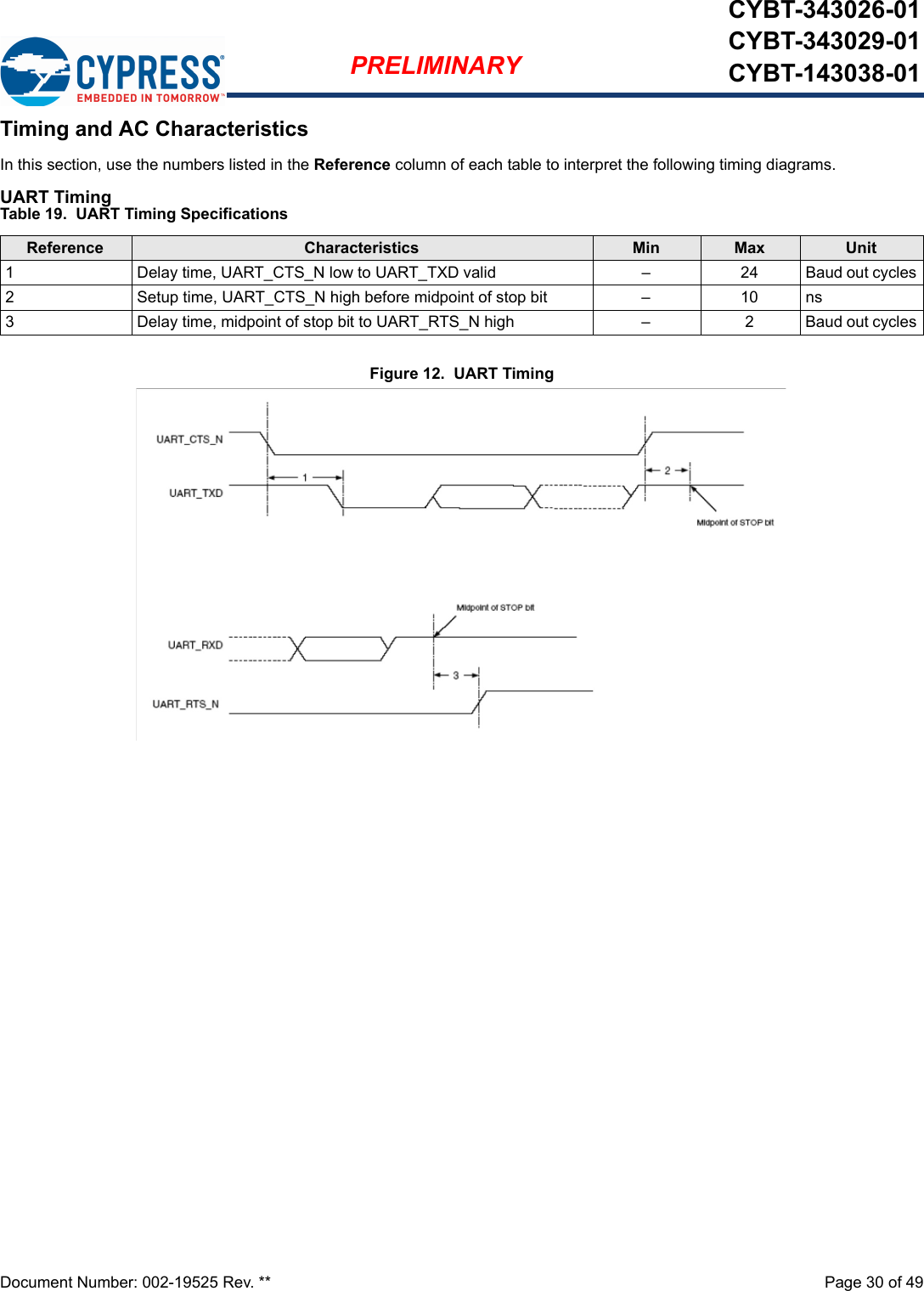
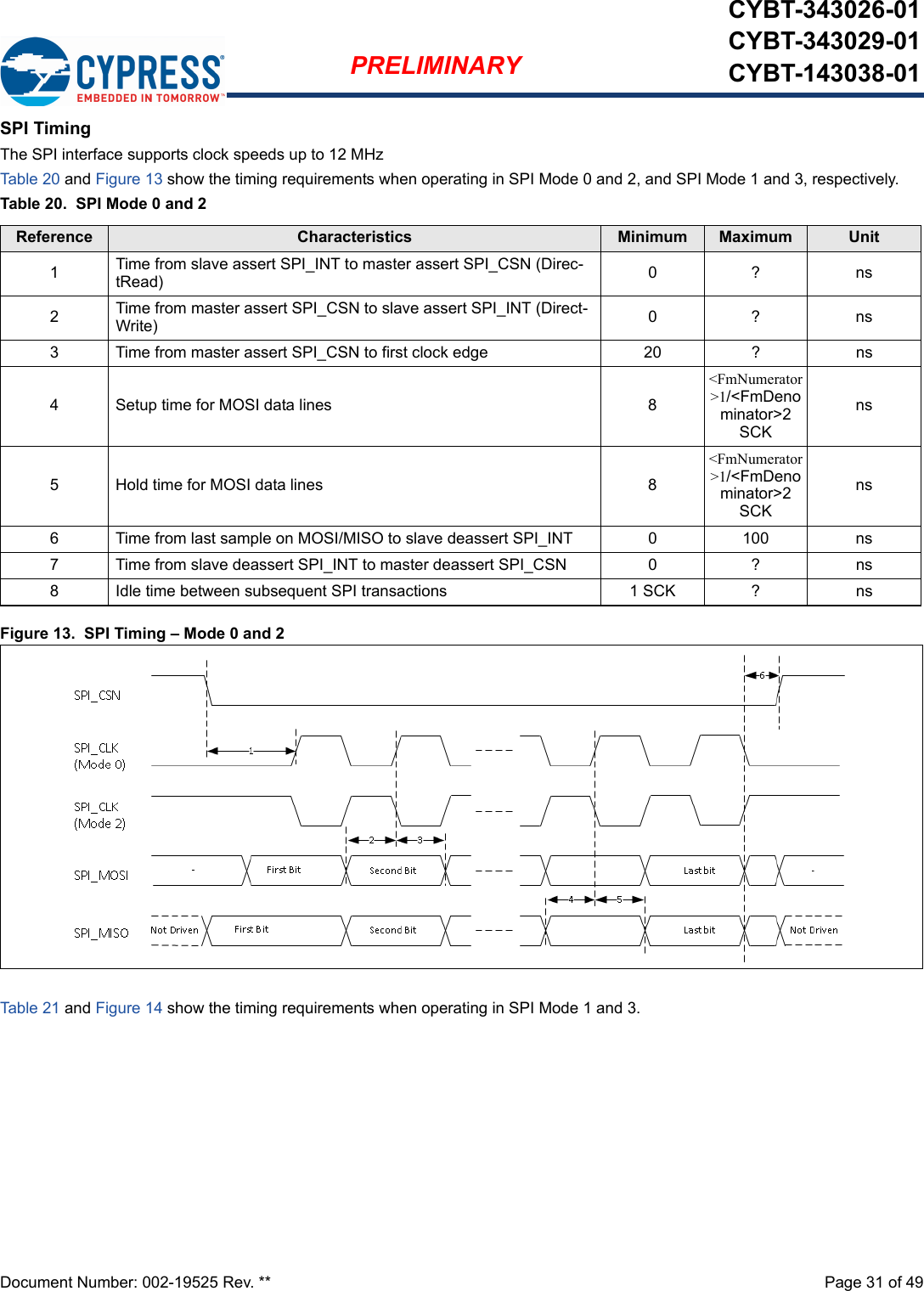
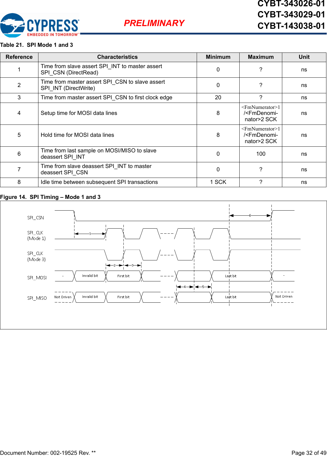
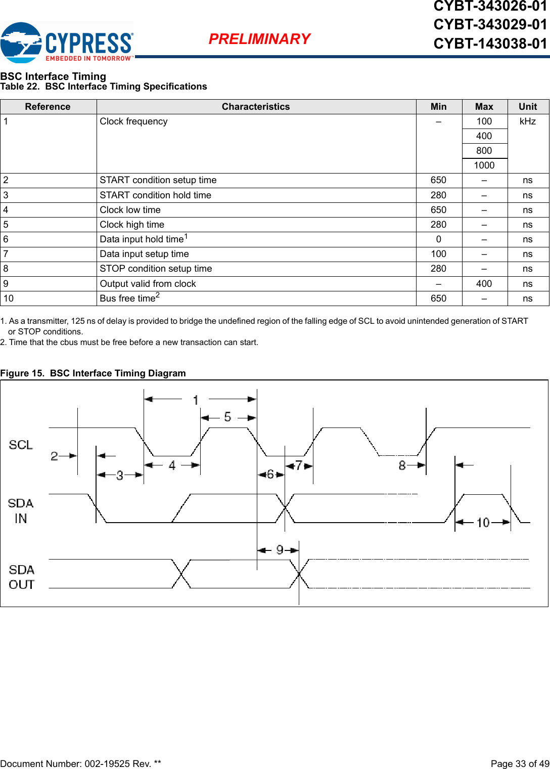
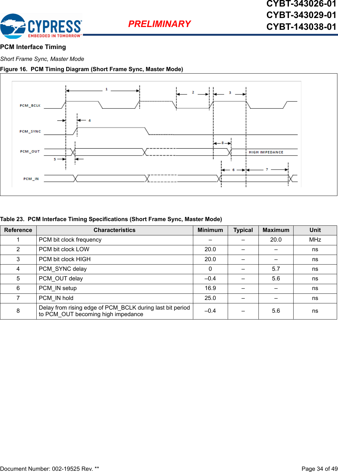
Cypress Semiconductor 3026 Bluetooth wireless EZ-BT Module User Manual CYBT 013033 01 EZ BT Module
Cypress Semiconductor Bluetooth wireless EZ-BT Module CYBT 013033 01 EZ BT Module
UserManual.wiki
>
Cypress Semiconductor
>
3026 User Manual
>
User Manual
Contents
1.
User Manual
2.
User Guide
User Manual
Navigation menu
Upload a User Manual
Namespaces
Wiki Guide
HTML
PDF
Info
Views
User Manual
Discussion / Help
Navigation
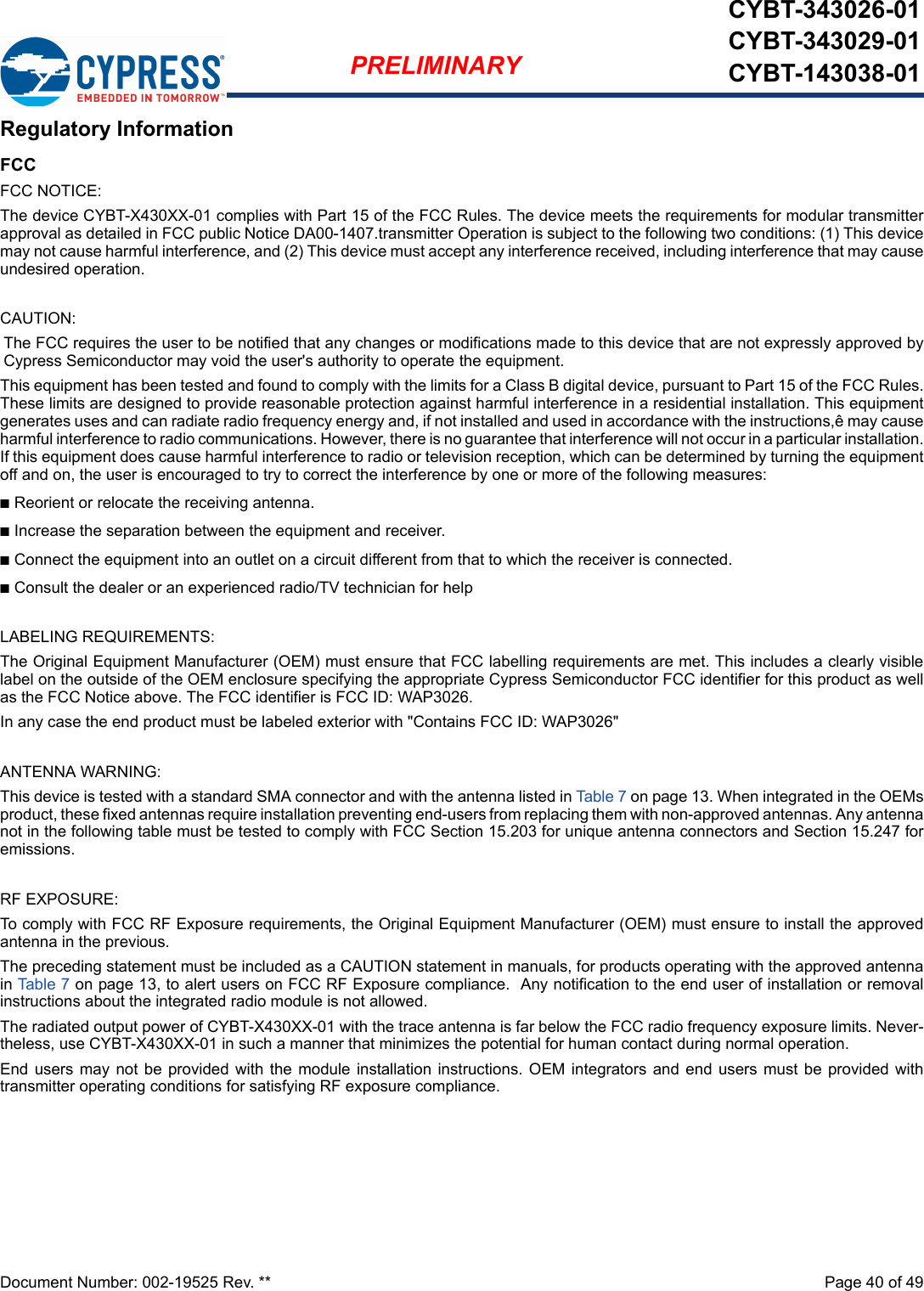
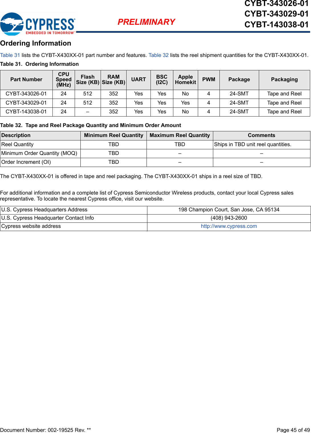
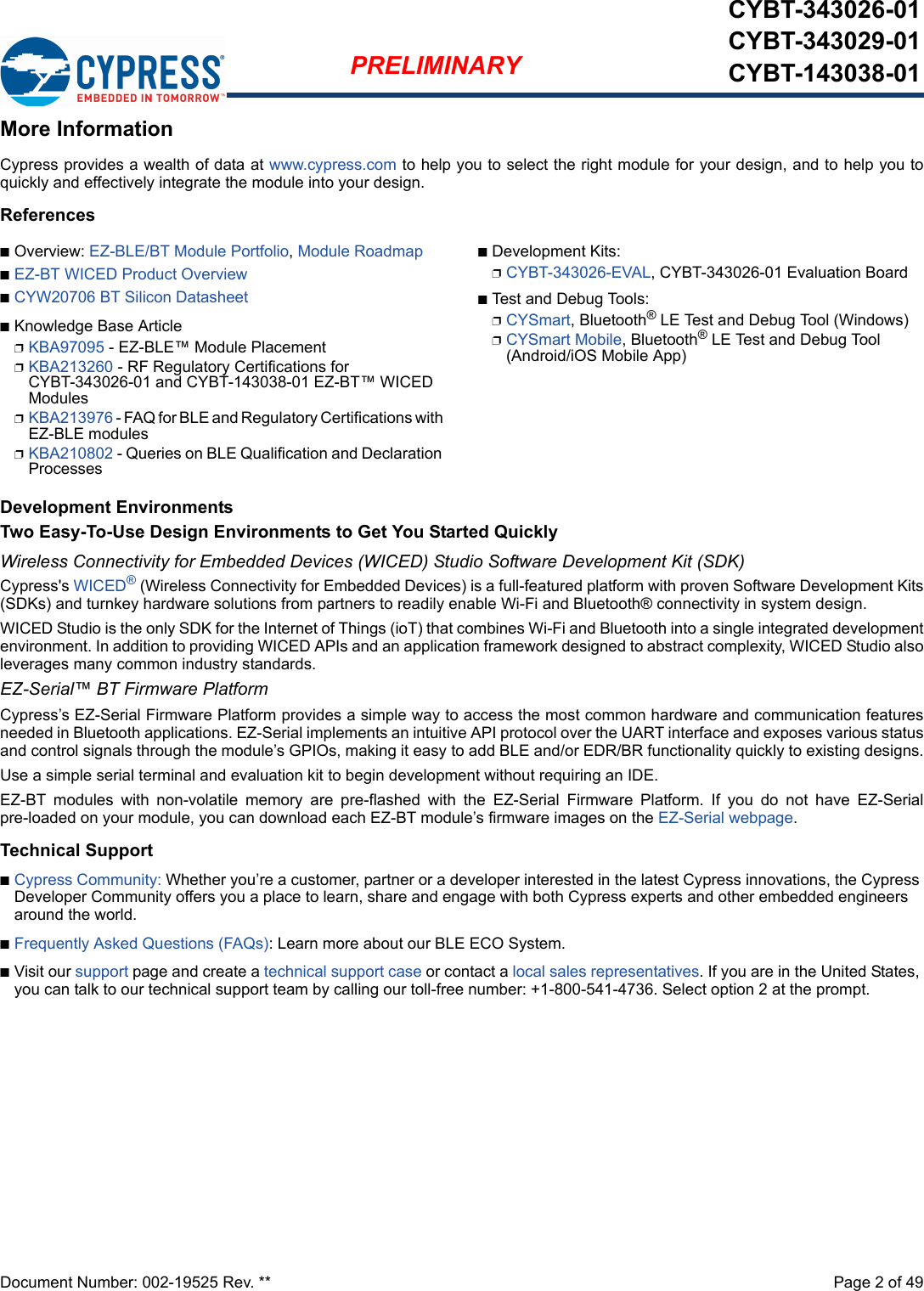
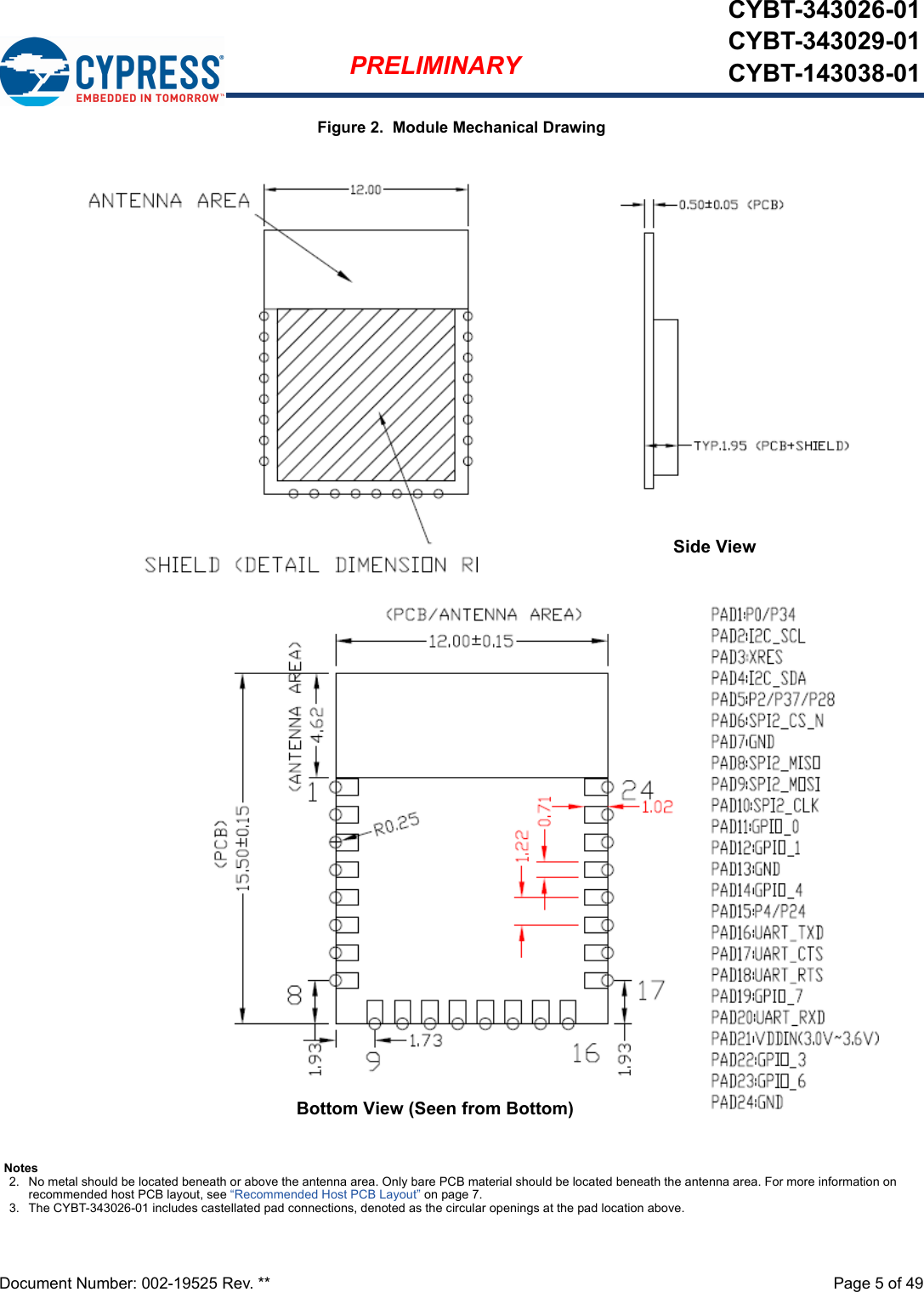
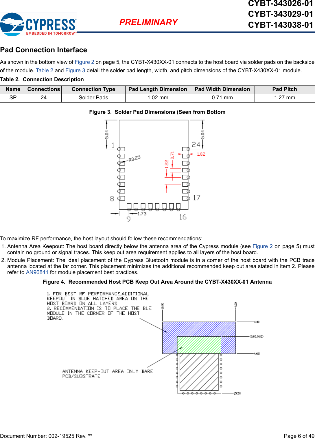
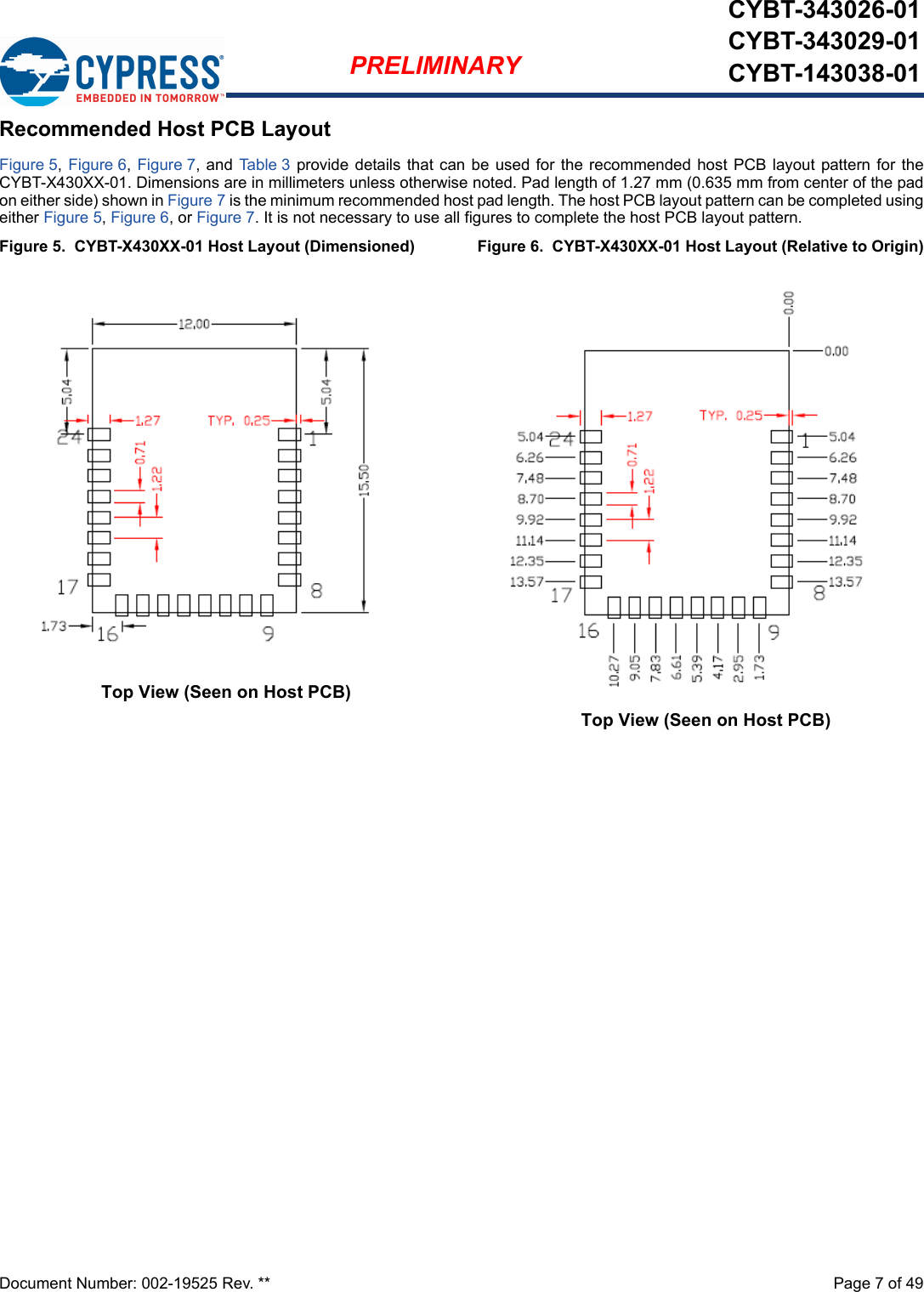
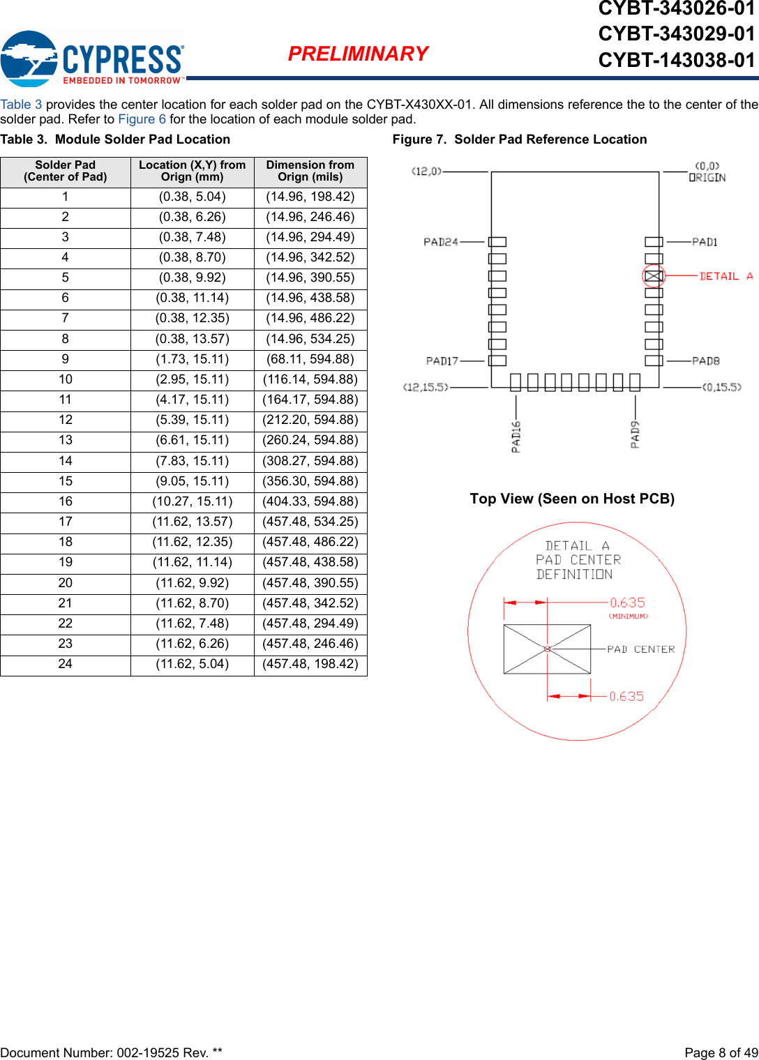
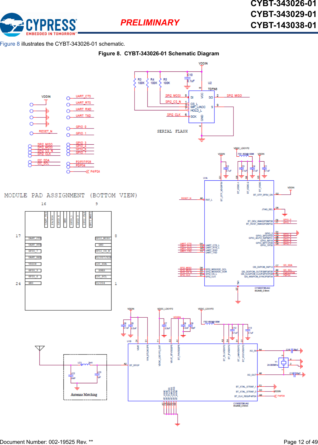
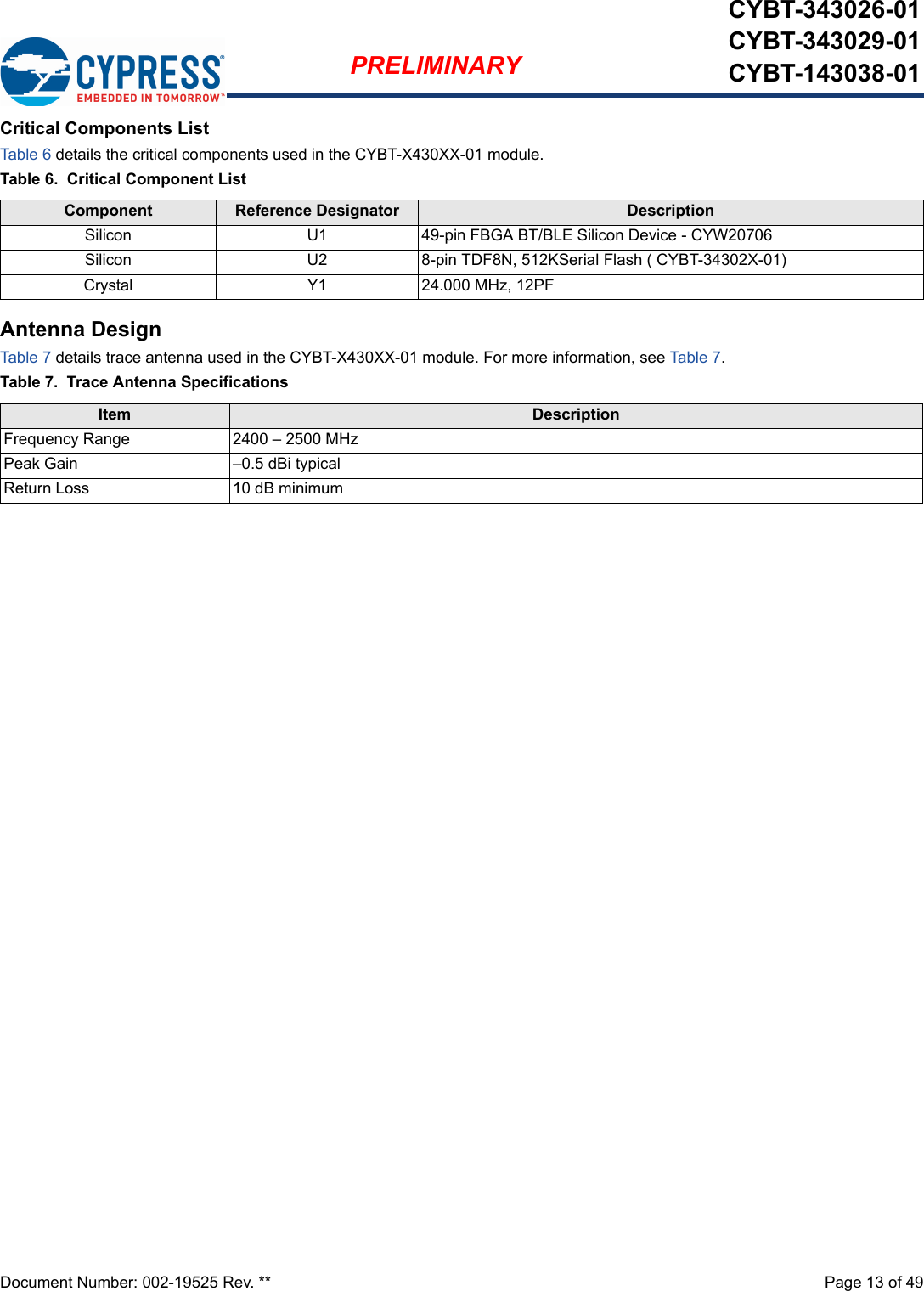
![PRELIMINARYCYBT-343026-01CYBT-343029-01CYBT-143038-01EZ-BT™ WICED ModuleCypress Semiconductor Corporation • 198 Champion Court • San Jose,CA 95134-1709 • 408-943-2600Document Number: 002-19525 Rev. ** Revised May 31, 2017General DescriptionThe CYBT-X430XX-01 is a fully integrated Bluetooth SmartReady wireless module. The CYBT-X430XX-01 includes anonboard crystal oscillator, passive components, flash memory,and the Cypress CYW20706 silicon device. Refer to theCYW20706 datasheet for additional details on the capabilities ofthe silicon device used in this module. The CYBT-X430XX-01 supports peripheral functions (ADC andPWM), UART and USB communication, and a Bluetooth audiointerface. The CYBT-X430XX-01 includes a royalty-free BLEstack compatible with Bluetooth 4.2 in a 12.0 × 15.5 × 1.95 mmpackage.The CYBT-343026-01 includes 512KB of onboard serial flashmemory and is designed for stand-alone opperation. TheCYBT-343029-01 has the same characterisitcs as theCYBT-343026-01, but also include an on-board AppleAuthentication co-processor for use with Apple products such asHomekit. The CYBT-143038-01 does not contain onboard flash,requiring hosted control or application RAM upload operatingmodes. The CYBT-143038-01 can also interface to externalflash on the host board. The CYBT-X430XX-01 utilizes anintegrated power amplifer to achieve Class I or Class II outputpower capability. The CYBT-X430XX-01 is fully qualified by Bluetooth SIG and istargeted at applications requiring cost optimized BLE wirelessconnectivity. Module DescriptionnModule size: 12.00 mm × 15.50 mm × 1.95 mm nBluetooth LE 4.2 Smart Ready modulepQDID: WAP3026pDeclaration ID: 7922A-3026nCertified to FCC, IC, MIC, and CE regulationsnCastelated solder pad connections for ease-of-usen512-KB on-module serial flash memory ( CYBT-34302X-01)nUp to 10 GPIOsnTemperature range: –30 °C to +85 °CnCortex-M3 32-bit processor nMaximum TX output power: p+12 dbm for Bluetooth EDRp+9 dBm for Bluetooth Low EnergynRX Receive Sensitivity: p–93.5 dBm for Bluetooth Classic p–96.5 dBm for Bluetooth Low EnergyPower Consumption[1]nTX average current consumption: 12.5 mA (EDR) Class-IInRX average current consumption: 20.0 mA (EDR)nLow power mode supportpSleep: 120 uA Functional Capabilitiesn10-bit auxiliary ADC with nine analog channelsnSerial Communications interface compatible with I2C slavesnSerial Peripheral Interface (SPI) support for both master and slave modesnHCI interface through USB or UARTnPCM/I2S Auido interfacen2-wire Global Coexistence Interface (GCI)nBluetooth wideband speech supportnIntegrated peripherals such as PWM, ADC, Triac controlnProgrammable output power controlnMaximum of 100 LE ConnectionsnSupports extended synchronous connections (eSCO), for enhanced voice quality by allowing for retransmission of dropped packetsBenefitsCYBT-X430XX-01 provides all necessary components requiredto operate BLE and/or EDR/BR communication standards. nProven hardware design ready to usenDual-mode operatoin eliminates the need for multiple modulesnCost optimized for applications without space constraintsnNon-volatile memory for self-sufficient operation and Over-the-air updates ( CYBT-34302X-01 only)nBluetooth SIG Listed with QDID and Declaration ID nFully certified module eliminates the time needed for design, development and certification processesnWICED™ STUDIO 4.0 provides an easy-to-use integrated design environment (IDE) to configure, develop, and program a Bluetooth applicationnPre-programmed EZ-Serial firmware platform to allow for easy-to-use out of the box Bluetooth connectivityNotes1. The values in this section were calculated for a 90% efficient DC-DC at 3V in HCI mode, and based on a Class I configurationbench-marked at Class II. Lower values are expected for a class II configuration using an external LPO and corresponding PAconfiguration](https://usermanual.wiki/Cypress-Semiconductor/3026.User-Manual/User-Guide-3461008-Page-1.png)
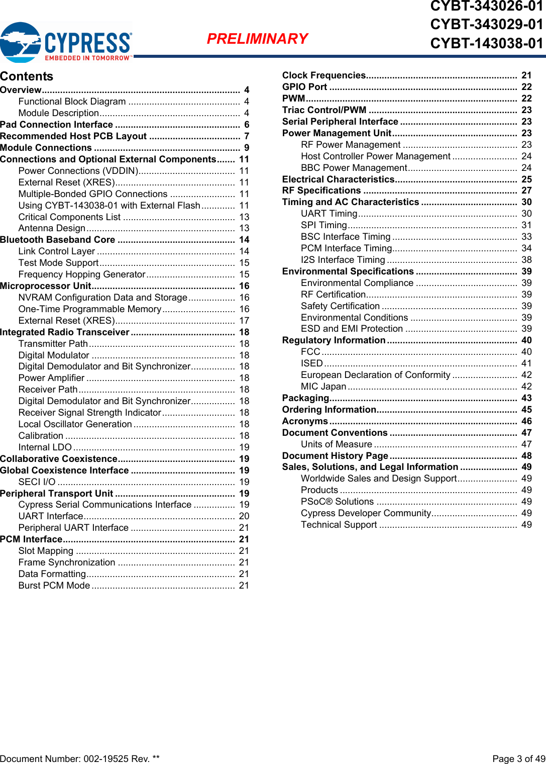
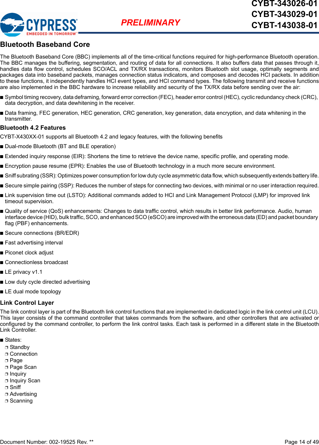
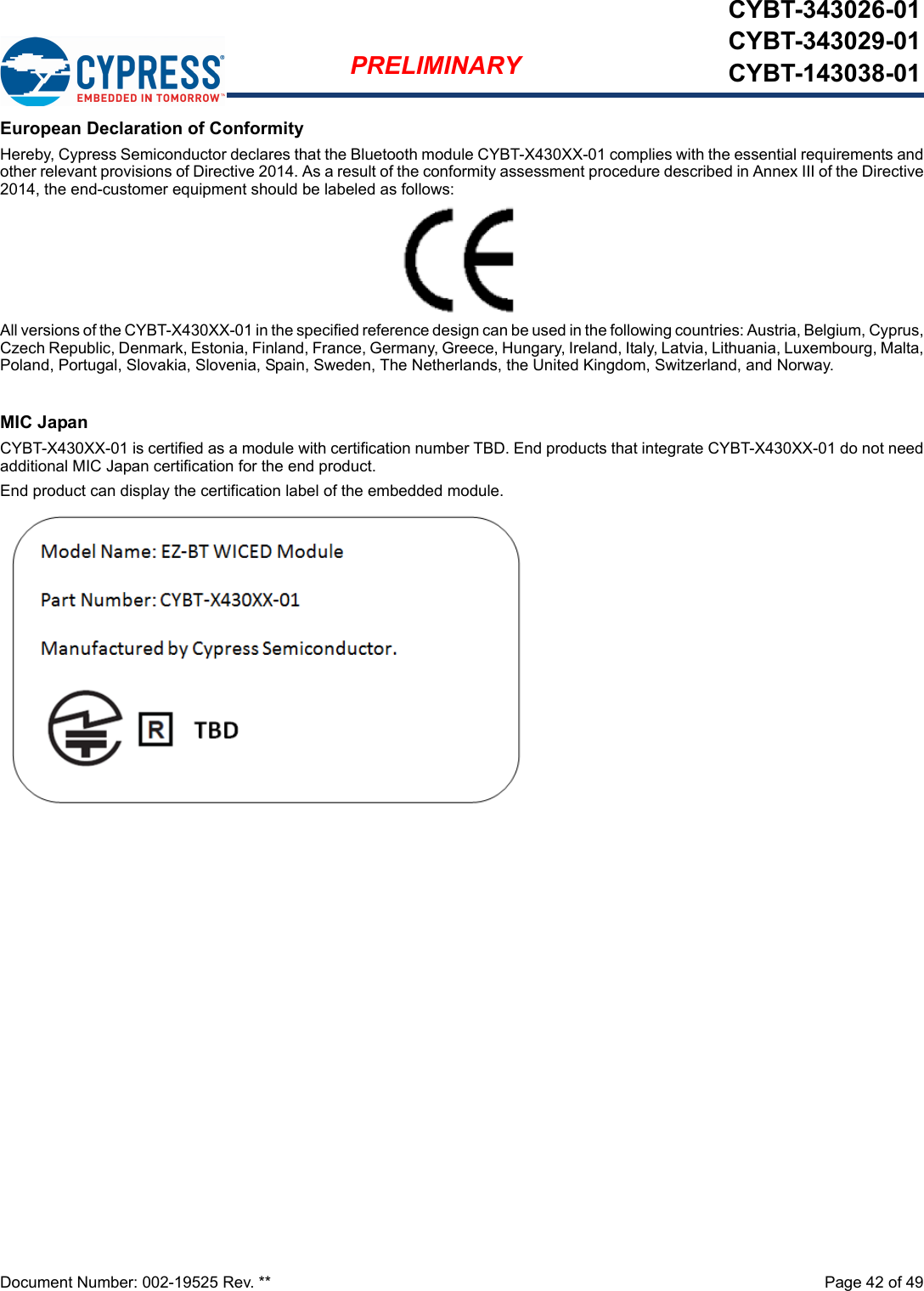
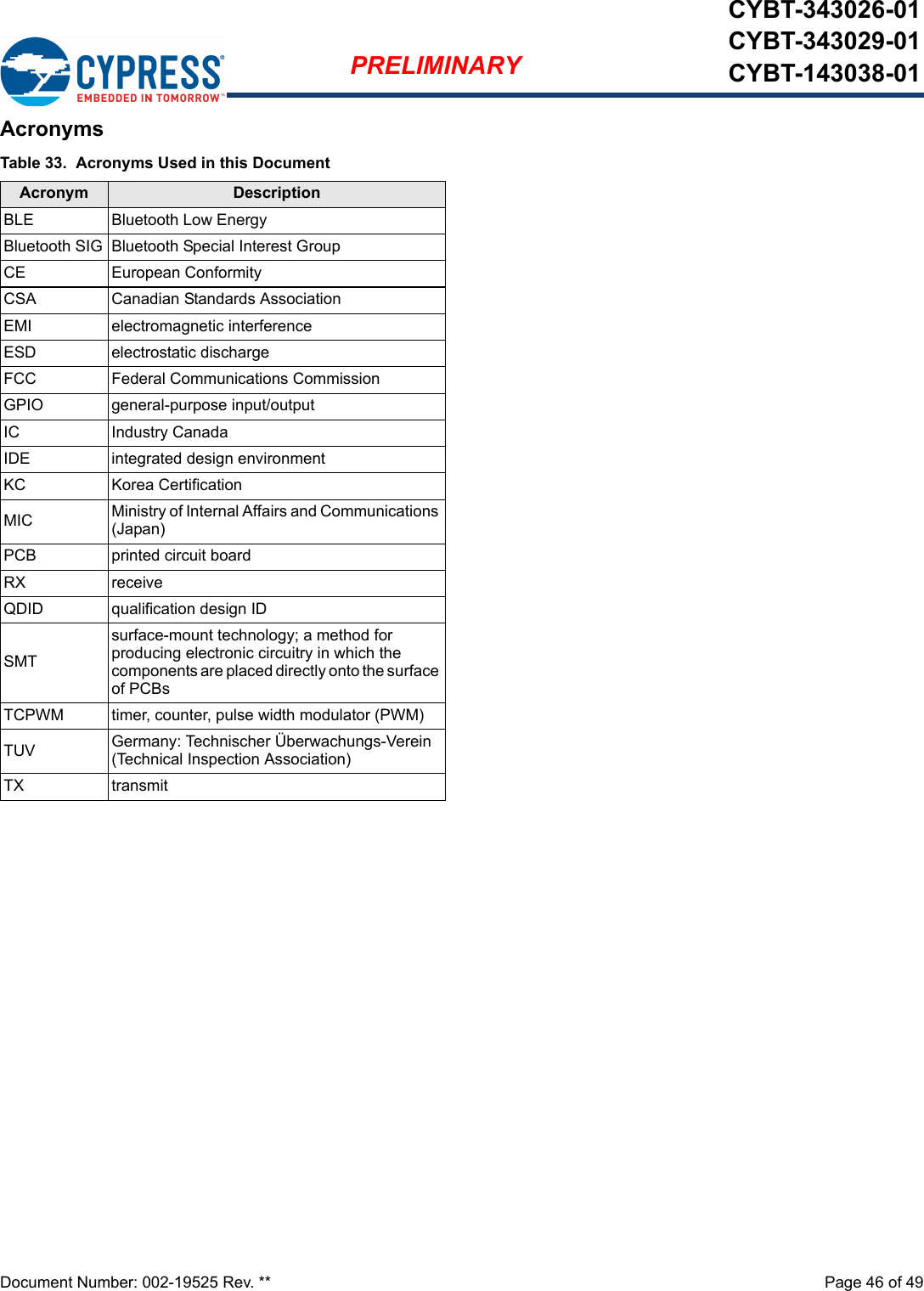
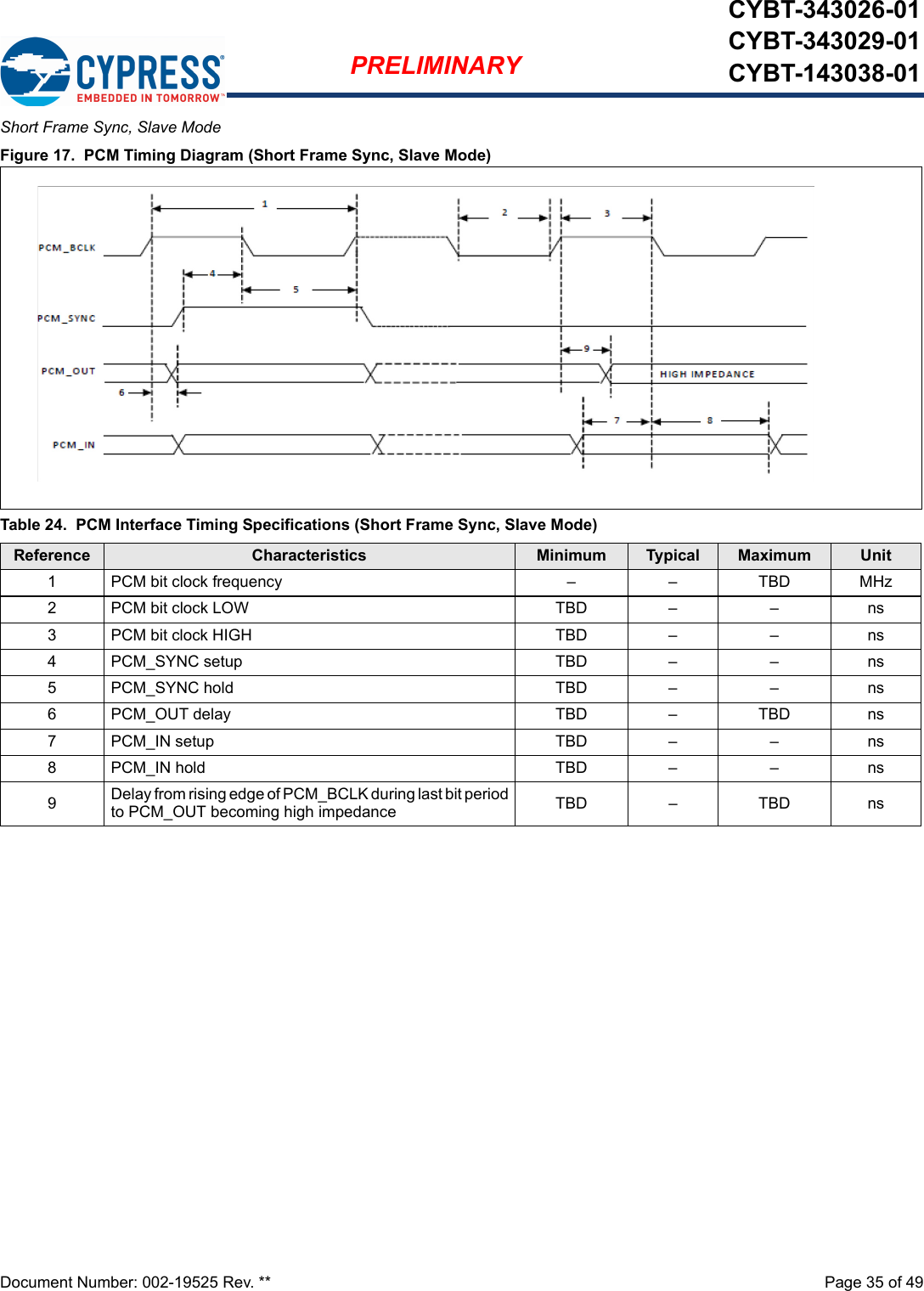
![Document Number: 002-19525 Rev. ** Page 22 of 49PRELIMINARYCYBT-343026-01CYBT-343029-01CYBT-143038-01GPIO PortThe CYBT-X430XX-01 has 24 general-purpose I/Os (GPIOs). All GPIOs support programmable pull-ups and are capable of drivingup to 8 mA at 3.3V or 4 mA at 1.8V, except chip P26, P27, P28, and P29, which are capable of driving up to 16 mA at 3.3V or 8 mAat 1.8V.The Following GPIOs on the module pads are available:nPAD 11 GPIO_0: GPIO_0/P36/P38 (triple bonded; only one of three is available)nPAD 12 GPIO_1: GPIO_1/P25/P32 (triple bonded; only one of three is available)nPAD 22 GPIO_3: GPIO_3/P27/P33 (triple bonded; only one of three is available)nPAD 14 GPIO_4: GPIO_4/LPO_IN/P6/P31 (quadruple bonded; only of four is available)nPAD 23 GPIO_6: GPIO_6/P11/P26 (triple bonded; only one of three is available)nPAD 19 GPIO_7: GPIO_7/P30 (Dual bonded; only one of two is available)nPAD 15 P4/P24: BT_CLK_REQ/P4/P24 (triple bonded; only one of three is available)nPAD 4 I2C_SDA: I2S_PCM_IN/P12 (dual bonded; only one of two is available)nPAD 2 I2C_SCL: I2S_PCM_OUT/P3/P29/P35 (quadruple bonded; only one of four is available)nPAD 5 P2/P37/P28: I2S_PCM_CLK/P2/P28/P37 (quadruple bonded; only one of four is available)nPAD 1 P0/34: I2S_WS_PCM_SYNC/P0/P34 (triple bonded; only onAll of these pins can be programmed as ADC inputs.Port 26–Port 29 in PAD 23/PAD 22/PAD 5/PAD 2P[26:29] in PAD 23/PAD 22/PAD 5/PAD 2 consists of four pins. All pins are capable of sinking up to 16 mA for LEDs. These pins alsohave PWM functionality, which can be used for LED dimming.For a description of the capabilities of all GPIOs, see Tab le 4 and Table 5 .PWMThe CYBT-X430XX-01 has four PWMs. The PWM module consists of the following: nPWM0-3nThe following GPIOs can be mapped as PWMs, module pad shown in [ ]:pP26 on P12/P26 [Pad 5]pP27 on P11/P27 [Pad 4]pP14 on P14/P38 [Pad 7]pP13 on P13/P28 [Pad 8]nPWM1-4: Each of the four PWM channels contains the following registers: p10-bit initial value register (read/write)p10-bit toggle register (read/write)p10-bit PWM counter value register (read)nPWM configuration register shared among PWM1-4 (read/write). This 12-bit register is used: pTo configure each PWM channelpTo select the clock of each PWM channelpTo change the phase of each PWM channel Figure 11 shows the structure of one PWM.](https://usermanual.wiki/Cypress-Semiconductor/3026.User-Manual/User-Guide-3461008-Page-22.png)
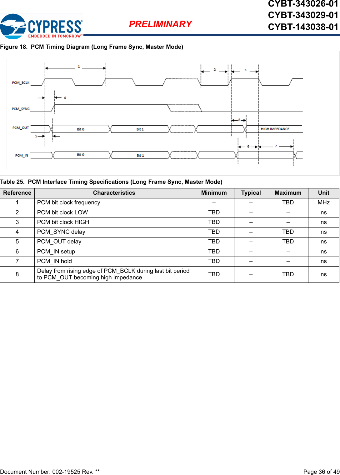
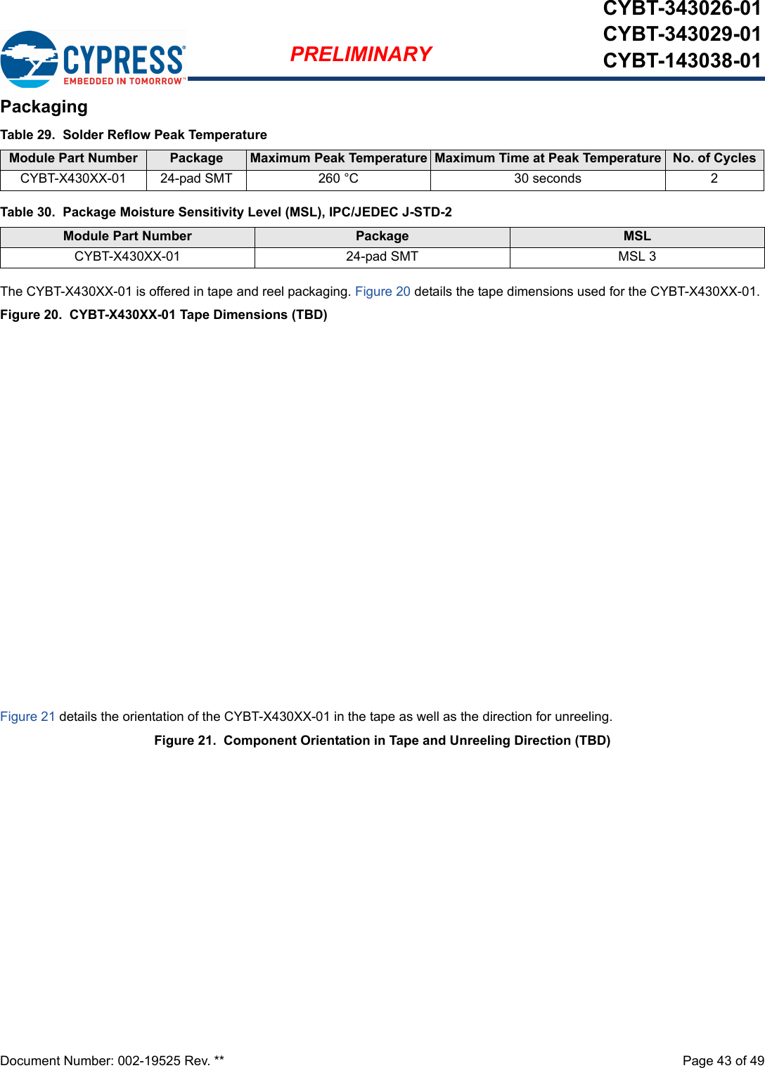
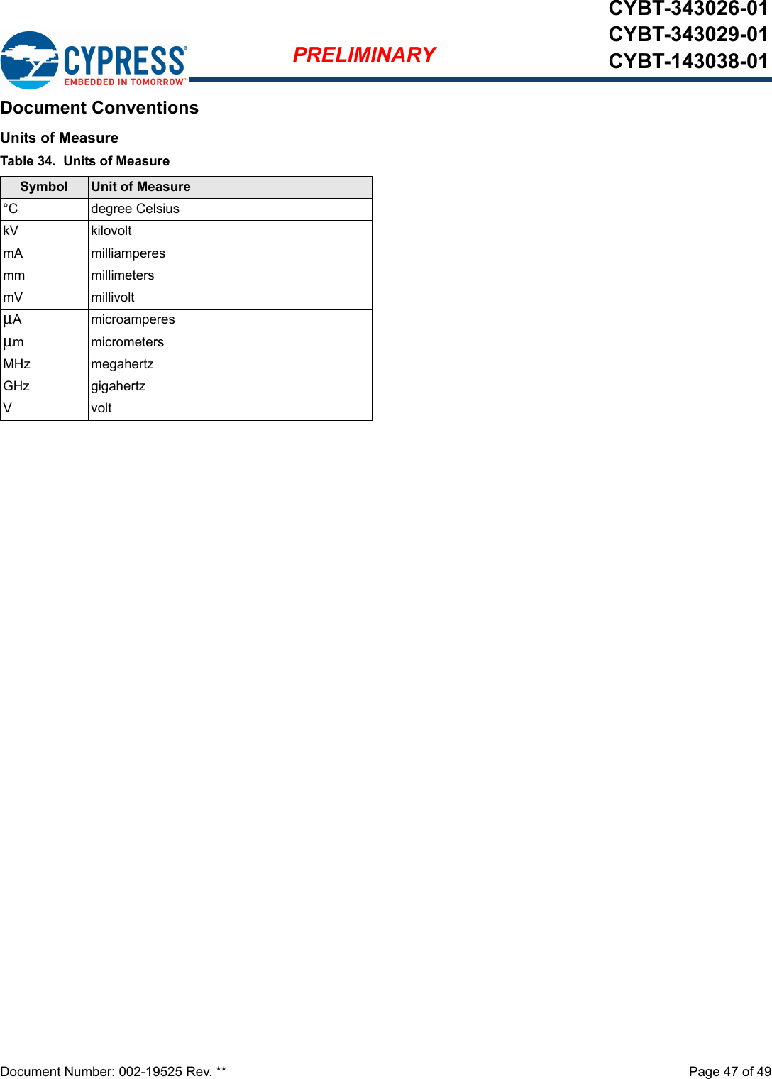
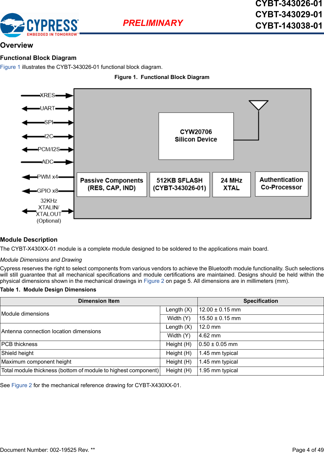
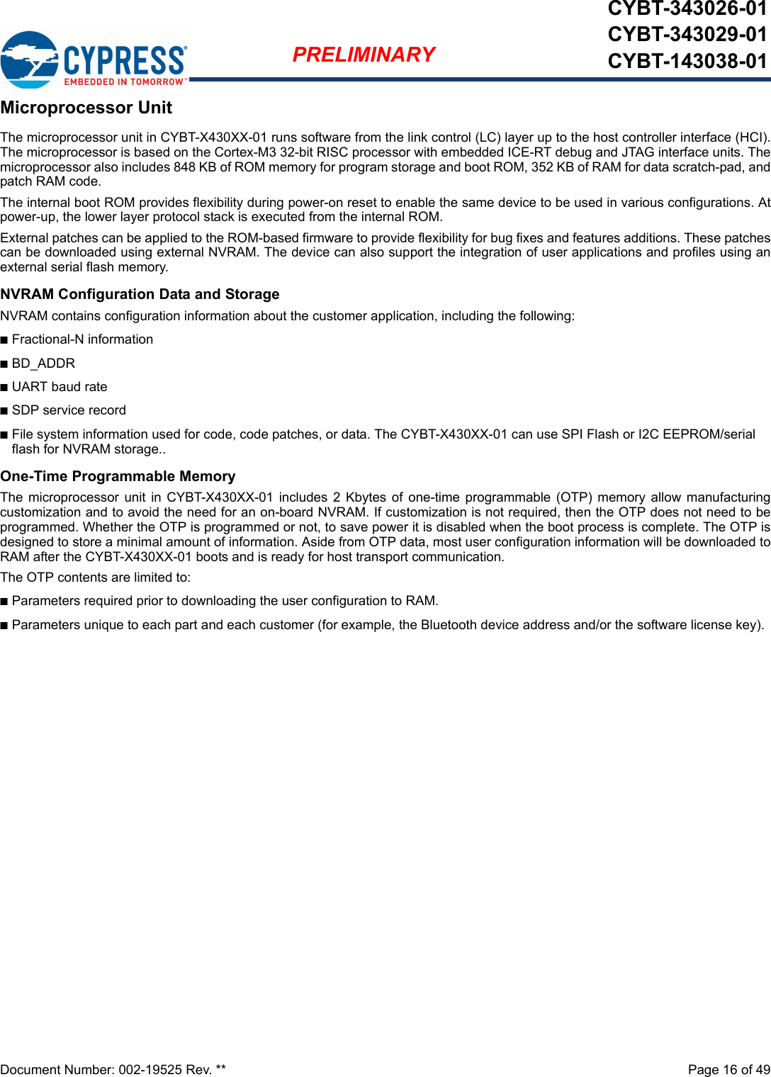
![Document Number: 002-19525 Rev. ** Page 39 of 49PRELIMINARYCYBT-343026-01CYBT-343029-01CYBT-143038-01Environmental SpecificationsEnvironmental ComplianceThis CYBT-X430XX-01 BLE module is produced in compliance with the Restriction of Hazardous Substances (RoHS) andHalogen-Free (HF) directives. The Cypress module and components used to produce this module are RoHS and HF compliant.RF CertificationThe CYBT-X430XX-01 module will be certified under the following RF certification standards at production release.nFCC: WAP3026nCEnIC: 7922A-3026nMIC: TBDSafety CertificationThe CYBT-X430XX-01 module complies with the following safety regulations:nUnderwriters Laboratories, Inc. (UL): Filing E331901nCSAnTUVEnvironmental ConditionsTab le 28 describes the operating and storage conditions for the Cypress BLE module.ESD and EMI ProtectionExposed components require special attention to ESD and electromagnetic interference (EMI).A grounded conductive layer inside the device enclosure is suggested for EMI and ESD performance. Any openings in the enclosurenear the module should be surrounded by a grounded conductive layer to provide ESD protection and a low-impedance path to ground. Device Handling: Proper ESD protocol must be followed in manufacturing to ensure component reliability.Table 28. Environmental Conditions for CYBT-X430XX-01Description Minimum Specification Maximum SpecificationOperating temperature −30 °C 85 °COperating humidity (relative, non-condensation) 5% 85%Thermal ramp rate – 3 °C/minuteStorage temperature –40 °C 85 °CStorage temperature and humidity – 85 °C at 85%ESD: Module integrated into system Components[4] –15 kV Air2.0 kV ContactNote4. This does not apply to the RF pins (ANT).](https://usermanual.wiki/Cypress-Semiconductor/3026.User-Manual/User-Guide-3461008-Page-39.png)