Cypress Semiconductor 3026 Bluetooth wireless EZ-BT Module User Manual CYBT 013033 01 EZ BT Module
Cypress Semiconductor Bluetooth wireless EZ-BT Module CYBT 013033 01 EZ BT Module
Contents
- 1. User Manual
- 2. User Guide
User Manual

PRELIMINARY
CYBT-343026-01
CYBT-343029-01
CYBT-143038-01
EZ-BT™ WICED Module
Cypress Semiconductor Corporation • 198 Champion Court • San Jose,CA 95134-1709 • 408-943-2600
Document Number: 002-19525 Rev. ** Revised May 31, 2017
General Description
The CYBT-X430XX-01 is a fully integrated Bluetooth Smart
Ready wireless module. The CYBT-X430XX-01 includes an
onboard crystal oscillator, passive components, flash memory,
and the Cypress CYW20706 silicon device. Refer to the
CYW20706 datasheet for additional details on the capabilities of
the silicon device used in this module.
The CYBT-X430XX-01 supports peripheral functions (ADC and
PWM), UART and USB communication, and a Bluetooth audio
interface. The CYBT-X430XX-01 includes a royalty-free BLE
stack compatible with Bluetooth 4.2 in a 12.0 × 15.5 × 1.95 mm
package.
The CYBT-343026-01 includes 512KB of onboard serial flash
memory and is designed for stand-alone opperation. The
CYBT-343029-01 has the same characterisitcs as the
CYBT-343026-01, but also include an on-board Apple
Authentication co-processor for use with Apple products such as
Homekit. The CYBT-143038-01 does not contain onboard flash,
requiring hosted control or application RAM upload operating
modes. The CYBT-143038-01 can also interface to external
flash on the host board. The CYBT-X430XX-01 utilizes an
integrated power amplifer to achieve Class I or Class II output
power capability.
The CYBT-X430XX-01 is fully qualified by Bluetooth SIG and is
targeted at applications requiring cost optimized BLE wireless
connectivity.
Module Description
nModule size: 12.00 mm × 15.50 mm × 1.95 mm
nBluetooth LE 4.2 Smart Ready module
pQDID: WAP3026
pDeclaration ID: 7922A-3026
nCertified to FCC, IC, MIC, and CE regulations
nCastelated solder pad connections for ease-of-use
n512-KB on-module serial flash memory ( CYBT-34302X-01)
nUp to 10 GPIOs
nTemperature range: –30 °C to +85 °C
nCortex-M3 32-bit processor
nMaximum TX output power:
p+12 dbm for Bluetooth EDR
p+9 dBm for Bluetooth Low Energy
nRX Receive Sensitivity:
p–93.5 dBm for Bluetooth Classic
p–96.5 dBm for Bluetooth Low Energy
Power Consumption[1]
nTX average current consumption: 12.5 mA (EDR) Class-II
nRX average current consumption: 20.0 mA (EDR)
nLow power mode support
pSleep: 120 uA
Functional Capabilities
n10-bit auxiliary ADC with nine analog channels
nSerial Communications interface compatible with I2C slaves
nSerial Peripheral Interface (SPI) support for both master and
slave modes
nHCI interface through USB or UART
nPCM/I2S Auido interface
n2-wire Global Coexistence Interface (GCI)
nBluetooth wideband speech support
nIntegrated peripherals such as PWM, ADC, Triac control
nProgrammable output power control
nMaximum of 100 LE Connections
nSupports extended synchronous connections (eSCO), for
enhanced voice quality by allowing for retransmission of
dropped packets
Benefits
CYBT-X430XX-01 provides all necessary components required
to operate BLE and/or EDR/BR communication standards.
nProven hardware design ready to use
nDual-mode operatoin eliminates the need for multiple modules
nCost optimized for applications without space constraints
nNon-volatile memory for self-sufficient operation and
Over-the-air updates ( CYBT-34302X-01 only)
nBluetooth SIG Listed with QDID and Declaration ID
nFully certified module eliminates the time needed for design,
development and certification processes
nWICED™ STUDIO 4.0 provides an easy-to-use integrated
design environment (IDE) to configure, develop, and program
a Bluetooth application
nPre-programmed EZ-Serial firmware platform to allow for
easy-to-use out of the box Bluetooth connectivity
Notes
1. The values in this section were calculated for a 90% efficient DC-DC at 3V in HCI mode, and based on a Class I configurationbench-marked at Class II. Lower values
are expected for a class II configuration using an external LPO and corresponding PAconfiguration

Document Number: 002-19525 Rev. ** Page 2 of 49
PRELIMINARY
CYBT-343026-01
CYBT-343029-01
CYBT-143038-01
More Information
Cypress provides a wealth of data at www.cypress.com to help you to select the right module for your design, and to help you to
quickly and effectively integrate the module into your design.
References
nOverview: EZ-BLE/BT Module Portfolio, Module Roadmap
nEZ-BT WICED Product Overview
nCYW20706 BT Silicon Datasheet
nKnowledge Base Article
pKBA97095 - EZ-BLE™ Module Placement
pKBA213260 - RF Regulatory Certifications for
CYBT-343026-01 and CYBT-143038-01 EZ-BT™ WICED
Modules
pKBA213976 - FAQ for BLE and Regulatory Certifications with
EZ-BLE modules
pKBA210802 - Queries on BLE Qualification and Declaration
Processes
nDevelopment Kits:
pCYBT-343026-EVAL, CYBT-343026-01 Evaluation Board
nTest and Debug Tools:
pCYSmart, Bluetooth® LE Test and Debug Tool (Windows)
pCYSmart Mobile, Bluetooth® LE Test and Debug Tool
(Android/iOS Mobile App)
Development Environments
Two Easy-To-Use Design Environments to Get You Started Quickly
Wireless Connectivity for Embedded Devices (WICED) Studio Software Development Kit (SDK)
Cypress's WICED® (Wireless Connectivity for Embedded Devices) is a full-featured platform with proven Software Development Kits
(SDKs) and turnkey hardware solutions from partners to readily enable Wi-Fi and Bluetooth® connectivity in system design.
WICED Studio is the only SDK for the Internet of Things (ioT) that combines Wi-Fi and Bluetooth into a single integrated development
environment. In addition to providing WICED APIs and an application framework designed to abstract complexity, WICED Studio also
leverages many common industry standards.
EZ-Serial™ BT Firmware Platform
Cypress’s EZ-Serial Firmware Platform provides a simple way to access the most common hardware and communication features
needed in Bluetooth applications. EZ-Serial implements an intuitive API protocol over the UART interface and exposes various status
and control signals through the module’s GPIOs, making it easy to add BLE and/or EDR/BR functionality quickly to existing designs.
Use a simple serial terminal and evaluation kit to begin development without requiring an IDE.
EZ-BT modules with non-volatile memory are pre-flashed with the EZ-Serial Firmware Platform. If you do not have EZ-Serial
pre-loaded on your module, you can download each EZ-BT module’s firmware images on the EZ-Serial webpage.
Technical Support
nCypress Community: Whether you’re a customer, partner or a developer interested in the latest Cypress innovations, the Cypress
Developer Community offers you a place to learn, share and engage with both Cypress experts and other embedded engineers
around the world.
nFrequently Asked Questions (FAQs): Learn more about our BLE ECO System.
nVisit our support page and create a technical support case or contact a local sales representatives. If you are in the United States,
you can talk to our technical support team by calling our toll-free number: +1-800-541-4736. Select option 2 at the prompt.

Document Number: 002-19525 Rev. ** Page 3 of 49
PRELIMINARY
CYBT-343026-01
CYBT-343029-01
CYBT-143038-01
Contents
Overview............................................................................ 4
Functional Block Diagram ........................................... 4
Module Description...................................................... 4
Pad Connection Interface ................................................ 6
Recommended Host PCB Layout ................................... 7
Module Connections ........................................................ 9
Connections and Optional External Components....... 11
Power Connections (VDDIN)..................................... 11
External Reset (XRES).............................................. 11
Multiple-Bonded GPIO Connections ......................... 11
Using CYBT-143038-01 with External Flash............. 11
Critical Components List ........................................... 13
Antenna Design......................................................... 13
Bluetooth Baseband Core ............................................. 14
Link Control Layer ..................................................... 14
Test Mode Support.................................................... 15
Frequency Hopping Generator.................................. 15
Microprocessor Unit....................................................... 16
NVRAM Configuration Data and Storage.................. 16
One-Time Programmable Memory............................ 16
External Reset (XRES).............................................. 17
Integrated Radio Transceiver ........................................ 18
Transmitter Path........................................................ 18
Digital Modulator ....................................................... 18
Digital Demodulator and Bit Synchronizer................. 18
Power Amplifier ......................................................... 18
Receiver Path............................................................ 18
Digital Demodulator and Bit Synchronizer................. 18
Receiver Signal Strength Indicator............................ 18
Local Oscillator Generation....................................... 18
Calibration ................................................................. 18
Internal LDO .............................................................. 19
Collaborative Coexistence............................................. 19
Global Coexistence Interface ........................................ 19
SECI I/O .................................................................... 19
Peripheral Transport Unit .............................................. 19
Cypress Serial Communications Interface ................ 19
UART Interface.......................................................... 20
Peripheral UART Interface ........................................ 21
PCM Interface.................................................................. 21
Slot Mapping ............................................................. 21
Frame Synchronization ............................................. 21
Data Formatting......................................................... 21
Burst PCM Mode....................................................... 21
Clock Frequencies.......................................................... 21
GPIO Port ........................................................................ 22
PWM................................................................................. 22
Triac Control/PWM ......................................................... 23
Serial Peripheral Interface ............................................. 23
Power Management Unit................................................ 23
RF Power Management ............................................ 23
Host Controller Power Management ......................... 24
BBC Power Management.......................................... 24
Electrical Characteristics............................................... 25
RF Specifications ........................................................... 27
Timing and AC Characteristics ..................................... 30
UART Timing............................................................. 30
SPI Timing................................................................. 31
BSC Interface Timing ................................................ 33
PCM Interface Timing................................................ 34
I2S Interface Timing .................................................. 38
Environmental Specifications ....................................... 39
Environmental Compliance ....................................... 39
RF Certification.......................................................... 39
Safety Certification .................................................... 39
Environmental Conditions ......................................... 39
ESD and EMI Protection ........................................... 39
Regulatory Information .................................................. 40
FCC........................................................................... 40
ISED.......................................................................... 41
European Declaration of Conformity ......................... 42
MIC Japan................................................................. 42
Packaging........................................................................ 43
Ordering Information...................................................... 45
Acronyms........................................................................ 46
Document Conventions ................................................. 47
Units of Measure ....................................................... 47
Document History Page ................................................. 48
Sales, Solutions, and Legal Information ...................... 49
Worldwide Sales and Design Support....................... 49
Products .................................................................... 49
PSoC® Solutions ...................................................... 49
Cypress Developer Community................................. 49
Technical Support ..................................................... 49
Document Number: 002-19525 Rev. ** Page 4 of 49
PRELIMINARY
CYBT-343026-01
CYBT-343029-01
CYBT-143038-01
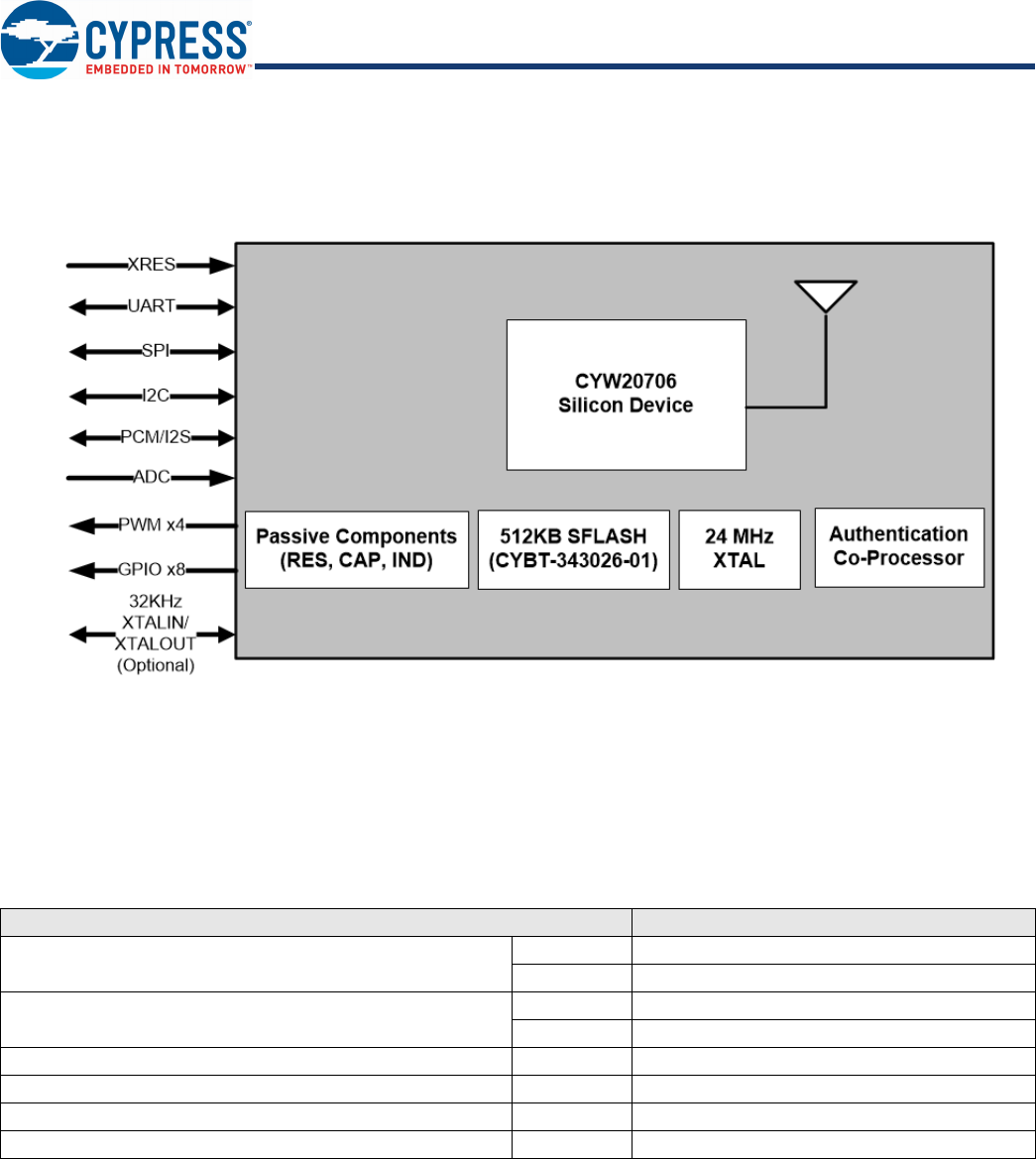
Overview
Functional Block Diagram
Figure 1 illustrates the CYBT-343026-01 functional block diagram.
Figure 1. Functional Block Diagram
Module Description
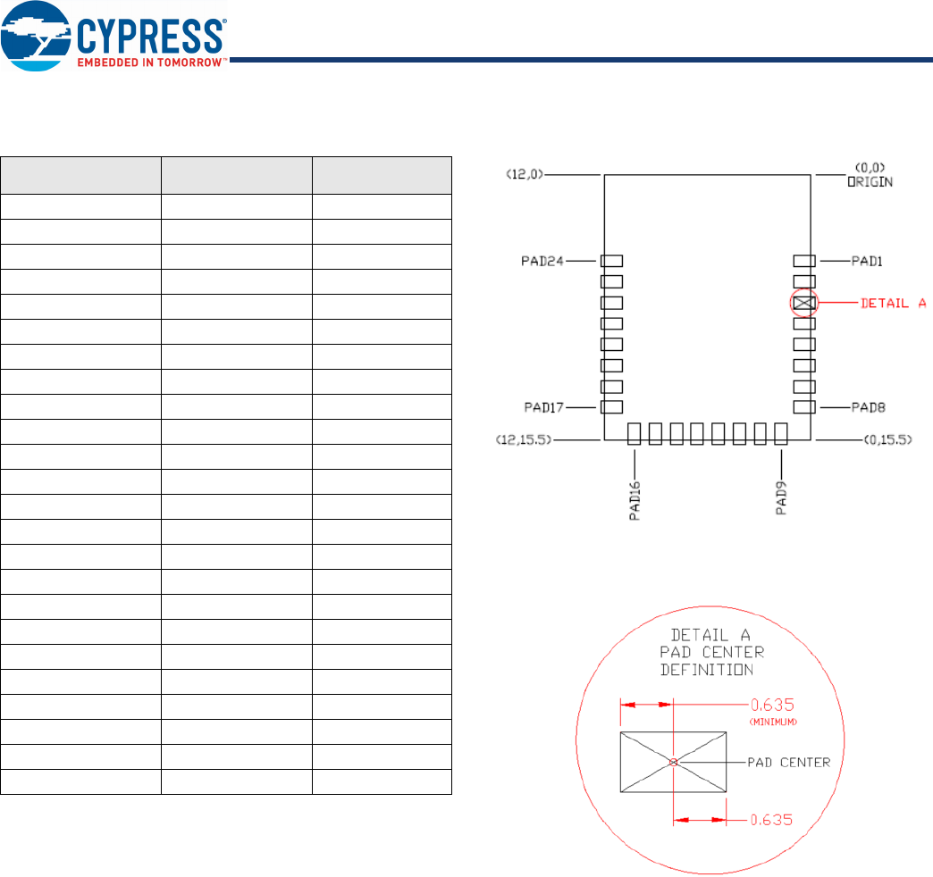
The CYBT-X430XX-01 module is a complete module designed to be soldered to the applications main board.
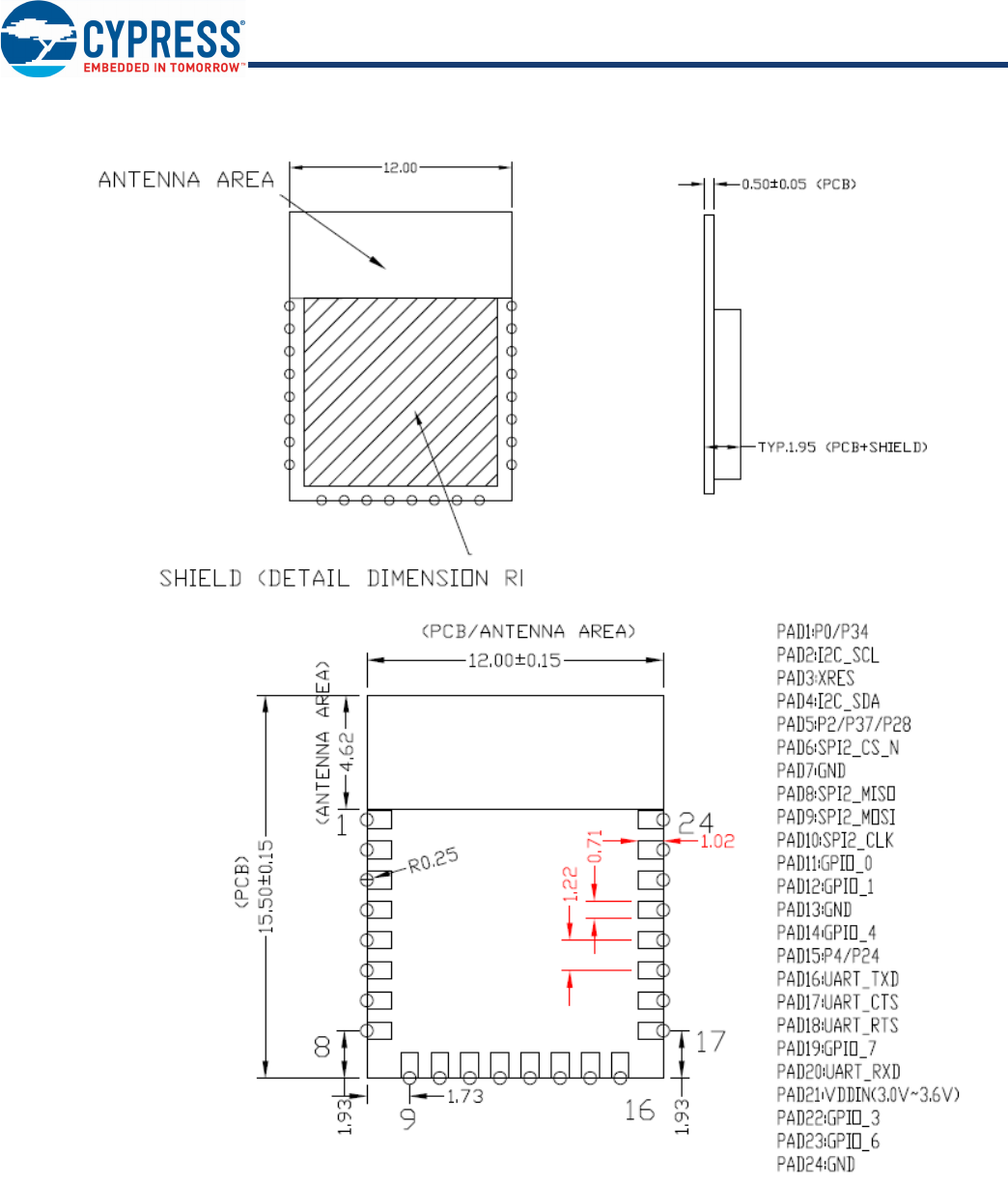
Module Dimensions and Drawing
Cypress reserves the right to select components from various vendors to achieve the Bluetooth module functionality. Such selections
will still guarantee that all mechanical specifications and module certifications are maintained. Designs should be held within the
physical dimensions shown in the mechanical drawings in Figure 2 on page 5. All dimensions are in millimeters (mm).
Table 1. Module Design Dimensions
See Figure 2 for the mechanical reference drawing for CYBT-X430XX-01.
Dimension Item Specification
Module dimensions Length (X) 12.00 ± 0.15 mm
Width (Y) 15.50 ± 0.15 mm
Antenna connection location dimensions Length (X) 12.0 mm
Width (Y) 4.62 mm
PCB thickness Height (H) 0.50 ± 0.05 mm
Shield height Height (H) 1.45 mm typical
Maximum component height Height (H) 1.45 mm typical
Total module thickness (bottom of module to highest component) Height (H) 1.95 mm typical
Document Number: 002-19525 Rev. ** Page 5 of 49
PRELIMINARY
CYBT-343026-01
CYBT-343029-01
CYBT-143038-01
Figure 2. Module Mechanical Drawing
Bottom View (Seen from Bottom)
Side View
Top View (See
Notes
2. No metal should be located beneath or above the antenna area. Only bare PCB material should be located beneath the antenna area. For more information on
recommended host PCB layout, see “Recommended Host PCB Layout” on page 7.
3. The CYBT-343026-01 includes castellated pad connections, denoted as the circular openings at the pad location above.
Document Number: 002-19525 Rev. ** Page 6 of 49
PRELIMINARY
CYBT-343026-01
CYBT-343029-01
CYBT-143038-01
Pad Connection Interface
As shown in the bottom view of Figure 2 on page 5, the CYBT-X430XX-01 connects to the host board via solder pads on the backside
of the module. Tab le 2 and Figure 3 detail the solder pad length, width, and pitch dimensions of the CYBT-X430XX-01 module.
Figure 3. Solder Pad Dimensions (Seen from Bottom
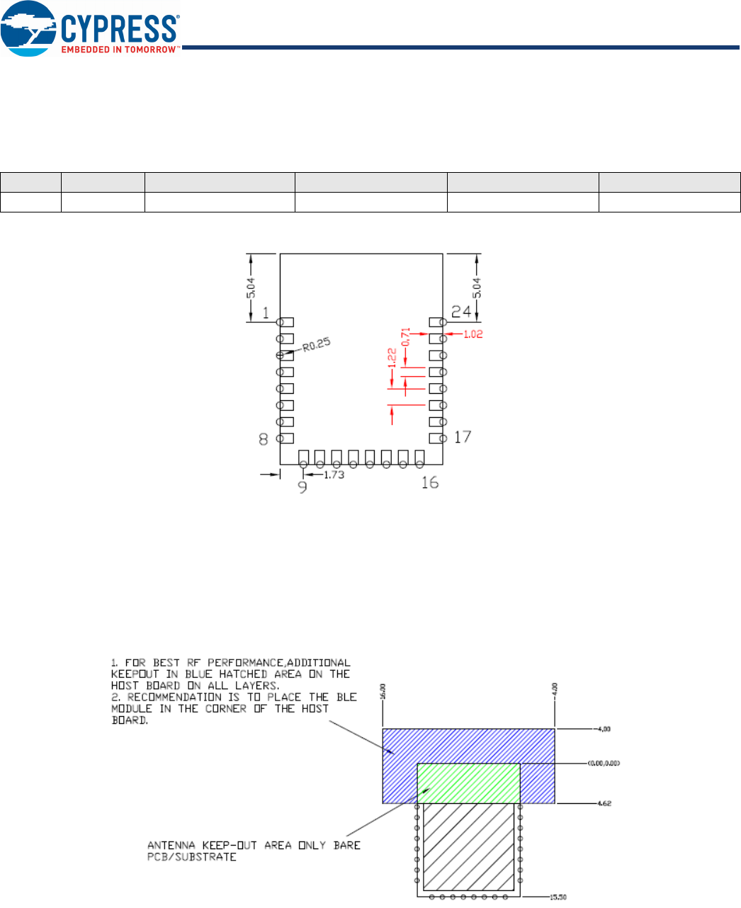
To maximize RF performance, the host layout should follow these recommendations:
1. Antenna Area Keepout: The host board directly below the antenna area of the Cypress module (see Figure 2 on page 5) must
contain no ground or signal traces. This keep out area requirement applies to all layers of the host board.
2. Module Placement: The ideal placement of the Cypress Bluetooth module is in a corner of the host board with the PCB trace
antenna located at the far corner. This placement minimizes the additional recommended keep out area stated in item 2. Please
refer to AN96841 for module placement best practices.
Figure 4. Recommended Host PCB Keep Out Area Around the CYBT-X430XX-01 Antenna
Table 2. Connection Description
Name Connections Connection Type Pad Length Dimension Pad Width Dimension Pad Pitch
SP 24 Solder Pads 1.02 mm 0.71 mm 1.27 mm
Document Number: 002-19525 Rev. ** Page 7 of 49
PRELIMINARY
CYBT-343026-01
CYBT-343029-01
CYBT-143038-01
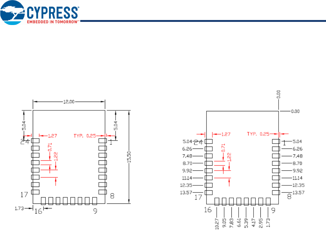
Recommended Host PCB Layout
Figure 5, Figure 6, Figure 7, and Tab le 3 provide details that can be used for the recommended host PCB layout pattern for the
CYBT-X430XX-01. Dimensions are in millimeters unless otherwise noted. Pad length of 1.27 mm (0.635 mm from center of the pad
on either side) shown in Figure 7 is the minimum recommended host pad length. The host PCB layout pattern can be completed using
either Figure 5, Figure 6, or Figure 7. It is not necessary to use all figures to complete the host PCB layout pattern.
Figure 5. CYBT-X430XX-01 Host Layout (Dimensioned) Figure 6. CYBT-X430XX-01 Host Layout (Relative to Origin)
Top View (Seen on Host PCB)
Top View (Seen on Host PCB)
Document Number: 002-19525 Rev. ** Page 8 of 49
PRELIMINARY
CYBT-343026-01
CYBT-343029-01
CYBT-143038-01
Tab le 3 provides the center location for each solder pad on the CYBT-X430XX-01. All dimensions reference the to the center of the
solder pad. Refer to Figure 6 for the location of each module solder pad.
Table 3. Module Solder Pad Location Figure 7. Solder Pad Reference Location
Solder Pad
(Center of Pad)
Location (X,Y) from
Orign (mm)
Dimension from
Orign (mils)
1 (0.38, 5.04) (14.96, 198.42)
2 (0.38, 6.26) (14.96, 246.46)
3 (0.38, 7.48) (14.96, 294.49)
4 (0.38, 8.70) (14.96, 342.52)
5 (0.38, 9.92) (14.96, 390.55)
6 (0.38, 11.14) (14.96, 438.58)
7 (0.38, 12.35) (14.96, 486.22)
8 (0.38, 13.57) (14.96, 534.25)
9 (1.73, 15.11) (68.11, 594.88)
10 (2.95, 15.11) (116.14, 594.88)
11 (4.17, 15.11) (164.17, 594.88)
12 (5.39, 15.11) (212.20, 594.88)
13 (6.61, 15.11) (260.24, 594.88)
14 (7.83, 15.11) (308.27, 594.88)
15 (9.05, 15.11) (356.30, 594.88)
16 (10.27, 15.11) (404.33, 594.88)
17 (11.62, 13.57) (457.48, 534.25)
18 (11.62, 12.35) (457.48, 486.22)
19 (11.62, 11.14) (457.48, 438.58)
20 (11.62, 9.92) (457.48, 390.55)
21 (11.62, 8.70) (457.48, 342.52)
22 (11.62, 7.48) (457.48, 294.49)
23 (11.62, 6.26) (457.48, 246.46)
24 (11.62, 5.04) (457.48, 198.42)
Top View (Seen on Host PCB)
Document Number: 002-19525 Rev. ** Page 9 of 49
PRELIMINARY
CYBT-343026-01
CYBT-343029-01
CYBT-143038-01
Module Connections
Tab le 4 and Table 5 detail the solder pad connection definitions and available functions for the pad connections for the
CYBT-34302X-01 and CYBT-143038-01 respectively. Tabl e 4 and Table 5 lists the solder pads on the CYBT-X430XX-01 modules,
the silicon device pin, and denotes what functions are available for each solder pad. The CYBT-343026-01 and CYBT-343029-01
share a common footprint.
Table 4. CYBT-343026-01 and CYBT-343029-01 Solder Pad Connection Definitions
Pad Pad Name UART SPI1
1. The CYBT-343026-01 contains a single SPI (SPI1) peripheral supporting both master or slave configurations. SPI2 is used for on-module serial memory interface.
I2C ADC QD2
2. Quadrature Decoder
CLK/XTAL GPIO Other
1P0/P34
PUART_TX/P0
PUART_RX/P34 SPI1_MOSI/P0
(master/slave) IN29/P0
IN5/P34 DY0/P34 3PCM_Sync
I2S_WS
2 I2C_SCL SCL
3 XRES External Reset (Active Low)
4 I2C_SDA SDA
5 P2/P37/P28 PUART_RX/P2 SPI1_CS(slave)/P2
SPI1_MOSI(master)/P2
SPI1_MISO(slave)/P37 SCL/P37 IN11/P28
IN2/P37
DX0/P2
OC2/P28
DZ1/P37 ACK1/P37 3
6 SPI2_CS_N No Connect (Used for on-module memory SPI interface for CYBT-343026-01)
7 GND Ground
8 SPI2_MISO No Connect (Used for on-module memory SPI interface for CYBT-343026-01)
9 SPI2_MOSI No Connect (Used for on-module memory SPI interface for CYBT-343026-01)
10 SPI2_CLK No Connect (Used for on-module memory SPI interface for CYBT-343026-01)
11 GPIO_0 SPI1_CLK/P36
SPI1_MOSI/P38
(master/slave)
IN3/P36
IN1/P38 DZ0/P36 ACLK0/P36
3
(DevWake
)
~TX_PD/P36
12 GPIO_1 PUART_RX/P25
PUART_TX/P32
SPI1_MISO/P25
(master/slave)
SPI1_CS/P32
(slave)
IN7/P32 DX0/P32 ACLK0/P32
3
(HostWak
e)
13 GND Ground
14 GPIO_4 PUART_RTS/P6
PUART_TX/P31 SPI1_CS/P6
(slave) IN8/P31 DZ0/P6 3
(GCI) Ext LPO In
15 P4/P24 PUART_RX/P4
PUART_TX/P24
SPI1_MOSI/P6
(master/slave)
SPI1_CLK/P24
(master/slave)
DY0/P4 3
(CLK_RE
Q)
16 UART_TXD UART Transmit Data
17 UART_CTS UART Clear To Send Input
18 UART_RTS UART Request To Send Output
19 GPIO_7 PUART_RTS/P30 IN9/P30 3
(GCI)
20 UART_RXD UART Receive Data
21 VDDIN VDDIN (3.0V ~ 3.6V)
22 GPIO_3 UART_RX/P33
SPI1_MOSI/P27
(master/slave)
SPI1_MOSI/P33
(slave)
IN6/P33 OC1/P27
DX1/P33 ACLK1/P33 3
PWM2/P27
23 GPIO_6 SPI1_CS/P26
(slave) IN24/P11 OC0/P26 3
(GCI) PWM1/P26
24 GND Ground
Document Number: 002-19525 Rev. ** Page 10 of 49
PRELIMINARY
CYBT-343026-01
CYBT-343029-01
CYBT-143038-01
Table 5. CYBT-143038-01 Solder Pad
Pad Pad Name UART SPI1
1. The CYBT-143038-01 contains two SPI peripherals, SPI1 and SPI2. SPI1 supports only master or slave modes, whereas SPI2 supports master only mode. The con-
nections shown in Table 5 above detail the SPI function for the given mode shown in parenthesis. If external memory is used with the CYBT-143038-01, then SPI2
should be used as the interface.
I2C ADC QD2
2. Quadrature Decoder
CLK/XTAL GPIO Other
1P0/P34
PUART_TX/P0
PUART_RX/P34 SPI1_MOSI/P0
(master/slave) IN29/P0
IN5/P34 DY0/P34 3PCM_Sync
I2S_WS
2 I2C_SCL SCL
3XRES External reset
4 I2C_SDA SDA
5 P2/P37/P28 PUART_RX/P2
SPI1_CS(slave)/P2
SPI1_MOSI(master)/
P2
SPI1_MISO(slave)/P3
7
SCL/P37 IN11/P28
IN2/P37
DX0/P2
OC2/P28
DZ1/P37 ACK1/P37 3
6 SPI2_CS_N SPI2 active-low chip
select
7 GND Ground
8 SPI2_MISO SPI2_MISO
(master) SCL
9 SPI2_MOSI SPI2_MOSI
(master) SDA
10 SPI2_CLK SPI2_CLK
(master)
11 GPIO_0 SPI1_CLK/P36
SPI1_MOSI/P38
(master/slave)
IN3/P36
IN1/P38 DZ0/P36 ACLK0/P36 3
(DevWake)
~TX_PD/P36
12 GPIO_1 PUART_RX/P25
PUART_TX/P32
SPI1_MISO/P25
(master/slave)
SPI1_CS/P32
(slave)
IN7/P32 DX0/P32 ACLK0/P32 3
(Host Wake)
13 GND Ground
14 GPIO_4 PUART_RTS/P6
PUART_TX/P31 SPI1_CS/P6
(slave) IN8/P31 DZ0/P6 3
(GCI) Ext LPO In
15 P4/P24 PUART_RX/P4
PUART_TX/P24
SPI1_MOSI/P6
(master/slave)
SPI1_CLK/P24
(master/slave)
DY0/P4 3
(CLK_REQ)
16 UART_TXD UART transmit data
17 UART_CTS UART clear to send input
18 UART_RTS UART request to send output
19 GPIO_7 PUART_RTS/P30 IN9/P30 3
(GCI)
20 UART_RXD UART receive data
21 VDDIN VDDIN (3.0V ~ 3.6V)
22 GPIO_3 UART_RX/P33
SPI1_MOSI/P27
(master/slave)
SPI1_MOSI/P33
(slave)
IN6/P33 OC1/P27
DX1/P33 ACLK1/P33 3
PWM2/P27
23 GPIO_6 SPI1_CS/P26
(slave) IN24/P11 OC0/P26 3
(GCI) PWM1/P26
24 GND Ground

Document Number: 002-19525 Rev. ** Page 11 of 49
PRELIMINARY
CYBT-343026-01
CYBT-343029-01
CYBT-143038-01
Connections and Optional External Components
Power Connections (VDDIN)
The CYBT-X430XX-01 contains one power supply connection, VDDIN. VDDIN accepts a supply input range of 2.3 V to 3.6 V for
CYBT-34302X-01 and 1.62 V to 3.6 V for the CYBT-143038-01. Tabl e 1 2 provides this specification. The maximum power supply
ripple for this power connection is 100 mV, as shown in Tab le 12.
It is not required to place any power supply decoupling or noise reduction circuitry on the host PCB. If desired, an external ferrite bead
between the supply and the module connection can be included, but is not necessary. If used, the ferrite bead should be positioned
as close as possible to the module pin connection and the recommended ferrite bead value is 330Ω, 100 MHz.
External Reset (XRES)
The CYBT-X430XX-01 has an integrated power-on reset circuit which completely resets all circuits to a known power on state. This
action can also be envoked by an external reset signal, forcing it into a power-on reset state. The XRES signal is an active-low signal,
which is an input to the CYBT-X430XX-01 module (solder pad 3). The CYBT-X430XX-01 module does not require an external pull-up
resistor on the XRES input
During power on operation, the XRES connection to the CYBT-X430XX-01 is required to be held low 50 ms after the VDD power
supply input to the module is stable. This can be accomplished in the following ways:
nThe host device should connect a GPIO to the XRES of Cypress CYBT-X430XX-01 module and pull XRES low until VDD is stable.
XRES is recommended to be released 50 ms after VDDIN is stable.
nThe XRES release timing may be controlled by a external voltage detection circuit. XRES should be released 50 ms after VDD is
stable.
Refer to Figure 10 on page 17 for XRES operating and timing requirements during power on events.
Multiple-Bonded GPIO Connections
The CYBT-X430XX-01 contains GPIO which are multiple-bonded at the silicon level. If any of these dual-bonded GPIO are used, only
the functionality and features for one of these port pins may be used. The desired port pin should be configured in the WICED Studio
SDK. For details on the features and functions that each of these multiple-bonded GPIO provide, please refer to Table 4 and Table 5.
Using CYBT-143038-01 with External Flash
The CYBT-143038-01 does not contain any on-module non-volatile memory. If desired, the CYBT-143038-01 can be used with an
external memory device (SFLASH).
If EEPROM is used as an external memory device with I2C interface, module solder pads 4 (SDA) and 2 (SCL) must be used as the
I2C interface.
If using external SFLASH as the memory interface, SPI2 (master) must be used as the interface to the SFLASH device. The specific
GPIO required and the applicable SPI signal is shown below. These are the same signals used for SFLASH interface on the
CYBT-343026-01.
1. SPI signal MOSI: Module Solder Pad 9, silicon connection SPI2_MOSI_I2C_SDA
2. SPI signal MISO: Module Solder Pad 8, silicon connection SPI2_MISO_I2C_SCL
3. SPI Signal CLK: Module Solder Pad 10 silicon connection SPI2_CLK
4. SPI Signal CS: Module Solder Pad 6, silicon connection SPI2_CSN
Document Number: 002-19525 Rev. ** Page 13 of 49
PRELIMINARY
CYBT-343026-01
CYBT-343029-01
CYBT-143038-01
Critical Components List
Tab le 6 details the critical components used in the CYBT-X430XX-01 module.
Table 6. Critical Component List
Antenna Design
Tab le 7 details trace antenna used in the CYBT-X430XX-01 module. For more information, see Tab le 7.
Table 7. Trace Antenna Specifications
Component Reference Designator Description
Silicon U1 49-pin FBGA BT/BLE Silicon Device - CYW20706
Silicon U2 8-pin TDF8N, 512KSerial Flash ( CYBT-34302X-01)
Crystal Y1 24.000 MHz, 12PF
Item Description
Frequency Range 2400 – 2500 MHz
Peak Gain –0.5 dBi typical
Return Loss 10 dB minimum

Document Number: 002-19525 Rev. ** Page 14 of 49
PRELIMINARY
CYBT-343026-01
CYBT-343029-01
CYBT-143038-01
Bluetooth Baseband Core
The Bluetooth Baseband Core (BBC) implements all of the time-critical functions required for high-performance Bluetooth operation.
The BBC manages the buffering, segmentation, and routing of data for all connections. It also buffers data that passes through it,
handles data flow control, schedules SCO/ACL and TX/RX transactions, monitors Bluetooth slot usage, optimally segments and
packages data into baseband packets, manages connection status indicators, and composes and decodes HCI packets. In addition
to these functions, it independently handles HCI event types, and HCI command types. The following transmit and receive functions
are also implemented in the BBC hardware to increase reliability and security of the TX/RX data before sending over the air:
nSymbol timing recovery, data deframing, forward error correction (FEC), header error control (HEC), cyclic redundancy check (CRC),
data decryption, and data dewhitening in the receiver.
nData framing, FEC generation, HEC generation, CRC generation, key generation, data encryption, and data whitening in the
transmitter.
Bluetooth 4.2 Features
CYBT-X430XX-01 supports all Bluetooth 4.2 and legacy features, with the following benefits
nDual-mode Bluetooth (BT and BLE operation)
nExtended inquiry response (EIR): Shortens the time to retrieve the device name, specific profile, and operating mode.
nEncryption pause resume (EPR): Enables the use of Bluetooth technology in a much more secure environment.
nSniff subrating (SSR): Optimizes power consumption for low duty cycle asymmetric data flow, which subsequently extends battery life.
nSecure simple pairing (SSP): Reduces the number of steps for connecting two devices, with minimal or no user interaction required.
nLink supervision time out (LSTO): Additional commands added to HCI and Link Management Protocol (LMP) for improved link
timeout supervision.
nQuality of service (QoS) enhancements: Changes to data traffic control, which results in better link performance. Audio, human
interface device (HID), bulk traffic, SCO, and enhanced SCO (eSCO) are improved with the erroneous data (ED) and packet boundary
flag (PBF) enhancements.
nSecure connections (BR/EDR)
nFast advertising interval
nPiconet clock adjust
nConnectionless broadcast
nLE privacy v1.1
nLow duty cycle directed advertising
nLE dual mode topology
Link Control Layer
The link control layer is part of the Bluetooth link control functions that are implemented in dedicated logic in the link control unit (LCU).
This layer consists of the command controller that takes commands from the software, and other controllers that are activated or
configured by the command controller, to perform the link control tasks. Each task is performed in a different state in the Bluetooth
Link Controller.
nStates:
pStandby
pConnection
pPage
pPage Scan
pInquiry
pInquiry Scan
pSniff
pAdvertising
pScanning

Document Number: 002-19525 Rev. ** Page 15 of 49
PRELIMINARY
CYBT-343026-01
CYBT-343029-01
CYBT-143038-01
Test Mode Support
The CYBT-X430XX-01 fully supports Bluetooth Test mode as described in Part I:1 of the Specification of the Bluetooth System Version
3.0.
This includes the transmitter tests, normal and delayed loopback tests, and reduced hopping sequence.
In addition to the standard Bluetooth Test Mode, the CYBT-X430XX-01also supports enhanced testing features to simplify RF
debugging and qualification and type-approval testing. These features include:
nFixed frequency carrier wave (unmodulated) transmission
pSimplifies some type-approval measurements (Japan)
pAids in transmitter performance analysis
nFixed frequency constant receiver mode
pReceiver output directed to I/O pin
pAllows for direct BER measurements using standard RF test equipment
pFacilitates spurious emissions testing for receive mode
nFixed frequency constant transmission
p8-bit fixed pattern or PRBS-9
pEnables modulated signal measurements with standard RF test equipment.
Frequency Hopping Generator
The frequency hopping sequence generator selects the correct hopping channel number based on the link controller state, Bluetooth
clock, and device address.

Document Number: 002-19525 Rev. ** Page 16 of 49
PRELIMINARY
CYBT-343026-01
CYBT-343029-01
CYBT-143038-01
Microprocessor Unit
The microprocessor unit in CYBT-X430XX-01 runs software from the link control (LC) layer up to the host controller interface (HCI).
The microprocessor is based on the Cortex-M3 32-bit RISC processor with embedded ICE-RT debug and JTAG interface units. The
microprocessor also includes 848 KB of ROM memory for program storage and boot ROM, 352 KB of RAM for data scratch-pad, and
patch RAM code.
The internal boot ROM provides flexibility during power-on reset to enable the same device to be used in various configurations. At
power-up, the lower layer protocol stack is executed from the internal ROM.
External patches can be applied to the ROM-based firmware to provide flexibility for bug fixes and features additions. These patches
can be downloaded using external NVRAM. The device can also support the integration of user applications and profiles using an
external serial flash memory.
NVRAM Configuration Data and Storage
NVRAM contains configuration information about the customer application, including the following:
nFractional-N information
nBD_ADDR
nUART baud rate
nSDP service record
nFile system information used for code, code patches, or data. The CYBT-X430XX-01 can use SPI Flash or I2C EEPROM/serial
flash for NVRAM storage..
One-Time Programmable Memory
The microprocessor unit in CYBT-X430XX-01 includes 2 Kbytes of one-time programmable (OTP) memory allow manufacturing
customization and to avoid the need for an on-board NVRAM. If customization is not required, then the OTP does not need to be
programmed. Whether the OTP is programmed or not, to save power it is disabled when the boot process is complete. The OTP is
designed to store a minimal amount of information. Aside from OTP data, most user configuration information will be downloaded to
RAM after the CYBT-X430XX-01 boots and is ready for host transport communication.
The OTP contents are limited to:
nParameters required prior to downloading the user configuration to RAM.
nParameters unique to each part and each customer (for example, the Bluetooth device address and/or the software license key).
Document Number: 002-19525 Rev. ** Page 17 of 49
PRELIMINARY
CYBT-343026-01
CYBT-343029-01
CYBT-143038-01
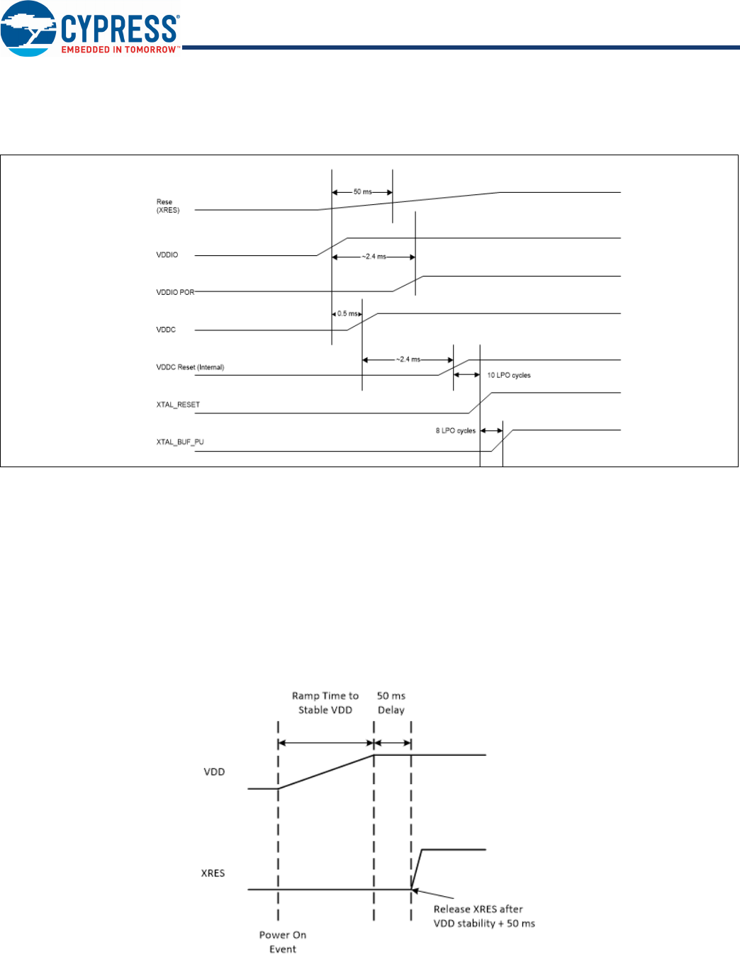
External Reset (XRES)
The CYBT-X430XX-01 has an integrated power-on reset circuit that completely resets all circuits to a known power-on state. An
external active low reset signal, XRES, can be used to put the CYBT-X430XX-01 in the reset state. The XRES pin has an internal
pull-up resistor and, in most applications, it does not require that anything be connected to it.
Figure 9. External Reset Internal Timing
External Reset (XRES) Recommended External Components and Proper Operation
During a power on event, the XRES line of the CYBT-X430XX-01 is required to be held low 50 ms after the VDD power supply input
to the module is stable. Refer to Figure 10 for the Power On XRES timing operation. This power on operation can be accomplished
in the following ways:
nA host device should connect a GPIO to the XRES of Cypress CYBT-X430XX-01 module and pull XRES low until VDD is stable.
XRES can be released after VDD is stable.
nIf the XRES connection of the CYBT-X430XX-01 module is not used in the application, a 0.47uF capacitor may be connected to the
XRES solder pad of the CYBT-X430XX-01.
nThe XRES release timing can also be controlled via a external voltage detection circuit.
Figure 10. Power On External Reset (XRES) Operation

Document Number: 002-19525 Rev. ** Page 18 of 49
PRELIMINARY
CYBT-343026-01
CYBT-343029-01
CYBT-143038-01
Integrated Radio Transceiver
The CYBT-X430XX-01 has an integrated radio transceiver that has been optimized for use in 2.4 GHz Bluetooth wireless systems. It
has been designed to provide low-power, low-cost, robust communications for applications operating in the globally available 2.4 GHz
unlicensed ISM band. The CYBT-X430XX-01 is fully compliant with the Bluetooth Radio Specification and enhanced data rate (EDR)
specification and meets or exceeds the requirements to provide the highest communication link quality of service.
Transmitter Path
The CYBT-X430XX-01 a fully integrated z6ro-IF transmitter. The baseband transmit data is GFSK-modulated in the modem block and
upconverted to the 2.4 GHz ISM band in the transmitter path. The transmitter path consists of signal filtering, I/Q upconversion, output
power amplifier, and RF filtering. The transmitter path also incorporates π/4-DQPSK for 2 Mbps and 8-DPSK for 3 Mbps to support
EDR. The transmitter section is compatible with the BLE specification. The transmitter PA bias can also be adjusted to provide
Bluetooth class 1 or class 2 operation.
Digital Modulator
The digital modulator performs the data modulation and filtering required for the GFSK, π/4-DQPSK, and 8-DPSK signal. The fully
digital modulator minimizes any frequency drift or anomalies in the modulation characteristics of the transmitted signal and is much
more stable than direct VCO modulation schemes.
Digital Demodulator and Bit Synchronizer
The digital demodulator and bit synchronizer take the low-IF received signal and perform an optimal frequency tracking and bitsyn-
chronization algorithm.
Power Amplifier
The fully integrated PA supports Class 1 or Class 2 output using a highly linearized, temperature-compensated design. This provides
greater flexibility in front-end matching and filtering. Due to the linear nature of the PA combined with some integrated filtering, external
filtering is required to meet the Bluetooth and regulatory harmonic and spurious requirements. For integrated mobile handset appli-
cations in which Bluetooth is integrated next to the cellular radio, external filtering can be applied to achieve near thermal noise levels
for spurious and radiated noise emissions. The transmitter features a sophisticated on-chip transmit signal strength indicator (TSSI)
block to keep the absolute output power variation within a tight range across process, voltage, and temperature.
Receiver Path
The receiver path uses a low-IF scheme to downconvert the received signal for demodulation in the digital demodulator and bit
synchronizer. The receiver path provides a high degree of linearity, an extended dynamic range, and high-order on-chip channel
filtering to ensure reliable operation in the noisy 2.4 GHz ISM band. The front-end topology, with built-in out-of-band attenuation,
enables the CYBT-X430XX-01 to be used in most applications with minimal off-chip filtering. For integrated handset operation, in
which the Bluetooth function is integrated close to the cellular transmitter, external filtering is required to eliminate the desensitization
of the receiver by the cellular transmit signal.
Digital Demodulator and Bit Synchronizer
The digital demodulator and bit synchronizer take the low-IF received signal and perform an optimal frequency tracking and bit
synchronization algorithm.
Receiver Signal Strength Indicator
The radio portion of the CYBT-X430XX-01 provides a receiver signal strength indicator (RSSI) to the baseband. This enables the
controller to take part in a Bluetooth power-controlled link by providing a metric of its own receiver signal strength to determine whether
the transmitter should increase or decrease its output power.
Local Oscillator Generation
The local oscillator (LO) provides fast frequency hopping (1600 hops/second) across the 79 maximum available channels. The LO
generation subblock employs an architecture for high immunity to LO pulling during PA operation. The CYBT-X430XX-01 uses an
internal loop filter.
Calibration
The CYBT-X430XX-01 radio transceiver features an auotmated calibration scheme that is fully self-contained in the radio. No user
interaction is required during normal operation or during manufacturing to provide optimal performance. Calibration tunes the perfor-
mance of all the major blocks within the radio to within 2% of optimal conditions, including gain and phase characteristics of filters,
matching between key components, and key gain blocks. This takes into account process variation and temperature variation.
Calibration occurs transparently during normal operation during the settling time of the hops, and calibrates for temperature variations
as the device cools and heats during normal operation in its environment..

Document Number: 002-19525 Rev. ** Page 19 of 49
PRELIMINARY
CYBT-343026-01
CYBT-343029-01
CYBT-143038-01
Internal LDO
The microprocessor in CYBT-X430XX-01 uses two LDOs - one for 1.2V and the other for 2.5V. The 1.2V LDO provides power to the
baseband and radio and the 2.5V LDO powers the PA.
Collaborative Coexistence
The CYBT-X430XX-01 provides extensions and collaborative coexistence to the standard Bluetooth AFH for direct communication
with WLAN devices. Collaborative coexistence enables WLAN and Bluetooth to operate simultaneously in a single device. The device
supports industry-standard coexistence signaling, including 802.15.2, and supports Cypress and third-party WLAN solutions.
Global Coexistence Interface
The CYBT-X430XX-01 supports the proprietary Cypress Global Coexistence Interface (GCI) which is a 2-wire interface.
The following key features are associated with the interface:
nEnhanced coexistence data can be exchanged over GCI_SECI_IN and GCI_SECI_OUT a two-wire interface, one serial input
(GCI_SECI_IN), and one serial output (GCI_SECI_OUT). The pad configuration registers must be programmed to choose the digital
I/O pins that serve the GCI_SECI_IN and GCI_SECI_OUT function.
nIt supports generic UART communication between WLAN and Bluetooth devices.
nTo conserve power, it is disabled when inactive.
nIt supports automatic resynchronization upon waking from sleep mode.
nIt supports a baud rate of up to 4 Mbps.
SECI I/O
The microprocessor in CYBT-X430XX-01 have dedicated GCI_SECI_IN and GCI_SECI_OUT pins. The two pin functions can be
mapped to the folloiwng connections on the Cypress module:
nGCI_SECI_IN: Module pad
Cypress Global Coexistence Interface (GCI) GPIO (Pad 4/5/6/7) . Pin function mapping is controlled by the configuration file that is
stored in either NVRAM or downloaded directly into on-chip RAM from the host.
Peripheral Transport Unit
Cypress Serial Communications Interface
The CYBT-X430XX-01 provides a 2-pin master BSC interface, which can be used to retrieve configuration information from an external
EEPROM or to communicate with peripherals such as track-ball or touch-pad modules, and motion tracking ICs used in mouse
devices. The BSC interface is compatible with I2C slave devices. The BSC does not support multimaster capability or flexible wait-state
insertion by either master or slave devices.
The following transfer clock rates are supported by the BSC:
n100 kHz
n400 kHz
n800 kHz (not a standard I2C-compatible speed.)
n1 MHz (Compatibility with high-speed I2C-compatible devices is not guaranteed.)
nThe following transfer types are supported by the BSC:
nRead (Up to 127 bytes can be read.)
nWrite (Up to 127 bytes can be written.)
nRead-then-Write (Up to 127 bytes can be read and up to 127 bytes can be written.)
nWrite-then-Read (Up to127 bytes can be written and up to 127 bytes can be read.)
Hardware controls the transfers, requiring minimal firmware setup and supervision.
The clock pad (I2C_SCL) and data pad 2 (I2C_SDA) are both open-drain I/O pins. Pull-up resistors external to the CYBT-X430XX-01
are required on both the SCL and SDA pad for proper operation.
Document Number: 002-19525 Rev. ** Page 20 of 49
PRELIMINARY
CYBT-343026-01
CYBT-343029-01
CYBT-143038-01
UART Interface
The UART physical interface is a standard, 4-wire interface (RX, TX, RTS, and CTS) with adjustable baud rates from 38400 bps to 6
Mbps. During initial boot, UART speeds may be limited to 750 kbps. The baud rate may be selected via a vendor-specific UART HCI
command. The CYBT-X430XX-01 has a 1040-byte receive FIFO and a 1040-byte transmit FIFO to support enhanced data rates. The
interface supports the Bluetooth UART HCI (H4) specification. The default baud rate for H4 is 115.2 kbaud.
The UART clock default setting is 24 MHz, and can be configured to run as high as 48 MHz to support up to 6 Mbps. The baud rate
of the CYBT-X430XX-01UART is controlled by two values. The first is aU ART clock divisor (set in the DLBR register) that divides the
UART clock by an integer multiple of 16. The second is a baud rate adjustment (set in the DHBR register) that is used to specify a
number of UART clock cycles to stuff in the first or second half of each bit time. Up to eight UART cycles can be inserted into the first
half of each bit time, and up to eight UART clock cycles can be inserted into the end of each bit time.
Tab le 8 contains example values to generate common baud rates with a 24 MHz UART clock.
Tab le 9 contains example values to generate common baud rates with a 48 MHz UART clock.
Normally, the UART baud rate is set by a configuration record downloaded after reset. Support for changing the baud rate during
normal HCI UART operation is included through a vendor-specific command that allows the host to adjust the contents of the baud
rate registers.
The CYBT-X430XX-01 UART operates correctly with the host UART as long as the combined baud rate error of the two devices is
within ±2%
Table 8. Common Baud Rate Examples, 24 MHz Clock
Baud Rate (bps) Baud Rate Adjustment Mode Error (%)
High Nibble Low Nibble
3M 0xFF 0xF8 High rate 0.00
2M 0XFF 0XF4 High rate 0.00
1M 0X44 0XFF Normal 0.00
921600 0x05 0x05 Normal 0.16
460800 0x02 0x02 Normal 0.16
230400 0x04 0x04 Normal 0.16
115200 0x00 0x00 Normal 0.16
57600 0x00 0x00 Normal 0.16
38400 0x01 0x00 Normal 0.00
Table 9. Common Baud Rate Examples, 48 MHz Clock
Baud Rate (bps) High Rate Low Rate Mode Error (%)
6M 0xFF 0xF8 High rate 0
4M 0xFF 0xF4 High rate 0
3M 0x0 0xFF Normal 0
2M 0x44 0xFF Normal 0
1.5M 0x0 0xFE Normal 0
1M 0x0 0xFD Normal 0
921600 0x22 0xFD Normal 0.16
230400 0x0 0xF3 Normal 0.16
115200 0x1 0xE6 Normal –0.08
57600 0x1 0xCC Normal 0.04
38400 0x11 0xB2 Normal 0

Document Number: 002-19525 Rev. ** Page 21 of 49
PRELIMINARY
CYBT-343026-01
CYBT-343029-01
CYBT-143038-01
Peripheral UART Interface
The CYBT-X430XX-01 has a second UART that may be used to interface to other peripherals. This peripheral UART is accessed
through the optional I/O ports, which can be configured individually and separately for each functional pin as shown in Table 5 and
Tab le 6.
PCM Interface
The CYBT-X430XX-01 includes a PCM interface that shares pins with the I2S interface. The PCM Interface on the CYBT-013033-01
can connect to linear PCM codec devices in master or slave mode. In master mode, the CYBT-013033-01 generates the PCM_CLK
and PCM_SYNC signals. In slave mode, these signals are provided by another master on the PCM interface and are inputs to the
CYBT-X430XX-01.
Slot Mapping
The CYBT-X430XX-01 supports up to three simultaneous full-duplex SCO or eSCO channels through the PCM interface. These three
channels are time-multiplexed onto the single PCM interface by using a time-slotting scheme where the 8 kHz or 16 kHz audio sample
interval is divided into as many as 16 slots. The number of slots is dependent on the selected interface rate (128 kHz, 512 kHz, or
1024 kHz). The corresponding number of slots for these interface rate is 1, 2, 4, 8, and 16, respectively. Transmit and receive PCM
data from an SCO channel is always mapped to the same slot. The PCM data output driver tristates its output on unused slots to allow
other devices to share the same PCM interface signals. The data output driver tristates its output after the falling edge of the PCM
clock during the last bit of the slot.
Frame Synchronization
The CYBT-X430XX-01 supports both short- and long-frame synchronization in both master and slave modes. In short-frame synchro-
nization mode, the frame synchronization signal is an active-high pulse at the audio frame rate that is a single-bit period in width and
is synchronized to the rising edge of the bit clock. The PCM slave looks for a high on the falling edge of the bit clock and expects the
first bit of the first slot to start at the next rising edge of the clock. In long-frame synchronization mode, the frame synchronization
signal is again an active-high pulse at the audio frame rate; however, the duration is three bit periods and the pulse starts coincident
with the first bit of the first slot.
Data Formatting
The CYBT-X430XX-01 may be configured to generate and accept several different data formats. For conventional narrowband speech
mode, the CYBT-X430XX-01 uses 13 of the 16 bits in each PCM frame. The location and order of these 13 bits can be configured to
support various data formats on the PCM interface. The remaining three bits are ignored on the input and may be filled with 0s, 1s, a
sign bit, or a programmed value on the output. The default format is 13-bit 2’s complement data, left justified, and clocked MSB first.
Burst PCM Mode
In this mode of operation, the PCM bus runs at a significantly higher rate of operation to allow the host to duty cycle its operation and
save current. In this mode of operation, the PCM bus can operate at a rate of up to 24 MHz. This mode of operation is initiated with
an HCI command from the host.
Clock Frequencies
The CYBT-X430XX-01 has an integrated 24 MHz crystal on the module. There is no need to add an additional crystal oscillator.
Table 10. CYBT-X430XX-01 Peripheral UART
Pin Name pUART_TX pUART_RX pUART_CTS_N pUART_RTS_N
Configured pin name P0 ( P2 P3 P6
P31P33–P30

Document Number: 002-19525 Rev. ** Page 22 of 49
PRELIMINARY
CYBT-343026-01
CYBT-343029-01
CYBT-143038-01
GPIO Port
The CYBT-X430XX-01 has 24 general-purpose I/Os (GPIOs). All GPIOs support programmable pull-ups and are capable of driving
up to 8 mA at 3.3V or 4 mA at 1.8V, except chip P26, P27, P28, and P29, which are capable of driving up to 16 mA at 3.3V or 8 mA
at 1.8V.
The Following GPIOs on the module pads are available:
nPAD 11 GPIO_0: GPIO_0/P36/P38 (triple bonded; only one of three is available)
nPAD 12 GPIO_1: GPIO_1/P25/P32 (triple bonded; only one of three is available)
nPAD 22 GPIO_3: GPIO_3/P27/P33 (triple bonded; only one of three is available)
nPAD 14 GPIO_4: GPIO_4/LPO_IN/P6/P31 (quadruple bonded; only of four is available)
nPAD 23 GPIO_6: GPIO_6/P11/P26 (triple bonded; only one of three is available)
nPAD 19 GPIO_7: GPIO_7/P30 (Dual bonded; only one of two is available)
nPAD 15 P4/P24: BT_CLK_REQ/P4/P24 (triple bonded; only one of three is available)
nPAD 4 I2C_SDA: I2S_PCM_IN/P12 (dual bonded; only one of two is available)
nPAD 2 I2C_SCL: I2S_PCM_OUT/P3/P29/P35 (quadruple bonded; only one of four is available)
nPAD 5 P2/P37/P28: I2S_PCM_CLK/P2/P28/P37 (quadruple bonded; only one of four is available)
nPAD 1 P0/34: I2S_WS_PCM_SYNC/P0/P34 (triple bonded; only on
All of these pins can be programmed as ADC inputs.
Port 26–Port 29 in PAD 23/PAD 22/PAD 5/PAD 2
P[26:29] in PAD 23/PAD 22/PAD 5/PAD 2 consists of four pins. All pins are capable of sinking up to 16 mA for LEDs. These pins also
have PWM functionality, which can be used for LED dimming.
For a description of the capabilities of all GPIOs, see Tab le 4 and Table 5 .
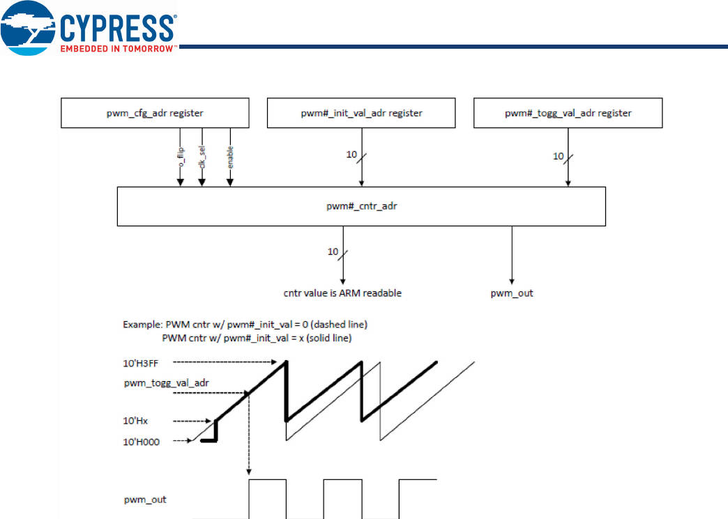
PWM
The CYBT-X430XX-01 has four PWMs. The PWM module consists of the following:
nPWM0-3
nThe following GPIOs can be mapped as PWMs, module pad shown in [ ]:
pP26 on P12/P26 [Pad 5]
pP27 on P11/P27 [Pad 4]
pP14 on P14/P38 [Pad 7]
pP13 on P13/P28 [Pad 8]
nPWM1-4: Each of the four PWM channels contains the following registers:
p10-bit initial value register (read/write)
p10-bit toggle register (read/write)
p10-bit PWM counter value register (read)
nPWM configuration register shared among PWM1-4 (read/write). This 12-bit register is used:
pTo configure each PWM channel
pTo select the clock of each PWM channel
pTo change the phase of each PWM channel
Figure 11 shows the structure of one PWM.
Document Number: 002-19525 Rev. ** Page 23 of 49
PRELIMINARY
CYBT-343026-01
CYBT-343029-01
CYBT-143038-01
Figure 11. PWM Block Diagram
Triac Control/PWM
The CYBT-X430XX-01 includes hardware support for zero-crossing detection and trigger control for up to two triacs (PAD 22/23). The
CYBT-X430XX-01 detects zero-crossing on the AC zero detection line and uses that to provide a pulse that is offset from the zero
crossing. This allows the CYBT-X430XX-01 to be used in dimmer applications, as well as any other applications that require a control
signal that is offset from an input event.
The zero-crossing hardware includes an option to suppress glitches.
Serial Peripheral Interface
The CYBT-X430XX-01 has two independent SPI interfaces. One is a master-only interface (SPI2) and the other (SPI1) can be either
a master or a slave. Each interface has a 64-byte transmit buffer and a 64-byte receive buffer. To support more flexibility for user
applications, the CYBT-X430XX-01 has optional I/O ports that can be configured individually and separately for each functional pin.
The CYBT-X430XX-01 acts as an SPI master device that supports 1.8V or 3.3V SPI slaves. The CYBT-X430XX-01 can also act as
an SPI slave device that supports a 1.8V or 3.3V SPI master.
SPI voltage depends on VDD; therefore, it defines the type of devices that can be supported.
Power Management Unit
The Power Management Unit (PMU) provides power management features that can be invoked by software through power
management registers or packet-handling in the baseband core.
RF Power Management
The BBC generates power-down control signals for the transmit path, receive path, PLL, and power amplifier to the 2.4 GHz trans-
ceiver, which then processes the power-down functions accordingly.

Document Number: 002-19525 Rev. ** Page 24 of 49
PRELIMINARY
CYBT-343026-01
CYBT-343029-01
CYBT-143038-01
Host Controller Power Management
Power is automatically managed by the firmware based on input device activity. As a power-saving task, the firmware controls the
disabling of the on-chip regulator when in deep sleep (HIDOFF) mode.
BBC Power Management
There are several low-power operations for the BBC:
nPhysical layer packet handling turns RF on and off dynamically within packet TX and RX.
nBluetooth-specified low-power connection mode. While in these low-power connection modes, the CYBT-X430XX-01 runs on the
Low Power Oscillator and wakes up after a predefined time period.
The CYBT-X430XX-01 automatically adjusts its power dissipation based on user activity. The following power modes are supported:
nActive mode
nIdle mode
nSleep mode
nHIDOFF (Deep Sleep) mode
The CYBT-X430XX-01 transitions to the next lower state after a programmable period of user inactivity. Busy mode is immediately
entered when user activity resumes.
In HIDOFF (Deep Sleep) mode, the CYBT-X430XX-01 baseband and core are powered off by disabling power to LDOOUT. The VDDO
domain remains powered up and will turn the remainder of the chip on when it detects user events. This mode minimizes chip power
consumption and is intended for long periods of inactivity.
Document Number: 002-19525 Rev. ** Page 25 of 49
PRELIMINARY
CYBT-343026-01
CYBT-343029-01
CYBT-143038-01
Electrical Characteristics
Tab le 11 shows the maximum electrical rating for voltages referenced to VDD pin.
Tab le 12 shows the power supply characteristics for the range TJ = 0 to 125 °C.
Tab le 13 shows the specifications for the digital voltage levels.
Tab le 9 shows the current consumption measurements
Table 11. Maximum Electrical Rating
Rating Symbol Value Unit
VDDIN – 3.795 V
Voltage on input or output pin – VSS – 0.3 to VDD + 0.3 V
Operating ambient temperature range Topr –30 to +85 °C
Storage temperature range Tstg –40 to +125 °C
Table 12. Power Supply
Parameter Description Minimum1
1. Overall performance degrades beyond minimum and maximum supply voltages.
Typical Maximum1Unit
VDDIN Power Supply Input for CYBT-34302X-01 2.30 – 3.6 V
VDDIN Power Supply Input for CYBT-143038-01 1.62 – 3.6 V
Table 13. Digital Levels
Characteristics Symbol Min Typ Max Unit
Input low voltage VIL ––0.8V
Input high voltage VIH 2.0 – – V
Output low voltage VOL ––0.4V
Output high voltage VOH VDD – 0.4 – – V
Input capacitance (VDDMEM domain) CIN ––0.4pF
Table 14. Bluetooth, BLE, BR and EDR Current Consumption, Class 1
Mode Remarks Typ. Unit
3DH5/3DH5 –37.10mA
BLE
nBLE Connected 600 ms interval 211 A
nBLE ADV Unconnectable 1.00 sec 176 ?A
nBLE Scan No devices present. A 1.28 second interval with a scan window of 11.25 ms 355 ?A
DMx/DHx
nDM1/DH1 – 32.15 mA
nDM3/DH3 – 38.14 mA
nDM5/DH5 – 38.46 mA
HIDOFF Deep sleep 2.69 ?A
Page scan Periodic scan rate is 1.28 sec 0.486 mA
Receive
n1 Mbps Peak current level during reception of a basic-rate packet. 26.373 mA
nEDR Peak current level during the reception of a 2 or 3 Mbps rate packet. 26.373 mA

Document Number: 002-19525 Rev. ** Page 26 of 49
PRELIMINARY
CYBT-343026-01
CYBT-343029-01
CYBT-143038-01
Sniff Slave
n11.25 ms – 4.95 mA
n22.5 ms – 2.6 mA
n495.00 ms Based on one attempt and no timeout. 254 ?A
Transmit
n1 Mbps Peak current level during the transmission of a basic-rate packet: GFSK
output power = 10 dBm. 60.289 mA
nEDR Peak current level during the transmission of a 2 or 3 Mbps rate packet. EDR
output power = 8 dBm. 52.485 mA
Table 15. Bluetooth and BLE Current Consumption, Class 2 (0 dBm)
Mode Remarks Typ. Unit
3DH5/3DH5 – 31.57 mA
BLE
nBLE ADV Unconnectable 1.00 sec 174 ?A
nBLE Scan No devices present. A 1.28 second interval with a scan window of 11.25 ms 368 ?A
DMx/DHx
nDM1/DH1 – 27.5 mA
nDM3/DH3 – 31.34 mA
nDM5/DH5 – 32.36 mA
Table 14. Bluetooth, BLE, BR and EDR Current Consumption, Class 1

Document Number: 002-19525 Rev. ** Page 27 of 49
PRELIMINARY
CYBT-343026-01
CYBT-343029-01
CYBT-143038-01
RF Specifications
All specifications in Tab le 16 are for industrial temperatures and are single-ended. Unused inputs are left open.
Table 16. Receiver RF Specifications
Parameter Conditions Minimum Typical 1Maximum Unit
General
Frequency range – 2402 – 2480 MHz
RX sensitivity 2
GFSK, 0.1% BER, 1 Mbps – –93.5 – dBm
LE GFSK, 0.1% BER, 1 Mbps – –96.5 – dBm
π/4-DQPSK, 0.01% BER, 2 Mbps – –95.5 – dBm
8-DPSK, 0.01% BER, 3 Mbps – –89.5 – dBm
Maximum input GFSK, 1 Mbps – – –20 dBm
Maximum input π/4-DQPSK, 8-DPSK, 2/3 Mbps – – –20 dBm
Interference Performance
C/I cochannel GFSK, 0.1% BER – 9.5 11 dB
C/I 1 MHz adjacent channel GFSK, 0.1% BER – –5 0 dB
C/I 2 MHz adjacent channel GFSK, 0.1% BER – –40 –30.0 dB
C/I > 3 MHz adjacent channel GFSK, 0.1% BER – –49 –40.0 dB
C/I image channel GFSK, 0.1% BER – –27 –9.0 dB
C/I 1 MHz adjacent to image
channel GFSK, 0.1% BER – –37 –20.0 dB
C/I cochannel π/4-DQPSK, 0.1% BER – 11 13 dB
C/I 1 MHz adjacent channel π/4-DQPSK, 0.1% BER – –8 0 dB
C/I 2 MHz adjacent channel π/4-DQPSK, 0.1% BER – –40 –30.0 dB
C/I > 3 MHz adjacent channel 8-DPSK, 0.1% BER – –50 –40.0 dB
C/I image channel π/4-DQPSK, 0.1% BER – –27 –7.0 dB
C/I 1 MHz adjacent to image
channel π/4-DQPSK, 0.1% BER – –40 –20.0 dB
C/I cochannel 8-DPSK, 0.1% BER – 17 21 dB
C/I 1 MHz adjacent channel 8-DPSK, 0.1% BER – –5 5 dB
C/I 2 MHz adjacent channel 8-DPSK, 0.1% BER – –40 –25.0 dB
C/I > 3 MHz adjacent channel 8-DPSK, 0.1% BER – –47 –33.0 dB
C/I Image channel 8-DPSK, 0.1% BER – –20 0 dB
C/I 1 MHz adjacent to image
channel 8-DPSK, 0.1% BER – –35 –13.0 dB
Out-of-Band Blocking Performance (CW)3
30 MHz–2000 MHz 0.1% BER – –10.0 – dBm
2000–2399 MHz 0.1% BER – –27 – dBm
2498–3000 MHz 0.1% BER – –27 – dBm
3000 MHz–12.75 GHz 0.1% BER – –10.0 – dBm
Document Number: 002-19525 Rev. ** Page 28 of 49
PRELIMINARY
CYBT-343026-01
CYBT-343029-01
CYBT-143038-01
Out-of-Band Blocking Performance, Modulated Interferer
776–764 MHz CDMA – –104–dBm
824–849 MHz CDMA – –10<Super-
script>4 –dBm
1850–1910 MHz CDMA – –23<Super-
script>4 –dBm
824–849 MHz EDGE/GSM – –10<Super-
script>4 –dBm
880–915 MHz EDGE/GSM – –10<Super-
script>4 –dBm
1710–1785 MHz EDGE/GSM – –23<Super-
script>4 –dBm
1850–1910 MHz EDGE/GSM – –23<Super-
script>4 –dBm
1850–1910 MHz WCDMA – –23<Super-
script>4 –dBm
1920–1980 MHz WCDMA – –23<Super-
script>4 –dBm
Intermodulation Performance5
BT, Df = 5 MHz – –39.0 – – dBm
Spurious Emissions6
30 MHz to 1 GHz – – – –62 dBm
1 GHz to 12.75 GHz – – – –47 dBm
65 MHz to 108 MHz FM Rx – –147 – dBm/Hz
746 MHz to 764 MHz CDMA – –147 – dBm/Hz
851–894 MHz CDMA – –147 – dBm/Hz
925–960 MHz EDGE/GSM – –147 – dBm/Hz
1805–1880 MHz EDGE/GSM – –147 – dBm/Hz
1930–1990 MHz PCS – –147 – dBm/Hz
2110–2170 MHz WCDMA – –147 – dBm/Hz
1. Typical operating conditions are 1.22V operating voltage and 25°C ambient temperature.
2. The receiver sensitivity is measured at BER of 0.1% on the device interface.
3. Meets this specification using front-end band pass filter.
4. Numbers are referred to the pin output with an external BPF filter.
5. f0 = -64 dBm Bluetooth-modulated signal, f1 = –39 dBm sine wave, f2 = –39 dBm Bluetooth-modulated signal, f0 = 2f1 – f2, and |f2 – f1| = n*1 MHz, where n is 3, 4, or
5. For the typical case, n = 4.
6. Includes baseband radiated emissions.
Table 16. Receiver RF Specifications (continued)
Parameter Conditions Minimum Typical 1Maximum Unit
Document Number: 002-19525 Rev. ** Page 29 of 49
PRELIMINARY
CYBT-343026-01
CYBT-343029-01
CYBT-143038-01
Table 17. Transmitter RF Specifications
Table 18. BLE RF Specifications
Parameter Conditions Minimum Typical Maximum Unit
General
Frequency range – 2402 – 2480 MHz
Class1: GFSK Tx power1
1. TBD dBm output for GFSK measured with PAVDD = 2.5V.
––12–dBm
Class1: EDR Tx power2
2. TBD dBm output for EDR measured with PAVDD = 2.5V.
––9–dBm
Class 2: GFSK Tx power – – 2 – dBm
Power control step – 2 4 8 dB
Modulation Accuracy
π/4-DQPSK Frequency Stability – –10 – 10 kHz
π/4-DQPSK RMS DEVM – – – 20 %
π/4-QPSK Peak DEVM – – – 35 %
π/4-DQPSK 99% DEVM – – – 30 %
8-DPSK frequency stability – –10 – 10 kHz
8-DPSK RMS DEVM – – – 13 %
8-DPSK Peak DEVM – – – 25 %
8-DPSK 99% DEVM – – – 20 %
In-Band Spurious Emissions
1.0 MHz < |M – N| < 1.5 MHz – – – –26 dBc
1.5 MHz < |M – N| < 2.5 MHz – – – –20 dBm
|M – N| > 2.5 MHz – – – –40 dBm
Out-of-Band Spurious Emissions
30 MHz to 1 GHz – – – –36.03
3. Maximum value is the value required for Bluetooth qualification.
dBm
1 GHz to 12.75 GHz – – – –30.0<Super-
script>3, 4
4. Meets this spec using a front-end band-pass filter.
dBm
1.8 GHz to 1.9 GHz – – – –47.0 dBm
5.15 GHz to 5.3 GHz – – – –47.0 dBm
Parameter Conditions Minimum Typical Maximum Unit
Frequency range N/A 2402 – 2480 MHz
Rx sense1
1. Dirty Tx is Off.
GFSK, 0.1% BER, 1 Mbps – –96.5 – dBm
Tx power2
2. The BLE Tx power can be increased to compensate for front-end losses such as BPF, diplexer, switch, etc. The output is capped at 12 dBm out. The BLE Tx power
at the antenna port cannot exceed the 10 dBm EIRP specification limit.
N/A –9–dBm
Mod Char: Delta F1 average N/A 225 255 275 kHz
Mod Char: Delta F2 max3
3. At least 99.9% of all delta F2 max frequency values recorded over 10 packets must be greater than 185 kHz.
N/A 99.9 – – %
Mod Char: Ratio N/A 0.8 0.95 – %
Document Number: 002-19525 Rev. ** Page 30 of 49
PRELIMINARY
CYBT-343026-01
CYBT-343029-01
CYBT-143038-01
Timing and AC Characteristics
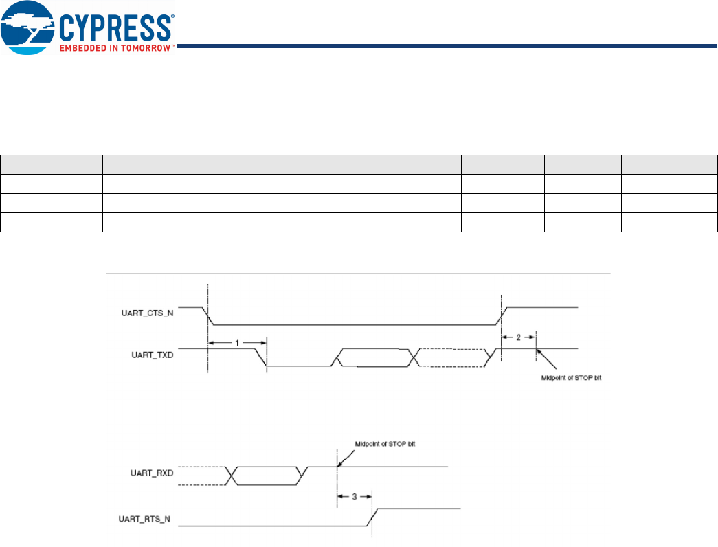
In this section, use the numbers listed in the Reference column of each table to interpret the following timing diagrams.
UART Timing
Figure 12. UART Timing
Table 19. UART Timing Specifications
Reference Characteristics Min Max Unit
1 Delay time, UART_CTS_N low to UART_TXD valid – 24 Baud out cycles
2 Setup time, UART_CTS_N high before midpoint of stop bit – 10 ns
3 Delay time, midpoint of stop bit to UART_RTS_N high – 2 Baud out cycles
Document Number: 002-19525 Rev. ** Page 31 of 49
PRELIMINARY
CYBT-343026-01
CYBT-343029-01
CYBT-143038-01
SPI Timing
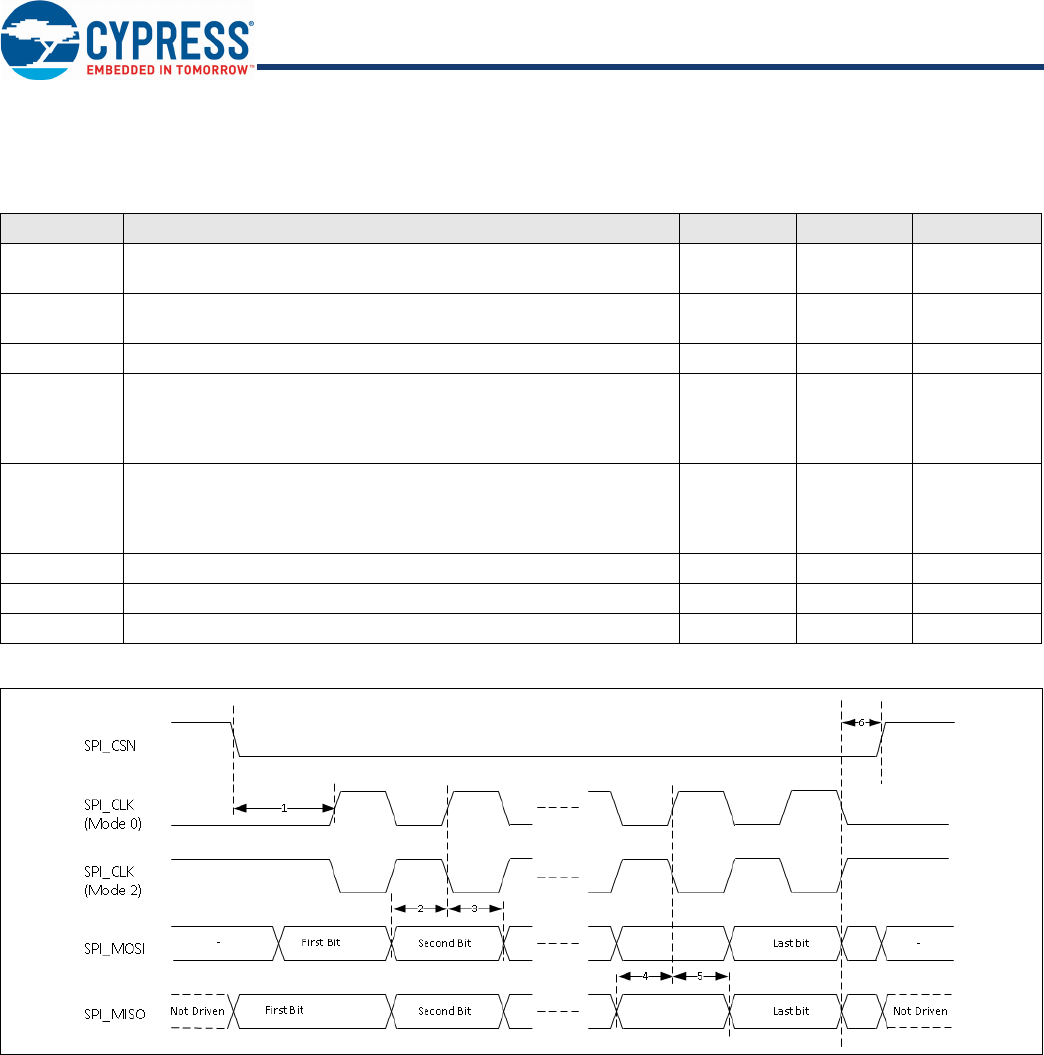
The SPI interface supports clock speeds up to 12 MHz
Tab le 20 and Figure 13 show the timing requirements when operating in SPI Mode 0 and 2, and SPI Mode 1 and 3, respectively.
Table 20. SPI Mode 0 and 2
Figure 13. SPI Timing – Mode 0 and 2
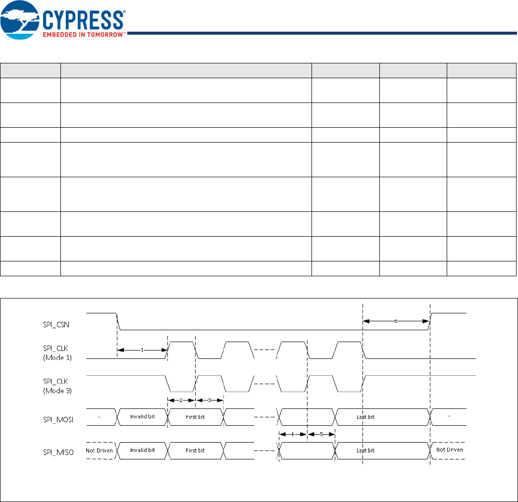
Tab le 21 and Figure 14 show the timing requirements when operating in SPI Mode 1 and 3.
Reference Characteristics Minimum Maximum Unit
1Time from slave assert SPI_INT to master assert SPI_CSN (Direc-
tRead) 0?ns
2Time from master assert SPI_CSN to slave assert SPI_INT (Direct-
Write) 0?ns
3 Time from master assert SPI_CSN to first clock edge 20 ? ns
4 Setup time for MOSI data lines 8
<FmNumerator
>1/<FmDeno
minator>2
SCK
ns
5 Hold time for MOSI data lines 8
<FmNumerator
>1/<FmDeno
minator>2
SCK
ns
6 Time from last sample on MOSI/MISO to slave deassert SPI_INT 0 100 ns
7 Time from slave deassert SPI_INT to master deassert SPI_CSN 0 ? ns
8 Idle time between subsequent SPI transactions 1 SCK ? ns
Document Number: 002-19525 Rev. ** Page 32 of 49
PRELIMINARY
CYBT-343026-01
CYBT-343029-01
CYBT-143038-01
Table 21. SPI Mode 1 and 3
Figure 14. SPI Timing – Mode 1 and 3
Reference Characteristics Minimum Maximum Unit
1Time from slave assert SPI_INT to master assert
SPI_CSN (DirectRead) 0?ns
2Time from master assert SPI_CSN to slave assert
SPI_INT (DirectWrite) 0?ns
3 Time from master assert SPI_CSN to first clock edge 20 ? ns
4 Setup time for MOSI data lines 8
<FmNumerator>1
/<FmDenomi-
nator>2 SCK
ns
5 Hold time for MOSI data lines 8
<FmNumerator>1
/<FmDenomi-
nator>2 SCK
ns
6Time from last sample on MOSI/MISO to slave
deassert SPI_INT 0 100 ns
7Time from slave deassert SPI_INT to master
deassert SPI_CSN 0?ns
8 Idle time between subsequent SPI transactions 1 SCK ? ns
Document Number: 002-19525 Rev. ** Page 33 of 49
PRELIMINARY
CYBT-343026-01
CYBT-343029-01
CYBT-143038-01
BSC Interface Timing
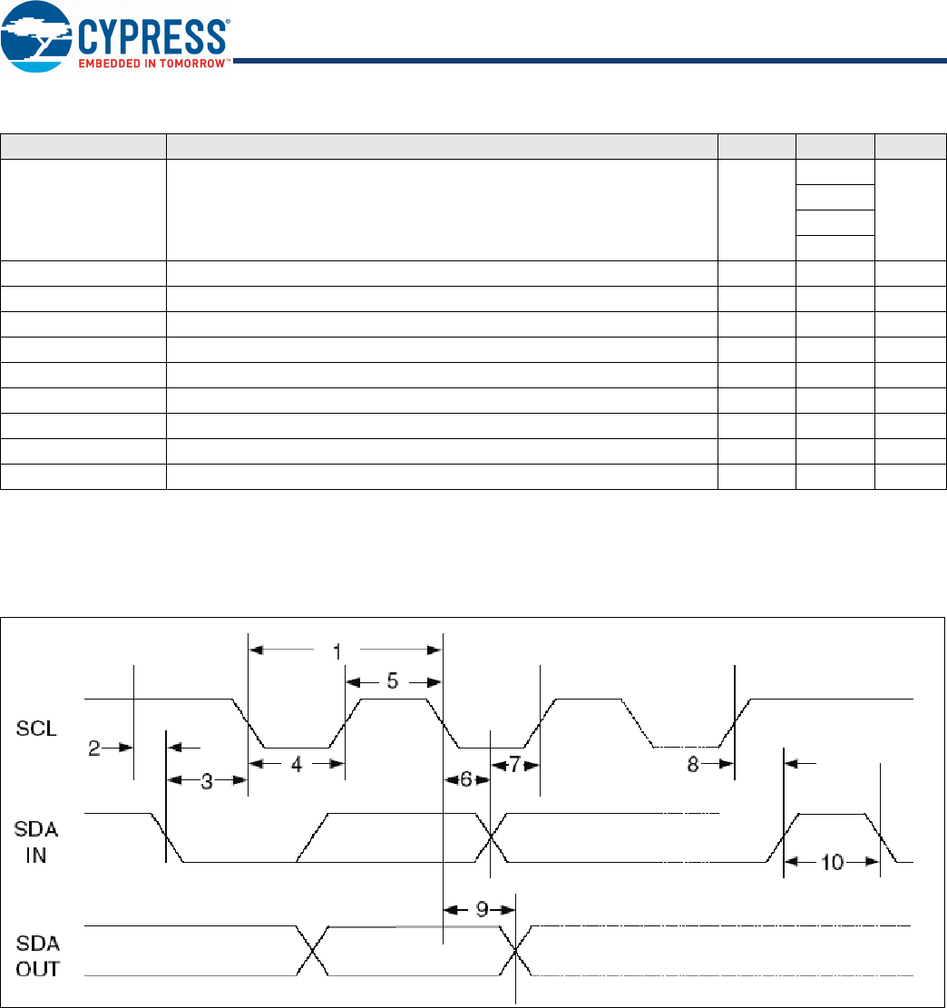
Figure 15. BSC Interface Timing Diagram
Table 22. BSC Interface Timing Specifications
Reference Characteristics Min Max Unit
1 Clock frequency – 100 kHz
400
800
1000
2 START condition setup time 650 – ns
3 START condition hold time 280 – ns
4 Clock low time 650 – ns
5 Clock high time 280 – ns
6 Data input hold time1
1. As a transmitter, 125 ns of delay is provided to bridge the undefined region of the falling edge of SCL to avoid unintended generation of START
or STOP conditions.
0 – ns
7 Data input setup time 100 – ns
8 STOP condition setup time 280 – ns
9 Output valid from clock – 400 ns
10 Bus free time2
2. Time that the cbus must be free before a new transaction can start.
650 – ns
Document Number: 002-19525 Rev. ** Page 34 of 49
PRELIMINARY
CYBT-343026-01
CYBT-343029-01
CYBT-143038-01
PCM Interface Timing
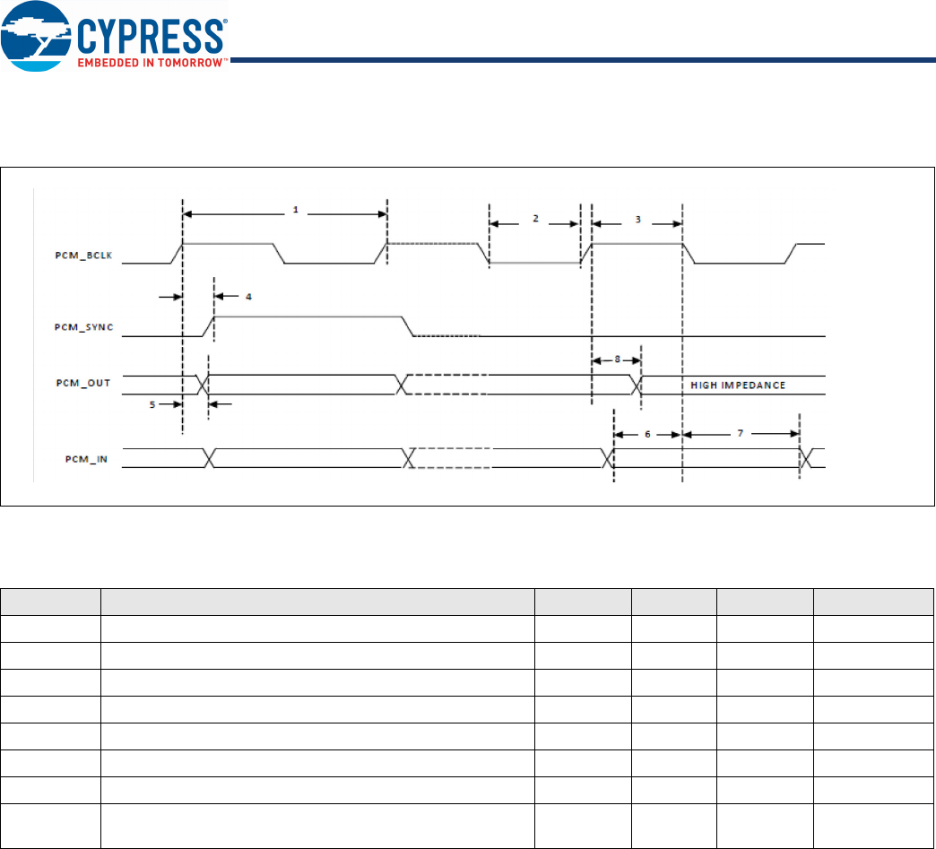
Short Frame Sync, Master Mode
Figure 16. PCM Timing Diagram (Short Frame Sync, Master Mode)
Table 23. PCM Interface Timing Specifications (Short Frame Sync, Master Mode)
Reference Characteristics Minimum Typical Maximum Unit
1 PCM bit clock frequency – – 20.0 MHz
2 PCM bit clock LOW 20.0 – – ns
3 PCM bit clock HIGH 20.0 – – ns
4 PCM_SYNC delay 0 – 5.7 ns
5 PCM_OUT delay –0.4 – 5.6 ns
6 PCM_IN setup 16.9 – – ns
7 PCM_IN hold 25.0 – – ns
8Delay from rising edge of PCM_BCLK during last bit period
to PCM_OUT becoming high impedance –0.4 – 5.6 ns
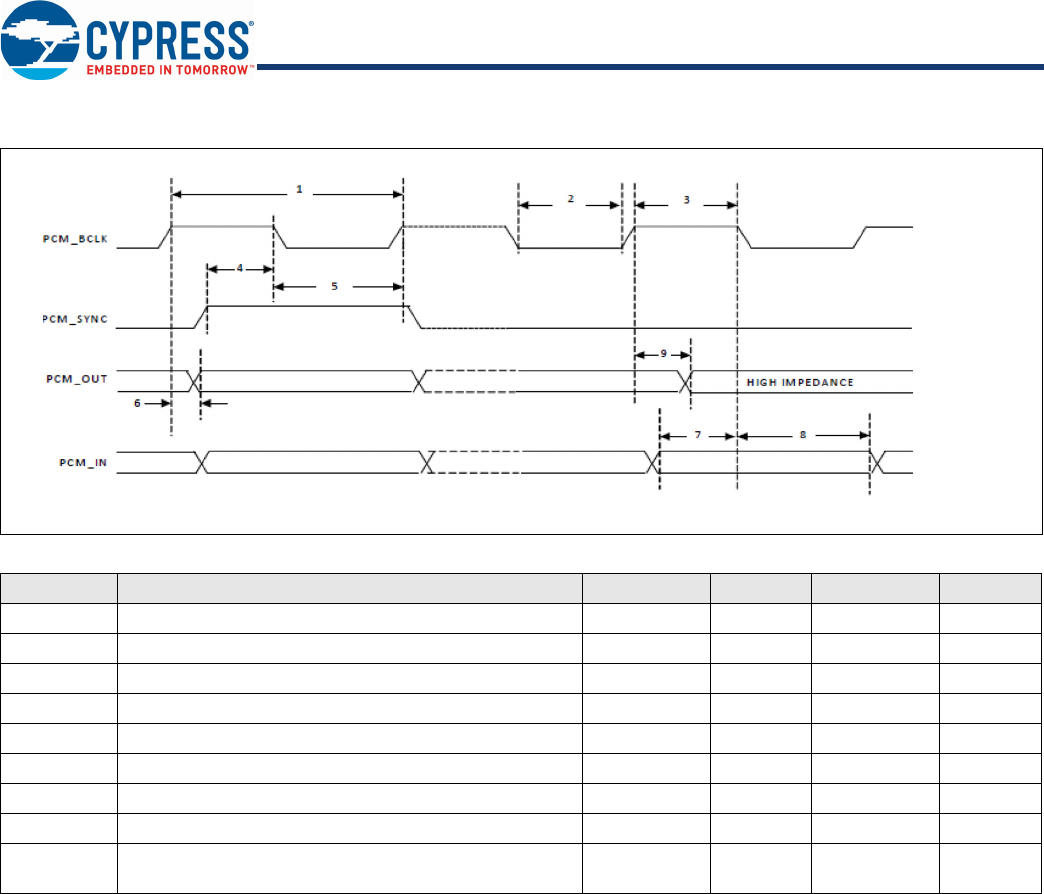
Document Number: 002-19525 Rev. ** Page 35 of 49
PRELIMINARY
CYBT-343026-01
CYBT-343029-01
CYBT-143038-01
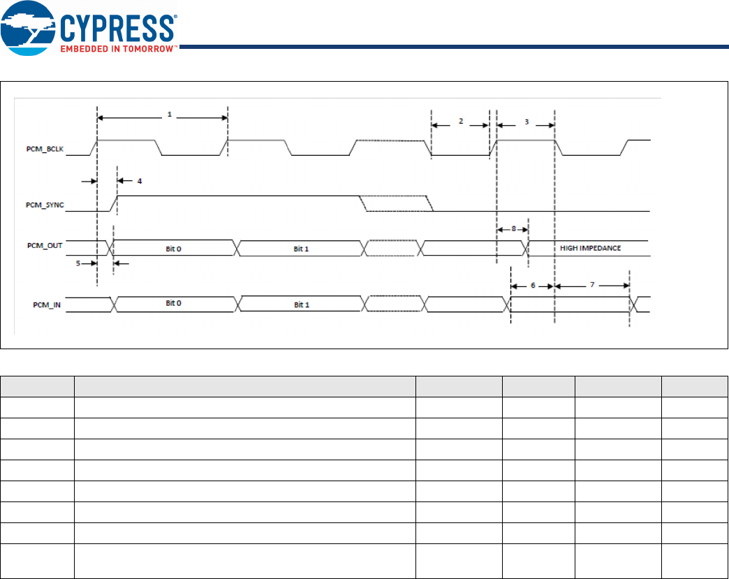
Short Frame Sync, Slave Mode
Figure 17. PCM Timing Diagram (Short Frame Sync, Slave Mode)
Table 24. PCM Interface Timing Specifications (Short Frame Sync, Slave Mode)
Reference Characteristics Minimum Typical Maximum Unit
1 PCM bit clock frequency – – TBD MHz
2 PCM bit clock LOW TBD – – ns
3 PCM bit clock HIGH TBD – – ns
4 PCM_SYNC setup TBD – – ns
5 PCM_SYNC hold TBD – – ns
6 PCM_OUT delay TBD – TBD ns
7 PCM_IN setup TBD – – ns
8 PCM_IN hold TBD – – ns
9Delay from rising edge of PCM_BCLK during last bit period
to PCM_OUT becoming high impedance TBD – TBD ns
Document Number: 002-19525 Rev. ** Page 36 of 49
PRELIMINARY
CYBT-343026-01
CYBT-343029-01
CYBT-143038-01
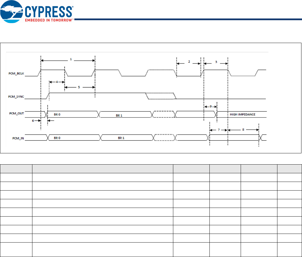
Figure 18. PCM Timing Diagram (Long Frame Sync, Master Mode)
Table 25. PCM Interface Timing Specifications (Long Frame Sync, Master Mode)
Reference Characteristics Minimum Typical Maximum Unit
1 PCM bit clock frequency – – TBD MHz
2 PCM bit clock LOW TBD – – ns
3 PCM bit clock HIGH TBD – – ns
4 PCM_SYNC delay TBD – TBD ns
5 PCM_OUT delay TBD – TBD ns
6 PCM_IN setup TBD – – ns
7 PCM_IN hold TBD – – ns
8Delay from rising edge of PCM_BCLK during last bit period
to PCM_OUT becoming high impedance TBD – TBD ns
Document Number: 002-19525 Rev. ** Page 37 of 49
PRELIMINARY
CYBT-343026-01
CYBT-343029-01
CYBT-143038-01
Long Frame Sync, Slave Mode
Figure 19. PCM Timing Diagram (Long Frame Sync, Slave Mode)
Table 26. PCM Interface Timing Specifications (Long Frame Sync, Slave Mode)
Reference Characteristics Minimum Typical Maximum Unit
1 PCM bit clock frequency – – TBD MHz
2 PCM bit clock LOW TBD – – ns
3 PCM bit clock HIGH TBD – – ns
4 PCM_SYNC setup TBD – – ns
5 PCM_SYNC hold TBD – – ns
6 PCM_OUT delay TBD – TBD ns
7 PCM_IN setup TBD – – ns
8 PCM_IN hold TBD – – ns
9Delay from rising edge of PCM_BCLK during last bit period
to PCM_OUT becoming high impedance TBD – TBD ns
Document Number: 002-19525 Rev. ** Page 38 of 49
PRELIMINARY
CYBT-343026-01
CYBT-343029-01
CYBT-143038-01
I2S Interface Timing
The I2S interface supports both master and slave modes. The I2S signals are:
nI2S clock: I2S SCK
nI2S Word Select: I2S WS
nI2S Data Out: I2S SDO
nI2S Data In: I2S SDI
I2S SCK and I2S WS become outputs in master mode and inputs in slave mode, while I2S SDO always stays as an output. The channel
word length is 16 bits and the data is justified so that the MSB of the left-channel data is aligned with the MSB of the I2S bus, per the
I2S specification. The MSB of each data word is transmitted one bit clock cycle after the I2S WS transition, synchronous with the falling
edge of bit clock. Left-channel data is transmitted when I2S WS is low, and right-channel data is transmitted when I2S WS is high.
Data bits sent by the CYBT-013033-01 are synchronized with the falling edge of I2S_SCK and should be sampled by the receiver on
the rising edge of I2S_SSCK.
The clock rate in master mode is either of the following:
n48 kHz x 32 bits per frame = 1.536 MHz
n48 kHz x 50 bits per frame = 2.400 MHz
The master clock is generated from the input reference clock using a N/M clock divider. In the slave mode, any clock rate is supported
to a maximum of 3.072 MHz. Timing values specified in Ta b le 27 are relative to high and low threshold levels.
Table 27. Timing for I2S Transmitters and Receivers
Transmitter Receiver
Notes
Lower LImit Upper Limit Lower Limit Upper Limit
Min Max Min Max Min Max Min Max
Clock Period T Ttr –––
Tr––– 1
1. The system clock period T must be greater than Ttr and Tr because both the transmitter and receiver have to be able to handle the data transfer rate.
Master Mode: Clock generated by transmitter or receiver
HIGH tHC 0.35Ttr –––
0.35Ttr –––2
2. At all data rates in master mode, the transmitter or receiver generates a clock signal with a fixed mark/space ratio. For this reason, tHC and tLC are specified with
respect to T.
LOWtLC 0.35Ttr –––
0.35Ttr –––2
Slave Mode: Clock accepted by transmitter or receiver
HIGH tHC –0.35Ttr –––
0.35Ttr –– 3
3. In slave mode, the transmitter and receiver need a clock signal with minimum HIGH and LOW periods so that they can detect the signal. So long as the minimum
periods are greater than 0.35Tr, any clock that meets the requirements can be used.
LOW tLC –0.35Ttr –––
0.35Ttr –– 3
Rise time tRC ––
0.15Ttr ––– –4
4. Because the delay (tdtr) and the maximum transmitter speed (defined by Ttr) are related, a fast transmitter driven by a slow clock edge can result in tdtr not
exceeding tRC which means thtr becomes zero or negative. Therefore, the transmitter has to guarantee that thtr is greater than or equal to zero, so long as the
clock rise-time tRC is not more than tRCmax, where tRCmax is not less than 0.15Ttr.
Transmitter
Delay tdtr –––0.8T––––5
5. To allow data to be clocked out on a falling edge, the delay is specified with respect to the rising edge of the clock signal and T, always giving the receiver sufficient
setup time.
Hold time thtr 0––––––– 5
Receiver
Setup time tsr –––––
0.2Tr––6
6. The data setup and hold time must not be less than the specified receiver setup and hold time.
Hold time thr –––––0––6
Document Number: 002-19525 Rev. ** Page 39 of 49
PRELIMINARY
CYBT-343026-01
CYBT-343029-01
CYBT-143038-01
Environmental Specifications
Environmental Compliance
This CYBT-X430XX-01 BLE module is produced in compliance with the Restriction of Hazardous Substances (RoHS) and
Halogen-Free (HF) directives. The Cypress module and components used to produce this module are RoHS and HF compliant.
RF Certification
The CYBT-X430XX-01 module will be certified under the following RF certification standards at production release.
nFCC: WAP3026
nCE
nIC: 7922A-3026
nMIC: TBD
Safety Certification
The CYBT-X430XX-01 module complies with the following safety regulations:
nUnderwriters Laboratories, Inc. (UL): Filing E331901
nCSA
nTUV
Environmental Conditions
Tab le 28 describes the operating and storage conditions for the Cypress BLE module.
ESD and EMI Protection
Exposed components require special attention to ESD and electromagnetic interference (EMI).
A grounded conductive layer inside the device enclosure is suggested for EMI and ESD performance. Any openings in the enclosure
near the module should be surrounded by a grounded conductive layer to provide ESD protection and a low-impedance path to ground.
Device Handling: Proper ESD protocol must be followed in manufacturing to ensure component reliability.
Table 28. Environmental Conditions for CYBT-X430XX-01
Description Minimum Specification Maximum Specification
Operating temperature −30 °C 85 °C
Operating humidity (relative, non-condensation) 5% 85%
Thermal ramp rate – 3 °C/minute
Storage temperature –40 °C 85 °C
Storage temperature and humidity – 85 °C at 85%
ESD: Module integrated into system Components[4] –15 kV Air
2.0 kV Contact
Note
4. This does not apply to the RF pins (ANT).

Document Number: 002-19525 Rev. ** Page 40 of 49
PRELIMINARY
CYBT-343026-01
CYBT-343029-01
CYBT-143038-01
Regulatory Information
FCC
FCC NOTICE:
The device CYBT-X430XX-01 complies with Part 15 of the FCC Rules. The device meets the requirements for modular transmitter
approval as detailed in FCC public Notice DA00-1407.transmitter Operation is subject to the following two conditions: (1) This device
may not cause harmful interference, and (2) This device must accept any interference received, including interference that may cause
undesired operation.
CAUTION:
The FCC requires the user to be notified that any changes or modifications made to this device that are not expressly approved by
Cypress Semiconductor may void the user's authority to operate the equipment.
This equipment has been tested and found to comply with the limits for a Class B digital device, pursuant to Part 15 of the FCC Rules.
These limits are designed to provide reasonable protection against harmful interference in a residential installation. This equipment
generates uses and can radiate radio frequency energy and, if not installed and used in accordance with the instructions,ê may cause
harmful interference to radio communications. However, there is no guarantee that interference will not occur in a particular installation.
If this equipment does cause harmful interference to radio or television reception, which can be determined by turning the equipment
off and on, the user is encouraged to try to correct the interference by one or more of the following measures:
nReorient or relocate the receiving antenna.
nIncrease the separation between the equipment and receiver.
nConnect the equipment into an outlet on a circuit different from that to which the receiver is connected.
nConsult the dealer or an experienced radio/TV technician for help
LABELING REQUIREMENTS:
The Original Equipment Manufacturer (OEM) must ensure that FCC labelling requirements are met. This includes a clearly visible
label on the outside of the OEM enclosure specifying the appropriate Cypress Semiconductor FCC identifier for this product as well
as the FCC Notice above. The FCC identifier is FCC ID: WAP3026.
In any case the end product must be labeled exterior with "Contains FCC ID: WAP3026"
ANTENNA WARNING:
This device is tested with a standard SMA connector and with the antenna listed in Table 7 on page 13. When integrated in the OEMs
product, these fixed antennas require installation preventing end-users from replacing them with non-approved antennas. Any antenna
not in the following table must be tested to comply with FCC Section 15.203 for unique antenna connectors and Section 15.247 for
emissions.
RF EXPOSURE:
To comply with FCC RF Exposure requirements, the Original Equipment Manufacturer (OEM) must ensure to install the approved
antenna in the previous.
The preceding statement must be included as a CAUTION statement in manuals, for products operating with the approved antenna
in Table 7 on page 13, to alert users on FCC RF Exposure compliance. Any notification to the end user of installation or removal
instructions about the integrated radio module is not allowed.
The radiated output power of CYBT-X430XX-01 with the trace antenna is far below the FCC radio frequency exposure limits. Never-
theless, use CYBT-X430XX-01 in such a manner that minimizes the potential for human contact during normal operation.
End users may not be provided with the module installation instructions. OEM integrators and end users must be provided with
transmitter operating conditions for satisfying RF exposure compliance.

Document Number: 002-19525 Rev. ** Page 41 of 49
PRELIMINARY
CYBT-343026-01
CYBT-343029-01
CYBT-143038-01
ISED
Innovation, Science and Economic Development Canada (ISED) Certification
CYBT-X430XX-01 is licensed to meet the regulatory requirements of Innovation, Science and Economic Development Canada (ISED),
License: ISED: 7922A-3026
Manufacturers of mobile, fixed or portable devices incorporating this module are advised to clarify any regulatory questions and ensure
compliance for SAR and/or RF exposure limits. Users can obtain Canadian information on RF exposure and compliance from
www.ic.gc.ca.
This device has been designed to operate with the antennas listed in Table 7 on page 13, having a maximum gain of -0.5 dBi. Antennas
not included in this list or having a gain greater than -0.5 dBi are strictly prohibited for use with this device. The required antenna
impedance is 50 ohms. The antenna used for this transmitter must not be co-located or operating in conjunction with any other antenna
or transmitter.
ISED NOTICE:
The device CYBT-X430XX-01 including the built-in trace antenna complies with Canada RSS-GEN Rules. The device meets the
requirements for modular transmitter approval as detailed in RSS-GEN. Operation is subject to the following two conditions: (1) This
device may not cause harmful interference, and (2) This device must accept any interference received, including interference that
may cause undesired operation.
L'appareil CYBT-X430XX-01, y compris l'antenne intégrée, est conforme aux Règles RSS-GEN de Canada. L'appareil répond aux
exigences d'approbation de l'émetteur modulaire tel que décrit dans RSS-GEN. L'opération est soumise aux deux conditions
suivantes: (1) Cet appareil ne doit pas causer d'interférences nuisibles, et (2) Cet appareil doit accepter toute interférence reçue, y
compris les interférences pouvant entraîner un fonctionnement indésirable.
ISED INTERFERENCE STATEMENT FOR CANADA
This device complies with Innovation, Science and Economic Development (ISED) Canada licence-exempt RSS standard(s).
Operation is subject to the following two conditions: (1) this device may not cause interference, and (2) this device must accept any
interference, including interference that may cause undesired operation of the device.
Cet appareil est conforme à la norme sur l'innovation, la science et le développement économique (ISED) norme RSS exempte de
licence. L'exploitation est autorisée aux deux conditions suivantes : (1) l'appareil ne doit pas produire de brouillage, et (2) l'utilisateur
de l'appareil doit accepter tout brouillage radioélectrique subi, même si le brouillage est susceptible d'en compromettre le fonction-
nement.
ISED RADIATION EXPOSURE STATEMENT FOR CANADA
This equipment complies with ISED radiation exposure limits set forth for an uncontrolled environment.
Cet équipement est conforme aux limites d'exposition aux radiations ISED prévues pour un environnement incontrôlé.
LABELING REQUIREMENTS:
The Original Equipment Manufacturer (OEM) must ensure that ISED labelling requirements are met. This includes a clearly visible
label on the outside of the OEM enclosure specifying the appropriate Cypress Semiconductor IC identifier for this product as well as
the ISED Notices above. The IC identifier is 7922A-3026. In any case, the end product must be labeled in its exterior with "Contains
IC: 7922A-3026"
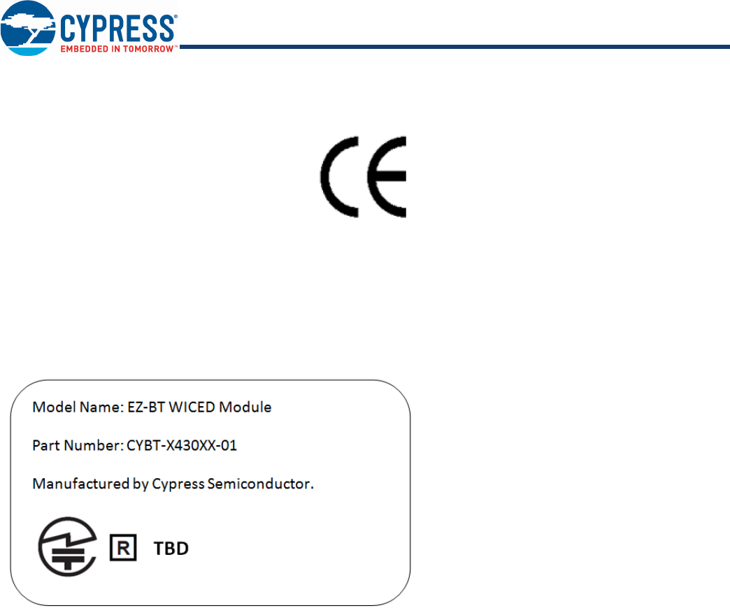
Document Number: 002-19525 Rev. ** Page 42 of 49
PRELIMINARY
CYBT-343026-01
CYBT-343029-01
CYBT-143038-01
European Declaration of Conformity
Hereby, Cypress Semiconductor declares that the Bluetooth module CYBT-X430XX-01 complies with the essential requirements and
other relevant provisions of Directive 2014. As a result of the conformity assessment procedure described in Annex III of the Directive
2014, the end-customer equipment should be labeled as follows:
All versions of the CYBT-X430XX-01 in the specified reference design can be used in the following countries: Austria, Belgium, Cyprus,
Czech Republic, Denmark, Estonia, Finland, France, Germany, Greece, Hungary, Ireland, Italy, Latvia, Lithuania, Luxembourg, Malta,
Poland, Portugal, Slovakia, Slovenia, Spain, Sweden, The Netherlands, the United Kingdom, Switzerland, and Norway.
MIC Japan
CYBT-X430XX-01 is certified as a module with certification number TBD. End products that integrate CYBT-X430XX-01 do not need
additional MIC Japan certification for the end product.
End product can display the certification label of the embedded module.

Document Number: 002-19525 Rev. ** Page 43 of 49
PRELIMINARY
CYBT-343026-01
CYBT-343029-01
CYBT-143038-01
Packaging
The CYBT-X430XX-01 is offered in tape and reel packaging. Figure 20 details the tape dimensions used for the CYBT-X430XX-01.
Figure 20. CYBT-X430XX-01 Tape Dimensions (TBD)
Figure 21 details the orientation of the CYBT-X430XX-01 in the tape as well as the direction for unreeling.
Figure 21. Component Orientation in Tape and Unreeling Direction (TBD)
Table 29. Solder Reflow Peak Temperature
Module Part Number Package Maximum Peak Temperature Maximum Time at Peak Temperature No. of Cycles
CYBT-X430XX-01 24-pad SMT 260 °C 30 seconds 2
Table 30. Package Moisture Sensitivity Level (MSL), IPC/JEDEC J-STD-2
Module Part Number Package MSL
CYBT-X430XX-01 24-pad SMT MSL 3
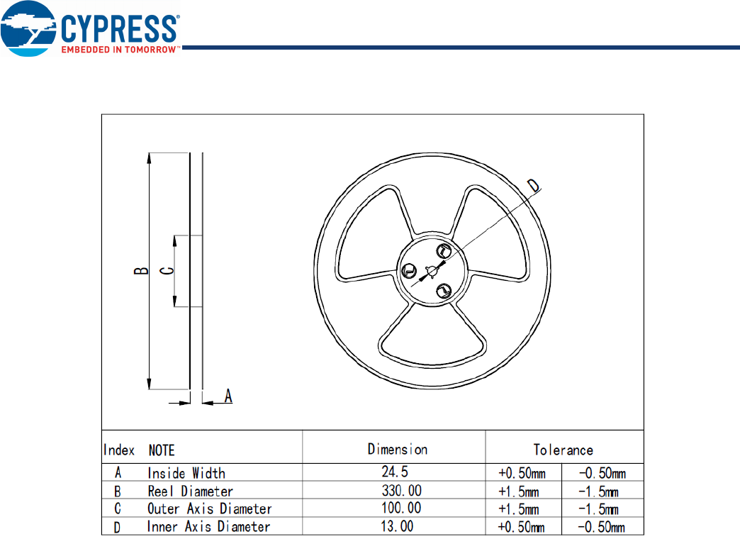
Document Number: 002-19525 Rev. ** Page 44 of 49
PRELIMINARY
CYBT-343026-01
CYBT-343029-01
CYBT-143038-01
Figure 22 details reel dimensions used for the CYBT-X430XX-01.
Figure 22. Reel Dimensions
The CYBT-X430XX-01 is designed to be used with pick-and-place equipment in an SMT manufacturing environment. The
center-of-mass for the CYBT-X430XX-01 is detailed in Figure 23.
Figure 23. CYBT-X430XX-01 Center of Mass (TBD)

Document Number: 002-19525 Rev. ** Page 45 of 49
PRELIMINARY
CYBT-343026-01
CYBT-343029-01
CYBT-143038-01
Ordering Information
Tab le 31 lists the CYBT-X430XX-01 part number and features. Table 32 lists the reel shipment quantities for the CYBT-X430XX-01.
The CYBT-X430XX-01 is offered in tape and reel packaging. The CYBT-X430XX-01 ships in a reel size of TBD.
For additional information and a complete list of Cypress Semiconductor Wireless products, contact your local Cypress sales
representative. To locate the nearest Cypress office, visit our website.
Table 31. Ordering Information
Part Number
CPU
Speed
(MHz)
Flash
Size (KB)
RAM
Size (KB) UART BSC
(I2C)
Apple
Homekit PWM Package Packaging
CYBT-343026-01 24 512 352 Yes Yes No 4 24-SMT Tape and Reel
CYBT-343029-01 24 512 352 Yes Yes Yes 4 24-SMT Tape and Reel
CYBT-143038-01 24 – 352 Yes Yes No 4 24-SMT Tape and Reel
Table 32. Tape and Reel Package Quantity and Minimum Order Amount
Description Minimum Reel Quantity Maximum Reel Quantity Comments
Reel Quantity TBD TBD Ships in TBD unit reel quantities.
Minimum Order Quantity (MOQ) TBD – –
Order Increment (OI) TBD – –
U.S. Cypress Headquarters Address 198 Champion Court, San Jose, CA 95134
U.S. Cypress Headquarter Contact Info (408) 943-2600
Cypress website address http://www.cypress.com
Document Number: 002-19525 Rev. ** Page 46 of 49
PRELIMINARY
CYBT-343026-01
CYBT-343029-01
CYBT-143038-01
Acronyms
Table 33. Acronyms Used in this Document
Acronym Description
BLE Bluetooth Low Energy
Bluetooth SIG Bluetooth Special Interest Group
CE European Conformity
CSA Canadian Standards Association
EMI electromagnetic interference
ESD electrostatic discharge
FCC Federal Communications Commission
GPIO general-purpose input/output
IC Industry Canada
IDE integrated design environment
KC Korea Certification
MIC Ministry of Internal Affairs and Communications
(Japan)
PCB printed circuit board
RX receive
QDID qualification design ID
SMT
surface-mount technology; a method for
producing electronic circuitry in which the
components are placed directly onto the surface
of PCBs
TCPWM timer, counter, pulse width modulator (PWM)
TUV Germany: Technischer Überwachungs-Verein
(Technical Inspection Association)
TX transmit

Document Number: 002-19525 Rev. ** Page 47 of 49
PRELIMINARY
CYBT-343026-01
CYBT-343029-01
CYBT-143038-01
Document Conventions
Units of Measure
Table 34. Units of Measure
Symbol Unit of Measure
°C degree Celsius
kV kilovolt
mA milliamperes
mm millimeters
mV millivolt
μA microamperes
μm micrometers
MHz megahertz
GHz gigahertz
Vvolt

Document Number: 002-19525 Rev. ** Page 48 of 49
PRELIMINARY
CYBT-343026-01
CYBT-343029-01
CYBT-143038-01
Document History Page
Document Title: CYBT-X430XX-01 EZ-BT™ WICED Module
Document Number: 002-19525
Revision ECN Orig. of
Change
Submission
Date Description of Change
** PRELIM-
INARY
DSO Preliminary datasheet for CYBT-X430XX-01 module.

Document Number: 002-19525 Rev. ** Revised May 31, 2017 Page 49 of 49
PRELIMINARY
CYBT-343026-01
CYBT-343029-01
CYBT-143038-01
© Cypress Semiconductor Corporation, 2017. This document is the property of Cypress Semiconductor Corporation and its subsidiaries, including Spansion LLC ("Cypress"). This document, including
any software or firmware included or referenced in this document ("Software"), is owned by Cypress under the intellectual property laws and treaties of the United States and other countries worldwide.
Cypress reserves all rights under such laws and treaties and does not, except as specifically stated in this paragraph, grant any license under its patents, copyrights, trademarks, or other intellectual
property rights. If the Software is not accompanied by a license agreement and you do not otherwise have a written agreement with Cypress governing the use of the Software, then Cypress hereby
grants you a personal, non-exclusive, nontransferable license (without the right to sublicense) (1) under its copyright rights in the Software (a) for Software provided in source code form, to modify and
reproduce the Software solely for use with Cypress hardware products, only internally within your organization, and (b) to distribute the Software in binary code form externally to end users (either
directly or indirectly through resellers and distributors), solely for use on Cypress hardware product units, and (2) under those claims of Cypress's patents that are infringed by the Software (as provided
by Cypress, unmodified) to make, use, distribute, and import the Software solely for use with Cypress hardware products. Any other use, reproduction, modification, translation, or compilation of the
Software is prohibited.
TO THE EXTENT PERMITTED BY APPLICABLE LAW, CYPRESS MAKES NO WARRANTY OF ANY KIND, EXPRESS OR IMPLIED, WITH REGARD TO THIS DOCUMENT OR ANY SOFTWARE
OR ACCOMPANYING HARDWARE, INCLUDING, BUT NOT LIMITED TO, THE IMPLIED WARRANTIES OF MERCHANTABILITY AND FITNESS FOR A PARTICULAR PURPOSE. To the extent
permitted by applicable law, Cypress reserves the right to make changes to this document without further notice. Cypress does not assume any liability arising out of the application or use of any
product or circuit described in this document. Any information provided in this document, including any sample design information or programming code, is provided only for reference purposes. It is
the responsibility of the user of this document to properly design, program, and test the functionality and safety of any application made of this information and any resulting product. Cypress products
are not designed, intended, or authorized for use as critical components in systems designed or intended for the operation of weapons, weapons systems, nuclear installations, life-support devices or
systems, other medical devices or systems (including resuscitation equipment and surgical implants), pollution control or hazardous substances management, or other uses where the failure of the
device or system could cause personal injury, death, or property damage ("Unintended Uses"). A critical component is any component of a device or system whose failure to perform can be reasonably
expected to cause the failure of the device or system, or to affect its safety or effectiveness. Cypress is not liable, in whole or in part, and you shall and hereby do release Cypress from any claim,
damage, or other liability arising from or related to all Unintended Uses of Cypress products. You shall indemnify and hold Cypress harmless from and against all claims, costs, damages, and other
liabilities, including claims for personal injury or death, arising from or related to any Unintended Uses of Cypress products.
Cypress, the Cypress logo, Spansion, the Spansion logo, and combinations thereof, WICED, PSoC, CapSense, EZ-USB, F-RAM, and Traveo are trademarks or registered trademarks of Cypress in
the United States and other countries. For a more complete list of Cypress trademarks, visit cypress.com. Other names and brands may be claimed as property of their respective owners.
Sales, Solutions, and Legal Information
Worldwide Sales and Design Support
Cypress maintains a worldwide network of offices, solution centers, manufacturer’s representatives, and distributors. To find the office
closest to you, visit us at Cypress Locations.
Products
ARM® Cortex® Microcontrollers cypress.com/arm
Automotive cypress.com/automotive
Clocks & Buffers cypress.com/clocks
Interface cypress.com/interface
Internet of Things cypress.com/iot
Memory cypress.com/memory
Microcontrollers cypress.com/mcu
PSoC cypress.com/psoc
Power Management ICs cypress.com/pmic
Touch Sensing cypress.com/touch
USB Controllers cypress.com/usb
Wireless Connectivity cypress.com/wireless
PSoC® Solutions
PSoC 1 | PSoC 3 | PSoC 4 | PSoC 5LP
Cypress Developer Community
Forums | WICED IOT Forums | Projects | Video | Blogs |
Training | Components
Technical Support
cypress.com/support