Cypress Semiconductor 3033 This product is a Bluetooth wireless EZ-BT WICED Module User Manual CYBT 013033 01 EZ BT Module
Cypress Semiconductor This product is a Bluetooth wireless EZ-BT WICED Module CYBT 013033 01 EZ BT Module
User Manual - 0430

PRELIMINARY CYBT-013033-01
EZ-BT™ Module
Cypress Semiconductor Corporation • 198 Champion Court • San Jose,CA 95134-1709 • 408-943-2600
Document Number: 002-18414 Rev. ** Revised January 27, 2017
MNKEZ-BLE™ PRoC™ Module
General Description
The Cypress CYBT-013033-01 is a certified module supporting
dual-mode Bluetooth® Classic (BR/EDR) and Bluetooth® Low
Energy (BLE) wireless communication standards. The
CYBT-013033-01 is a turnkey solution and includes an onboard
crystal oscillator, PCB trace antenna, passive components, and
Cypress CYW20707 silicon device.
The CYBT-013033-01 is a custom RF module design intended
to provide Bluetooth Classic and BLE communication, and allow
up to two GPIO connections for system or module wake events.
The CYBT-013033-01 supports UART and BSC (I2C
compatible) serial communication, and allows for interface to the
Apple MFi Coprocessor chip (via the BSC connection).
The Cypress CYBT-013033-01 complies with Bluetooth Core
Specification version 4.2+HS and is designed for use in UART
HCI applications. The combination of the Bluetooth Baseband
Core (BBC), a Peripheral Transport Unit (PTU), and a Cortex-M3
based microprocessor with on-chip ROM provides a lower and
upper layer Bluetooth stack, including Link Controller (LC), Link
Manager (LM), and HCI.
Module Features
■Module size: 10.0 mm × 15.0 mm × 2.25 mm (with shield)
■Bluetooth dual-mode module, complying with Bluetooth Core
Specification 4.2 including BR/EDR/BLE
■Supports maximum Bluetooth data rates over HCI UART
■Temperature range: –30 °C to +85 °C
■ARM® Cortex®-M3 processor
■Multiple serial interface options:
❐UART: HCI interface supporting up to 4 Mbps
❐BSC (I2C compatible): Supporting 400 kHz clock support
■Apple MFi Coprocessor interface
■2 GPIOs
■Certified to FCC, CE, MIC, and IC regulations
❐FCC ID: WAP3033
❐IC ID: 7922A-3033
❐MIC ID: TBD
■Bluetooth SIG 4.2 qualified
❐QDID: TBD
❐Declaration ID: TBD
Benefits
The CYBT-013033-01 module is provided as a turnkey solution,
including all necessary hardware required to use BR, EDR, and
BLE communication standards.
■Proven, qualified, and certified hardware design ready to use
■Small footprint (10 × 15 mm × 2.25 mm), perfect for space
constrained applications
■Fully certified module eliminates the time needed for design,
development and certification processes
■Bluetooth SIG qualified with QDID and Declaration ID
■Multiple serial communication protocol support
■Interface option for Apple MFi Authentication Coprocessor
■WICED Studio provides an easy-to-use integrated design
environment (IDE) to configure, develop, program, and test
your application.

Document Number: 002-18414 Rev. ** Page 2 of 33
PRELIMINARY CYBT-013033-01
Contents
Overview............................................................................ 3
Functional Block Diagram ........................................... 3
Module Description...................................................... 3
Pad Connection Interface ................................................ 6
Recommended Host PCB Layout ................................... 7
Module Connections ........................................................ 8
Connections and Optional External Components ....... 8
Power Connections (VDDIN)....................................... 8
External Reset (XRES)................................................ 8
UART Connections...................................................... 8
External Component Recommendation ...................... 8
Critical Components List ........................................... 10
Antenna Design......................................................... 10
Bluetooth Baseband Core ............................................. 11
Bluetooth Low Energy ............................................... 11
Link Control Layer.......................................................... 11
Power Management Unit................................................ 12
RF Power Management ............................................ 12
SoC Power Management .......................................... 12
Bluetooth Baseband Core Power Management ........ 12
Adaptive Frequency Hopping.................................... 13
Microprocessor Unit....................................................... 14
Overview ................................................................... 14
One-Time Programmable Memory................................ 14
Peripheral Transport Unit .............................................. 14
HCI Transport Detection Configuration ..................... 14
UART Interface.......................................................... 15
Electrical Characteristics............................................... 16
RF Specifications ........................................................... 19
Timing and AC Characteristics.................................. 22
Environmental Specifications ....................................... 24
Environmental Compliance ....................................... 24
RF Certification.......................................................... 24
Safety Certification .................................................... 24
Environmental Conditions ......................................... 24
ESD and EMI Protection ........................................... 24
Regulatory Information.................................................. 25
FCC........................................................................... 25
Industry Canada (IC) Certification............................. 26
European R&TTE Declaration of Conformity ............ 26
MIC Japan................................................................. 27
Packaging........................................................................ 28
Ordering Information...................................................... 30
Part Numbering Convention...................................... 30
Acronyms........................................................................ 31
Document Conventions................................................. 31
Units of Measure ....................................................... 31
Document History Page................................................. 32
Sales, Solutions, and Legal Information ...................... 33
Worldwide Sales and Design Support....................... 33
Products .................................................................... 33
PSoC® Solutions ...................................................... 33
Cypress Developer Community................................. 33
Technical Support ..................................................... 33
Document Number: 002-18414 Rev. ** Page 3 of 33
PRELIMINARY CYBT-013033-01
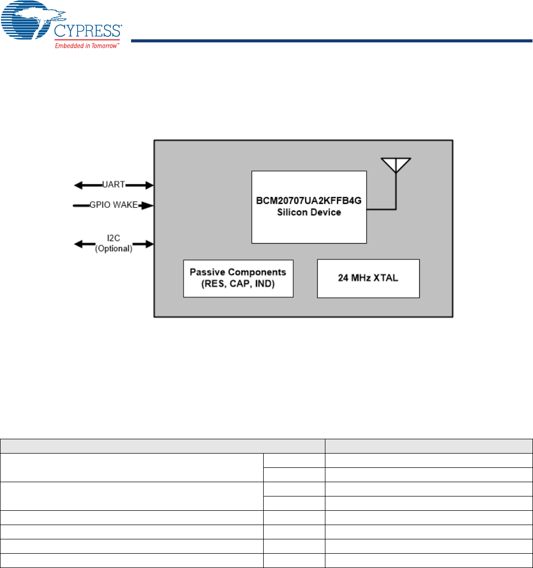
Overview
Functional Block Diagram
Figure 1 illustrates the CYBT-013033-01 functional block diagram.
Figure 1. Functional Block Diagram
Module Description
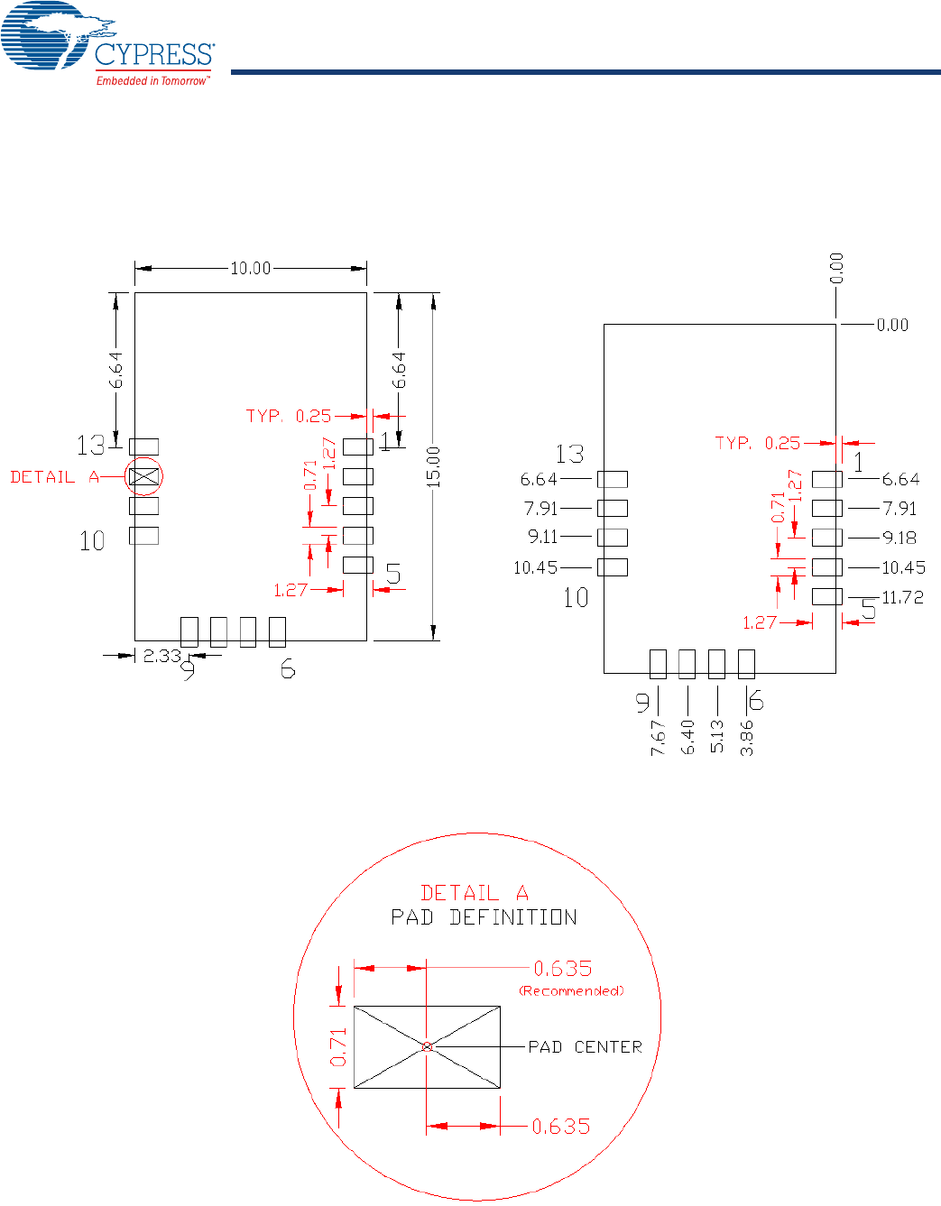
The CYBT-013033-01 module is a complete module designed to be soldered to the applications main board.
Module Dimensions and Drawing
Cypress reserves the right to select components from various vendors to achieve the Bluetooth module functionality. Such selections
will still guarantee that all mechanical specifications and module certifications are maintained. Designs should be held within the
physical dimensions shown in the mechanical drawings in Figure 2 on page 4. All dimensions are in millimeters (mm).
Table 1. Module Design Dimensions
See Figure 2 for the mechanical reference drawing for CYBT-013033-01.
Dimension Item Specification
Module dimensions Length (X) 10.00 ± 0.15 mm
Width (Y) 15.00 ± 0.15 mm
Antenna location dimensions Length (X) 5.13 mm
Width (Y) 10.00 mm
PCB thickness Height (H) 0.80 ± 0.10 mm
Shield height Height (H) 1.45 ± 0.10 mm
Maximum component height Height (H) 1.05 mm typical (Bluetooth silicon device)
Total module thickness (bottom of module to highest component) Height (H) 2.25 mm typical
Document Number: 002-18414 Rev. ** Page 4 of 33
PRELIMINARY CYBT-013033-01
Figure 2. Module Mechanical Drawing
Bottom View (Seen from Bottom)
Side View
Top View (See from Top)
Notes
1. No metal should be located beneath or above the antenna area. Only bare PCB material should be located beneath the antenna area. For more information on
recommended host PCB layout, see “Recommended Host PCB Layout” on page 7.
2. The CYBT-013033-01 includes castellated pad connections, denoted as the circular openings at the pad location above. Refer to the 3D rendering in Figure 3 on
page 5 for a depiction of the pad construction.
Document Number: 002-18414 Rev. ** Page 5 of 33
PRELIMINARY CYBT-013033-01
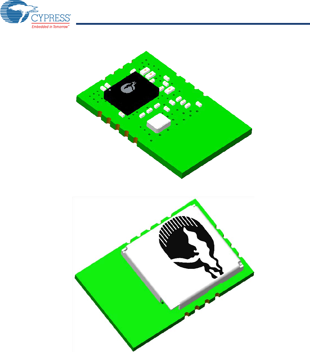
Figure 3. Module 3D Drawing
Top View With Shield
Top View Without Shield
Document Number: 002-18414 Rev. ** Page 6 of 33
PRELIMINARY CYBT-013033-01
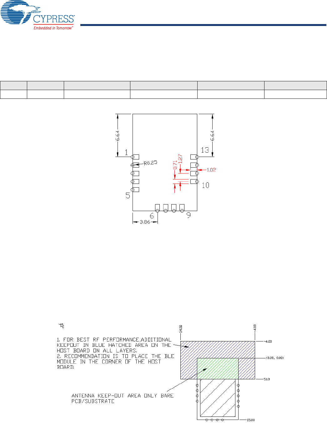
Pad Connection Interface
As shown in the bottom view of Figure 2 on page 4, the CYBT-013033-01 connects to the host board via solder pads on the bottom
side of the module. Table 2 and Figure 4 detail the solder pad length, width, and pitch dimensions of the CYBT-013033-01 module.
Figure 4. Solder Pad Dimensions (Seen from Bottom)
To maximize RF performance, the host layout should follow these recommendations:
1. Antenna Area Keepout: The host board directly below the antenna area of the Cypress module (see Figure 2 on page 4) must
contain no ground or signal traces. This keep out area requirement applies to all layers of the host board.
2. Module Placement: The ideal placement of the Cypress Bluetooth module is in a corner of the host board with the PCB trace
antenna located at the far corner. This placement minimizes the additional recommended keep out area stated in item 2. Please
refer to AN96841 for module placement best practices.
3. Optional Keepout: To maximize RF performance, the area immediately around the Cypress Bluetooth module PCB trace antenna
may contain an additional keep out area, where no grounding or signal traces are contained. The keep out area applies to all layers
of the host board. The recommended dimensions of the host PCB keep out area are shown in Figure 5 (dimensions are in mm).
Figure 5. Optional Additional Host PCB Keep Out Area Around the CYBT-013033-01 PCB Trace Antenna
Table 2. Solder Pad Connection Description
Name Connections Connection Type Pad Length Dimension Pad Width Dimension Pad Pitch
SP 13 Castellated Solder Pads 1.02 mm 0.71 mm 1.27 mm
Bottom View (Seen from Bottom)
Optional Host PCB Keep Out Area Around Chip Antenna
Document Number: 002-18414 Rev. ** Page 7 of 33
PRELIMINARY CYBT-013033-01
Recommended Host PCB Layout
Figure 6 (Dimensioned) and Figure 7 (Relative to Origin) provide the recommended host PCB layout pattern for the CYBT-013033-01.
Pad length of 1.27 mm (0.655 mm from center of the pad on either side) shown in Figure 7 is the minimum recommended host pad
length. All dimensions are in millimeters.
Figure 6. CYBT-013033-01 Host Layout (Dimensioned) Figure 7. CYBT-013033-01 Host Layout (Relative to Origin)
Top View (Seen on Host PCB)
Top View (Seen on Host PCB)
Figure 8. Solder Pad Reference Dimensions

Document Number: 002-18414 Rev. ** Page 8 of 33
PRELIMINARY CYBT-013033-01
Module Connections
Table 3 details the solder pad connection definitions and available functions for each connection pad. Table 3 lists the solder pads on
the CYBT-013033-01, the silicon device pin, and denotes what functions are available for each solder pad. Table 3 also lists the
primary/intended function for each solder pad for the application this module was specifically designed for.
Connections and Optional External Components
Power Connections (VDDIN)
The CYBT-013033-01 contains one power supply connection,
VDDIN.
VDDIN accepts a supply range of 3.00 V to 3.60 V. Table 10
provides this specification. The maximum power supply ripple for
this power connection is 100 mV, as shown in Table 10.
External Reset (XRES)
The CYBT-013033-01 has an integrated power-on reset circuit
which completely resets all circuits to a known power on state.
This action can also be driven by an external reset signal, which
can be used to externally control the device, forcing it into a
power-on reset state. The XRES signal is an active-low signal,
which is an input to the CYBT-013033-01 module.
UART Connections
For full UART functionality, all UART signals must be connected
to the Host device. If full UART functionality is not being used,
and only UART RXD and TXD are desired or capable, then the
following connection considerations should be followed for
UART RTS and CTS:
■UART RTS: Can be left floating, pulled low, or pulled high. RTS
is not critical for initial firmware uploading at power on.
■UART CTS: Must by pulled low to bypass flow control and to
ensure that continuous data transfers are made from the host
to the module.
External Component Recommendation
Power Supply Circuitry
It is not required to place any power supply decoupling or noise
reduction circuitry on the host PCB. If desired, an external ferrite
bead between the supply and the module connection can be
included, but is not necessary. If used, the ferrite bead should be
positioned as close as possible to the module pin connection.
If used, the recommended ferrite bead value is 330, 100 MHz.
(Murata BLM21PG331SN1D).
Apple MFi Authentication Coprocessor Interface
If solder pads 2 and 3 are used as the interface to the Apple MFi
authentication coprocessor, 10 K pull-up resistors should be
placed between the MFi coprocessor and the Cypress module.
Table 3. Solder Pad Connection Definitions
Pad
Number Silicon
Device Pin UART BSC (I2C) PWM GPIO_WAKE GPIO Primary Function
1 A6 External Reset Hardware Connection Input External Reset (Active Low)
2A8 ✓(SCL) ✓(PWM3) ✓(P3, P29, or P35) Apple SCL Interface
3C7 ✓(SDA) ✓(PWM3) ✓(P12) Apple SDA Interface
4F8 ✓(BT_GPIO_0)[3] ✓(P36 or P38) Device Wake Event Input
5F7✓(PUART: RXD or TXD) ✓(BT_GPIO_1)[4] ✓(P25 or P32) UART_TX Debug
Host Wake Event Output
NC/GPIO
6F5 ✓(UART_RXD) UART RXD
7G4 ✓(UART_CTS) UART CTS
8F4 ✓(UART_TXD) UART TXD
9F3 ✓(UART_RTS) UART RTS
10 VDDIN Power Supply Input (3.00 to 3.60V) Power Supply Input
11 GND GND Ground Connection
12 GND GND Ground Connection
13 GND GND Ground Connection
Notes
3. BT_GPIO_0/BT_DEV_WAKE is a signal from the host to the CYBT-013033-01 that the host requires attention.
4. BT_GPIO_1/BT_HOST_WAKE is a signal from the CYBT-013033-01 module to the host indicating that the Bluetooth device requires attention.

Document Number: 002-18414 Rev. ** Page 10 of 33
PRELIMINARY CYBT-013033-01
Critical Components List
Table 4 details the critical components used in the CYBT-013033-01 module.
Table 4. Critical Component List
Antenna Design
Table 5 details the PCB trace antenna used in the CYBT-013033-01 module.
Table 5. Trace Antenna Specifications
Component Reference Designator Description
Silicon U1 49-pin BGA Dual-Mode BT/BLE Silicon Device - BCM20707UA2KFFB4G
Crystal Y1 24.000 MHz, 12PF
Item Description
Frequency Range 2400 – 2500 MHz
Peak Gain 0.5 dBi typical
Return Loss 10 dB minimum

Document Number: 002-18414 Rev. ** Page 11 of 33
PRELIMINARY CYBT-013033-01
Bluetooth Baseband Core
The Bluetooth Baseband Core (BBC) implements all of the time critical functions required for high-performance Bluetooth operation.
The BBC manages the buffering, segmentation, and routing of data for all connections. It also buffers data that passes through it,
handles data flow control, schedules SCO/ACL TX/RX transactions, monitors Bluetooth® slot usage, optimally segments and
packages data into baseband packets, manages connection status indicators, and composes and decodes HCI packets. In addition
to these functions, it independently handles HCI event types and HCI command types.
The following transmit and receive functions are also implemented in the BBC hardware to increase reliability and security of the
TX/RX data before sending over the air:
Symbol timing recovery, data deframing, forward error correction (FEC), header error control (HEC), cyclic redundancy check (CRC),
data decryption, and data dewhitening in the receiver.
Data framing, FEC generation, HEC generation, CRC generation, key generation, data encryption, and data whitening in the trans-
mitter.
Bluetooth Low Energy
The CYBT-013033-01 supports dual-mode Bluetooth (BR/EDR/BLE) operation. The CYBT-013033-01 supports all Bluetooth 4.2 and
legacy features, with the following benefits:
■Dual-mode Bluetooth (BR/EDR/BLE)
■Extended inquiry response (EIR): Shortens the time to retrieve the device name, specific profile, and operating mode.
■Encryption pause resume (EPR): Enables the use of Bluetooth® technology in a much more secure environment.
■Sniff subrating (SSR): Optimizes power consumption for low duty cycle asymmetric data flow, which subsequently extends battery life.
■Secure simple pairing (SSP): Reduces the number of steps for connecting two devices, with minimal or no user interaction required.
■Link supervision time out (LSTO): Additional commands added to HCI and Link Management Protocol (LMP) for improved link
timeout supervision.
■Quality of Service (QoS) enhancements: Changes to data traffic control, which results in better link performance. Audio, human
interface device (HID), bulk traffic, SCO, and enhanced SCO (eSCO) are improved with the erroneous data (ED) and packet boundary
flag (PBF) enhancements.
■Secure connections (BR/EDR)
■Fast advertising interval
■Piconet clock adjust
■Connectionless broadcast
■LE privacy v1.1
■Low duty cycle directed advertising
■LE dual mode topology
Link Control Layer
The link control layer is part of the Bluetooth link control functions that are implemented in dedicated logic in the link control unit (LCU).
This layer consists of the command controller that takes commands from the software, and other controllers that are activated or
configured by the command controller, to perform the link control tasks. Each task performs a different state in the Bluetooth® Link
Controller.
■Major states:
❐Standby
❐Connection
■Substates:
❐Page
❐Page Scan
❐Inquiry
❐Inquiry Scan
❐Sniff

Document Number: 002-18414 Rev. ** Page 12 of 33
PRELIMINARY CYBT-013033-01
Power Management Unit
The Power Management Unit (PMU) provides power management features that can be invoked through power management registers
or packet handling in the baseband core. This section contains descriptions of the PMU features.
RF Power Management
The BBC generates power-down control signals for the transmit path, receive path, PLL, and power amplifier to the 2.4 GHz trans-
ceiver. The transceiver then processes the power-down functions, accordingly.
SoC Power Management
The host can place the device in a sleep state, in which all nonessential blocks are powered off and all nonessential clocks are
disabled. Power to the digital core is maintained so that the state of the registers and RAM is not lost. In addition, the CYBT-013033-01
internal LPO clock is applied to the internal sleep controller so that the chip can wake automatically at a specified time or based on
signaling from the host. The goal is to limit the current consumption to a minimum, while maintaining the ability to wake up and resume
a connection with minimal latency.
If a scan or sniff session is enabled while the device is in Sleep mode, the device automatically will wake up for the scan/sniff event,
then go back to sleep when the event is done. In this case, the device uses its internal LPO-based timers to trigger the periodic wake
up. While in Sleep mode, the transports are idle. However, the device can wake up at any time. If signaled to wake up while a scan
or sniff session is in progress, the session continues but the device will not sleep between scan/sniff events. Once Sleep mode is
enabled, the wake signaling mechanism can also be thought of as a sleep signaling mechanism, since removing the wake status will
often cause the device to sleep.
In addition to a Bluetooth device wake signaling mechanism, there is a host wake signaling mechanism. This feature provides a way
for the Bluetooth device to wake up a host that is in a reduced power state.
Table 6 and Table 7 describe the mechanism available for the device and the host to signal a wake status to each other.
Table 6. Mechanism for Device and Host to Signal Wake Status
Bluetooth Baseband Core Power Management
The following are low-power operations for the Bluetooth Baseband Core (BBC):
■Physical layer packet-handling turns the RF on and off dynamically within transmit/receive packets.
■Bluetooth-specified low-power connection modes: sniff, hold, and park. While in these modes, the CYBT-013033-01 runs on the
low-power oscillator and wakes up after a predefined time period.
Bluetooth device WAKE (BT_DEV_WAKE - Pad 4) and
Host WAKE (and BT_HOST_WAKE - Pad 5) signaling The BT_DEV_WAKE signal allows the host to wake the BT device, and
BT_HOST_WAKE is an output that allows the BT device to wake the host.
Table 7. Power Control Pad Summary
Pin Name
(Pad Number) Direction Description
BT_DEV_WAKE
(Pad 4) Host output
BT input
Bluetooth device wake-up: Signal from the host to the Bluetooth device that the host requires
attention.
■Asserted = Bluetooth device must wake up or remain awake.
■Deasserted = Bluetooth device may sleep when sleep criteria are met.
The polarity of this signal is software configurable and can be asserted high or low. By
default, BT_DEV_WAKE is active-low (if BT-WAKE is low it requires the device to wake up
or remain awake).
BT_HOST_WAKE
(Pad 5) BT output
Host input
Host wake-up. Signal from the Bluetooth device to the host indicating that Bluetooth device
requires attention.
■Asserted = Host device must wake up or remain awake.
■Deasserted = Host device may sleep when sleep criteria are met.
The polarity of this signal is software configurable and can be asserted high or low.
XRES (Pad 1) BT input Used to place the chip in reset. XRES is active-low.

Document Number: 002-18414 Rev. ** Page 13 of 33
PRELIMINARY CYBT-013033-01
Adaptive Frequency Hopping
The CYBT-013033-01 supports host channel classification and dynamic channel classification Adaptive Frequency Hopping (AFH)
schemes, as defined in the Bluetooth specification.
Host channel classification enables the host to set a predefined hopping map for the device to follow.
If dynamic channel classification is enabled, the device gathers link quality statistics on a channel-by-channel basis to facilitate channel
assessment and channel map selection. To provide a more accurate frequency hop map, link quality is determined using both RF and
baseband signal processing.

Document Number: 002-18414 Rev. ** Page 14 of 33
PRELIMINARY CYBT-013033-01
Microprocessor Unit
Overview
The CYBT-013033-01 microprocessor unit runs software from the Link Control (LC) layer up to the stack and Application layer. In the
HCI mode of operation the stack will be run on the external host. The microprocessor is based on the Cortex-M3 32-bit RISC processor
with embedded ICE-RT debug and JTAG interface units. The microprocessor also includes 848 KB of ROM memory for program
storage and boot ROM, 352 KB of RAM for data scratch-pad, and patch RAM code.
The internal boot ROM provides flexibility during power-on reset to enable the same device to be used in various configurations,
including automatic host transport selection from UART transport without external NVRAM. At power-up, the lower layer protocol stack
is executed from the internal ROM.
External patches can be applied to the ROM-based firmware to provide flexibility for bug fixes and features additions. These patches
can be downloaded from the host to the device through the UART transport.
One-Time Programmable Memory
The CYBT-013033-01 includes a One-Time Programmable (OTP) memory, allowing manufacturing customization and avoiding the
need for an on-board NVRAM. If customization is not required, then the OTP does not need to be programmed. Whether the OTP is
programmed or not, it is disabled after the boot process completes to save power.
The OTP size is 2048 bytes.
The OTP is designed to store a minimal amount of information. Aside from OTP data, most user configuration information will be
downloaded into RAM after the CYBT-013033-01 boots up and is ready for host transport communication. The OTP contents are
limited to:
■Parameters required prior to downloading user configuration to RAM.
■Parameters unique to each part and each customer (i.e., the BD_ADDR, and software license key).
The following are typical parameters programmed into the OTP memory:
■BD_ADDR
■Software license key
■Output power calibration
■Frequency trimming
■Initial status LED drive configuration
The OTP contents also include a static error correction table to improve yield during the programming process as well as forward error
correction codes to eliminate any long-term reliability problems. The OTP contents associated with error correction are not visible by
customers.
Peripheral Transport Unit
This section discusses the UART peripheral interface. The CYBT-013033-01 has a 1040-byte transmit and receive FIFO, which is
large enough to hold the entire payload of the largest EDR Bluetooth packet (3-DH5).
HCI Transport Detection Configuration
Note: HCI transport detection is only valid for the HCI operating mode.
The CYBT-013033-01 supports the following interface types for the HCI transport from the host:
■UART (H4)
Only one host interface can be active at a time. The firmware performs a transport detect function at boot-time to determine which
host is the active transport. It can auto-detect UART interfaces, but the SPI interface must be selected by strapping the SCL pin to 0.
■The complete algorithm is summarized as follows:
■Determine if any local NVRAM contains a valid configuration file. If it does and a transport configuration entry is present, select the
active transport according to entry, and then exit the transport detection routine.
■Look for CTS_N = 0 on the UART interface. If it is present, select UART.
■Repeat Step 2 and Step 3 until transport is determined.

Document Number: 002-18414 Rev. ** Page 15 of 33
PRELIMINARY CYBT-013033-01
UART Interface
The CYBT-013033-01 shares a single UART for Bluetooth. The UART is a standard 4-wire interface (RX, TX, RTS, and CTS) with
adjustable baud rates from 9600 bps to 4.0 Mbps. The interface features an automatic baud rate detection capability that returns a
baud rate selection. Alternatively, the baud rate may be selected through a vendor-specific UART HCI command.
UART has a 1040-byte receive FIFO and a 1040-byte transmit FIFO to support EDR. Access to the FIFOs is conducted through the
AHB interface through either DMA or the CPU. The UART supports the Bluetooth 4.2 UART HCI specification: H4, and a custom
Extended H4. The default baud rate is 115.2 Kbaud.
The CYBT-013033-01 UART can perform XON/XOFF flow control and includes hardware support for the Serial Line Input Protocol
(SLIP). It can also perform wake-on activity. For example, activity on the RX or CTS inputs can wake the chip from a sleep state.
Normally, the UART baud rate is set by a configuration record downloaded after device reset, or by automatic baud rate detection,
and the host does not need to adjust the baud rate. Support for changing the baud rate during normal HCI UART operation is included
through a vendor-specific command that allows the host to adjust the contents of the baud rate registers. The CYBT-013033-01 UARTs
operate correctly with the host UART as long as the combined baud rate error of the two devices is within ±2%.
Table 8. Example of Common Baud Rates
Desired Rate Actual Rate Error (%)
4000000 4000000 0.00
3692000 3692308 0.01
3000000 3000000 0.00
2000000 2000000 0.00
1500000 1500000 0.00
1444444 1454544 0.70
921600 923077 0.16
460800 461538 0.16
230400 230796 0.17
115200 115385 0.16
57600 57692 0.16
38400 38400 0.00
28800 28846 0.16
19200 19200 0.00
14400 14423 0.16
9600 9600 0.00

Document Number: 002-18414 Rev. ** Page 16 of 33
PRELIMINARY CYBT-013033-01
Electrical Characteristics
Note: All voltages listed in Table 9 are referenced to VDDIN.
Table 9. Absolute Maximum Voltage
Requirement Parameter Specification Units
Minimum Nominal Maximum
Ambient Temperature of Operation –30 25 85 °C
Storage temperature –40 – 150 °C
VDD Core 1.14 1.2 1.26 V
VDD IO 3 3.3 3.6 V
VDD RF (excluding class 1 PA) 1.14 1.2 1.26 V
VDD PA (class 1 mode) 2.25 2.5 2.75 V
Table 10. Power Supply Specifications
Parameter Min. Typ. Max. Units Comments
VDDIN input 3.0 3.3 3.6 V –
VDDIN_Ripple – – 100 mV 3.0V supply
Ripple frequency of 100 kHz to 750 kHz
VBAT input 3.0 3.3 3.6 V Internally routed on CYBT-013033-01 module
2.5V LDO input 3.0 3.3 3.6 V Internally routed on CYBT-013033-01 module
Table 11. VDDC LDO Electrical Specifications
Parameter Conditions Min. Typ. Max. Units
Input Voltage – 1.62 3.3 3.6 V
Nominal Output
Voltage ––1.2–V
DC Accuracy Accuracy at any step, including bandgap reference. –5 – 5 %
Output Voltage
Programmability
Range 0.89 – 1.34 V
Step Size –30–mV
Load Current – – – 40 mA
Dropout Voltage Iload = 40 mA – – 200 mV
Line Regulation Vin from 1.62V to 3.6V, Iload = 40 mA – – 0.2 %Vo/V
Load Regulation Iload = 1 mA to 40 mA, Vout = 1.2V, Package + PCB
R = 0.3W – 0.02 0.05 %Vo/mA
Quiescent Current No load @Vin = 3.3V – 18 23 A
Max load @Vin = 3.3V – – 0.56 0.65 mA
Power Down Current Vin = 3.3V @25C – 0.2 – A
PSRR Vin = 3.3, Vout = 1.2V,
Iload = 40 mA
1 kHz 65 – – dB
10 kHz 60 – – dB
100 kHz 55 – – dB
Over Current Limit – 100 – – mA
Turn-on Time VBAT = 3.3V, BG already on, LDO OFF to ON,
Co = 1 F, 90% of Vout – – 100 s

Document Number: 002-18414 Rev. ** Page 17 of 33
PRELIMINARY CYBT-013033-01
External Output
Capacitor Ceramic cap with ESR 0.50.814.7F
External Input
Capacitor Ceramic, X5R, 0402, ±20%, 10V. – 1 – F
Turn-on Time VBAT = 3.3V, BG already on, LDO OFF to ON,
Co = 1 F, 90% of Vout – – 100 s
Table 12. BTLDO_2P5 Electrical Specifications
Parameters Conditions Min Typ Max Units
Input supply voltage,
Vin
Min = Vo + 0.2V = 2.7V
(for Vo = 2.5V)
Dropout voltage requirement must be met
under maximum load for performance
specs.
3.0 3.3 3.6 V
Nominal output voltage,
Vo Default = 2.5V – 2.5 – V
Output voltage
programmability
Range
Accuracy at any step (including line/load
regulation), load >0.1 mA
2.2
–5 –2.8
5V
%
Dropout voltage At max load – – 200 mV
Output current – 0.1 – 70 mA
Quiescent current No load; Vin = Vo + 0.2V
Max load @ 70 mA; Vin = Vo + 0.2V –8
660 16
700 A
Leakage current Power-down mode. At junction temperature
85°C. –1.55A
Line regulation Vin from (Vo + 0.2V) to 3.6V, max load – – 3.5 mV/V
Load regulation Load from 1 mA to 70 mA, Vin = 3.6V – – 0.3 mV/mA
PSRR Vin Vo + 0.2V, Vo = 2.5V, Co = 2.2 F,
max load, 100 Hz to 100 kHz 20 – – dB
LDO turn-on time LDO turn-on time when rest of chip is up – – 150 s
Table 13. Digital I/O Characteristics
Characteristics Symbol Minimum Typical Maximum Unit
Input low voltage (VDDIN = 3.3V) VIL ––0.8V
Input high voltage (VDDIN = 3.3V) VIH 2.0 – – V
Output low voltage VOL ––0.4V
Output high voltage VOH VDDIN – 0.4V – – V
Input low current IIL ––1.0A
Input high current IIH ––1.0A
Output low current (VDDIN = 3.3V, VOL = 0.4V) IOL ––2.0mA
Output high current (VDDIN = 3.3V, VOH = 2.9V) IOH ––4.0mA
Input capacitance CIN ––0.4pF
Table 11. VDDC LDO Electrical Specifications (continued)
Parameter Conditions Min. Typ. Max. Units

Document Number: 002-18414 Rev. ** Page 18 of 33
PRELIMINARY CYBT-013033-01
Table 14. Current Consumption — Common Use Cases
Condition Current (mA)
Receive (1 Mbps) current level when receiving a basic rate packet. 12.5
Transmit (1 Mbps) current level when transmitting a basic rate packet. 26.5
Receive (EDR) current level when receiving a 2 or 3 Mbps rate packet. 12.5
Transmit (EDR) current level when transmitting a 2 or 3 Mbps rate packet. 20.0
DM1/DH1 average current during a basic rate maximum throughput connection that includes only this packet type. 14.5
DM3/DH3 average current during a basic rate maximum throughput connection that includes only this packet type. 17.0
DM5/DH5 average current during a maximum basic rate throughput connection that includes only this packet type. 17.5
Sleep UART transport active. External LPO clock available. 0.120
Inquiry Scan (1.28 sec.). Periodic scan rate is 1.28 sec. 0.188
Page Scan (R1) Periodic scan rate is R1 (1.28 sec). 0.188
Inquiry Scan + Page Scan (R1)
Both inquiry and page scans are interlaced together at a 1.28 seconds periodic scan rate. 0.286
Sniff master (500 ms) attempt and timeout parameters set to 4. Quality connection that rarely requires more than
a minimum packet exchange. 0.415
Sniff slave (500 ms) attempt and timeout parameters set to 4. Quality connection that rarely requires more than a
minimum packet exchange. 0.408
Sniff (500 ms) + Inquiry or Page Scan (R1) 0.700
Sniff (500ms) + Inquiry Scan + Page Scan (R1) 0.800

Document Number: 002-18414 Rev. ** Page 19 of 33
PRELIMINARY CYBT-013033-01
RF Specifications
Table 15. Receiver RF Specifications[5, 6]
Parameter Conditions Minimum Typical[7] Maximum Unit
General
Frequency range – 2402 – 2480 MHz
RX sensitivity[8] GFSK, 0.1% BER, 1 Mbps – –93.5 – dBm
p/4-DQPSK, 0.01% BER, 2 Mbps – –95.5 – dBm
8-DPSK, 0.01% BER, 3 Mbps – –89.5 – dBm
Maximum input GFSK, 1 Mbps – – –20 dBm
Maximum input p/4-DQPSK, 8-DPSK, 2/3 Mbps – – –20 dBm
Interference Performance
■GFSK Modulation[9]
C/I cochannel GFSK, 0.1% BER – 9.5 11 dB
C/I 1 MHz adjacent channel GFSK, 0.1% BER – –5 0 dB
C/I 2 MHz adjacent channel GFSK, 0.1% BER – –40 –30.0 dB
C/I > 3 MHz adjacent channel GFSK, 0.1% BER – –49 –40.0 dB
C/I image channel GFSK, 0.1% BER – –27 –9.0 dB
C/I 1 MHz adjacent to image channel GFSK, 0.1% BER – –37 –20.0 dB
■QPSK Modulation[10]
C/I cochannel p/4-DQPSK, 0.1% BER – 11 13 dB
C/I 1 MHz adjacent channel p/4-DQPSK, 0.1% BER – –8 0 dB
C/I 2 MHz adjacent channel p/4-DQPSK, 0.1% BER – –40 –30.0 dB
C/I > 3 MHz adjacent channel 8-DPSK, 0.1% BER – –50 –40.0 dB
C/I image channel p/4-DQPSK, 0.1% BER – –27 –7.0 dB
C/I 1 MHz adjacent to image channel p/4-DQPSK, 0.1% BER – –40 –20.0 dB
■8PSK Modulation[11]
C/I cochannel 8-DPSK, 0.1% BER – 17 21 dB
C/I 1 MHz adjacent channel 8-DPSK, 0.1% BER – –5 5 dB
C/I 2 MHz adjacent channel 8-DPSK, 0.1% BER – –40 –25.0 dB
C/I > 3 MHz adjacent channel 8-DPSK, 0.1% BER – –47 –33.0 dB
C/I Image channel 8-DPSK, 0.1% BER – –20 0 dB
C/I 1 MHz adjacent to image channel 8-DPSK, 0.1% BER – –35 –13.0 dB
Notes
5. All specifications are single ended. Unused inputs are left open.
6. All specifications, except typical, are for industrial temperatures.
7. Typical operating conditions are 3.3V VBAT and 25°C ambient temperature.
8. The receiver sensitivity is measured at BER of 0.1% on the device interface.
9. Typical GFSK CI numbers at –7 MHz, –5 MHz, and –3 MHz are –45 dB, –42 dB, and –41 dB, respectively.
10. Typical QPSK CI numbers at –7 MHz, –5 MHz, and –3 MHz are –46 dB, –43 dB, and –42 dB, respectively.
11. Typical 8PSK CI numbers at –7 MHz, –5 MHz, and –3 MHz are –50 dB, –45 dB, and –45 dB, respectively.
12. Meets this specification using front-end band pass filter.
13. Numbers are referred to the pin output with an external BPF filter.
14. f0 = -64 dBm Bluetooth-modulated signal, f1 = –39 dBm sine wave, f2 = –39 dBm Bluetooth-modulated signal, f0 = 2f1 – f2, and |f2 – f1| = n * 1 MHz, where “n” is 3,
4, or 5. For the typical case, n = 4.
15. Includes baseband radiated emissions.

Document Number: 002-18414 Rev. ** Page 20 of 33
PRELIMINARY CYBT-013033-01
Out-of-Band Blocking Performance (CW)[12]
30 MHz–2000 MHz 0.1% BER – –10.0 – dBm
2000–2399 MHz 0.1% BER – –27 – dBm
2498–3000 MHz 0.1% BER – –27 – dBm
3000 MHz–12.75 GHz 0.1% BER – –10.0 – dBm
Out-of-Band Blocking Performance, Modulated Interferer
776–764 MHz CDMA – –10[13] –dBm
824–849 MHz CDMA – –10[13] –dBm
1850–1910 MHz CDMA – –23[13] –dBm
824–849 MHz EDGE/GSM – –10[13] –dBm
880–915 MHz EDGE/GSM – –10[13] –dBm
1710–1785 MHz EDGE/GSM – –23[13] –dBm
1850–1910 MHz EDGE/GSM – –23[13] –dBm
1850–1910 MHz WCDMA – –23[13] –dBm
1920–1980 MHz WCDMA – –23[13] –dBm
Intermodulation Performance[14]
BT, Df = 4 MHz – –39.0 – – dBm
Spurious Emissions[15]
30 MHz to 1 GHz – – – –62 dBm
1–12.75 GHz – – – –47 dBm
65–108 MHz FM RX – –147 – dBm/Hz
746–764 MHz CDMA – –147 – dBm/Hz
851–894 MHz CDMA – –147 – dBm/Hz
925–960 MHz EDGE/GSM – –147 – dBm/Hz
1805–1880 MHz EDGE/GSM – –147 – dBm/Hz
1930–1990 MHz PCS – –147 – dBm/Hz
2110–2170 MHz WCDMA – –147 – dBm/Hz
Table 15. Receiver RF Specifications[5, 6] (continued)
Parameter Conditions Minimum Typical[7] Maximum Unit
Notes
5. All specifications are single ended. Unused inputs are left open.
6. All specifications, except typical, are for industrial temperatures.
7. Typical operating conditions are 3.3V VBAT and 25°C ambient temperature.
8. The receiver sensitivity is measured at BER of 0.1% on the device interface.
9. Typical GFSK CI numbers at –7 MHz, –5 MHz, and –3 MHz are –45 dB, –42 dB, and –41 dB, respectively.
10. Typical QPSK CI numbers at –7 MHz, –5 MHz, and –3 MHz are –46 dB, –43 dB, and –42 dB, respectively.
11. Typical 8PSK CI numbers at –7 MHz, –5 MHz, and –3 MHz are –50 dB, –45 dB, and –45 dB, respectively.
12. Meets this specification using front-end band pass filter.
13. Numbers are referred to the pin output with an external BPF filter.
14. f0 = -64 dBm Bluetooth-modulated signal, f1 = –39 dBm sine wave, f2 = –39 dBm Bluetooth-modulated signal, f0 = 2f1 – f2, and |f2 – f1| = n * 1 MHz, where “n” is 3,
4, or 5. For the typical case, n = 4.
15. Includes baseband radiated emissions.

Document Number: 002-18414 Rev. ** Page 21 of 33
PRELIMINARY CYBT-013033-01
Notes
16. All specifications are for industrial temperatures.
17. All specifications are single-ended. Unused input are left open.
18. +12 dBm output for GFSK measured with PA VDD = 2.5V.
19. +9 dBm output for EDR measured with PA VDD = 2.5V.
20. Maximum value is the value required for Bluetooth qualification.
21. Meets this spec using a front-end bandpass filter.
Table 16. Transmitter RF Specifications[16,17]
Parameter Conditions Minimum Typical Maximum Unit
General
Frequency range – 2402 – 2480 MHz
Class1: GFSK TX power[18] ––12–dBm
Class1: EDR TX power[19] – –9–dBm
Class 2: GFSK TX power – – 2 – dBm
Power control step – 2 4 8 dB
Modulation Accuracy
p/4-DQPSK Frequency Stability – –10 – 10 kHz
p/4-DQPSK RMS DEVM – – – 20 %
p/4-QPSK Peak DEVM – – – 35 %
p/4-DQPSK 99% DEVM – – – 30 %
8-DPSK frequency stability – –10 – 10 kHz
8-DPSK RMS DEVM – – – 13 %
8-DPSK Peak DEVM – – – 25 %
8-DPSK 99% DEVM – – – 20 %
In-Band Spurious Emissions
1.0 MHz < |M – N| < 1.5 MHz – – – –26 dBc
1.5 MHz < |M – N| < 2.5 MHz – – – –20 dBm
|M – N| > 2.5 MHz – – – –40 dBm
Out-of-Band Spurious Emissions
30 MHz to 1 GHz – – – –36.0[20] dBm
1–12.75 GHz – – – –30.0[20,21] dBm
1.8–1.9 GHz – – – –47.0 dBm
5.15–5.3 GHz – – – –47.0 dBm
GPS Band Noise Emission (without a front-end band pass filter)
1572.92 MHz to 1577.92 MHz – – –150 –127 dBm/Hz
Out-of-Band Noise Emissions (without a front-end band pass filter)
65–108 MHz FM RX – –145 – dBm/Hz
746–764 MHz CDMA – –145 – dBm/Hz
869–960 MHz CDMA – –145 – dBm/Hz
925–960 MHz EDGE/GSM – –145 – dBm/Hz
1805–1880 MHz EDGE/GSM – –145 – dBm/Hz
1930–1990 MHz PCS – –145 – dBm/Hz
2110–2170 MHz WCDMA – –140 – dBm/Hz
Document Number: 002-18414 Rev. ** Page 22 of 33
PRELIMINARY CYBT-013033-01
Timing and AC Characteristics
In this section, use the numbers listed in the reference column to interpret the timing diagrams.
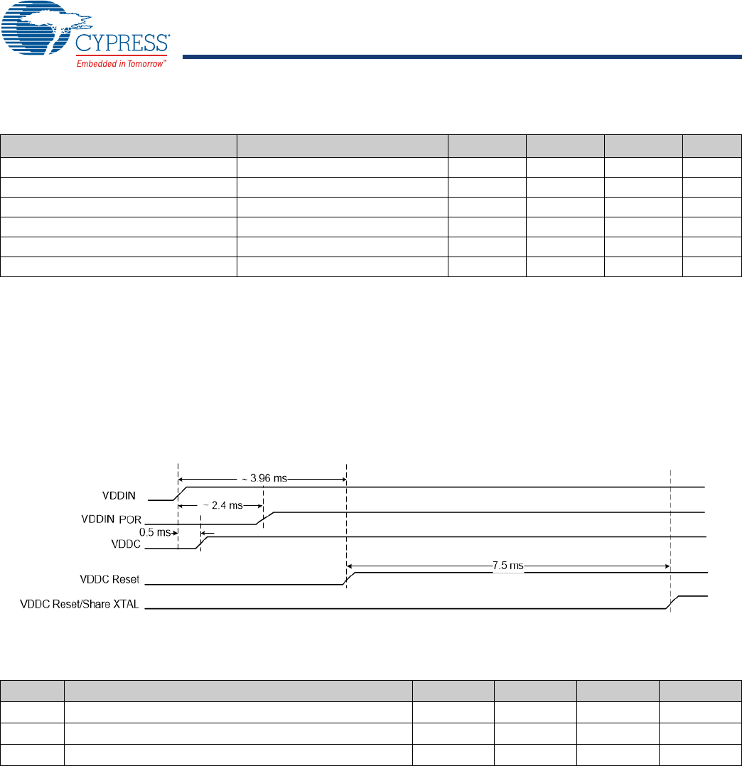
System Startup Timing
The global reset signal in the CYBT-013033-01 is a logical OR (actually a wired AND, since the signals are active low) of the XRES
input and the internal POR signals. The last signal to be released determines the time at which the chip is released from reset. The
POR is typically asserted for 2.4 ms after the POR threshold is crossed.
Figure 10 illustrates the startup timing for the CYBT-013033-01.
Figure 10. System Startup Timing
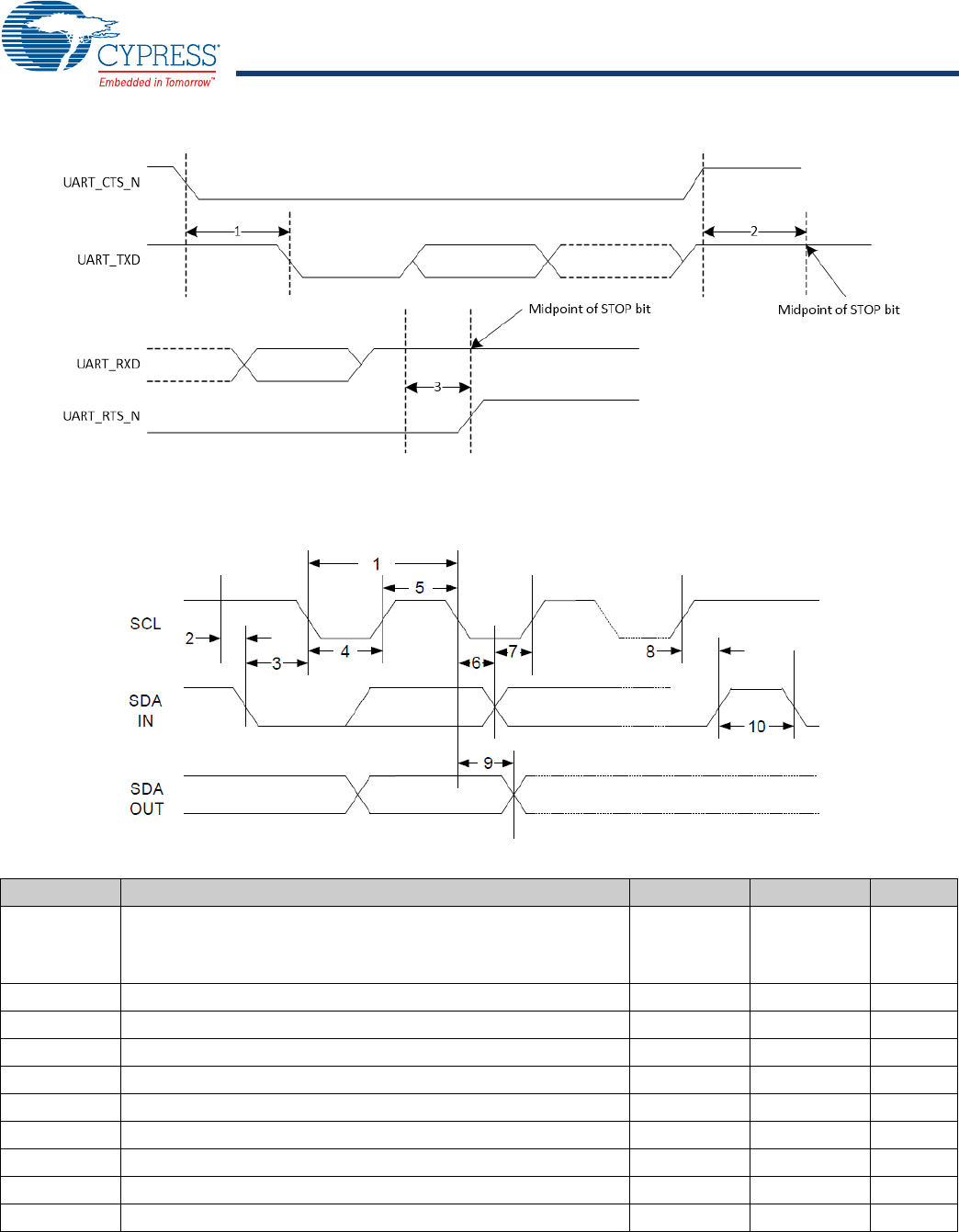
UART Timing
Table 17. BLE RF Specifications
Parameter Conditions Minimum Typical Maximum Unit
Frequency Range NA 2402 – 2480 MHz
RX Sense[22] GFSK, 0.1% BER, 1 Mbps – –96.5 – dBm
TX Power[23] NA – 9 – dBm
Mod Char: Delta F1 average NA 225 255 275 kHz
Mod Char: Delta F2 max[24] NA 99.9 – – %
Mod Char: Ratio NA 0.8 0.95 – %
Notes
22. Dirty TX is Off.
23. The BLE TX power can be increased to compensate for front-end losses such as BPF, diplexer, switch, etc. The output is capped at 12 dBm out. The BLE TX power
at the antenna port cannot exceed the 10 dBm EIRP specification limit.
24. At least 99.9% of all delta F2 max frequency values recorded over 10 packets must be greater than 185 kHz.
Table 18. UART Timing Specifications
Ref No. Characteristics Minimum Typical Maximum Unit
1 Delay time UART_CTS_N low to UART TXD valid. – – 1.50 Bit periods
2 Setup time UART_CTS_N high before midpoint of stop bit. – – 0.67 Bit periods
3 Delay time Midpoint of stop bit to UART_RTS_N high. – – 1.33 Bit periods
Document Number: 002-18414 Rev. ** Page 23 of 33
PRELIMINARY CYBT-013033-01
Figure 11. UART Timing
BSC Interface Timing
The timing intervals displayed in Figure 12 can be referenced in Table 19.
Figure 12. BSC Interface Timing Diagram
Table 19. BSC Interface Timing Specifications
Reference Characteristics Minimum Maximum Unit
1 Clock frequency –
100
400
800
1000
kHz
2 START condition setup time 650 – ns
3 START condition hold time 280 – ns
4 Clock low time 650 – ns
5 Clock high time 280 – ns
6 Data input hold time[25] 0–ns
7 Data input setup time 100 – ns
8 STOP condition setup time 280 – ns
9 Output valid from clock – 400 ns
10 Bus free time[26] 650 – ns
Notes
25. As a transmitter, 300 ns of delay is provided to bridge the undefined region of the falling edge of SCL to avoid unintended generation of START or STOP conditions
26. Time that the cbus must be free before a new transaction can start.
Document Number: 002-18414 Rev. ** Page 24 of 33
PRELIMINARY CYBT-013033-01
Environmental Specifications
Environmental Compliance
This Cypress BLE module is produced in compliance with the Restriction of Hazardous Substances (RoHS) directive. The Cypress
module and components used to produce this module are RoHS compliant.
RF Certification
The CYBT-013033-01 module is certified under the following RF certification standards:
■FCC: WAP3033
■CE
■IC: 7922A-3033
■MIC: TBD
Safety Certification
The CYBT-013033-01 module complies with the following safety regulations:
■Underwriters Laboratories, Inc. (UL): Filing E331901
■CSA
■TUV
Environmental Conditions
Table describes the operating and storage conditions for the Cypress BLE module.
ESD and EMI Protection
Exposed components require special attention to ESD and electromagnetic interference (EMI).
A grounded conductive layer inside the device enclosure is suggested for EMI and ESD performance. Any openings in the enclosure
near the module should be surrounded by a grounded conductive layer to provide ESD protection and a low-impedance path to ground.
Device Handling: Proper ESD protocol must be followed in manufacturing to ensure component reliability.
Table 20. Environmental Conditions for CYBT-013033-01
Description Minimum Specification Maximum Specification
Operating temperature 30 °C 85 °C
Operating humidity (relative, non-condensation) 5% 85%
Thermal ramp rate – 3 °C/minute
Storage temperature –30 °C 85 °C
Storage temperature and humidity – 85 °C at 85%
ESD: Module integrated into system Components[27] –15 kV Air
2.0 kV Contact
Note
27. This does not apply to the RF pins (ANT).

Document Number: 002-18414 Rev. ** Page 25 of 33
PRELIMINARY CYBT-013033-01
Regulatory Information
FCC
FCC NOTICE:
The device CYBT-013033-01 complies with Part 15 of the FCC Rules. The device meets the requirements for modular transmitter
approval as detailed in FCC public Notice DA00-1407.transmitter Operation is subject to the following two conditions: (1) This device
may not cause harmful interference, and (2) This device must accept any interference received, including interference that may cause
undesired operation.
CAUTION:
The FCC requires the user to be notified that any changes or modifications made to this device that are not expressly approved by
Cypress Semiconductor may void the user's authority to operate the equipment.
This equipment has been tested and found to comply with the limits for a Class B digital device, pursuant to Part 15 of the FCC Rules.
These limits are designed to provide reasonable protection against harmful interference in a residential installation. This equipment
generates uses and can radiate radio frequency energy and, if not installed and used in accordance with the instructions,ê may cause
harmful interference to radio communications. However, there is no guarantee that interference will not occur in a particular installation.
If this equipment does cause harmful interference to radio or television reception, which can be determined by turning the equipment
off and on, the user is encouraged to try to correct the interference by one or more of the following measures:
■Reorient or relocate the receiving antenna.
■Increase the separation between the equipment and receiver.
■Connect the equipment into an outlet on a circuit different from that to which the receiver is connected.
■Consult the dealer or an experienced radio/TV technician for help
LABELING REQUIREMENTS:
The Original Equipment Manufacturer (OEM) must ensure that FCC labelling requirements are met. This includes a clearly visible
label on the outside of the OEM enclosure specifying the appropriate Cypress Semiconductor FCC identifier for this product as well
as the FCC Notice above. The FCC identifier is FCC ID: WAP3033.
In any case the end product must be labeled exterior with “Contains FCC ID: WAP3033”.
ANTENNA WARNING:
This device is tested with a standard SMA connector and with the antennas listed below. When integrated in the OEMs product, these
fixed antennas require installation preventing end-users from replacing them with non-approved antennas. Any antenna not in the
following table must be tested to comply with FCC Section 15.203 for unique antenna connectors and Section 15.247 for emissions.
RF EXPOSURE:
To comply with FCC RF Exposure requirements, the Original Equipment Manufacturer (OEM) must ensure to install the approved
antenna in the previous.
The preceding statement must be included as a CAUTION statement in manuals, for products operating with the approved antennas
in Table 5 on page 10, to alert users on FCC RF Exposure compliance. Any notification to the end user of installation or removal
instructions about the integrated radio module is not allowed.
The radiated output power of CYBT-013033-01 with the chip antenna mounted (FCC ID: WAP3033 ) is far below the FCC radio frequency
exposure limits. Nevertheless, use CYBT-013033-01 in such a manner that minimizes the potential for human contact during normal
operation.
End users may not be provided with the module installation instructions. OEM integrators and end users must be provided with
transmitter operating conditions for satisfying RF exposure compliance.
Document Number: 002-18414 Rev. ** Page 26 of 33
PRELIMINARY CYBT-013033-01
Industry Canada (IC) Certification
CYBT-013033-01 is licensed to meet the regulatory requirements of Industry Canada (IC),
License: IC: 7922A-3033
Manufacturers of mobile, fixed or portable devices incorporating this module are advised to clarify any regulatory questions and ensure
compliance for SAR and/or RF exposure limits. Users can obtain Canadian information on RF exposure and compliance from
www.ic.gc.ca.
This device has been designed to operate with the antennas listed in Table 5 on page 10, having a maximum gain of 0.5 dBi. Antennas
not included in this list or having a gain greater than 0.5 dBi are strictly prohibited for use with this device. The required antenna
impedance is 50 ohms. The antenna used for this transmitter must not be co-located or operating in conjunction with any other antenna
or transmitter.
IC NOTICE:
The device CYBT-013033-01 including the built-in trace antenna complies with Canada RSS-GEN Rules. The device meets the
requirements for modular transmitter approval as detailed in RSS-GEN. Operation is subject to the following two conditions: (1) This
device may not cause harmful interference, and (2) This device must accept any interference received, including interference that
may cause undesired operation.
IC RADIATION EXPOSURE STATEMENT FOR CANADA
This device complies with Industry Canada licence-exempt RSS standard(s). Operation is subject to the following two conditions: (1)
this device may not cause interference, and (2) this device must accept any interference, including interference that may cause
undesired operation of the device.
Le présent appareil est conforme aux CNR d'Industrie Canada applicables aux appareils radio exempts de licence. L'exploitation est
autorisée aux deux conditions suivantes : (1) l'appareil ne doit pas produire de brouillage, et (2) l'utilisateur de l'appareil doit accepter
tout brouillage radioélectrique subi, même si le brouillage est susceptible d'en compromettre le fonctionnement.
LABELING REQUIREMENTS:
The Original Equipment Manufacturer (OEM) must ensure that IC labelling requirements are met. This includes a clearly visible label
on the outside of the OEM enclosure specifying the appropriate Cypress Semiconductor IC identifier for this product as well as the IC
Notice above. The IC identifier is 7922A-3033
. In any case, the end product must be labeled in its exterior with "Contains IC: 7922A-3033".
European R&TTE Declaration of Conformity
Hereby, Cypress Semiconductor declares that the Bluetooth module CYBT-013033-01 complies with the essential requirements and
other relevant provisions of Directive 1999/5/EC. As a result of the conformity assessment procedure described in Annex III of the
Directive 1999/5/EC, the end-customer equipment should be labeled as follows:
All versions of the CYBT-013033-01 in the specified reference design can be used in the following countries: Austria, Belgium, Cyprus,
Czech Republic, Denmark, Estonia, Finland, France, Germany, Greece, Hungary, Ireland, Italy, Latvia, Lithuania, Luxembourg, Malta,
Poland, Portugal, Slovakia, Slovenia, Spain, Sweden, The Netherlands, the United Kingdom, Switzerland, and Norway.
SAR is not required for this module as long as the distance is higher than 15mm away from user
since the maximum output power is below IC threshold.
Le SAR n'est pas requis pour ce module tant que la distance est supérieure à 15 mm par rapport à l'utilisateur, car la puissance de
sortie maximale est inférieure au seuil IC.
Document Number: 002-18414 Rev. ** Page 27 of 33
PRELIMINARY CYBT-013033-01
MIC Japan
CYBT-013033-01 is certified as a module with type certification number TBD. End products that integrate CYBT-013033-01 do not
need additional MIC Japan certification for the end product.
End product can display the certification label of the embedded module.

Document Number: 002-18414 Rev. ** Page 28 of 33
PRELIMINARY CYBT-013033-01
Packaging
The CYBT-013033-01 is offered in tape and reel packaging. Figure 13 details the tape dimensions used for the CYBT-013033-01.
Figure 13. CYBT-013033-01 Tape Dimensions (TBD)
Figure 14 details the orientation of the CYBT-013033-01 in the tape as well as the direction for unreeling.
Figure 14. Component Orientation in Tape and Unreeling Direction (TBD)
Table 21. Solder Reflow Peak Temperature
Module Part Number Package Maximum Peak Temperature Maximum Time at Peak Temperature No. of Cycles
CYBT-013033-01 13-pad SMT 260 °C 30 seconds 2
Table 22. Package Moisture Sensitivity Level (MSL), IPC/JEDEC J-STD-2
Module Part Number Package MSL
CYBT-013033-01 13-pad SMT MSL 3
Document Number: 002-18414 Rev. ** Page 29 of 33
PRELIMINARY CYBT-013033-01
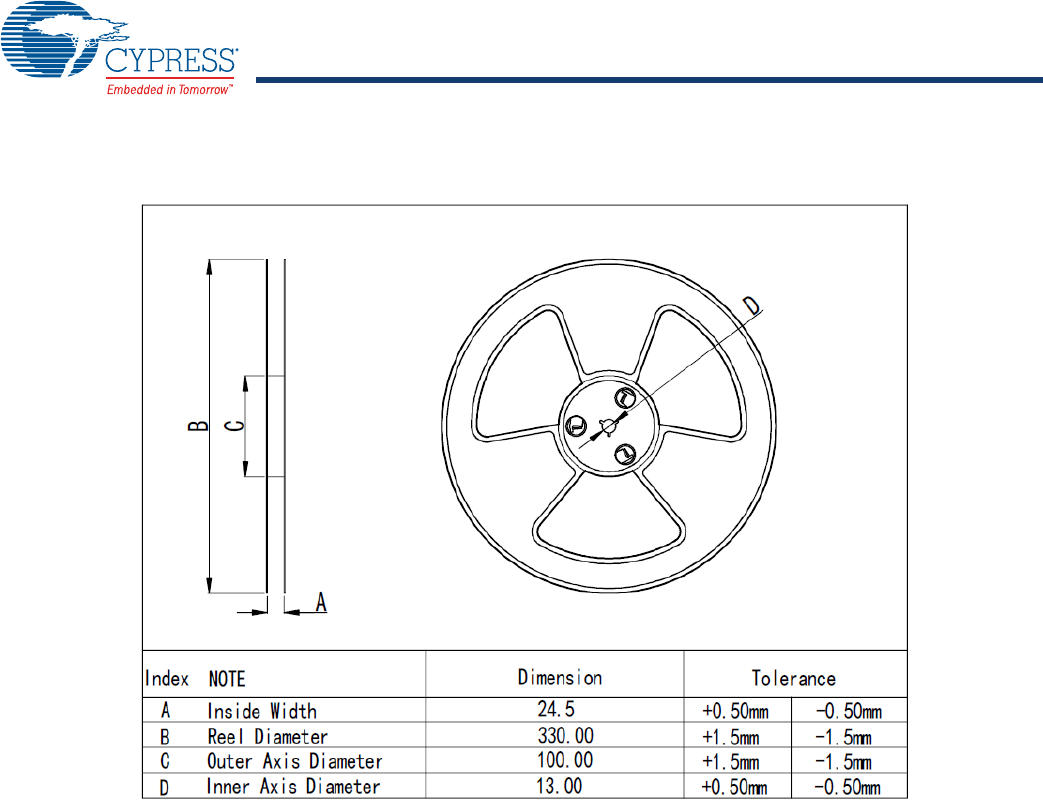
Figure 15 details reel dimensions used for the CYBT-013033-01.
Figure 15. Reel Dimensions
The CYBT-013033-01 is designed to be used with pick-and-place equipment in an SMT manufacturing environment. The
center-of-mass for the CYBT-013033-01 is detailed in Figure 16.
Figure 16. CYBT-013033-01 Center of Mass (TBD)
Document Number: 002-18414 Rev. ** Page 30 of 33
PRELIMINARY CYBT-013033-01
Ordering Information
Table 23 lists the CYBT-013033-01 part number and features. Table 24 lists the reel shipment quantities for the CYBT-013033-01.
The CYBT-013033-01 is offered in tape and reel packaging. The CYBT-013033-01 ships in a reel size of 1,500.
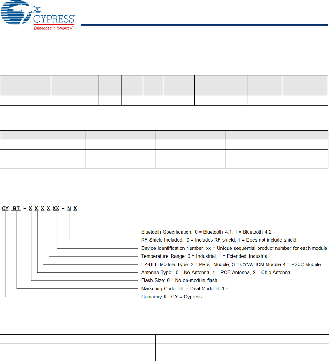
Part Numbering Convention
The part numbers are of the form CYBLE-ABCDEF-GH where the fields are defined as follows.
For additional information and a complete list of Cypress Semiconductor BLE products, contact your local Cypress sales
representative. To locate the nearest Cypress office, visit our website.
Table 23. Ordering Information
Part Number CPU
Speed
(MHz)
Flash
Size
(KB)
RAM
Size
(KB) UART BSC
(I2C) GPIO
Maximum
Apple MFi
Coprocessor
Interface Package Packaging
CYBT-013033-01 24 0 352 Yes Yes 2 Yes 13-SMT Tape and Reel
Table 24. Tape and Reel Package Quantity and Minimum Order Amount
Description Minimum Reel Quantity Maximum Reel Quantity Comments
Reel Quantity 1,500 1,500 Ships in 1,500 unit reel quantities.
Minimum Order Quantity (MOQ) 1,500 – –
Order Increment (OI) 1,500 – –
U.S. Cypress Headquarters Address 198 Champion Court, San Jose, CA 95134
U.S. Cypress Headquarter Contact Info (408) 943-2600
Cypress website address http://www.cypress.com
Document Number: 002-18414 Rev. ** Page 31 of 33
PRELIMINARY CYBT-013033-01
Acronyms Document Conventions
Units of Measure
Table 25. Acronyms Used in this Document
Acronym Description
BLE Bluetooth Low Energy
Bluetooth SIG Bluetooth Special Interest Group
CE European Conformity
CSA Canadian Standards Association
EMI electromagnetic interference
ESD electrostatic discharge
FCC Federal Communications Commission
GPIO general-purpose input/output
IC Industry Canada
IDE integrated design environment
KC Korea Certification
MIC Ministry of Internal Affairs and Communications
(Japan)
PCB printed circuit board
RX receive
QDID qualification design ID
SMT
surface-mount technology; a method for
producing electronic circuitry in which the
components are placed directly onto the surface
of PCBs
TCPWM timer, counter, pulse width modulator (PWM)
TUV Germany: Technischer Überwachungs-Verein
(Technical Inspection Association)
TX transmit
Table 26. Units of Measure
Symbol Unit of Measure
°C degree Celsius
kV kilovolt
mA milliamperes
mm millimeters
mV millivolt
A microamperes
m micrometers
MHz megahertz
GHz gigahertz
Vvolt

Document Number: 002-18414 Rev. ** Page 32 of 33
PRELIMINARY CYBT-013033-01
Document History Page
Document Title: CYBT-013033-01 EZ-BT™ Module
Document Number: 002-18414
Revision ECN Orig. of
Change Submission
Date Description of Change
** 5548256 DSO 01/27/2017 Preliminary datasheet for CYBT-013033-01 module.

Document Number: 002-18414 Rev. ** Revised January 27, 2017 Page 33 of 33
PRELIMINARY CYBT-013033-01
© Cypress Semiconductor Corporation, 2017. This document is the property of Cypress Semiconductor Corporation and its subsidiaries, including Spansion LLC ("Cypress"). This document, including
any software or firmware included or referenced in this document ("Software"), is owned by Cypress under the intellectual property laws and treaties of the United States and other countries worldwide.
Cypress reserves all rights under such laws and treaties and does not, except as specifically stated in this paragraph, grant any license under its patents, copyrights, trademarks, or other intellectual
property rights. If the Software is not accompanied by a license agreement and you do not otherwise have a written agreement with Cypress governing the use of the Software, then Cypress hereby
grants you a personal, non-exclusive, nontransferable license (without the right to sublicense) (1) under its copyright rights in the Software (a) for Software provided in source code form, to modify and
reproduce the Software solely for use with Cypress hardware products, only internally within your organization, and (b) to distribute the Software in binary code form externally to end users (either
directly or indirectly through resellers and distributors), solely for use on Cypress hardware product units, and (2) under those claims of Cypress's patents that are infringed by the Software (as provided
by Cypress, unmodified) to make, use, distribute, and import the Software solely for use with Cypress hardware products. Any other use, reproduction, modification, translation, or compilation of the
Software is prohibited.
TO THE EXTENT PERMITTED BY APPLICABLE LAW, CYPRESS MAKES NO WARRANTY OF ANY KIND, EXPRESS OR IMPLIED, WITH REGARD TO THIS DOCUMENT OR ANY SOFTWARE
OR ACCOMPANYING HARDWARE, INCLUDING, BUT NOT LIMITED TO, THE IMPLIED WARRANTIES OF MERCHANTABILITY AND FITNESS FOR A PARTICULAR PURPOSE. To the extent
permitted by applicable law, Cypress reserves the right to make changes to this document without further notice. Cypress does not assume any liability arising out of the application or use of any
product or circuit described in this document. Any information provided in this document, including any sample design information or programming code, is provided only for reference purposes. It is
the responsibility of the user of this document to properly design, program, and test the functionality and safety of any application made of this information and any resulting product. Cypress products
are not designed, intended, or authorized for use as critical components in systems designed or intended for the operation of weapons, weapons systems, nuclear installations, life-support devices or
systems, other medical devices or systems (including resuscitation equipment and surgical implants), pollution control or hazardous substances management, or other uses where the failure of the
device or system could cause personal injury, death, or property damage ("Unintended Uses"). A critical component is any component of a device or system whose failure to perform can be reasonably
expected to cause the failure of the device or system, or to affect its safety or effectiveness. Cypress is not liable, in whole or in part, and you shall and hereby do release Cypress from any claim,
damage, or other liability arising from or related to all Unintended Uses of Cypress products. You shall indemnify and hold Cypress harmless from and against all claims, costs, damages, and other
liabilities, including claims for personal injury or death, arising from or related to any Unintended Uses of Cypress products.
Cypress, the Cypress logo, Spansion, the Spansion logo, and combinations thereof, WICED, PSoC, CapSense, EZ-USB, F-RAM, and Traveo are trademarks or registered trademarks of Cypress in
the United States and other countries. For a more complete list of Cypress trademarks, visit cypress.com. Other names and brands may be claimed as property of their respective owners.
Sales, Solutions, and Legal Information
Worldwide Sales and Design Support
Cypress maintains a worldwide network of offices, solution centers, manufacturer’s representatives, and distributors. To find the office
closest to you, visit us at Cypress Locations.
Products
ARM® Cortex® Microcontrollers cypress.com/arm
Automotive cypress.com/automotive
Clocks & Buffers cypress.com/clocks
Interface cypress.com/interface
Internet of Things cypress.com/iot
Memory cypress.com/memory
Microcontrollers cypress.com/mcu
PSoC cypress.com/psoc
Power Management ICs cypress.com/pmic
Touch Sensing cypress.com/touch
USB Controllers cypress.com/usb
Wireless Connectivity cypress.com/wireless
PSoC® Solutions
PSoC 1 | PSoC 3 | PSoC 4 | PSoC 5LP
Cypress Developer Community
Forums | WICED IOT Forums | Projects | Video | Blogs |
Training | Components
Technical Support
cypress.com/support