DLP Design 000RF2 Short Range Transceiver User Manual DLP RF2 Data Sheet
DLP Design, Inc. Short Range Transceiver DLP RF2 Data Sheet
Users Manual Revision 2
Rev 1.0 (January 2005) DLP-RF2 DLP Design, Inc.
1
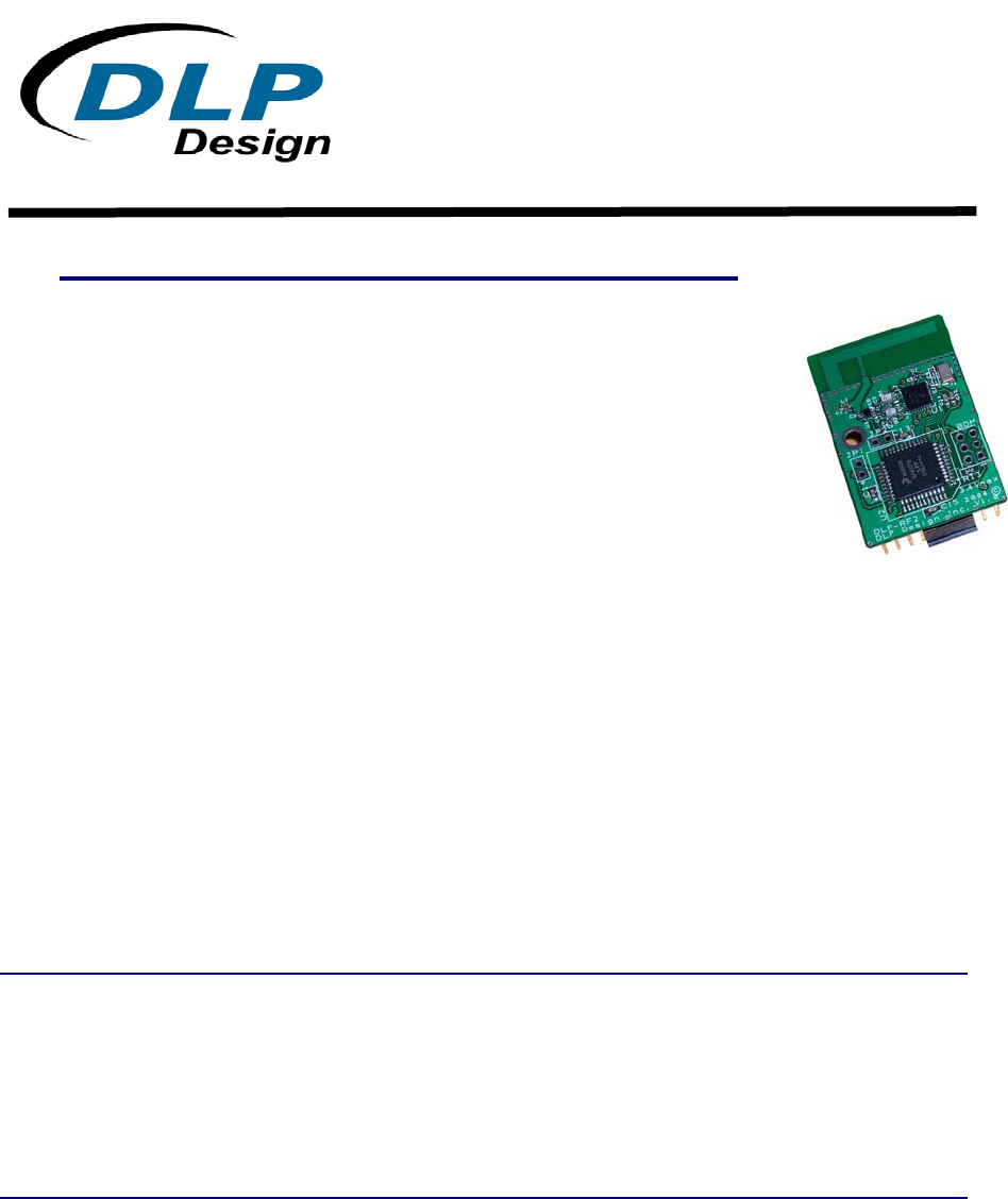
DLP-RF2
RF OEM Transceiver Module (Preliminary)
The DLP-RF2 combines a Freescale™ MC13192 2.4GHz Direct-
Sequence, Spread-Spectrum RF Transceiver IC and Freescale
MC9S08GT60 microcontroller to form an IEEE 802.15.4 compliant,
ZigBee™ ready, short-range transceiver module. The DLP-RF2 connects
to user electronics via a standard, 20-pin male header.
The MC9S08GT60 microcontroller is preprogrammed with DLP Design’s
Serial Interface Packet Processor (SIPP™ firmware) for accessing the
transceiver functions via simple serial calls. Interface to an external serial
host microcontroller/DSP/FPGA, etc. is accomplished via a simple 2-wire (RX, TX, and ground)
interface.
The SIPP firmware in the DLP-RF2 resides at the application layer and is based on Freescale’s
SMAC. The SIPP firmware provides basic access to DLP-RF2 functionality: Packet receive and
transmit, transceiver settings, EEPROM access, etc. The DLP-RF2 can also operate without a
serial host controller. Basic digital I/O, A/D conversions, temperature measurement, and
latching/non-latching relay control are available via the SIPP firmware.
The MC9S08GT60 can be reprogrammed (if desired) with user-supplied firmware via a 6-pin
BDM header that is compatible with the P&E USB-ML-12 and device programmers (purchased
separately).
Application Areas:
• Remote control and wire replacement in
industrial systems
• Wireless sensor networks
• Home automation and control
• Factory automation
• Heating and cooling systems
• Inventory management and RFID tagging
• Human interface devices
• Remote entertainment control • Wireless toys
Features:
• IEEE 802.15.4 Compliant & ZigBee ready
• Microcontroller pre-programmed with
• <35 microamp low-power mode
• Carrier-sense, multiple-access technology
SIPP firmware • Range: >700 feet, outdoor line of sight
Rev 1.0 (January 2005) DLP-RF2 DLP Design, Inc.
2
• Twelve I/O lines that can be configured for
digital input or output; seven lines can be
configured for analog input
• Agency approvals in place for immediate
deployment in the US, Canada, and
Europe
• Default reset via shorting two jumpers at
power-up
1.0 System Overview
Using the pre-programmed SIPP firmware, the DLP-RF2 can be used in conjunction with other
DLP-RF2 and/or DLP-RF1 modules to form simple point-to-point and star configuration
systems. Both the DLP-RF1 and the DLP-RF2 can serve as host/system controllers. In the
case of the DLP-RF1, the host is a user-supplied Windows, Linux, or Mac PC that is accessed
via a USB interface and user-supplied, 6-foot USB cable. In the case of the DLP-RF2, the host
is a user-supplied microcontroller/DSP/FPGA/etc. that is accessed via a 2-wire serial interface–
TX, RX, and ground. A host processor is not necessarily required by the DLP-RF2. The SIPP
firmware within the DLP-RF2 can be accessed remotely via another transceiver and can be
used to both gain access to the MC9S08GT60’s port pins for basic digital I/O and offer a few
hardware-specific functions for measuring system power supply voltage, measuring
temperature, and controlling relays. These functions require the presence of external hardware
(purchased separately).
Using the Z-Stack ZigBee Protocol Stack from Figure 8 Wireless (licensed separately), the
DLP-RF2 can be used in conjunction with other DLP-RF1/DLP-RF2 transceivers as well as
other MC13192-based ZigBee-ready devices to form complex point-to-point, star, and mesh
networks. (For more information on creating a ZigBee-enabled system, refer to Section 2.0 on
the topic of ZigBee.)
In a system using the preprogrammed SIPP firmware, each transceiver has a unique 16-bit ID
yielding a theoretical maximum of 65,535 transceivers. Every data packet handled by the SIPP
firmware must contain, at minimum, the number of bytes in the packet, the destination
transceiver ID (packet destination), the source transceiver ID (packet origin), and a command
byte.
As shipped from DLP Design, the DLP-RF2 has an ID of 2. If more than one DLP-RF2 is to be
used in a system, then this ID must be changed to a value higher than 2. Upon reset or power
up, the ID is read from non-volatile EEPROM memory. If JP1 is shorted at power up (or before
a reset), the default ID for the DLP-RF2 is set to 2 and other transceiver settings are also
returned to a default state in the EEPROM. (Refer to Section 3.2 for additional details.)
In addition to basic packet processing and port-pin manipulation, the SIPP firmware in the
DLP-RF2 offers a Low-Power Mode designed to conserve battery power. Holding PTC1
(Header Pin 16) low at power up enables the Low-Power Mode. Once enabled, the DLP-RF2 is
in Sleep Mode until awakened by activity on digital inputs that have been enabled to wake the
processor—or by a simple preset timeout. The setup parameters for this feature are also stored
in the non-volatile EEPROM memory. If PTC1 is not held low, then the microcontroller and RF
IC remain in full power mode, offering the fastest packet processing possible. (Refer to Section
3.2 for additional details.)

Rev 1.0 (January 2005) DLP-RF2 DLP Design, Inc.
3
2.0 ZigBee / Figure 8 Wireless
ZigBee™ is the only standards-based wireless networking technology for reliable, secure, cost-
effective, low-power monitoring and control solutions. ZigBee provides the network, security,
and application profile software layers for the IEEE 802.15.4 Global Wireless Standard. As a
leading member of the ZigBee Alliance with in-depth experience in mesh and wireless
communication protocols, Figure 8 Wireless provides a complete ZigBee software development
suite for application and product development.
ZigBee Primary Target Markets:
• Home Control
• Building Automation
• Industrial Automation
Figure 8 Wireless is a leader in making wireless device networking and the Extended Network a
reality. Figure 8's software products are the technological building blocks OEMs need to
produce standards-based ad hoc wireless device networks. Figure 8 Wireless has an
experienced wireless device networking team and strong partnerships with silicon radio
vendors, hardware providers, and system integrators. They are also a significant contributor to
the ZigBee Alliance, a non-profit organization defining global standards for reliable, cost-
effective, low power wireless applications.
**Contact Figure 8 Wireless for additional details on enabling the ZigBee protocol with the
DLP-RF1 and DLP-RF2 transceivers (www.figure8wireless.com; 858-552-8500).**
3.0 Preprogrammed Serial Interface Packet Processor (SIPP) Firmware
The C source code and flow diagrams for the SIPP firmware are available in a Developer’s Kit
as a separate purchase. The Developer’s Kit also contains the complete electrical schematics
for the DLP-RF2.
The source code for Freescale’s SMAC is available as a free download from
www.freescale.com.
A test program (DLP-RFTestAp.exe) is available as a free download from www.dlpdesign.com
that makes easy work of setting up the DLP-RF2 transceiver and testing its basic functionality.
Use of the DLP-RFTestAp.exe requires a serial interface (USB or RS232C, purchased
separately) between a host Windows PC and the DLP-RF2. Connection to the RF2 for the
purpose of setup and test can also be made via RF from another RF1 or RF2.
**Under this communication protocol, it is the responsibility of the serial host application
firmware to “Retry” transmissions that do not produce the anticipated reply.**
3.1 Packet Structure
Each SIPP firmware packet is comprised of 6 or more bytes. The following table outlines the
packet structure:

Rev 1.0 (January 2005) DLP-RF2 DLP Design, Inc.
4
PACKET STRUCTURE
Byte Description Comments
0
Number of bytes in the packet
following byte 0: 5-125
Each packet must contain (as a minimum) the
number of bytes, a destination ID, Source ID
and a command byte
1
Destination ID MSByte
ID Range: 1-65535*
ID:1 default for new DLP-RF1 transceivers
ID:2 default for new DLP-RF2 transceivers
ID:0 reserved for broadcast to all transceivers
2 Destination ID LSByte
3 Source ID MSByte
Range: 1-65535
4 Source ID LSByte
5 Command Byte
Command Range: 0xA0-0xDF
Both Command Packets and Reply Packets.
Every packet must have a command byte.
6 Data Byte(s) 0-120 bytes of data are allowed in the packet
*Note: Each transceiver in the system must have a unique ID. ID:0 is reserved for broadcast packets
sent by DLP-RF2 transceivers coming out of Sleep Mode.
3.2 Reserved EEPROM Locations
The EEPROM memory is a feature of the SIPP firmware and, as such, is only available if using
the DLP-RF2 with its firmware as shipped from DLP Design.
The EEPROM memory used by the SIPP firmware consists of a block of 32 bytes that reside
within the Flash program memory of the MC9S08GT60. The first 10 bytes (0-9) and the last
byte (31) are reserved for storing transceiver settings and checksum. Bytes 10 through 30 (user
area) are available for use by user’s host software.
Whenever the data in any EEPROM location is changed, the checksum location (EEPROM
Location 31) is automatically updated. At power up (or reset), if ever the calculated checksum
for the first 31 bytes does not match the value at EEPROM Location 31, the Default Reset
values for the transceiver settings are restored, and the checksum is recalculated and rewritten.
The values in the user area are preserved.
Additionally, if JP1 is shorted at power up (or reset), the default values for the transceiver
settings are restored, and the checksum is recalculated and rewritten. Again, values in the user
area are preserved.
The following table outlines the usage of the reserved EEPROM locations. These values are
read at power up, reset, or via SIPP firmware:

Rev 1.0 (January 2005) DLP-RF2 DLP Design, Inc.
5
EEPROM CONTENTS
Byte Description Options Default Reset
0 My ID MSB Range: 1-65,535 1 for RF1; 2 for RF2
1 My ID LSB 0 reserved for
broadcast commands
2 Transceiver Channel 0-15 (2.405GHz to 2.480GHz) 7 (2.440 GHz)
3 RF Transmit Power 0-15 (-16.6 to +3.5dBm into the baluns) 15 (+3.5dBm -Max
Power)
4
Sleep Time Length MSB
(DLP-RF2 Low-Power
Mode Only)
Range: 1-65,535; 5-second increments,
3.8 days max
For Example: 1=5 seconds, 12=1
minute, 120=10 minutes, 720=1 hour,
17,280=1day
5 seconds
5 Sleep Time Length LSB
6
Wake from Sleep, Host
Command Timeout after
Check-in (DLP-RF2 in
Low-Power Mode Only)
1-128 seconds
2 seconds
7
Baud Rate for RF2
Serial Host Controller
(DLP-RF2 Only)
0-2400; 1-4800; 2-9600; 3-14400;
4-19200; 5-38400; 6-128000;
7-250000
2 (9600 baud)
8 Port Pin Bit Field
(DLP-RF2 Only)
0x00-0xFF (A6B6B5B4 B3B2B1B0) 0x80; A6 monitored
9
DLP-RF2 Available
Features
(DLP-RF2 Only)
Bit 7 – Measures battery voltage
Bit 6 – Temperature sensor
Bit 5 – Relays
Bit 4 – Reserved
Bit 3 – Reserved
Bit 2 – Reserved
Bit 1 – Reserved
Bit 0 – Reserved
All bits cleared; no
features available
31 Checksum EX-OR of bytes 0-30 Calculated
3.3 Command Set
This Command Set is a feature of the SIPP firmware and, as such, is only available if using the
DLP-RF2 with its firmware as shipped from DLP Design.
Packets are broken down into two primary types: Command Packets and Reply Packets. The
host controller/PC originates all Command Packets. In the case of the DLP-RF2, the host is the
user-supplied serial host microcontroller/DSP/FPGA, etc.
If a Command Packet is received by the DLP-RF2 via the serial host interface with a destination
ID that matches the ID stored in the EEPROM of the DLP-RF2, then the MC9S08GT60 will
process the packet and reply to the serial host controller. If the ID in the packet does not match
the ID stored in EEPROM, then the packet is intended for a different destination and is
transmitted via the transceiver.

Rev 1.0 (January 2005) DLP-RF2 DLP Design, Inc.
6
If a packet is received via the RF transceiver with the correct ID, then the packet is either
processed by the MC9S08GT60 or forwarded on to the serial host. Commands between 0xA0
and 0xBF are Command Packets that are to be processed by the MC9S08GT60, while
commands between 0xC0 and 0xDF are Reply Packets and are forwarded on to the serial host.
If a packet arrives via the RF transceiver with an ID of 0 (zero), then the packet is a “broadcast”
packet intended for the system controller (the RF1/RF2 unit that is designated as system
controller). ID:0 packets are always immediately forwarded on to the host micro/PC.
If a packet arrives via the RF transceiver with an ID that does not match the EEPROM, then the
packet is ignored. The only exception to this is if “Return All Packets” Mode is enabled, in which
case the DLP-RF2 is monitoring packet traffic, and all unsolicited packets are returned to the
serial host.
** Under this communication protocol, it is the responsibility of the serial host application
firmware to “Retry” transmissions that do not produce the anticipated reply.**
Cmd
Packet Recipient
Description
# Bytes
Returned
Expected
Reply Cmd
0xA0 MC9S08GT60 Ping (no data) 0xC0
0xA1 MC9S08GT60 Set Transmit Power Level
1 Data Byte; Range: 0-15
0xC0
0xA2 MC9S08GT60 Set Transceiver Channel
1 Data Byte; Range: 0-15
0xC0
0xA3 MC9S08GT60 Reset Microcontroller (no data) 0xC0
0xA4 MC9S08GT60 Release immediately to Sleep
(DLP-RF2 only--no data)
0xC0
0xA5 MC9S08GT60 Measure energy on all channels (no data) 0xC3
0xA6 MC9S08GT60 Return all packets received to host
(Packet Watch Mode—no data)
0xC0
0xA7 MC9S08GT60 Return only packets with correct ID to host\
(Default--no data)
0xC0
0xA8 MC9S08GT60 Read EEPROM
1 Data Byte; Address: 0-31
0xC4
0xA9 MC9S08GT60 Write EEPROM and update checksum
2 Data Bytes; Address: 0-31; Data: 0-255
0xC5
0xAA MC9S08GT60 Read I/O pin, Port: 0xC6
0xAB MC9S08GT60 Set I/O pin direction, I/O Port: 0xC7
0xAC MC9S08GT60 Set/Clear I/O pin, Port: 0xC8
0xAD MC9S08GT60 Setup A/D, Mode: 0xC9
0xAE MC9S08GT60 Read A/D, Channel: 0xCA
0xAF MC9S08GT60 Reserved
0xB0 MC9S08GT60 Relay no-header packet to RF2 host - no
reply
0xCE
0xB1 MC9S08GT60 Relay no-header packet to RF2 host - wait
for reply with timeout
0xCE
0xB6 MC9S08GT60 Request Board Type (DLP-RF1, RF2)--
ROM and RFIC versions
0xCD

Rev 1.0 (January 2005) DLP-RF2 DLP Design, Inc.
7
0xB7 MC9S08GT60 Return Board ID (not available through RF
transceiver)
0xCF
0xB8 MC9S08GT60 Read VBAT (DLP-RF2 only; additional
hardware required)
0xCB
0xB9 MC9S08GT60 Read Temperature (DLP-RF2 only;
additional hardware required)
0xCC
0xC0 Serial / USB Generic Reply or “ACK” for all non-
broadcast commands
0xC1 Serial / USB Check-in from DLP-RF2 due to monitored
port pin input change
0xC2 Serial / USB Check-in from DLP-RF2 due to wake from
sleep
0xC3 Serial / USB Measured energy data
0xC4 Serial / USB EEPROM read reply
0xC5 Serial / USB Write EEPROM reply
0xC6 Serial / USB Read I/O pin reply
0xC7 Serial / USB Set direction reply
0xC8 Serial / USB Set/Clear I/O pin reply
0xC9 Serial / USB Setup A/D reply
0xCA Serial / USB Read A/D reply
0xCB Serial / USB Read VBAT reply
0xCC Serial / USB Read Temperature reply
0xCD Serial / USB Return board type--uC ROM and RF IC
versions
0xCE Serial / USB No-header packet reply
0xCF Serial / USB Return ID
Example: Below is a simple C program illustrating the Ping (0xA0) Command. This assumes
the presence of a transceiver with an ID of 1 issuing the Ping command and a second
transceiver with an ID of 0x13 (19 decimal) to receive and respond to the Ping command:
int m_DestID = 0x0013;
int m_SourceID = 0x0001;
unsigned char rx[126], tx[126];
int pos=1;//init packet index
tx[pos++] = (unsigned char)((m_DestID&0xff00)>>8); //Destination ID MSB
tx[pos++] = (unsigned char)(m_DestID&0x00ff); //Destination ID LSB
tx[pos++] = (unsigned char)((m_SourceID&0xff00)>>8); //Source ID MSB
tx[pos++] = (unsigned char)(m_SourceID&0x00ff); //Source ID LSB
tx[pos++] = 0xA0;//Command byte: Ping
tx[0] = pos-1;//assign number of bytes in packet to position zero
PutBuffer(tx, pos);//send tx out serial port
GetBuffer(rx, 6, TIMEOUTWAIT); //wait up to timeout for 6 bytes to return
if(rx[5] != 0xC0)//if Buffer Position 5 is not the expected reply (0XC0)
{
//No reply to the Ping command
//either retry the command or process the error
}

Rev 1.0 (January 2005) DLP-RF2 DLP Design, Inc.
8
4.0 Low-Power Mode (RF2 Only)
At power up, if MC9S08GT60 Port Pin PTC1 (Header Pin 16) is held low, the module will check
the initial state of selected port pins and immediately enter Low-Power Mode. This mode is a
feature of the SIPP firmware and is only available if using the DLP-RF2 with its firmware as
shipped from DLP Design. If pull-ups are enabled and the port pin is held low, then shutdown
current will be higher. Also, if the user electronics draw any current from port pins in Sleep
Mode, then the shutdown current will be higher. In this state, the MC13192 transceiver IC is in
Hibernate Mode, and the MC9S08GT60 is in Stop Mode. Total current draw for the DLP-RF2
module in this state is specified at less than 35 microamps at 3V.
The data byte stored at EEPROM Location 8 contains a bit field that is used to select which port
pins are to be watched for any change while in Low-Power or Idle Mode. For example, if a “1” is
set for Bit 7 at EEPROM Location 8, and if Port Pin PTA6 is set up as a digital input, and the
state of PTA6 changes (low to high, or high to low), then the MC9S08GT60 is brought out of
Low-Power Mode, and a packet is sent as a broadcast packet (Source ID=0) containing
Command 0xC1.
Bit Position: D7 D6 D5 D4 D3 D2 D1 D0 EEPROM [8]
Port Pin: A6 B6 B5 B4 B3 B2 B1 B0
The data bytes stored at EEPROM Locations 4 and 5 hold values that, when combined, are
used to set the length of time that the DLP-RF2 will remain asleep or in Low-Power Mode. The
range of time that the DLP-RF2 can be left asleep is from 5 seconds to 3.8 days. When this
amount of time has elapsed, the MC9S08GT60 is brought out of Low-Power Mode, and a
packet is sent as a broadcast packet (Destination ID=0) containing Command 0xC2.
The DLP-RF2 transmits a broadcast packet (Destination ID=0) for either wake from sleep or
change of a selected digital input. It is the user’s responsibility to establish a DLP-RF1 or DLP-
RF2 transceiver as a system controller to receive and process this packet. (Note that multiple
transceivers can be set up as system controllers as long as only one responds to a
wake-from-sleep packet from a specific DLP-RF2.) If the DLP-RF2 does not receive a reply to
this packet after a preset length of time, it will return to Sleep Mode to conserve battery power.
Command 0xA4 can be sent to the DLP-RF2 to instruct it to return to Sleep Mode immediately,
or the system controller can first request data from the DLP-RF2 before instructing it to return to
sleep.
The data byte stored at EEPROM Location 6 contains a value that determines how many half-
seconds a DLP-RF2 will remain awake waiting for a response from the system controller. If this
value is set to 1 (for example), then the DLP-RF2 will transmit its wake-from-sleep packet, wait
for 500 milliseconds for a reply, and retry one additional time before giving up and returning to
sleep.
Rev 1.0 (January 2005) DLP-RF2 DLP Design, Inc.
9
4.1 Reserved Mode
At power up, if MC9S08GT60 Port Pin PTE0 (Header Pin 17) is held low, the module will be set
up for operation in a dedicated usage mode. (Products currently under development by DLP
Design will utilize this mode.)
Note: Care must be taken to ensure PTE0 is not held low at power up (or reset) by user
electronics.
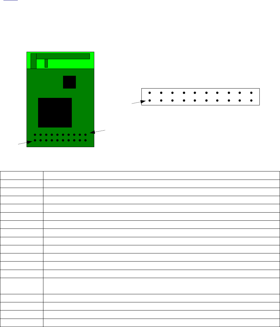
5.0 DLP-RF2 User Interface
GT 60
13192
Pin 1
Pin 20
Top View (Interface Header on bottom of PCB)
G
BBBBB
0
GG
NNN
DDD
T
G
K
B
X
D
1365
0
E
1
R
E
S
E
V
BA
4
R
26
BE
FC
RR
T0
XX
3/21
V
2//
C
X
CE
C
T
11
G
N
D
/
Pin 1
Pin # Header Pin Description
1 PTB1 (I/O) Port Pin B1 connected to the microcontroller; A/D Channel 1
2 PTB4 (I/O) Port Pin B4 connected to the microcontroller; A/D Channel 4
3 PTB3 (I/O) Port Pin B3 connected to the microcontroller; A/D Channel 3
4 Vref for A/D Converter (2.08V-VCC)
5 PTB6 (I/O) Port Pin B6 connected to the microcontroller; A/D Channel 6
6 PTB2 (I/O) Port Pin B2 connected to the microcontroller; A/D Channel 2
7 PTB5 (I/O) Port Pin B5 connected to the microcontroller; A/D Channel 5
8 PTA6 (I/O) Port Pin A6 connected to the microcontroller
9 PTB0 (I/O) Port Pin B0 connected to the microcontroller. A/D Channel 0
10,11,13,15 Ground
12 Power Supply--connect external power supply: 2.0 (MIN) to 3.4 Volts (MAX)
14 PTC0 (I/O) Port Pin C0 connected to the microcontroller; TxD2
16 PTC1 (I/O) Port Pin C1 connected to the microcontroller; low power enable
for SIPP firmware if held low at reset/power up
17 PTE0 (I/O) Port Pin E0 connected to the microcontroller; TxD1
18 PTE1 (I/O) Port Pin E1 connected to the microcontroller; RxD1
19 BKGD Background Debug
20 RESET# Microcontroller Reset Input

Rev 1.0 (January 2005) DLP-RF2 DLP Design, Inc.
10
6.0 Agency Identification Numbers
Agency compliance is a very important requirement for any product deployment. DLP Design
has obtained modular approval for its products so that the OEM only has to meet a few
requirements to be eligible for use under that approval. The corresponding agency identification
numbers are listed in the table below:
Part Number US/FCC CAN/IC
DLP RF2 SX9000RF2 5675A-000RF2
6.1 Integral Antenna
Important: The DLP-RF2 is approved for use with the integral antenna ONLY. Modifying the
DLP-RF2’s PCB antenna or modifying the PCB to use an external antenna will void all agency
compliance.
6.2 FCC/IC Requirements for Modular Approval
Any changes or modifications not expressly approved by DLP Design, Inc. could void the user’s
authority to operate the equipment.
6.3 Warnings Required in OEM Manuals
Warning: Operation is subject to the following two conditions: (2) This device may not cause
harmful interference, and (2) This device must accept any interference received, including
interference that may cause undesirable operation.
This device is intended only for OEM integrators under the following conditions:
1. The transmitter module may not be co-located with any other transmitter or antenna.
2. The module is approved using the FCC ‘unlicensed modular transmitter approval’
method.
As long as the two conditions are met, further transmitter testing will not be required. However,
the OEM integrator is still responsible for testing their end-product for any additional compliance
requirements required with this module installed (for example, digital device emissions, PC
peripheral requirements, etc.).
IMPORTANT NOTE: In the event that these conditions can not be met (for example certain co-
location with another transmitter, or a different antenna), then the FCC authorization is no longer
valid and the FCC ID may not be used on the final product. In these circumstances, the OEM
integrator will be responsible for re-evaluating the end product (including the transmitter) and
obtaining a separate FCC authorization.

Rev 1.0 (January 2005) DLP-RF2 DLP Design, Inc.
11
End Product Labeling
The final end product must be labeled in a visible area with the following: “Contains TX FCC ID:
SX9000RF2”.
RF Exposure Statements That May be Included in the Users Manual
The users manual for end users must include the following information in a prominent location
“IMPORTANT NOTE: To comply with FCC RF exposure compliance requirements, the antenna
used for this transmitter must not be co-located or operating in conjunction with any other
antenna or transmitter.”
Additional Information That Must be Provided to OEM Integrators
The end user should NOT be provided any instructions on how to remove or install the device.
8.0 Disclaimer
Neither the whole nor any part of the information contained herein nor the product described in
this datasheet may be adapted or reproduced in any material or electronic form without the prior
written consent of the copyright holder.
This product and its documentation are supplied on an as-is basis, and no warranty as to their
suitability for any particular purpose is either made or implied. DLP Design will not accept any
claim for damages whatsoever arising as a result of use or failure of this product. Your statutory
rights are not affected.
This product or any variant of it is not intended for use in any medical appliance, device, or
system in which the failure of the product might reasonably be expected to result in personal
injury.
This document provides preliminary information that may be subject to change without notice.
9.0 Contact Information
DLP Design, Inc.
1605 Roma Lane
Allen, TX 75013
Phone: 469-964-8027
Fax: 415-901-4859
Email: support@dlpdesign.com
Internet: http://www.dlpdesign.com