DMP ELECTRONICS AVL Auto Vehicle Locator (AVL) User Manual TechGuide AVL 1e3m7C
DMP ELECTRONICS INC. Auto Vehicle Locator (AVL) TechGuide AVL 1e3m7C
Contents
- 1. Users Manual Part I
- 2. Users Manual Part II
Users Manual Part II

22
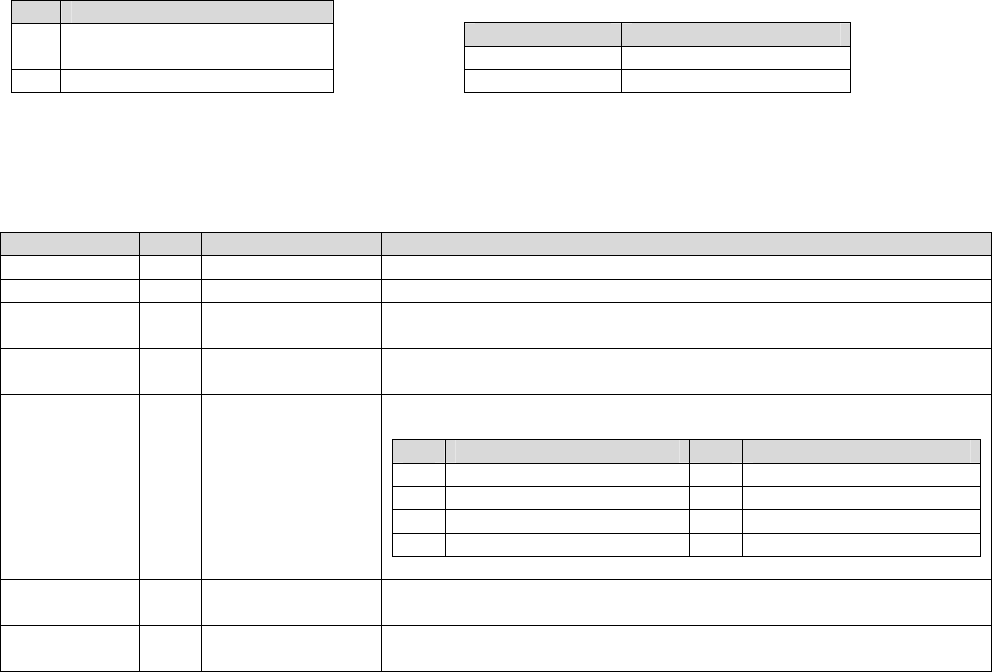
SRAM control port
I/O address 866H.
Bit Function
Bit0, 4 Change SRAM page 0~4
Bit6 Enable/disable SRAM write protect
Please refer our example codes to know how to setup and access GPIO.

23
Windows CE Example Codes
#include "stdafx.h"
unsigned char inp(int addr)
{
__asm
{
push edx
mov edx, DWORD PTR addr
in al, dx
and eax, 0xff
pop edx
}
}
void outp(int addr, unsigned char val)
{
__asm
{
push edx
mov edx, DWORD PTR addr
mov al, BYTE PTR val
out dx, al
pop edx
}
}
void main()
{
outp(0x2e, 0x87); /* unlock W83697UF configuration registers */
outp(0x2e, 0x87);
outp(0x2e, 0x2a); /* select GP2-5 device */
outp(0x2f, 0x00);
outp(0x2e, 0x2b); /* select GP80-83 device & enable COM3 */
outp(0x2f, 0x7c);
outp(0x2e, 0x2c); /* enable COM4 */
outp(0x2f, 0x55);
outp(0x2e, 0x07); /* select device 9, GP2-4 */
outp(0x2f, 0x09);
outp(0x2e, 0x30); /* active GP2-4 */
outp(0x2f, 0x07);
outp(0x2e, 0xf0); /* set GP2 as output mode */
outp(0x2f, 0x00);
outp(0x2e, 0xf3); /* set GP3 as input mode */
outp(0x2f, 0xff);
outp(0x2e, 0xf6); /* set GP4 as input mode */
outp(0x2f, 0xff);

24
outp(0x2e, 0x60); /* map to I/O address 610H */
outp(0x2f, 0x06);
outp(0x2e, 0x61);
outp(0x2f, 0x10);
outp(0x2e, 0x07); /* select device F, GP8 */
outp(0x2f, 0x0F);
outp(0x2e, 0x30); /* active GP8 */
outp(0x2f, 0x01);
outp(0x2e, 0xf0); /* set GP8 as output mode */
outp(0x2f, 0x00);
outp(0x2e, 0x60); /* map to I/O address 400H */
outp(0x2f, 0x04);
outp(0x2e, 0x61);
outp(0x2f, 0x00);
outp(0x2e, 0xaa); /* lock W83697UF configuration registers */
outp(0x2f, 0xaa);
/* After those code, programmer can access port 2/3/4/8 now */
/* output data to port 2 */
out(0x610, 0x55);
/* read data from port 3 */
inp(0x610)
/* read data from port 4 */
inp(0x611)
/* output data to port 8 */
out(0x610, 0xaa)
}
Technical Support
For more technical support, please visit http://www.dmp.tw/tech or mail to tech@dmp.tw
Using GPIO on AVL | 2006-04-25
End-of-Using GPIO on AVL

25
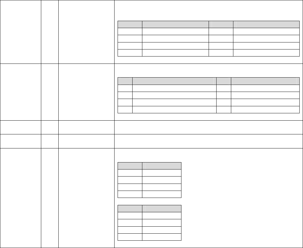
10.3. AVL Power Management Command Set
The power management of AVL is performed by a micro-p via I2C interface. The power management commands
are divided into two parts: setup and query commands. This document will show programmer those commands
and use our AVL library to do power management on AVL.
Setup Commands
Power ON setup command sequence is one command byte + one time data byte.
Power ON Condition Commands
Command Hex. Description
SET_OFF 81H Turn power off
SET_Ring 82H Wake on modem
SET_After 83H Power on after define time
SET_Every 84H Power on every define time
SET_GPI_ALL 8FH Wake on one of GPI pins
SET_GPI0 90H Wake on GPI0
SET_GPI1 91H Wake on GPI1
SET_GPI2 92H Wake on GPI2
SET_GPI3 93H Wake on GPI3
SET_Clear 85H Clear all trigger events. Time data will
be ignored
Time Data Byte
Bit Description
7 1: in hour
0: in minute
6-0 Time value in hour or minute.
Set all bits to 0 indicate right now.
Set all bits to 1 indicate disabled.

26
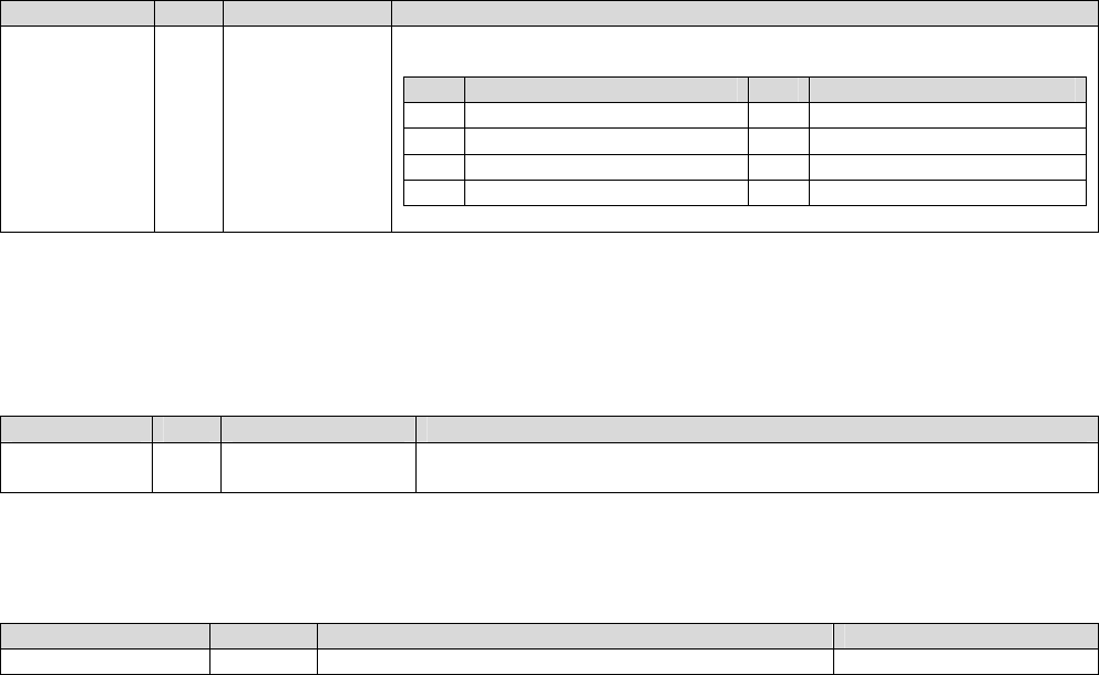
Command Hex. Description
SET_OFF 81H Turn power off
Example Command
Turn off power right now 81H + 00H
Turn off power after 10 minutes 81H + 0AH
Turn off power after 2 hours 81H + 82H
Disable turn off power setting 81H + FFH
Programmer can use 05H command to verify setting.
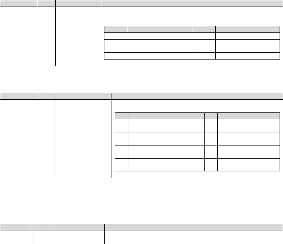
Command Hex. Description
SET_Ring 82H Wake on modem
Example Command
Wake on ring right now 82H + 00H
Wake on ring after 10 minutes 82H + 0AH
Wake on ring after 2 hours 82H + 82H
Disable Wake on ring 82H + FFH
Programmer can use 05H command to verify setting.
Command Hex. Description
SET_After 83H Power on after define time
Example Command
Wake on AVL right now 83H + 00H
Wake on AVL after 10 minutes 83H + 0AH
Wake on AVL after 2 hours 83H + 82H
Disable this command 83H + FFH
Programmer can use 05H command to verify setting.
Command Hex. Description
SET_Every 84H Power on every define time
Example Command
Wake on AVL right now 84H + 00H
Wake on AVL every 10 minutes 84H + 0AH
Wake on AVL every 2 hours 84H + 82H
Disable this command 84H + FFH
Programmer can use 05H command to verify setting.
Note: Before using SET_Ring command, please make sure that
GPRS is power on and supports wake on ring mode.

27
Command Hex. Description
SET_GPI_ALL 8FH Wake on one of GPI pins
Example Command
Turn on AVL power right now while one of GPIO is triggered 8FH + 00H
Disable this command 8FH + FFH
The valid time data bytes for this command are 00H and FFH.
Command Hex. Description
SET_GPI0 90H Wake on GPI0
Example Command
Turn on AVL power right now while GPI0 is triggered 90H + 00H
Disable this command 90H + FFH
The valid time data bytes for this command are 00H and FFH.
Command Hex. Description
SET_GPI1 91H Wake on GPI1
Example Command
Turn on AVL power right now while GPI1 is triggered 91H + 00H
Disable this command 91H + FFH
The valid time data bytes for this command are 00H and FFH.
Command Hex. Description
SET_GPI2 92H Wake on GPI2
Example Command
Turn on AVL power right now while GPI2 is triggered 92H + 00H
Disable this command 92H + FFH
The valid time data bytes for this command are 00H and FFH.
Command Hex. Description
SET_GPI3 93H Wake on GPI3
Example Command
Turn on AVL power right now while GPI3 is triggered 93H + 00H
Disable this command 93H + FFH
The valid time data bytes for this command are 00H and FFH.

28
Command Hex. Description
SET_Clear 85H Clear all trigger events. Time data will be ignored
Example Command
Clear all trigger events 93H + 00H
29
Query Commands
Power ON status query command is to send one query command and client will return one time date byte.
Time Data Byte
Bit Description
7 1: in hour
0: in minute
6-0 Time value in hour or minute.
“00H” indicates right now.
“FFH” is to disable time setting.
Voltage Data Bytes
The voltage is a 12-bit data.
Bit Description
Bit 7~0 of byte1 Bit 7~0 of voltage data.
Bit 3~0 of byte2 Bit 11~0 of voltage data.
Status Query Commands
Command Hex. Description Return
GET_OFF 01H Turn power off. Time data byte.
GET_Ring 02H Wake on modem. Time data byte.
GET_After 03H Power on after
define time.
Time data byte.
GET_Every 04H Power on every
define time.
Time data byte.
GET_EStatus 05H Query events
status.
For GET_EStatus query command, client will not return time data
byte. It will return all events status (0 is disabled and 1 is enabled):
Bit Description Bit Description
7 SET_OFF is enabled. 3 SET_GPI3 is enabled.
6 SET_Ring is enabled. 2 SET_GPI2 is enabled.
5 SET_After is enabled. 1 SET_GPI1 is enabled.
4 SET_Every is enabled. 0 SET_GPI0 is enabled.
GET_Voltage 40H Get current
voltage.
Return a 12-bits voltage data in 10mV unit. Ex: return 500H = 1280
-> 12.8V.
GET_OFF2 41H Get remainder
time to power off.
Time data byte.
30
GET_IStatus 42H Get input pins
status.
For GET_ISTatus query command, client will return a byte to indicate
status of input pins (0 is low and 1 is high):
Bit Description Bit Description
7 Reserved 3 GPI3
6 Reserved 2 GPI2
5 Reserved 1 GPI1
4 Ring 0 GPI0
GET_Trigger 43H Get the event to
trigger power on.
For GET_Trigger query command, client will return the event to
trigger power on:
Bit Description Bit Description
7 Input voltage event to trigger. 3 SET_GPI3 is triggered.
6 SET_Ring is triggered. 2 SET_GPI2 is triggered.
5 SET_After is triggered. 1 SET_GPI1 is triggered.
4 SET_Every is triggered. 0 SET_GPI0 is triggered.
GET_Diag 44H Return the second
byte.
It will be a second data byte after GET_Diag command. Return the
second byte to make sure it works properly.
Get_Version 45H Return PIC
version.
Return 1 in this version.
Get_VSwitch 47H Return voltage
detection switch.
Bit 1~0 of return byte indicate the switch status for power on voltage
detection. Default trigger voltage is:
Bit 1/0 Description
00 13.0V
01 13.3V
10 13.6V
11 13.9V
If input voltage > 18V, the trigger voltage is:
Bit 1/0 Description
00 26.0V
01 26.6V
10 27.2V
11 27.8V

31
Command Hex. Description Return
GET_OFF 01H Turn power off. Time data byte.
Example Send Command Read Response
Turn off power after 10 minutes 81H + 0AH
Query GET_OFF command setting 01H 0AH
Turn off power after 2 hours 81H + 82H
Query GET_OFF command setting 01H 82H
Command Hex. Description Return
GET_Ring 02H Wake on modem. Time data byte.
Example Send Command Read Response
Wake on ring after 10 minutes 82H + 0AH
Query GET_Ring command setting 02H 0AH
Wake on ring after 2 hours 82H + 82H
Query GET_Ring command setting 02H 82H
Command Hex. Description Return
GET_After 03H Power on after define time. Time data byte.
Example Send Command Read Response
Wake on AVL after 10 minutes 83H + 0AH
Query GET_Ring command setting 03H 0AH
Wake on AVL after 2 hours 83H + 82H
Query GET_Ring command setting 03H 82H
Command Hex. Description Return
GET_Every 04H Power on every define time. Time data byte.
Example Send Command Read Response
Wake on AVL every 10 minutes 84H + 0AH
Query GET_Ring command setting 04H 0AH
Wake on AVL every 2 hours 84H + 82H
Query GET_Ring command setting 04H 82H
32
Command Hex. Description Return
GET_EStatus 05H Query events
status.
For GET_EStatus query command, client will not return time data byte.
It will return all events status (0 is disabled and 1 is enabled):
Bit Description Bit Description
7 SET_OFF is enabled. 3 SET_GPI3 is enabled.
6 SET_Ring is enabled. 2 SET_GPI2 is enabled.
5 SET_After is enabled. 1 SET_GPI1 is enabled.
4 SET_Every is enabled. 0 SET_GPI0 is enabled.
Example Send Command Read Response
Wake on AVL every 10 minutes 84H + 0AH
Query event status 05H 10H
Wake on ring after 2 hours 82H + 82H
Query GET_Ring command setting 05H 50H
Command Hex. Description Return
GET_Voltage 40H Get current
voltage.
Return a 12-bits voltage data in 10mV unit. Real voltage (V) = (X *
1.221) / 1000 * 6 + 0.3.
Example Send Command Read Response
Query voltage of car 04H 05H + FEH
Real voltage = (5FEH * 1.221) / 1000 * 6 + 0.3 = 11.538084V
Command Hex. Description Return
GET_OFF2 41H Get remainder time to power off. Time data byte.
Example Send Command Read Response
Turn off power after 10 minutes 81H + 0AH
Get remainder time to power off 41H 0AH
Turn off power after 2 hours 81H + 82H
Get remainder time to power off 41H 82H
33
Command Hex. Description Return
GET_IStatus 42H Get input pins
status.
For GET_ISTatus query command, client will return a byte to indicate
status of input pins (0 is low and 1 is high):
Bit Description Bit Description
7 Reserved 3 GPI3
6 Reserved 2 GPI2
5 Reserved 1 GPI1
4 Ring 0 GPI0
Example Send Command Read Response
Get input status 41H 02H (GPI1 is high, other pins are low)
Command Hex. Description Return
GET_Trigger 43H Get the event to
trigger power on.
For GET_Trigger query command, client will return the event to
trigger power on:
Bit Description Bit Description
7 Input voltage event to
trigger.
3 SET_GPI3 is
triggered.
6 SET_Ring is triggered. 2 SET_GPI2 is
triggered.
5 SET_After is triggered. 1 SET_GPI1 is
triggered.
4 SET_Every is triggered. 0 SET_GPI0 is
triggered.
Example Send Command Read Response
Wake on AVL every 10 minutes 84H + 0AH
Turn off power right now 81H + 00H
AVL will wake on after 10 minutes
Get the event to trigger power on 43H 10H
Command Hex. Description Return
GET_Diag 44H Return the second
byte.
It will be a second data byte after GET_Diag command. Return the
second byte to make sure it works properly.
Example Send Command Read Response
Run diagnostic 44H + 55H 55H
Run diagnostic 44H + AAH AAH
34
Command Hex. Description Return
Get_Version 45H Return PIC version. Return 1 in this version.
Example Send Command Read Response
Get firmware version 45H 01H
Command Hex. Description Return
Get_VSwitch 47H Return voltage
detection switch.
Bit 1~0 of return byte indicate the switch status for power on
voltage detection. Default trigger voltage is:
Bit 1/0 Description
00 13.0V
01 13.3V
10 13.6V
11 13.9V
If input voltage > 18V, the trigger voltage is:
Bit 1/0 Description
00 26.0V
01 26.6V
10 27.2V
11 27.8V
Example Send Command Read Response
Get DIP switch status 47H 01H (switch 1 is on and switch 0 is off)
AVL Power Management Command Set | 2006-04-11
End-of-AVL Power Management Command Set

35
10.4. AVL Power Management Programming Reference
The power management functions on AVL is handled by a PIC via I2C interface. This document will show
programmers our demo codes.
Here is the definition on AVL Windows CE example code according power management commands:
#define AVL_POWER_WAKE_ON_RING 0 // wake on ring
#define AVL_POWER_WAKE_ON_1_TIME 1 // power on after define time
#define AVL_POWER_WAKE_ON_EVERY_TIME 2 // power on every define time
#define AVL_POWER_WAKE_ON_ALL_GPI 3 // wake on one of GPI pins
#define AVL_POWER_WAKE_ON_GP_0 4 // wake on when gp0 is trigged
#define AVL_POWER_WAKE_ON_GP_1 5 // wake on when gp1 is trigged
#define AVL_POWER_WAKE_ON_GP_2 6 // wake on when gp2 is trigged
#define AVL_POWER_WAKE_ON_GP_3 7 // wake on when gp3 is trigged
Before using AVL power management functions, programmer has to enable I2C interface. Call
AVL_POWER_init():
bool AVL_POWER_init();
// init AVL power module, you have to run this function first
// return false if init fail
To disable I2C interface and power management function, call AVL_POWER_close():
void AVL_POWER_close();
// close power library
char *AVL_POWER_version();
// return the AVL POWER Library version string
char *AVL_POWER_build_date();
// return the AVL POWER Library build date.
bool AVL_POWER_get_pic_version(BYTE &val);
// get the Power module PIC version
// !! return false if pic is busy for execute command !!
bool AVL_POWER_power_off(int h_m, int t);
// set power off command,
// !! this function will return false when any argument error !!
// !! and do not execute command. !!
// !! return false if pic is busy for execute command !!
// h_m : means the t field in hour or minutes type, 0 for minutes, others for hour
// t : how many hours(or minutes) to power off, 0 = power off right now
// : value from 0 ~ 126
bool AVL_POWER_clear_power_off();
// diable the power off command,
// after you issuse the power off command, you can use this function
// to cancel it.
To perform wake on AVL by trigger event, programmer can use this function:
bool AVL_POWER_wake_on_event(int event_type, int h_m, int t)
// !! this function will return false when any argument error !!

36
// !! and do not execute command. !!
// !! return false if pic is busy for execute command !!
// event_type : power on event type, defined in AVL_POWER_WAKE_ON_*
// h_m : means the t field in hour or minutes type, 0 for minutes, others for hour
// t : how many hours(or minutes) to power on, 0 = power on when event trigged
// : other values means delay [t] hours(or minutes) then power on.
// : value from 0 ~ 126
bool AVL_POWER_disable_wake_on_event(int event_type);
// clear the power on event
// !! this function will return false when any argument error !!
// !! and do not execute command. !!
// !! return false if pic is busy for execute command !!
// event_type : power on event type, defined in AVL_POWER_WAKE_ON_*
bool AVL_POWER_clear_all_wake_on_event();
// clear all power on event
// !! return false if pic is busy for execute command !!
bool AVL_POWER_get_power_off_timer(int &h_m, int &t);
// get power off timer setted before
// !! return false if pic is busy for execute command !!
// h_m : means the t field in hour or minutes type, 0 for minutes, others for hour
// t : how many hours(or minutes) to power on, 0 = power on when event trigged
// : other values means delay [t] hours(or minutes) then power on.
// : value from 0 ~ 126
bool AVL_POWER_get_wake_on_timer(int event_type, int &h_m, int &t);
// get event wake on timer setted before
// !! this function will return false when any argument error !!
// !! and do not execute command. !!
// !! return false if pic is busy for execute command !!
// event_type : power on event type, defined in AVL_POWER_WAKE_ON_*
// h_m : means the t field in hour or minutes type, 0 for minutes, others for hour
// t : how many hours(or minutes) to power on, 0 = power on when event trigged
// : other values means delay [t] hours(or minutes) then power on.
// : value from 0 ~ 126
bool AVL_POWER_get_event_status(AVL_POWER_Event_Status *event_status);
// get event status,
// !! return false if pic is busy for execute command !!
// see struct AVL_POWER_Event_Status for more information
bool AVL_POWER_get_input_status(AVL_POWER_Input_Status *input_status);
// get input status,
// see struct AVL_POWER_Input_Status for more information
bool AVL_POWER_get_power_on_type(AVL_POWER_Power_On_Event_Type *power_on_type);
// get power up event type
// see struct AVL_POWER_Power_On_Event_Type for more information

37
bool AVL_POWER_get_current_voltage(float &val);
// get current voltage data
// !! return false if pic is busy for execute command !!
bool AVL_POWER_get_remainder_time_to_power_off(int &h_m, int &t);
// get remainder time to power off
// !! return false if pic is busy for execute command !!
// h_m : means the t field in hour or minutes type, 0 for minutes, others for hour
// t : how many hours(or minutes) to power on, 0 = power on when event trigged
// : other values means delay [t] hours(or minutes) then power on.
// : value from 0 ~ 126
bool AVL_POWER_get_sw_setting(BYTE &val);
// get the DIP SWITCH SETTING
// !! return false if pic is busy for execute command !!
Examples
AVL_POWER_init();
// power off AVL right now
AVL_POWER_power_off(0, 0);
// power off AVL after 10 minutes
AVL_POWER_power_off(0, 10);
// power off AVL after 1 hour
AVL_POWER_power_off(1, 1);
// wake on ring
AVL_POWER_wake_on_event(AVL_POWER_WAKE_ON_RING, 0, 0);
// disable wake on ring
AVL_POWER_disable_wake_on_event(AVL_POWER_WAKE_ON_RING);
AVL_POWER_close();
Technical Support
For more technical support, please visit http://www.dmp.tw/tech or mail to tech@dmp.tw
AVL Power Management Programming Reference | 2006-04-25
End-of-AVL Power Management Programming Reference

38
Chapter 11
11. AVL COMMUNICATION BOARDS
DMP offers two different models of AVL75 computer system namely: (1)the AVL Basic system and
(2)AVL Basic+OBD-II system. The AVL75 Basic system comes with 128MB System memory + 32MB
DOM. Depending on the memory capacity requirement of your development in AP software + O/S,
the IDE flash memory (DOM) can be upgraded to 64MB, 128MB, 256MB and 512MB. The AVL Basic
system consists of an x86 CPU board with the GPS & GPRS function. AVL75 was designed with the
intention to provide the AVL software developers the proper hardware platform and tool in creating
the required application software for its vehicle tracking market.
The AVL75 was designed using the modular concept in providing the BASIC unit system and the
OPTION add-on modules. Listed below is the summary of AVL75 different modules and part
numbers:
AVL module no. Device Function description
AVL-1 GPS Tracking and Positioning
AVL-2 & AVL-3 GPRS Data Transmission &
Communication
AVL-5 OBD-II Car networking and control
Hereafter, we are delighted to share the subassembly of the add-on modules with it’s corresponding
interface cards. Please refer to the section of your desired assembly instruction or removal
procedure.
Operational Procedure
11.1. Uncovering your AVL75
11.2. Removing your GPRS Modem card
11.2.1. Adding the GPRS add-on Modem card
11.3. Removing your OBD-II module
11.3.1. Adding the OBD-II card
39
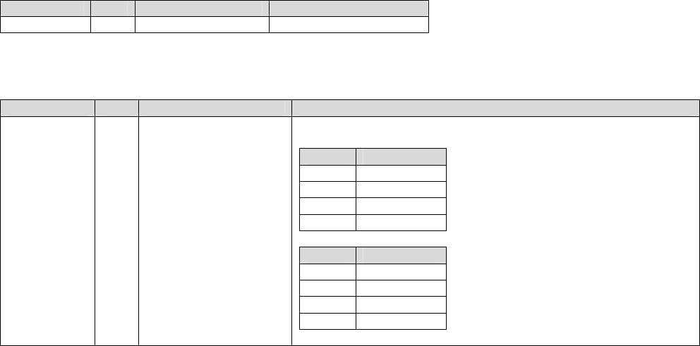
11.1 Uncovering your AVL75
Software developers may open your AVL75 to check the necessary hardware components for its
needed application. Below please find the disassembly operation.
1. Prepare the following tools & things:
Philips type (+) and Slotted type
screwdrivers.
Long nose tweezers.
A small papercup (to put your screws and
nuts).
Two clean towels for cushion (you may
use an anti-static bubble plastic bag too).
2. Separate and put the 2 clean towels
(cushion) on the flat surface of your working
desk.
3. Then put your AVL750MWB computer system
on one cushion.
4. The AVL75 system is made up of 2-C shape
chassis, top cover and base chassis are
adjacent to each other.
5. Prepare to unlock the 8 screws of your AVL75
system: 4 screws are behind the top cover,
and 2 each at the front panel and rear
backplane All screws are Philips (+) type.
6. Take your Philips screwdriver to unlock the 4
screws behind the top cover of your AVL75
system.
7. Then unlock the 2 screws on the front panel.
40
8. And then unlock the remaining 2 screws at
the rear backplane.
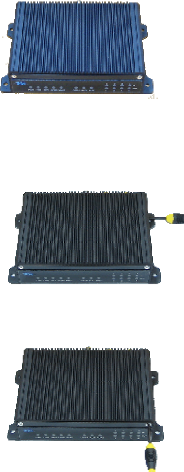
9. Rotate your AVL75 system in a 180-degrees
direction (rear panel facing you). Hold your
AVL 75 system with both hands, your thumbs
atop the systems and four fingers beneath
the device.
10. Uphold your AVL75 system away, one feet
(30 cm) from the working desk, depress the
top cover with both thumbs, until the top
cover comes off the base chassis as seen in
the next photo.
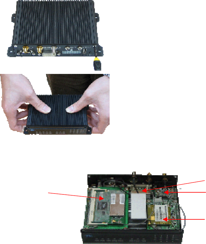
GPS card
WIFI LAN card AVL-5: OBD-II card
VIA VT6656 Wireless LAN
(on AVL-4 module)
GPRS Modem card
Siemens MC55 GPRS
(on AVL-2 module)
41
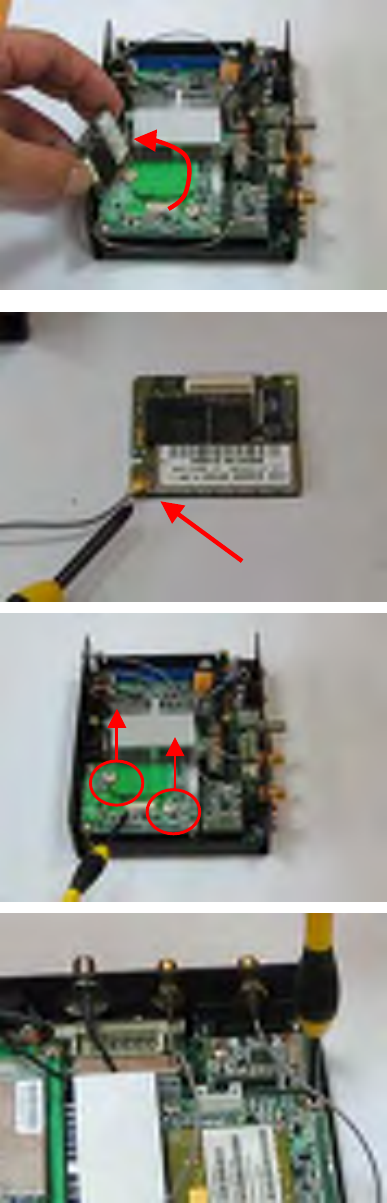
11.2 Removing your GPRS Modem card
1. Using a long nose tweezers or a hex cone
driver, unlock and remove the 2 nuts from
the Siemens MC55 Modem card (as seen on
the left photo).
2. The 2 nuts are located diagonally on the
edges of the MC55 modem card. Unlock the
first nut.
3. Unlock the second nut of the MC55 modem
card.
4. Rotate your AVL75 system 90-degrees
clockwise. Hold the diagonal edges of your
MC55 modem card with one hand, and slowly
jiggle the card until it is free from the bottom
connector.
42
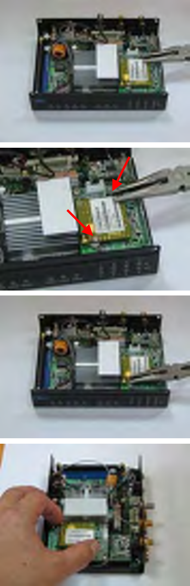
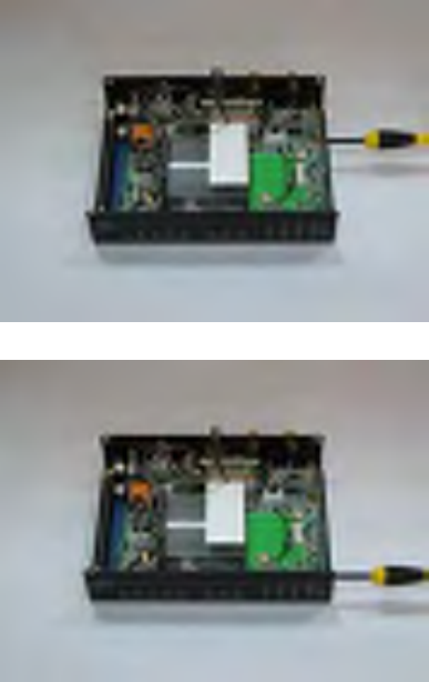
5. Turn over the MC55 modem card to look for
the antenna connection.
6. Remove the antenna connection by pulling
the clip pin upwards from it’s socket on the
MC55 modem card.
7. After releasing the MC55 modem card from
AVL-2 module, now remove two each of a
plastic and paper spacers from the AVL-2
module.
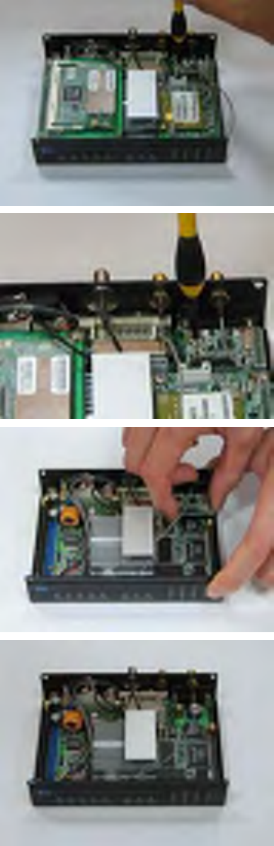
8. Turn the AVL75 unit in a 90-degrees counter
clockwise. Start removing the four screws of
AVL-2 module with a Philips screw driver.
43
9. The connector is located at the right side of
your AVL-1 main board. Slightly lifting one
edge of the right side of your AVL-2 module
with a slotted (-) screwdriver. Avoid
damaging the connector and socket, do not
use force intrusion.
10. Then do the same by slightly lifting the
opposite edge of the connector of your
AVL-2 module with a slotted screwdriver.
11. Then slowly jiggle (shake) the AVL-2
module until it is free from the bottom
socket.
11.2.1. Adding the GPRS add-on Modem card
1. To install the GPRS modem card, do the reverse procedure.
2. Locate J16 of your AVL-1 main board in your AVL75 system, and plug on the AVL-2 daughter
board. Note: J16 (AVL-1) is a 22x2 pin - 2.0mm pitch box connector.
3. Secure the 4 screws on the edges of the AVL MC55/56 GPRS modem add-on module (AVL-2).
4. Install the MC55 modem card onto AVL-2, you may contact DMP or our nearest sales office to
purchase the add-on module & MC55/56 modem card.
44
11.3 Removing your OBD-II module
1. Locate and unlock one screw of your AVL-5
with a Philips screwdriver.
2. Viewing the photo on the left side, there is
only one screw used for locking the OBD-II
card (AVL-5).
3. Hold the edges and then slowly jiggle (and
shake) the OBD-II card until it is free from
the bottom connector.
4. Now you have remove all three option cards
(WIFI card, MC55 GPRS card & AVL-5) and
its’ corresponding two expansion cards
(AVL-2 & AVL-3).
45
11.3.1. Adding the OBD2 card
1. To install the OBD-II card, do the reverse procedure.
2. Locate J10 of your AVL-1 main board in your AVL75 system, and plug on the AVL-5 daughter
board. Note: J10 (AVL-1) is a 10x2 pin - 2.0mm pitch box connector.
3. To install OBD-II card, secure one screw on top of the OBD-II card (AVL-5) to AVL-1 main
board..
4. You may contact DMP nearest sales office to purchase the OBD-II card.
<End>
46
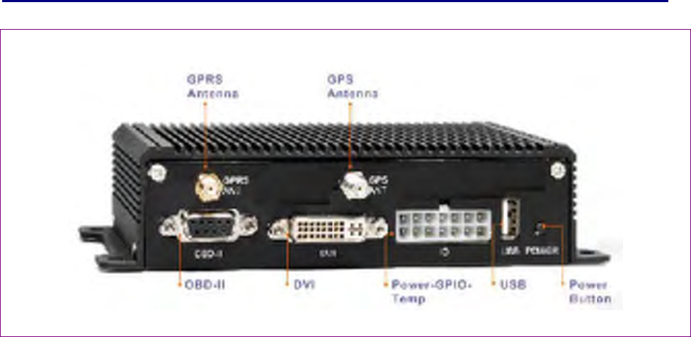
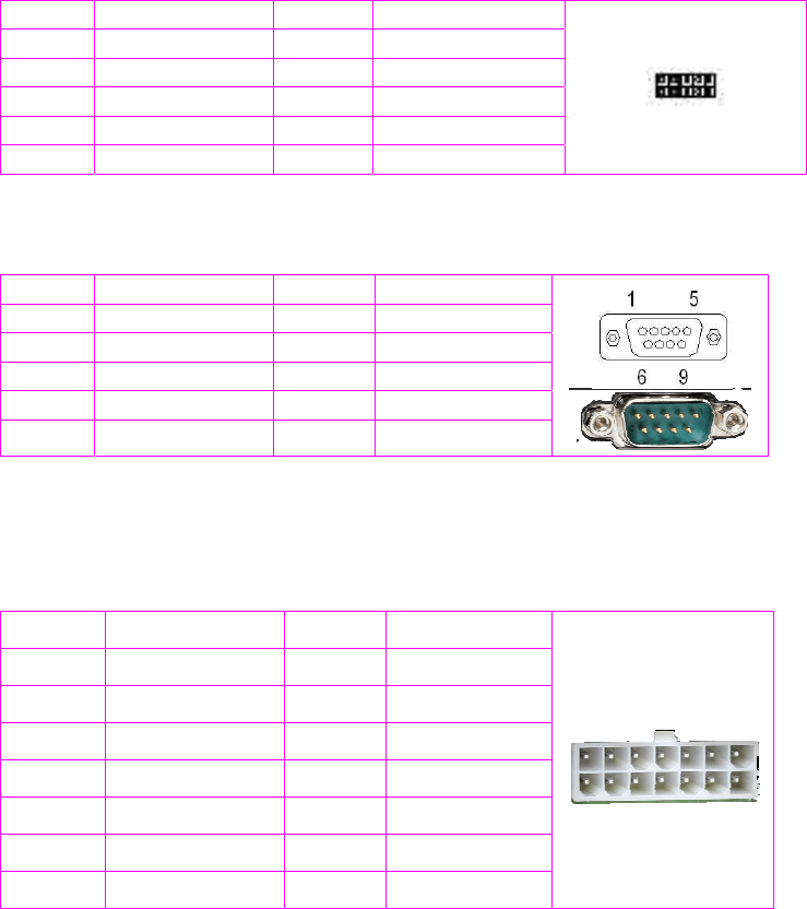
APPENDIX A: REAR CONNECTOR PIN ASSIGNMENT SUMMARY
Herewith is the visible Rear Connector, this is the version with DVI connector.
FIGURE A1 : AVL75 Back panel / OBD2+DVI
Looking at the above figure A1, starting from the top-to-bottom and left-to-right. You can
find the pin assignment of each connector.
47
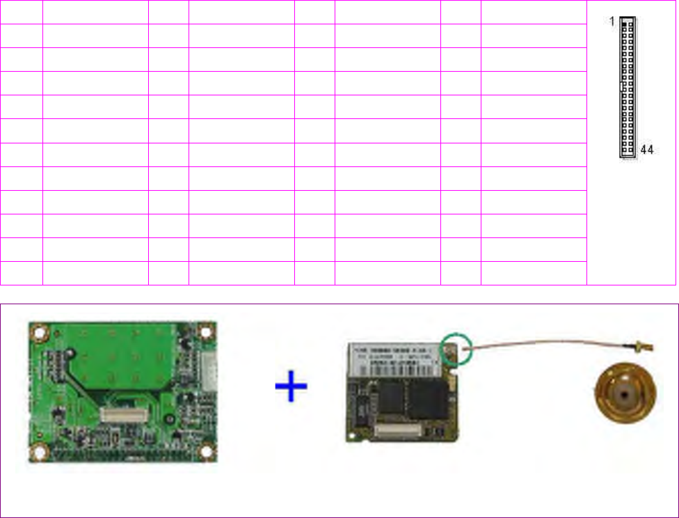
GPRS ANT
AVL-2 / Modem Interface Module (Daughter Board)
J1 (DM39) /22x2 pin –2.0mm ∅ Pin header connector (male)
J16 (DM38) : COM4 /22x2 pin –2.0mm ∅ Pin header connector (male)
PIN#
Signal Name PIN#
Signal Name PIN#
Signal Name PIN#
Signal Name
1 DCD4\ 12 GND 23 PORT35 34 SIM-RST
2 RXD4\ 13 VSUS4V 24 PORT25 35 SIM-GND
3 TXD4\ 14 VSUS4V 25 PORT36 36 SIM-CLK
4 DTR4\ 15 NC (USB2-) 26 NC (PORT26) 37 GND
5 GND 16 NC (USB+) 27 PORT37 38 GND
6 DSR4\ 17 RING\ 28 NC (PORT27) 39 LINL
7 RTS4\ 18 VXX 29 GND 40 LOUTL1
8 CTS4\ 19 MODEM-LED 30 GND 41 GND
9 RI4\ 20 NC (PCIRST-) 31 NC (SIM-VPP) 42 GND
10 VCC 21 PORT34 32 SIM-VCC 43 LINR
11 GND 22 PORT24 33 SIM-IO 44 LOUTR1
FIGURE A2 : AVL-2 / Modem Interface
Module FIGURE A3 : MC55 GPRS Modem Card
(GPRS ANT connector : SMA female)
48
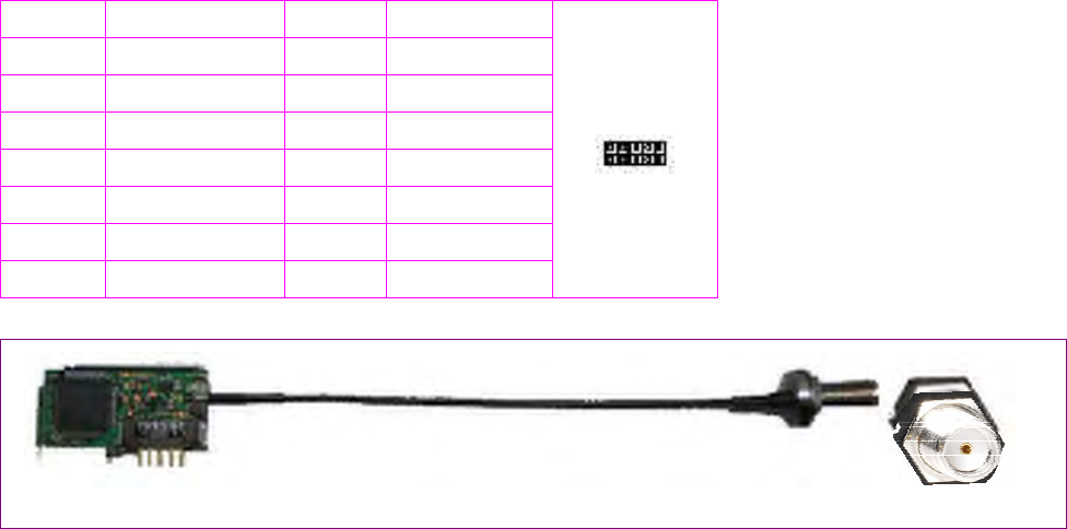
GPS ANT
J9 (DM38): COM3 / GN-80-V GPS / GN-80-V Connector (INTERNAL)
PIN# Signal Name PIN# Signal Name
1 NC 2 GND
3 RXD3 4 TXD3
5 1PPS 6 PCIRST-
7 VXX 8 GND
9 VCC3 10 VCC
11 G1 (GND) 12 G2 (GND)
13 G3 (GND) 14 --
GPS ANT connector: SMA female
FIGURE A6 : FURUNO GPS card
49
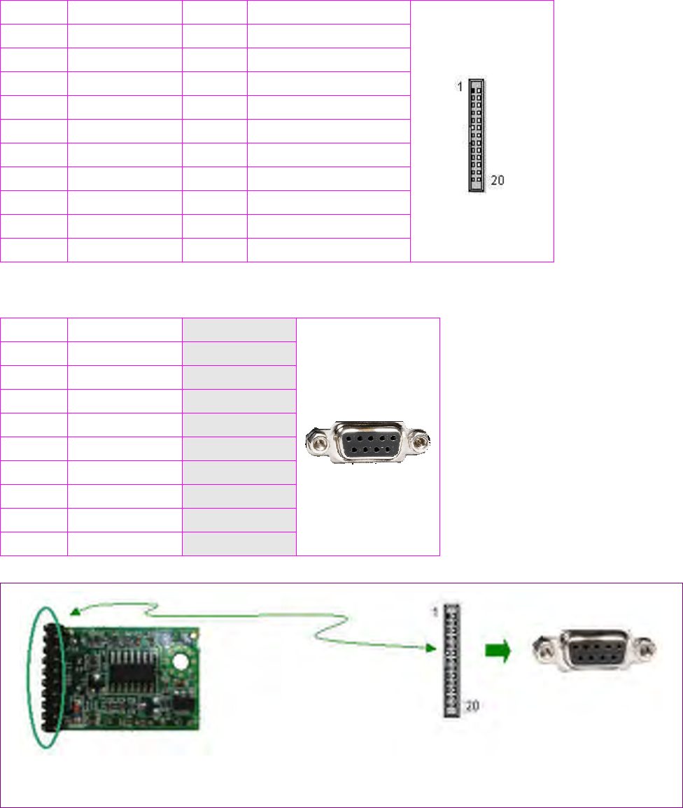
OBD-II & COM2
AVL-1 / Selectable On-board diagnostic & Serial port (COM2)
J10 (DM38): OBD-II & COM2 signals / 10x2 pin - 2.0mm ∅ Pin header connector (male)
PIN# Signal Name PIN# Signal Name
1 TXD2 2 PORT54
3 RXD2 4 PORT55
5 PCIRST- 6 PORT56
7 OBD-LED 8 PORT57
9 GND 10 GND
11 ISO9141/K 12 ISO9141/L
13 J1850/VPWN+
14 J1850/PWM-
15 CAN+ 16 CAN-
17 GND 18 GND
19 OBD-PWR 20 OBD-PWR
AVL-1 / On-board diagnostic
J12 (DM38): OBD-II (Option 1) / 9-pin Dsub Connector
PIN# Signal Name
Signal Name
1 GND DCD2
2 GND RXD2
3 CAN+ TXD2
4 ISO9141/K DTR2
5 CAN- GND
6 J1850/VPWN- DSR2
7 J1850/VPWN+
RST2
8 ISO9141/L CTS2
9 OBD-PWR RI2
J12 (DM38) : OBD-II (Option 1) / 9-pin D-Sub connector
FIGURE A7 : OBD-II Card
OBD-II connects to 9-pin D-Sub via 20-pin box header
50
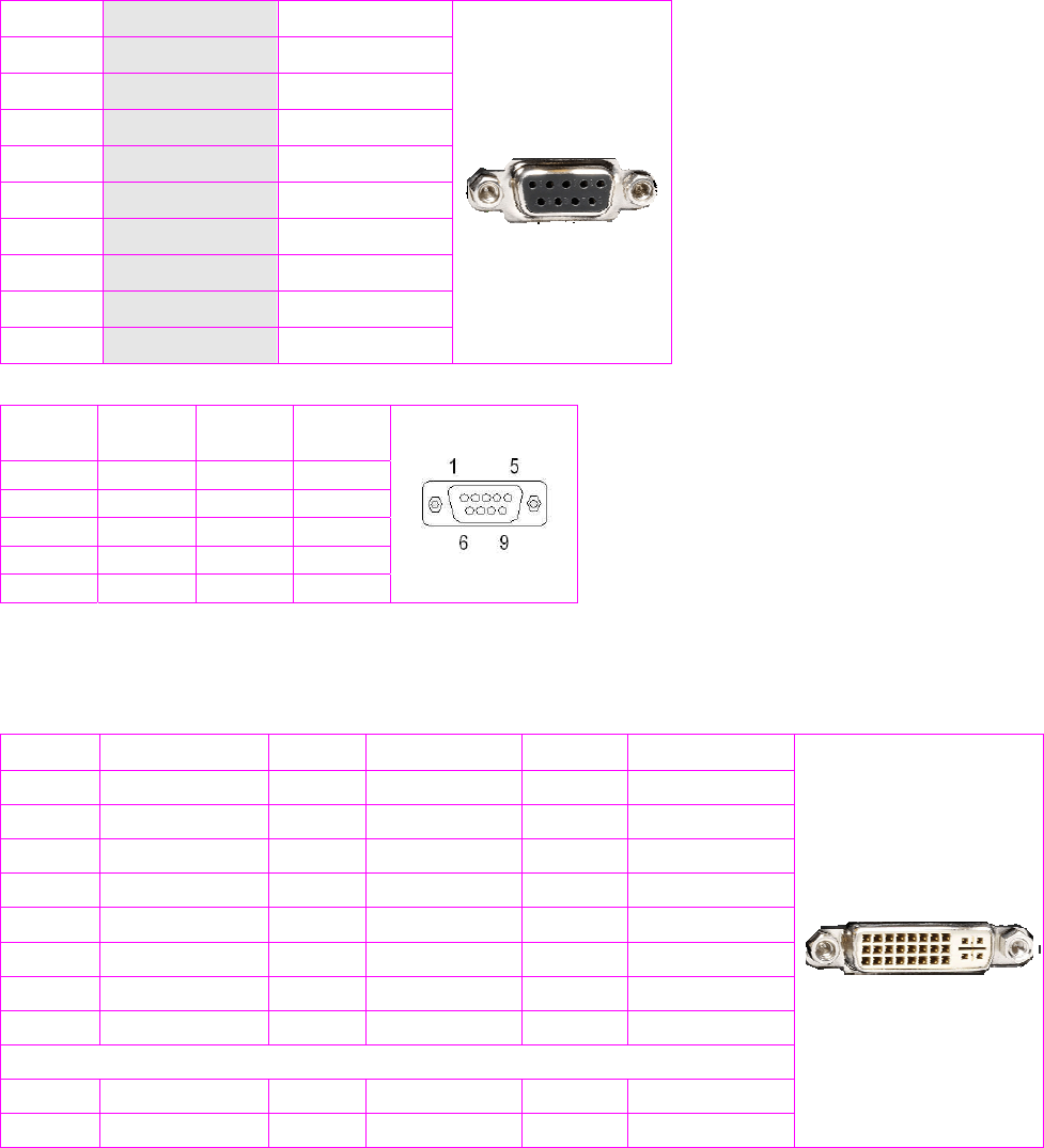
AVL-1 / RS232 Serial port
J10 (DM38): COM2 (Option 2) / 9-pin Dsub Connector
PIN# Signal Name Signal Name
1 GND DCD2
2 GND RXD2
3 CAN+ TXD2
4 ISO9141/K DTR2
5 CAN- GND
6 J1850/VPWN- DSR2
7 J1850/VPWN+
RST2
8 ISO9141/L CTS2
9 OBD-PWR RI2
J11 (DM38) : COM2 / Serial port (Option 2) / 9-pin D-Sub connector
Pin # Signal
Name Pin # Signal
Name
1 DCD1 2 RXD1
3 TXD1 4 DTR1
5 GND 6 DSR1
7 RTS1 8 CTS1
9 RI1 -- --
DVI & VGA
AVL-1 / Selectable DVI & VGA
J2 (DM38) : DVI_1 (Option 1) / 29-pin DVI Connector
PIN# Signal Name PIN# Signal Name
PIN# Signal Name
1 TX2- 9 TX1- 17 TX0-
2 TX2+ 10 TX1+ 18 TX0+
3 GGND 11 GGND 19 GGND
4 USB1- 12 USB+ 20 TXD1
5 NC 13 NC 21 RXD1
6 DC1CLK 14 VCC 22 GGND
7 DC1DATA 15 GND 23 TXC+
8 V-SYNC 16 NC 24 TXC-
C1 R-OUT C5 GGND C3 B-OUT
C2 G-OUT C6 GGND C4 HSYNC
51
J3 (DM38) : VGA (Option 2) / 10x2 pin - 2.0mm ∅ Pin header connector (male)
Pin # Signal Name
Pin # Signal Name
1 ROUT 2 GND
3 GOUT 4 GND
5 BOUT 6 GND
7 HSYNC 8 GND
9 VSYNC 10 GND
DVI or COM1
J8: COM1 / 9-pin Dsub Connector
Pin # Signal Name
Pin # Signal Name
1 DCD1 2 RXD1
3 TXD1 4 DTR1
5 GND 6 DSR1
7 RTS1 8 CTS1
9 RI1 -- --
DC-IN : 12V/24V
AVL-1 / Power-GPIO-Temperature Input/Output
J18: Power-GPIO-Temperature / Wafer 7x2C-4.2∅mm-90-degrees
PIN# Signal Name PIN# Signal Name
1 DC-IN 8 GND
2 OUT0 9 IN0
3 OUT1 10 IN1
4 OUT2 11 IN2
5 OUT3 12 IN3
6 GND 13 GND
7 TEMP- 14 TEMP+
Note: DC-IN for ±12V/±24V
52
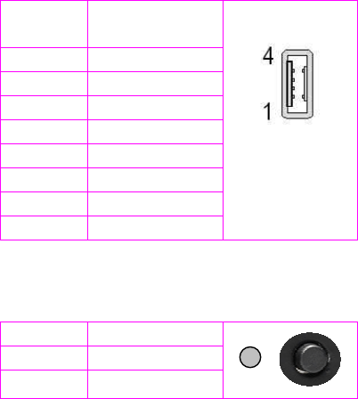
USB
J6: USB-90 / 4-pin USB Type 1 Connector (USB-90 / Vertical Type)
Pin # Signal
Name
1 VCC
2 -DATA0
3 +DATA0
4 GND
5 GGND
6 GGND
7 GGND
8 GGND
Power Button (switch)
S2: TACT-SW-90 / 2-pole TACT-SW-90
Action Status
Push ON
No push
Stay As Is

53
APPENDIX B: AVL POWER MANAGEMENT
S1: Auto Power Voltage Selection / 4-pin SW DIP-2-SMD
Status Voltage Selection
Pin# Signal
Name VS1 VS2 ±12V ±24V
1 GND OFF OFF 13V 26V
2 GND OFF ON 13.2V 26.4V
3 VS1 ON OFF 13.4V 26.8V
4 VS2 ON ON 13.6V 27.2
Status Description
1 Auto Detect 12V/24V Volt Power On
2 Switch Power On/Off
3 Temperature Sensor Input
4 Battery Volt Detect
5 Isolate Input Detect x4
6 Wake On Timer Counter
7 Wake On / Ring (GPRS)
8 Wake On Isolate Input x4
9 LED Display Wake Up Status
10 DIP Switch Select Power On Volt Detect Level
11 Software Control Power Off
12 I2C Interface Communication
54
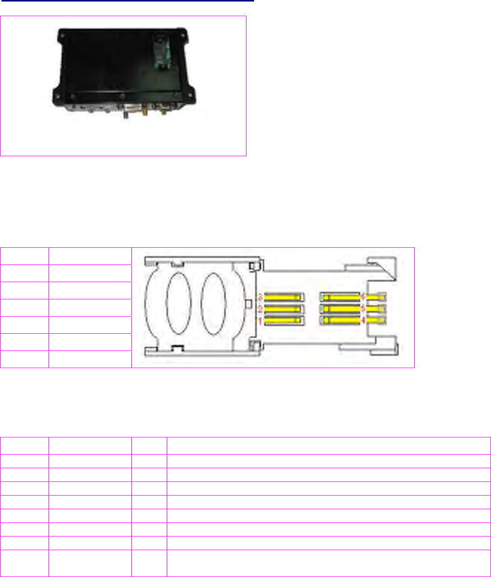
APPENDIX C: SIM CARD HOLDER
Figure D1 : SIM Card location
(Beneath the encasing)
Note: The SIM card holder for GSM is situated and can be found beneath the encasing.
Flip-up the system upside down, on the upper right position of the case, unlock a stamp
plate.
TABLE D1 : Pin numbers of Molex SIM card holder on DSB45 Support Box
J16: SIM CARD HOLDER 3x2-2.54mm
PIN# Signal Name
1 SIM-VCC
2 SIM-RST
3 SIM-CLK
4 SIM-GND
5 SIM-VPP
6 SIM-IO
Note: Pins 1 through 8 (except for 5) are the minimum requirement according to the GSM
Recommendations, where pins 7 and 8 are needed for SIM card tray detection through the
CCIN pin.
Table D2 : Other reference Pin assignment of Molex SIM card holder
Status Signal name I/0 Function
1 CCVCC. I Supply voltage for SIM card, generated by the GSM engine
2 CCRST I Chip card reset prompted by the GSM engine
3 CCCLK I Chip card clock
4 CCGND - Individual ground line for the SIM card to improve EMC
5 CCVPP - Not connected
6 CCIO I/O Serial data line, bi-directional
7 CCDET1 - Connect to CCVCC
8 CCDET2 - Connects to the CCIN input of the GSM engine. Serves
to recognize whether a SIM card is in the holder.
55
Limited Warranty
Terms and Conditions
The warranty terms for AVL75 SYSTEM are 12 months beginning on the date of invoice. During the
warranty period, DMP will repair replace the commodity covered under this limited warranty.
DMP warrants the hardware and software COMMODITIES are manufactured and produced to be free
from defects in the materials and workmanship for one year following the date of shipment from DMP.
This warranty is limited to the original purchaser of product and is not transferable.
The warranty does not apply to:
Product that has been installed incorrectly, this specifically includes but is not limited to
cases where electrical short circuit is caused.
Product that has been altered or repaired except by the manufacturer (or with the
manufacturer’s consent).
Product that has subjected to misuse, accidents, abuse, negligence or unusual stress
whether physical or electrical.
Ordinary wear and tear.
Service and Support
DMP provides the technical support for software and hardware problems with your system
throughout the warranty period. The technical support service is limited to configuration and
operation of AVL75 COMMODITY sold by DMP. The technical support service does not offer software
tutoring or training.
During the one-year warranty period, DMP will repair or replace, at its option, any defective products
or parts at no additional charge, provided that the product is returned, shipping prepaid, to DMP. All
replaced parts and products become the property of DMP. Before returning any product for repair,
customers are required to contact the factory for an RMA number.
This Limited Warranty does not extend to any products which have been damaged as a result of
accident, misuse, abuse (such as: use of incorrect input voltages, improper or insufficient ventilation,
failure to follow the operating instructions that are provided by DMP, "acts of God" or other
contingencies beyond the control of DMP), or as a result of service or modification by anyone other
than DMP. Except as expressly set forth above, no other warranties are expressed or implied,
including, but not limited to, any implied warranties of merchantability and fitness for a particular
purpose, and DMP expressly disclaims all warranties not stated herein. All implied warranties,
including implied warranties for merchantability and fitness for a particular purpose, are limited to
the duration of this warranty. In the event the product is not free from defects as warranted above,
the purchaser’s sole remedy shall be repair or replacement as provided above, under no
circumstances will DMP be liable to the purchaser or any user for any damages, including any
incidental or consequential damages, expenses, lost profits, lost savings, or other damages arising
out the use or inability to use the product.
Limitation of Liability
The manufacturer’s liability for damages to customer or others resulting from the use of any product
supplied hereunder shall in no event exceed the purchase price of said product.

56
Return Policy
Return Merchandise Authorization(RMA)policy
If DMP’s technical support staff determines that a part is defective. Purchaser must call our
technical support service to obtain an RMA number before attempting to return any part.
To obtain an RMA number, Purchaser must follow procedures as below:
1. Complete the DMP’s standard RMA Form and fax back to the RMA Department.
2. The RMA Number must be used within 7 DAYS
3. The RMA Number must be shown clearly on your shipping label.
4. DMP must receive all Returns before a replacement will be sent.
5. The repair cost depends on the parts, the damage reasons, and whether under
warranty period…etc. The Seller will charge the Purchaser in a reasonable price.
6. A copy of the invoice for the RMA product(s) will also be shipped to Purchaser.
7. The freight of return to DMP is charge to the Purchaser account and accompanied by an
RMA number. Any Returns with freight collect will be refused and returned to you.
After Repairing, the cost of freight will be paid by Seller.
8. DMP must receive all returned goods within the warranty period.
Shipping Policy
The Purchaser must pre-pay the shipping cost for any defective system or parts returned under the
warranty. DMP shall not be liable for risk of loss or damage during shipment of your returned
system or parts if you fail to insure the shipment.
All products must be shipped back to DMP in original or equivalent packaging. DMP will shipped the
repaired or replacement product(s) to Purchaser by freight prepaid. Purchaser assumes the risk of
loss. DMP shall not be responsible for failure of the delivery service to make on-time delivery.
Ship the package to:
ATTN: DMP ELECTRONICS INC.
TO: 8F, No.12, Wu-Quan 7 Rd.,
Wu Gu Industrial Park,
Wu Gu Xiang, Taipei #248,
TAIWAN, R.O.C.
RMA xxxxxxxx
Attention: Failure to follow this return procedure will almost always delay repair! Please help us
expedite your repair by following this procedure.
WEBSITE
www.avl.tw
Specifications subject to change without notice
Technical Guide for AVL75 v0r7.doc © DMP Electronics Inc. 2006
First issued date: 30 March, 2006, Last issued date: 21 June, 2007
CONTACT DETAILS
DMP has offices in Asia, Europe and USA with corresponding internet site: Please check with
macarios@avl.tw for assistance.