DXY Technology 021 DXY BLE MODULE User Manual DXYBT021 v1 1
DXY Technology Co.,Ltd. DXY BLE MODULE DXYBT021 v1 1
User Manual
DXYBT021
OEM/INTEGRATORS
INSTALLATIONS MANUAL
www.dxytech.com Tel:400-9900-108 1/7
VERSION HISTORY
Version
Comment
V1.0
First draft
V1.1
Add new pin out and modify some description
www.dxytech.com Tel:400-9900-108 2/7
1 Description
The DXYBT021 is a compact, surface mount Bluetooth 4.0 Low Energy (BLE) compliant wireless
module. It integrates an advanced single-chip BLE SoC chip-QN9021 with RF circuit and antenna
in a compact module.
Due to its small size, outstanding performance at very low power consumption and easy modular
handling, the DXYBT021 is leading the way for the new generation of Bluetooth low energy
modules.
2 Key Features
◆Bluetooth®4.0 Low Energy wireless module
●Frequency bands:2400MHz to 2483.5MHz
● 1Mbps on air data rate
● Slave and Master mode operation
● Support to 8 simultaneous links in master mode
◆Integrated 32-bit Cortex-M0 MCU with
●64K system memory
●64/128KB falsh
◆Ultra Low Power Consumption
● 2uA deep sleep mode
● 3uA sleep mode(32kHz RC OSC on)
● DC-DC mode
8.9mA RX current at 3V
8.8mA TX current @0dBm Tx power at 3V
●Non DC-DC mode
13.6mA RX current at 3V
13.3mA TX current @0dBm Tx power at 3v
●Integrated DC-DC converter and LDO
●Single 2.4V-3.6V power supply
◆High Performance
●-95dBm RX sensitivity (Non DC‐DC mode)
●-93dBm RX sensitivity (DC‐DC mode)
●Tx power from ‐20dBm to 4dBm
●Excellent link budget up to 99dB
◆Complete Protocol Stack and Profile
●Bluetooth® v4.0 host stack including L2CAP , SMP, ATT, GATT, GAP
●Qualified application profiles and services
◆Ease of Design
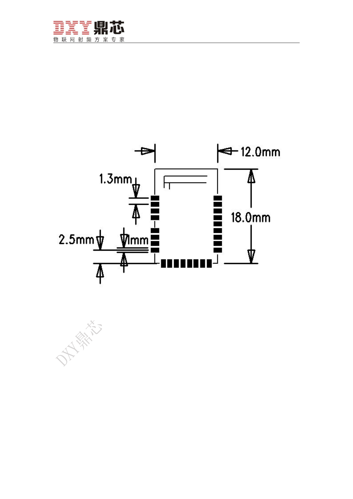
●Small form factor: 12x18x2mm
www.dxytech.com Tel:400-9900-108 3/7
●Easy to use command set over UART/SPI to communicate with App MCU
◆Application
●Sports & Fitness
●Healthcare & Wellness
●Remote Control
●PC Peripherals (mouse, keyboard)
●Mobile Phone Accessories
●Home/building Automation
●Industrial automation
●Wireless Sensor Networks
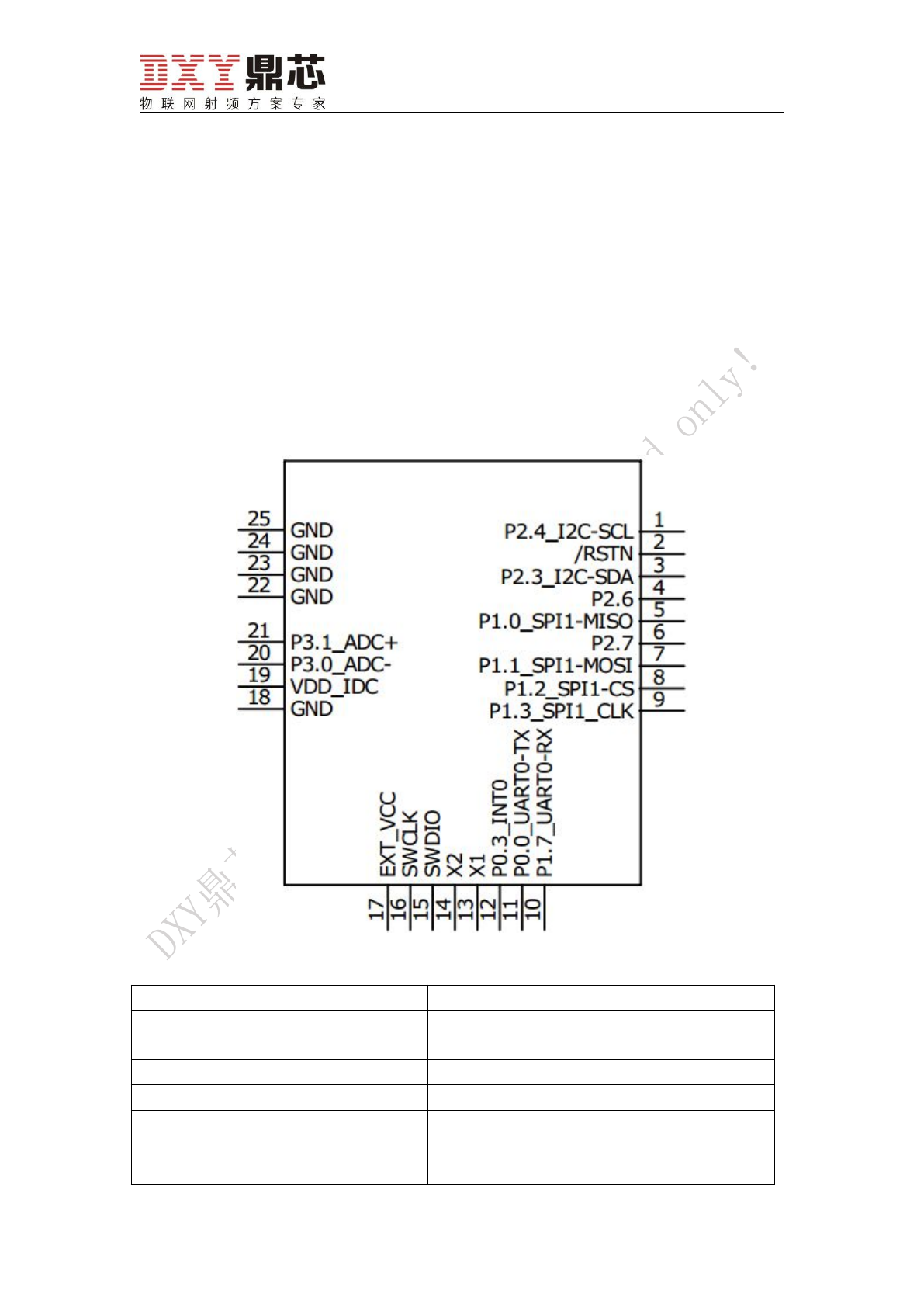
3 Pin out
Table 1 Pin out description
Pin
Name
Function
Description
1
P2.4/I2C_SCL
Digital in/out
GPIO / I2C clock
2
/RSTN
Digital in/out
Hardware reset, active low.
3
P2.3/I2C_SDA
Digital in/out
GPIO / I2C data with pull-up
4
P2.6
Digital in/out
GPIO
5
P1.0/SPI_MISO
Digital in/out
GPIO / SPI data master in/slave out
6
P2.7
Digital in/out
GPIO
7
P1.1/SPI_MOSI
Digital in/out
GPIO / SPI data master out/slave in
www.dxytech.com Tel:400-9900-108 4/7
8
P1.2/SPI_CS
Digital in/out
GPIO / SPI chip select
9
P1.3/SPI_CLK
Digital in/out
GPIO / SPI clock
10
P1.7/UART_RX
Digital input
GPIO / UART RX data input
11
P0.0/UART_TX
Digital output
GPIO / UART TX data output
12
P0.3/INT0
Digital in
GPIO / Interrupt
13
X1
Analog in
Not connected
14
X2
Analog in
Not connected
15
SWDIO
Digital in/out
SWD data with pull-up
16
SWCLK
Digital in
SWD clock input with pull-up
17
VCC
Power
Power supply (2.4~3.6V)
18
GND
Ground
Should be connected to ground
19
VDD_IDC
Power
Not connected
20
P3.0/ADC-
Analog in
GPIO / ADC-
21
P3.1/ADC+
Analog in
GPIO / ADC+
22
GND
Ground
Should be connected to ground
23
GND
Ground
Should be connected to ground
24
GND
Ground
Should be connected to ground
25
GND
Ground
Should be connected to ground
4 Electrical Characteristics
Table 2 Recommended Operating Conditions
Symbol
Parameter
Conditions
Min
Typ
Max
Unit
VCC
Power
To GND
2.4
3.0
3.6
V
TA
Operating temperature
-40
+25
+85
℃
Table 3 DC Characteristics
Symbol
Parameter
Conditions
Min
Typ
Max
Unit
Icc
Current consumption
Deep sleep
2
uA
Sleep
3
uA
Idle(w/o DC-DC)
0.84
mA
MCU@8MHz(w/o DC-DC)
1.35
mA
Rx(w/o DC-DC)
13.6
mA
Rx(w/t DC-DC)
8.9
mA
(Typical values are Ta=25℃and VCC=3V)
Notes:
1. Current include current for both analog and digital;
2. Depend on IO conditions.
3. Deep sleep mode: digital regulator off, no clocks, POR, RAM/register content retained
4. Sleep mode: digital regulator off, 32k RC OSC on, POR, sleep timer on, and RAM/register
content retained
5. Idle: 16MHz OSC on, no radio or peripherals, 8 MHz system clock and MCU idle (no code
www.dxytech.com Tel:400-9900-108 5/7
execution)
6. MCU@8 MHz: MCU running at 8 MkHz RC OSC clock, no radio or peripherals
7. RX sensitivity is -95dBm sensitivity when DC-DC is disabled.
8. RX sensitivity is -93dBm sensitivity when DC-DC is enabled.
5 Layout and physical dimemsions
Full Modular Approval
This RF Module is full modular approval, it is limited to OEM installation ONLY.
Integration into devices that are directly or indirectly connected to AC lines must add with Class II
Permissive Change. (OEM) Integrator has to assure compliance of the entire end product incl. the
integrated RF Module. Additional measurements (15B) and/or equipment authorizations (e.g
Verification) may need to be addressed depending on co-location or simultaneous transmission
issues if applicable. (OEM) Integrator is reminded to assure that these installation instructions
will not be made available to the end user of the final host device.
With the documented max output power this RF Module meets the FCC SAR Exemption, so it
comply with any applicable RF exposure requirements in its final configuration. The RF Module is
powered by battery, the antenna is PCB antenna and the antenna gain is 2.21dBi. The final host
device, into which this RF Module is integrated" has to be labeled with an auxiliary label stating
www.dxytech.com Tel:400-9900-108 6/7
the FCC ID of the RF Module, such as “Contain FCC ID: 2AEZC021"."
The module is limited to installation in mobile or fixed applications. The separate approval is
required for all other operating configurations, including portable configuration with respect to
Part 2.1093 and different antenna configurations.
FCC RF Statement
This device complies with part 15 of the FCC rules. Operation is subject to the following two
conditions: (1) this device may not cause harmful interference, and (2) this device must accept
any interference received, including interference that may cause undesired operation.
NOTE: The manufacturer is not responsible for any radio or TV interference caused by
unauthorized modifications to this equipment. Such modifications could void the user’s authority
to operate the equipment.
NOTE: This equipment has been tested and found to comply with the limits for a Class B digital
device, pursuant to part 15 of the FCC Rules. These limits are designed to provide reasonable
protection against harmful interference in a residential installation. This equipment generates
uses and can radiate radio frequency energy and, if not installed and used in accordance with the
instructions, may cause harmful interference to radio communications. However, there is no
guarantee that interference will not occur in a particular installation. If this equipment does
cause harmful interference to radio or television reception, which can be determined by turning
the equipment off and on, the user is encouraged to try to correct the interference by one or
more of the following measures:
- Reorient or relocate the receiving antenna.
- Increase the separation between the equipment and receiver.
-Connect the equipment into an outlet on a circuit different from that to which the receiver is
connected.
-Consult the dealer or an experienced radio/TV technician for help
- This device and its antenna(s) must not be co-located or operating in conjunction with any other
antenna or transmitter.
Hereby, DXY Technology Co.,Ltd. declares that this device is in compliance with the essential
requirements and other relevant provisions of Directive 1999/5/EC.
For the declaration of conformity, visit the Web site http://www.dxytech.com
Notice: Observe the national local regulations in the location where the device is to be used. This
device may be restricted for use in some or all member states of the European Union (EU)