Datalogic S r l RHINOIIWEC7 802.11abgn M.2 module w/SDIO interface User Manual Rev 02 171030
Datalogic S.r.l. 802.11abgn M.2 module w/SDIO interface Rev 02 171030
User Manual-Rev.02(171030)

A
Datasheet
M2SD50NBT

M2SD50NBT
Datasheet
2
CONTENTS
1
Scope.................................................................................................................................................................3
2
Specifications.....................................................................................................................................................3
3
WLANFunctionalDescription...........................................................................................................................5
3.1
Overview................................................................................................................................................5
4
BluetoothFunctionalDescription.....................................................................................................................7
5
ElectricalCharacteristics...................................................................................................................................8
5.1
AbsoluteMaximumRatings...................................................................................................................8
5.2
RecommendedOperatingConditions...................................................................................................8
5.3
DCElectricalCharacteristics...................................................................................................................8
5.4
WLANRadioReceiverCharacteristics..................................................................................................10
6
BluetoothRadioCharacteristics......................................................................................................................11
7
SDIOTimingRequirements.............................................................................................................................13
8
PinDefinitions.................................................................................................................................................14
9
MechanicalSpecifications...............................................................................................................................17
10
Mounting.........................................................................................................................................................17
11
RFLayoutDesignGuidelines/Precautions.......................................................................................................19
12
Regulatory.......................................................................................................................................................20
12.1
CertifiedAntennas...............................................................................................................................20
13
FCCandICRegulatory.....................................................................................................................................21
13.1
FCC.......................................................................................................................................................21
13.1.1
FederalCommunicationCommissionInterferenceStatement........................................21
13.1.2
EndProductLabeling........................................................................................................22
13.1.3
ManualInformationtotheEndUser...............................................................................22
13.2
IndustryCanada...................................................................................................................................22
13.2.1
IndustryCanadaStatement..............................................................................................22
13.2.2
AntennaInformation........................................................................................................23
13.2.3
RadiationExposureStatement.........................................................................................24
13.2.4
Déclarationd'expositionauxradiations...........................................................................24
13.2.5
EndProductLabeling........................................................................................................25
13.2.6
Plaquesignalétiqueduproduitfinal................................................................................25
13.2.7
ManualInformationtotheEndUser...............................................................................25
13.2.8
Manueld'informationàl'utilisateurfinal........................................................................25
M2SD50NBT
Datasheet
3
1 SCOPE
ThisdocumentdescribeskeyhardwareaspectsoftheLairdM2SD50NBTmodule.Thisdocumentisintendedto
assistdevicemanufacturersandrelatedpartieswiththeintegrationofthisradiointotheirhostdevices.Datain
thisdocumentisdrawnfromanumberofsourcesandincludesinformationfoundintheLairdSSD50NBTwhich
includingQualcommAtheros(QCA)QCA6004andCambridgeSiliconRadioLtd.(CSR)CSR8811A08datasheet
issuedinJuly2011,alongwithotherdocumentsprovidedfromQCAandCSR
Notethattheinformationinthisdocumentissubjecttochange.PleasecontactLairdtoobtainthemostrecent
versionofthisdocument.
2 SPECIFICATIONS
Table1:Specifications
FeatureDescription
Wi‐FiInterface1‐bitor4‐bitSecureDigitalI/O
BluetoothInterfaceHostControllerInterface(HCI)usingHighSpeedUART
MainChip Wi‐Fi–QualcommAtherosQCA6004
BT–CambridgeSiliconRadioLtd.(CSR)CSR8811A08
InputVoltageRequirements3.3VDC(3.20Vminto3.46Vmax)
I/OSignallingVoltage3.3VDC±5%or1.8VDC±5%
OperatingTemperature‐30°to85°C(‐22°to185°F)
OperatingHumidity10to90%(non‐condensing)
StorageTemperature‐40°to85°C(‐40°to185°F)
StorageHumidity10to90%(non‐condensing)
Size22mmX30mmX3.3mm(.87”x1.18”x.13”)
Weight<3.0grams(<0.105822ounces)
Wi‐FiStandardsIEEE802.11a,802.11b,802.11d,802.11e,802.11g,802.11h,802.11i,
802.11n,802.11r
BluetoothStandardsBluetoothversion2.1withEnhancedDataRate
Bluetooth4.0(BluetoothLowEnergyorBLE)
Wi‐FiDataRatesSupported 11a(OFDM)6,9,12,18,24,36,48,54Mbps
802.11b(DSSS,CCK)1,2,5.5,11Mbps
802.11g(OFDM)6,9,12,18,24,36,48,54Mbps
802.11n(OFDM,MCS0‐15)
FullGuardInterval:6.5,13.0,19.5,26.0,39.0,52.0,58.5,65.0,13.0,26.0,39.0,
52.0,78.0,104.0,117.0Mbps
ShortGuardInterval:1.2,14.4,21.7,29.9,43.3,57.8,65.0,72.2,
14.4,28.9,43.3,57.8,86.7,115.6,130.0,144.4Mbps
M2SD50NBT
Datasheet
4
FeatureDescription
ModulationBPSK@1,6,9,6.5,7.2,13and14.4Mbps
QPSK@2,12,18,13,14.4,19.5,21.7,26,28.9,39,43.3Mbps
CCK@5.5and11Mbps
16‐QAM@24,36,26,29.9,39,43.3,52,57.8,78,86.7Mbps
64‐QAM@48,54,52,57.8,58.5,65,72.2,104.0,115.6,117.0,130.0,144.4
Mbps
802.11nSpatialStreams2(2x2MIMO)
BluetoothDataRates
Supported1,2,3Mbps
BluetoothModulationGFSK@1Mbps
Pi/4‐DQPSK@2Mbps
8‐DPSK@3Mbps
RegulatoryDomainSupport FCC(Americas,PartsofAsia,andMiddleEast)
ETSI(Europe,MiddleEast,Africa,andPartsofAsia)
IC(IndustryCanada)
MIC(Japan)(formerlyTELEC)–Option
KC(Korea)(formerlyKCC)–Option
2.4GHzFrequencyBandsETSI:2.4GHzto2.483GHz
FCC:2.4GHzto2.473GHz
MIC:2.4GHzto2.495GHz
KC:2.4GHzto2.483GHz
2.4GHzOperatingChannels
(Wi‐Fi)
ETSI:13(3non‐overlapping)
FCC:11(3non‐overlapping)
MIC:14(4non‐overlapping)
KC:13(3non‐overlapping)
5GHzFrequencyBands
ETSI
5.15GHzto5.35GHz(Ch36/40/44/48/52/56/60/64)
5.47GHzto5.725GHz(Ch
100/104/108/112/116/120/124/128/132/136/140)
FCC
5.15GHzto5.35GHz(Ch36/40/44/48/52/56/60/64)
5.47GHzto5.725GHz(Ch
100/104/108/112/116/120/124/128/132/136/140
5.725GHzto5.825GHz(Ch149/153/157/161/165)
MIC(Japan)
5.15GHzto5.35GHz(Ch36/40/44/48/52/56/60/64)
5.47GHzto5.725GHz(Ch
100/104/108/112/116/120/124/128/132/136/140)
KC
5.15GHzto5.35GHz(Ch36/40/44/48/52/56/60/64)
5.47GHzto5.725GHz(Ch100/104/108/112/116/120/124)
5.725GHzto5.825GHz(Ch149/153/157/161)

M2SD50NBT
Datasheet
5
FeatureDescription
5GHzOperatingChannels
(Wi‐Fi)
ETSI:19non‐overlapping
FCC:24non‐overlapping
MIC:(Japan):19non‐overlapping
KC:19non‐overlapping
CertificationsWi‐FiAlliance
802.11a,802.11b,802.11g,802.11n
WPAEnterprise
WPA2Enterprise
CiscoCompatibleExtensions(Version4)
Bluetooth SIGQualification
WarrantyThreeYearWarranty
Allspecificationsaresubjecttochangewithoutnotice
3 WLANFUNCTIONALDESCRIPTION
3.1 Overview
TheM2SD50NBTWLANblockisbasedontheLairdSSD50NBTSIP(SysteminPackage).Itisoptimizedforlow‐
powerembeddedapplicationsandisconfiguredtooperateindual‐band,two‐stream(2x2MIMO)mode.Its
functionalityincludes:
Improvedthroughputonthelinkduetoframeaggregation,RIFS(reducedinter‐framespacing),andhalf‐
guardintervals.
SupportforSTBC(space‐timeblockcoding)andLDPC(LowDensityParityCheck)codes.
Improved11nperformanceduetofeaturessuchas11nframeaggregation(A‐MPDUandA‐MSDU)and
low‐overheadhost‐assistedbuffering(RXA‐MSDUandRXA‐MPDU).Thesetechniquescanimprove
performanceandefficiencyofapplicationsinvolvinglargebulkdatatransferssuchasfiletransfersorhigh‐
resolutionvideostreaming.
M2SD50NBT
Datasheet
6
Otherfunctionalityincludesthefollowing:
FeatureDescription
SystemClocking
(RTCBlock)
AnRTCblockcontrolstheclocksandpowergoingtootherinternalmodules.Itsinputs
containsleeprequestsfromthesemodulesanditsoutputscontainclockenableand
powersignalswhichareusedtogatetheclocksgoingtothesemodules.TheRTCblock
alsomanagesresetsgoingtoothermoduleswiththedevice.TheM2SD50NBT’sclockingis
groupedintotwotypes:high‐speedandlow‐speed.
3.1.1.1 HighSpeedClocking
Thereference26MHzclocksourcedrivesthePLLandRFsynthesizerofWi‐Fiand
Bluetooth.Tominimizepowerconsumption,thereferenceclocksourceispoweredoffin
SLEEP,HOST_OFF,andOFFstates.
3.1.1.2 LowSpeedClocking
Thismodulerequiresanexternalsleepclock(32.768KHz)sourcefromhostplatform
throughpin‐50ontheNFGGgoldenfinger.ItisusedtoplaceBTintodeepsleepmode.For
Wi‐Fionlyapplication,itisnotneeded.
3.1.1.3 InterfaceClock
ThehostinterfaceclockrepresentsanotherclockdomainfortheM2SD50NBT.Thisclock
comesfromtheSDIOandisindependentfromtheotherinternalclocks.Itdrivesthehost
interfacelogicaswellascertainregisterswhichcanbeaccessedbythehostinHOST_OFF
andSLEEPstates.
MAC/BB/RFBlock
TheM2SD50NBTWirelessMACconsistsoffivemajorblocks:
Hostinterfaceunit(HIU)forbridgingtotheAHBforbulkdataaccessesandAPBfor
registeraccesses
Tenqueuecontrolunits(QCU)fortransferringTXdata
TenDCFcontrolunits(DCU)formanagingchannelaccess
Protocolcontrolunit(PCU)forinterfacingtobaseband
DMAreceiveunit(DRU)fortransferringRXdata
BasebandBlock
TheM2SD50NBTbasebandblock(BB)isthephysicallayercontrollerforthe802.11b/g/n
airinterface.
Itmodulatesdatapacketsinthetransmitdirection
Detectsanddemodulatesdatapacketsinthereceivedirection.
Ithasadirectcontrolinterfacetotheradiotoenablehardwaretoadjustanaloggains
andmodesdynamically.
ClockSharing
ClocksharingisimplementedontheM2SD50NBT.TheBluetoothchip(CSR8811)
receivesareferenceclockfromtheWi‐Fichip(QCA6004).WhenWi‐Fiisinpower
off/resetstate,Bluetoothisalsooff.
External32.768KHzsignalpresentonpin50allowstheBTchiptogointodeepsleep
modeandconsumelowestamountofpower
M2SD50NBT
Datasheet
7
4 BLUETOOTHFUNCTIONALDESCRIPTION
TheM2SD50NBTBluetooth(BT)blockisbasedontheCSR8811A08anddescribedintheTable2.
Table2:Bluetoothfunctions
FeatureDescription
HCI‐UARTInterfaceTheUARTInterfaceisastandardhigh‐speedUARTinterface.Itoperatesupto4Mbps,
supportingBluetoothHCIUARTinterface.
PCMorI2SInterface
ContinuousPCMencodedaudiodatatransmissionandreceptionoverBluetooth
Processoroverheadreductionthroughhardwaresupportforcontinual
transmissionandreceptionofPCMdata
Abi‐directionaldigitalaudiointerfacethatroutesdirectlyintothebasebandlayer
ofthefirmware.ItdoesnotpassthroughtheHCIprotocollayer
HardwareonCSR8811forsendingdatatoandfromaSCOconnection
UptothreeSCOconnectionsonthePCMinterfaceatanyonetime
PCMinterfacemaster,generatingPCM_SYNCandPCM_CLK
PCMinterfaceslave,acceptingexternallygeneratedPCM_SYNCandPCM_CLK.
Variousclockformatsincluding:
– *LongFrameSync
– *ShortFrameSync
GCItimingenvironments
13‐bitor16‐bitlinear,8‐bitμ‐laworA‐lawcompandedsampleformats
Receivesandtransmitsonanyselectionofthreeofthefirstfourslotsfollowing
PCM_SYNC
ThePCMconfigurationoptionsareenabledbysettingSKEY_PCM_CONFIG32
CPUandMemory
Usesa16‐bitRISCMCUforlowpowerconsumptionandefficientuseofmemory.
TheMCU,interruptcontroller,andeventtimerruntheBluetoothsoftwarestack
andcontroltheBluetoothradioandhostinterfaces.
56KBofon‐chipRAMisprovidedtosupporttheRISCMCUandissharedbetween
theringbuffersusedtoholdvoice/dataforeachactiveconnectionandthe
general‐purposememoryrequiredbytheBluetoothstack.
5MbofInternalROMmemoryisavailableontheCSR8811.Thismemoryis
providedforsystemfirmware,storingCSR8811settingsandprogramcode.
Build‐inStandard
WLANCoexistence
TheM2SD50NBTinternallysupportsthestandardWLANcoexistenceinterface
throughtheWLAN_ACTIVE,BT_PRIORITY,andBT_ACTIVEpins.
ReferenceClock
TheBTblockisconfiguredfor26MHzreferenceclockfrequency.Theclocksourceis
providedtoBTinternallyfromtheWLANblockondemandfromBT_CLK_REQ.
Note:TheWLANblockmustbeinitializedpriorbeforeBTclocksharingisenabled.
BTLowEnergy
SupportsLowEnergyspecificationwhichallowsforconnectionstodeviceswithsingle
modeLEfunction(suchasawatch,sensor,andHID).Theimplementationisoptimized
forcoexistencewithWLAN.
BT_RFKILL
TheNGFFpin‐54isconnectedto(BT_PWD_L)resetsandpowersdowntheBTblock.
Holdingthepin‐54atLowstateturnsofftheentireBTblock;allstateinformationis
lost.Toensureafullreset,theresetsignalshouldbeassertedforaperiodgreater
thanfivemilliseconds.
M2SD50NBT
Datasheet
8
FeatureDescription
Radio
TheBTradiosharesthesingleantennaportwiththeWLANthroughaninternalthree‐
wayRFswitch.TheM2SD50NBTimplementsWLAN/BTcoexistenceinternally.
VDDIOistosettheI/Ovoltageinternallywitheither1.8Vor3.3Vtoensuresame
voltagelevelfortheinternalWi‐FiandBTcoexistencesignal.Refertothereference
designspecificationsfordetails.
5 ELECTRICALCHARACTERISTICS
5.1 AbsoluteMaximumRatings
Table3summarizestheabsolutemaximumratingsandTable4liststherecommendedoperatingconditionsfor
the
M2SD50NBT
.Absolutemaximumratingsarethosevaluesbeyondwhichdamagetothedevicecanoccur.
Functionaloperationundertheseconditions,oratanyotherconditionbeyondthoseindicatedinthe
operationalsectionsofthisdocument,isnotrecommended.
Note:Maximumratingforsignalsfollowsthesupplydomainofthesignals.
Table3:AbsoluteMaximumRatings
Symbol(Domain) Parameter MaxRatingUnit
VDDIO WLANhostSDIOinterfaceandBTI/Osupply ‐0.3to3.6V
VCC3_3External3.3Vpowersupply ‐0.3to3.6V
StorageStorageTemperature ‐40to+85°C
ANT1;ANT2MaximumRFinput(referenceto50‐Ωinput) +10dBm
ESD Electrostaticdischargetolerance 2000V
5.2 RecommendedOperatingConditions
Table4:RecommendedOperatingConditions
Symbol(Domain) Parameter MinTypMaxUnit
VDDIO WLANhostinterfaceandBTI/Osupply1.71/3.2 1.8/3.31.89/3.46 V
VCC3_3 External3.3Vpowersupply 3.23.303.46V
T‐ambient Ambienttemperature ‐302585°C
5.3 DCElectricalCharacteristics
Table5andTable6listthegeneralDCelectricalcharacteristicsoverrecommendedoperatingconditions(unless
otherwisespecified).
Table5:GeneralDCElectricalCharacteristics(For3.3VI/OOperation)
SymbolParameterConditionsMinTypMaxUnit
VIHHighLevelInputVoltage 0.7xVDD V
VILLowLevelInputVoltage 0.3x
VDDV
IIL
Input
Leakage
Current
WithoutPull‐up
orPull‐down
0V<VIN<VDD
0V<VOUT<VDD0‐3nA
WithPull‐up0V<VIN<VDD
0V<VOUT<VDD16 48µA
M2SD50NBT
Datasheet
9
SymbolParameterConditionsMinTypMaxUnit
WithPull‐down0V<VIN<VDD
0V<VOUT<VDD‐14 ‐47µA
VOHHighLevelOutputVoltageIOH=‐4mA0.9xVDD V
IOH=‐12mA0.9xVDD V
VOLLowLevelOutputVoltage
IOH=4mA
0.1x
VDDV
IOH=12mA
0.1x
VDDV
Table6:GeneralDCElectricalCharacteristics(For1.8VI/OOperation)
SymbolParameterConditions Min TypMaxUnit
VIHHighLevelInputVoltage 0.7xVDD V
VILLowLevelInputVoltage 0.3xVDD V
IILInput
Leakage
Current
WithoutPull‐up
orPull‐down
0V<VIN<VDD
0V<VOUT<VDD
0‐3nA
WithPull‐up0V<VIN<VDD
0V<VOUT<VDD
3.513µA
WithPull‐down0V<VIN<VDD
0V<VOUT<VDD
‐6.2‐23µA
VOHHighLevelOutputVoltageIOH=‐4mA0.9xVDD V
IOH=‐12mA0.9xVDD V
VOLLowLevelOutputVoltageIOH=4mA0.1xVDD V
IOH=12mA0.1xVDD V
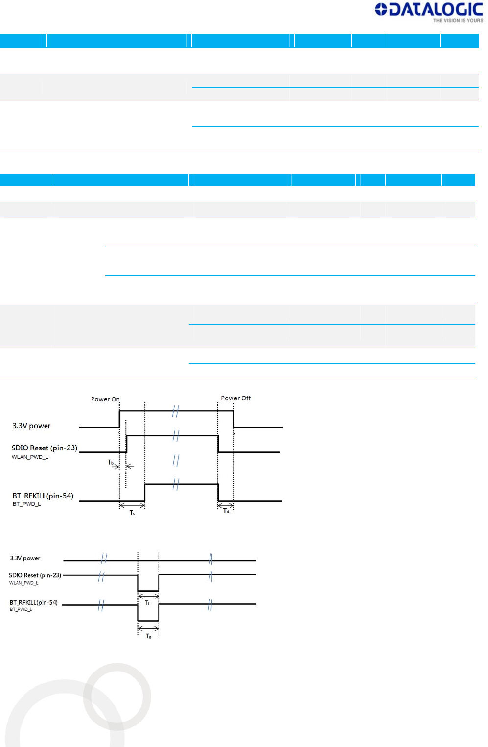
Figure1:PowerOn/OffTiming
Figure2:ResetTiming
M2SD50NBT
Datasheet
10
Table7:TimingDiagramDefinitions
TimingDescriptionMinUnit
TbTimebetweenVDD33(3.3V)suppliesvalid,toSDIOreset(pin‐
56;WLAN_PWD_L)negation.
Note:havesuitable10KohmPull‐uponSDIObus,already.Noextra
pull‐upresistorisrequired.
5µsec
TcTimebetweenVDD33(3.3V)suppliesvalidand
BT_RFKILL(pin‐54;BT_PWD_L)negation5msec
TdTimebetweenSDIOreset(pin‐56;WLAN_PWD_L)negationand
VDD33(3.3V)invalid,ortimebetweenBT_RFKILL(pin‐54;
BT_PWD_L)negationandVDD33(3.3V)invalid.
0µsec
TfTimeofSDIOreset(pin‐56;WLAN_PWD_L)assertionduringreset
orpowerdownperiod.3.3VshouldkeepON.5µsec
TgTimeofBT_RFKILL(pin‐54;BT_PWD_L)assertionduringresetor
powerdownperiod.3.3VshouldkeepON.5msec
Important: Thereis10KohmpullhighresistoralreadyimplementedonSD_D0,SD_D1,andSD_D3.No
externalpull‐upisrequiredforthosethreelines.
5.4 WLANRadioReceiverCharacteristics
Table8andTable9summarizetheWLANM2SD50NBTreceivercharacteristics.
Table8:WLANReceiverCharacteristicsfor2.4GHzSignalChainOperation
SymbolParameterConditionsMinTypMaxUnit
FrxReceiveinputfrequency
range2.412 2.484GHz
Srf
Sensitivity
CCK,1Mbps
SeeNote3
‐94
dBm
CCK,11Mbps ‐87
OFDM,6Mbps ‐91
OFDM,54Mbps ‐74
HT20,MCS0 ‐91
HT20,MCS7 ‐71
RadjAdjacentchannelrejection
OFDM,6Mbps
SeeNote4
32
dB
OFDM,54Mbps16
HT20,MCS031
HT20,MCS714
3Performancedataaremeasuredundersignalchainoperation.
4Performancedataaremeasuredundersignalchainoperation.
Table9:WLANReceiverCharacteristicsfor5GHzDualChainOperation
SymbolParameterConditionsMin TypMaxUnit
FrxReceiveinputfrequency 5.15 5.825GHz
M2SD50NBT
Datasheet
11
SymbolParameterConditionsMin TypMaxUnit
range
Srf
Sensitivity
OFDM,6Mbps
SeeNote5
‐92
dBm
OFDM,54Mbps ‐74
HT20,MCS0 ‐92
HT20,MCS7 ‐71
HT40,MCS0 ‐86
HT40,MCS7 ‐66
RadjAdjacentchannelrejection
OFDM,6Mbps
SeeNote6
22
dB
OFDM,54Mbps9
HT20,MCS020
HT20,MCS719
5Performancedataaremeasuredundersignalchainoperation.
6Performancedataaremeasuredundersignalchainoperation.
6 BLUETOOTHRADIOCHARACTERISTICS
Table10throughTable11describethebasicratetransmitterperformance,enhanceddatatransmitter
performance,basicratereceiverperformance,enhancedratereceiverperformance,andcurrentconsumption
conditionsat25°C.
Table10:BasicRateTransmitterPerformanceTemperatureat25°C(3.3V)
TestParameter Min Typ Max BTSpec.Unit
MaximumRFOutputPower0.56—–6to+10dBm
FrequencyRange2.4—2.4835 2.4≤f≤2.4835GHz
20dBBandwidth—925—≤1000KHz
AdjacentChannelTXPowerF=F0+2
MHz—–36—≤–20dBm
AdjacentChannelTXPowerF=F0+3
MHz—–42—≤–40dBm
Δf1avgMaximumModulation140165175140<Δf1avg<175KHz
Δf2maxMinimumModulation—135—≥115KHz
Δf2avg/Δf1avg—0.9—≥0.80—
InitialCarrierFrequency—5—≤±75KHz
DriftRate—5—≤20KHz/50µs
Drift(DH1packet)—6—≤25KHz
Drift(DH5packet)—7—≤40KHz
Table11:EnhancedDataRateTransmitterPerformance25°C(3.3V)
TestParameterMin Typ Max BTSpec.Unit
RelativeTransmitPower–136–4to+1dBm
MaxCarrierFrequencyπ/4DQPSK—1—≤±10KHz
M2SD50NBT
Datasheet
12
TestParameterMin Typ Max BTSpec.Unit
Stability|wo|8DPSK—1—
MaxCarrierFrequency
Stability|wi|
π/4DQPSK—1—≤±75KHz
8DPSK—1—
MaxCarrierFrequency
Stability|w0+wi|
π/4DQPSK—2—≤±75KHz
8DPSK—1.5—
RMSDEVMπ/4DQPSK—6—≤20%
8DPSK—6—≤13%
PeakDEVMπ/4DQPSK—16—≤35%
8DPSK—15—≤25%
99%DEVM
π/4DQPSK—12—≤30%
8DPSK—12
—≤20%
EDRDifferentialPhaseEncoding—99—≥99%
AdjacentChannelPower
F≥±3MHz—–60—<–40dBm
F=±2MHz—–28—≤–20dBm
F=±1MHz—–32—≤–26dB
Table12:BasicRateReceiverPerformanceat3.3V
TestParameterMinTypMaxBTSpec.Unit
SensitivityBER≤0.1%—–84‐78≤–70dBm
MaximumInputBER≤0.1%–20 ‐10—≥–20dBm
Carrier‐to‐Interferer
Ratio(C/I)
Co‐Channel——1111
AdjacentChannel(±
1MHz)—‐4/‐200dB
SecondAdjacent
Channel(±2MHz)—‐35/‐28 –30–30dB
ThirdAdjacent
Channel(±3MHz)—‐42–40–40dB
MaximumLevelofIntermodulationInterferers–39 ‐30‐ ≥–39dBm
Table13:EnhancedDataRateReceiverPerformance3.3V
TestParameterMinTypMaxBluetooth
SpecificationUnit
Sensitivity(BER≤0.01%)8DPSK—–76‐71≤–70dBm
M2SD50NBT
Datasheet
13
TestParameterMinTypMaxBluetooth
SpecificationUnit
MaximumInput(BER
≤0.1%)
π/4DQPSK–20——≥–20dBm
8DPSK–20——≥–20dBm
Co‐ChannelC/I(BER≤0.1%)
π/4DQPSK—1013≤±13dB
8DPSK—1820≤±20dB
AdjacentChannelC/I(BER≤
0.1%)
π/4DQPSK— ‐9/‐60≤0dB
8DPSK— ‐3/05≤5dB
SecondAdjacentChannel
C/I(BER≤0.1%)
π/4DQPSK—‐42/‐28 –30≤–30dB
8DPSK—‐28/‐22 –25≤–25dB
ThirdAdjacentChannelC/I
(BER≤0.1%)
π/4DQPSK— ‐45–40≤–40dB
8DPSK— ‐39–33≤–33dB
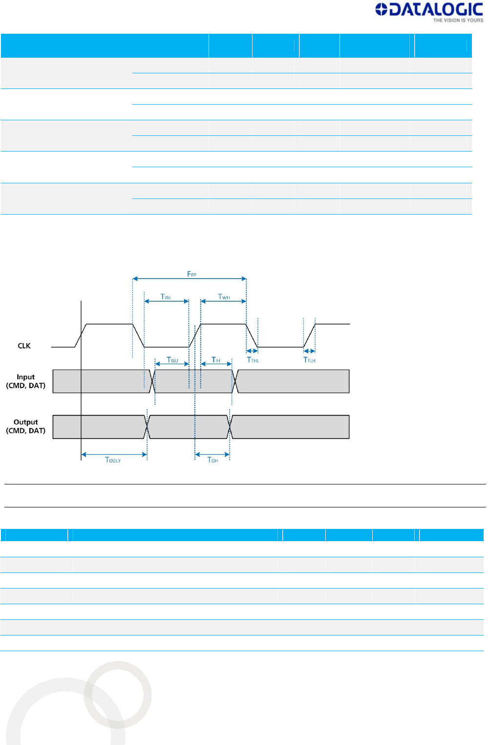
7 SDIOTIMINGREQUIREMENTS
Thefollowingfigure(Figure3)andtabledisplaySDIOdefaultmodetiming.
Figure3:SDIODefaultModeTiming
Note:TimingisbasedonCL≤40pFloadonCMDandData.
Table14:SDIOTimingRequirements
SymbolParameter Min. Typ. Max.Unit
fPPFrequency–DataTransfermode0‐50MHz
tWLClocklowtime7‐ ‐ ns
tWHClockhightime7‐ ‐ ns
tTLHClockrisetime‐ ‐ 10ns
tTHLClocklowtime‐‐10ns
Inputs:CMD,DAT(referencedtoCLK)
tISUInputsetuptime6‐ ‐ ns

M2SD50NBT
Datasheet
14
SymbolParameter Min. Typ. Max.Unit
tIHInputholdtime2‐ ‐ ns
Outputs:CMD,DAT(referencedtoCLK)
tODLYOutputdelaytime–DataTransfermode0‐ 14ns
8 PINDEFINITIONS
Pin#NameTypeVoltage
Reference DescriptionIfNot
Used
1GND‐‐GroundGND
23.3Vaux‐‐3.3Vpowersupply3.3V
3ReservedI/O‐ Reservedpin.Pleaseleaveopen.N/C
43.3Vaux‐‐3.3Vpowersupply3.3V
5ReservedI/O‐ Reservedpin.Pleaseleaveopen.N/C
6LED#1‐‐
ReservedforWi‐FiLEDindicator,
ActiveHigh.
Note:Notsupportedbycurrentsoftware.
N/C
7GND‐‐GroundGND
8BT_PCM_CLKI/O1.8VBTPCMclock N/C
9SDIO_CLKI1.8VWLANSDIOclock
OnlyusedforM2SD50NBT.
N/C
10BT_PCM_SYNCI/O1.8VBTPCMSynchronousdataN/C
11SDIO_CMDI1.8VWLANSDIOcommanddata
OnlyusedonM2SD50NBT.
N/C
12BT_PCM_OUTO1.8VBTPCMsynchronousdataoutputN/C
13SDIO_DATA0I/O1.8VWLANSDIOData0
OnlyusedonM2SD50NBT.
N/C
14BT_PCM_INI1.8VBTPCMsynchronousdatainputN/C
15SDIO_DATA1I/O1.8VWLANSDIOData1
OnlyusedonM2SD50NBT.
N/C
16LED#2‐‐N/CN/C
17SDIO_DATA2I/O1.8VWLANSDIOData2(usedonM2SD50NBT)N/C
18GND‐‐GroundGround
19SDIO_DATA3I/O1.8VWLANSDIOData3(usedonM2SD50NBT)N/C
20BT_UART_WAKEO3.3VReservedforBTtowakeupHost.
WhenBTwakesupfromitsdeepsleep
state,itsendsanHpulsesignalouttoHost.
Normally,itisLowstate.
N/C
21WakeonWLANO1.8VReservedforWake‐ON‐Wireless
(WOW)LAN,WLANoutputsignaltowake
uphost,activeLowandalreadyhasinternal
10Kpullup.
Note:Notsupportedbycurrentsoftware.
N/C

M2SD50NBT
Datasheet
15
Pin#NameTypeVoltage
Reference DescriptionIfNot
Used
22BT_UART_TXDO1.8VBTUARTtransmissiondata.N/C
23WLANresetI1.8VWLANresetorpowerdown;ActiveL
Alreadyhasinternal10Kpull‐up.
HoldthistoLtopowerdowntheWi‐Fichip.
N/C
24MechanicalKey‐E‐ ‐ ‐ ‐
25MechanicalKey‐E‐ ‐ ‐ ‐
26MechanicalKey‐E‐ ‐ ‐ ‐
27MechanicalKey‐E‐ ‐ ‐ ‐
28MechanicalKey‐E‐ ‐ ‐ ‐
29MechanicalKey‐E‐ ‐ ‐ ‐
30MechanicalKey‐E‐ ‐ ‐ ‐
31MechanicalKey‐E‐ ‐ ‐ ‐
32BT_UART_RXDI1.8VBTUARTreceivesdata.N/C
33GND‐‐GroundGND
34BT_UART_RTSO1.8VBTUARTReadytoSend.N/C
35N/C‐‐N/CN/C
36BT_UART_CTSO1.8VBTUARTCleartoSend.N/C
37N/C‐‐N/CNC/
38N/C‐‐N/CN/C
39GND‐‐GroundGND
40N/C‐‐N/CN/C
41N/C‐‐N/CN/C
42N/C‐‐N/CN/C
43N/C‐‐N/CN/C
44LTE_COEX3I1.8VReservedforLTEcoexistence
Note:Notcurrentlysupported.
N/C
45GND‐‐GroundGND
46LTE_ACTIVEI1.8VReservedforLTEcoexistence
Note:Notcurrentlysupported.
N/C
47N/C‐‐N/CN/C
48LTE_FRAME_SYNC I1.8VReservedforLTEcoexistence
Note:Notcurrentlysupported.
N/C
49N/C‐‐ N/CN/C
50CLK_32KI3.3V32.768KHzslowclockinput.
NecessarytoputBTintodeepsleepmode.
N/C
51GND‐‐GroundGND
52N/C‐‐N/CN/C
53N/C‐‐N/CN/C
54BT_RFKILLI3.3VResetBTortodisableBT;ActiveLN/C

M2SD50NBT
Datasheet
16
Pin#NameTypeVoltage
Reference DescriptionIfNot
Used
55N/C‐‐N/CN/C
56WIFI_RFKILLI3.3VReservedforRFdisable(RFKill)feature.
ActiveLow.
Note:Notsupportedbycurrentsoftware.
N/C
57GND‐‐GroundGND
58N/C‐‐N/CN/C
59N/C‐‐N/CN/C
60N/C‐‐N/CN/C
61N/C‐‐N/CN/C
62N/C‐‐N/CN/C
63GND‐‐GroundGND
64N/C‐‐N/CN/C
65N/C‐‐N/CN/C
66N/C‐‐N/CN/C
67N/C‐‐N/CN/C
78N/C‐‐N/CN/C
69GND‐‐GroundGND
70N/C‐‐N/CN/C
71N/C‐‐N/CN/C
723.3Vaux‐‐3.3Vpowersupply3.3V
73N/C‐‐N/CN/C
743.3Vaux‐‐3.3Vpowersupply3.3V
75GND‐‐GroundGND
M2SD50NBT
Datasheet
17
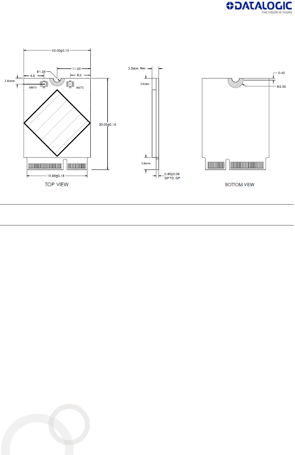
9 MECHANICALSPECIFICATIONS
Figure4:M.2mechanicaldrawings
Note:TheWi‐FiMACaddressislocatedontheproductlabel.TheBTMACaddressisalwaysbenumerically
subsequenttotheWi‐FiMACaddress.Therefore,theBTMACaddressisWi‐FiMACaddressplusone.
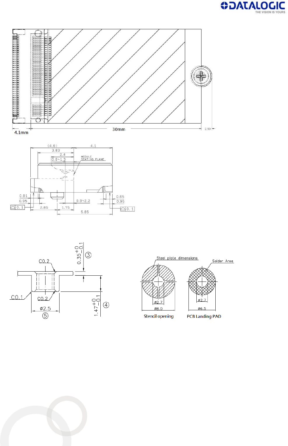
10 MOUNTING
TheM2SD50NBTconnectstothehostviaastandardPCIEXPRESSM2connector.
Kyocera’s(www.Kyocera‐connector.com)6411seriesprovide1.8mm,2.3mmand3.2mmconnectorheights.
M2SD50NBTisasignal‐sidecomponentmodule;Lairdrecommendspartnumber
24‐6411‐067‐101‐897Ewhichhas2.3mmconnectorheight.
Thestand‐offmatingtotherecommend2.3mmconnectorfromEMISTOP(www.EMISTOP.com)ispartnumber
F50M16‐041525P1D4M.DetaillayoutandstencilopeningareshowinFigure5.
M2SD50NBT
Datasheet
18
Figure5:MountinginformationforM2SD50NBTandrecommendedlandpadforstand‐off

M2SD50NBT
Datasheet
19
11 RFLAYOUTDESIGNGUIDELINES/PRECAUTIONS
ThefollowingisalistofRFlayoutdesignguidelinesandrecommendationwheninstallingaLairdradiointoyour
device.
Donotrunantennacablesdirectlyaboveordirectlybelowtheradio.
Donotplaceanypartsorrunanyhighspeeddigitallinesbelowtheradio.
Ifthereareotherradiosortransmitterslocatedonthedevice(suchasaBluetoothradio),placethedevices
asfarapartfromeachotheraspossible.Also,makesurethereareatleast25dBisolationbetween
BluetoothantennaandWi‐Fiantenna.
Lairdrecommendstheuseofadoubleshieldedcablefortheconnectionbetweentheradioandthe
antennaelements.
Besuretoputthecapacitoronthepowerpinascloseaspossibletoreducetheradiationissue.
Useproperelectro‐static‐discharge(ESD)procedureswheninstallingtheLairdradiomodule.
InordertogetmaximumthroughputwhenoperateatMIMO2x2,twoantennaswithatleast25dBisolation
isrecommended.
ToavoidnegativelyimpactingTXpowerandreceiversensitivity,donocovertheantennaswithmetallic
objectsorcomponents.
Opening/handing/removingmustbedoneonananti‐ESDtreatedworkbench.
Allworkersmustalsohaveundergoneanti‐ESDtreatment.
Thedevicesshouldbemountedwithinoneyearofthedateofdelivery.
M2SD50NBT
Datasheet
20
12 REGULATORY
12.1 CertifiedAntennas
NOTE:
Themoduleisprofessionallyinstalleddeviceandinstalledinindustrycomputerthatisgenerallyfor
industrialuse.Thedevicecannotbesoldretail,tothegeneralpublicorbymailorder.Itmustbesoldtodealers
orhavestrictmarketingcontrol(suchasDatalogicS.r.l.andSOREDItouchsystemGmbH)
.
ThemodulemustbeinstalledbyaspecifiedinstallersthatrequireapprovalinstallationbyDatalogicS.r.l.and
SOREDItouchsystemGmbH.
Duetothismoduleisaprofessionalinstallationdevice,onlytheantennaslistedbelowareallowedtouse.
ModelTypeConnector 2400~2500MHz5150~5875MHz
HUBER+SUHNER
1399.99.0124PCB
Antenna
includes
cable
pigtail,
terminated
by
connector
U.FL
1dBi(2.4‐2.5GHz),1dBi(5.15‐5.875GHz)
ModelTypeConnector
2400~2500MHz2500~2700MHz
3400~3700MHz4900~5470MHz
5470~5935MHz
HUBER+SUHNER
1399.17.0106
Sencity®
Omni‐S
Antenna
N,50jack
(female)
6dBi(2.4‐2.5GHz),6dBi(2.5‐2.7GHz)
7dBi(3.4‐3.7GHz),8dBi(4.9‐5.47GHz)
8dBi(5.47‐5.935)
M2SD50NBT
Datasheet
21
13 FCCANDICREGULATORY
ModelUS/FCCCANADA/IC
M2SD50NBTU4G‐RHINOIIWEC73862E‐RHINOIIWEC7
TheM2SD50NBTisdesignedtopasscertificationwiththeantennalistedbelow.Therequiredantenna
impedanceis50ohms.
Model
Type
Connector
Peakgain(dBi)
2400~2500
MHz5150~5875MHz
HUBER+SUHNER
1399.99.0124PCB
Antenna
includes
cablepigtai
l
terminated
by
connector
U.FL
1dBi1dBi
Model
Type
Connector
Peakgain(dBi)
2400~2500
MHz
2500~2700
MHz
3400~3700
MHz
4900~5470
MHz
5470~5935
MHz
HUBER+SUHNER
1399.17.0106
Sencity®
Omni‐S
Antenna
N,50jack
(female)6dBi6dBi7dBi8dBi8dBi
13.1 FCC
13.1.1 FederalCommunicationCommissionInterferenceStatement
ThisequipmenthasbeentestedandfoundtocomplywiththelimitsforaClassBdigitaldevice,pursuanttoPart
15oftheFCCRules.Theselimitsaredesignedtoprovidereasonableprotectionagainstharmfulinterferenceina
residentialinstallation.Thisequipmentgenerates,usesandcanradiateradiofrequencyenergyand,ifnot
installedandusedinaccordancewiththeinstructions,maycauseharmfulinterferencetoradiocommunications.
However,thereisnoguaranteethatinterferencewillnotoccurinaparticularinstallation.Ifthisequipment
doescauseharmfulinterferencetoradioortelevisionreception,whichcanbedeterminedbyturningthe
equipmentoffandon,theuserisencouragedtotrytocorrecttheinterferencebyoneofthefollowing
measures:
Reorientorrelocatethereceivingantenna.
Increasetheseparationbetweentheequipmentandreceiver.
Connecttheequipmentintoanoutletonacircuitdifferentfromthattowhichthereceiverisconnected.
Consultthedealeroranexperiencedradio/TVtechnicianforhelp.

M2SD50NBT
Datasheet
22
13.1.1.1 FCCCaution:
Anychangesormodificationsnotexpresslyapprovedbythepartyresponsibleforcompliancecouldvoidthe
user'sauthoritytooperatethisequipment.
ThisdevicecomplieswithPart15oftheFCCRules.Operationissubjecttothefollowingtwoconditions:(1)This
devicemaynotcauseharmfulinterference,and(2)thisdevicemustacceptanyinterferencereceived,including
interferencethatmaycauseundesiredoperation.
13.1.1.2 ImportantNote:
RadiationExposureStatement
ThisequipmentcomplieswithFCCradiationexposurelimitssetforthforanuncontrolledenvironment.This
equipmentshouldbeinstalledandoperatedwithminimumdistance20cmbetweentheradiatorandyourbody.
Thistransmittermustnotbeco‐locatedoroperatinginconjunctionwithanyotherantennaortransmitter.
CountryCodeselectionfeaturetobedisabledforproductsmarketedtotheUS/Canada.
ThisdeviceisintendedonlyforOEMintegratorsunderthefollowingconditions:
1. Theantennamustbeinstalledsuchthat20cmismaintainedbetweentheantennaandusers,and
2. Thetransmittermodulemaynotbeco‐locatedwithanyothertransmitterorantenna,
3. ForallproductsmarketinUS,OEMhastolimittheoperationchannelsinCH1toCH11for2.4Gbandby
suppliedfirmwareprogrammingtool.OEMshallnotsupplyanytoolorinfototheend‐userregardingto
RegulatoryDomainchange.
Aslongasthethreeconditionsabovearemet,furthertransmittertestingwillnotberequired.However,the
OEMintegratorisstillresponsiblefortestingtheirend‐productforanyadditionalcompliancerequirements
requiredwiththismoduleinstalled.
13.1.1.3 ImportantNote:
Intheeventthattheseconditionscannotbemet(forexamplecertainlaptopconfigurationsorco‐locationwith
anothertransmitter),thentheFCCauthorizationisnolongerconsideredvalidandtheFCCIDcannotbeusedon
thefinalproduct.Inthesecircumstances,theOEMintegratorwillberesponsibleforre‐evaluatingtheend
product(includingthetransmitter)andobtainingaseparateFCCauthorization.
13.1.2 EndProductLabeling
Thistransmittermoduleisauthorizedonlyforuseindevicewheretheantennamaybeinstalledsuchthat20cm
maybemaintainedbetweentheantennaandusers.Thefinalendproductmustbelabeledinavisibleareawith
thefollowing:ContainsFCCID:U4G‐RHINOIIWEC7.
13.1.3 ManualInformationtotheEndUser
TheOEMintegratorhastobeawarenottoprovideinformationtotheenduserregardinghowtoinstallor
removethisRFmoduleintheuser’smanualoftheendproductwhichintegratesthismodule.
Theendusermanualshallincludeallrequiredregulatoryinformation/warningasshowinthismanual.
13.2 IndustryCanada
13.2.1 IndustryCanadaStatement
ThisdevicecomplieswithIndustryCanada’slicense‐exemptRSSs.Operationissubjecttothefollowingtwo
conditions:
M2SD50NBT
Datasheet
23
Thisdevicemaynotcauseinterference;and
Thisdevicemustacceptanyinterference,includinginterferencethatmaycauseundesiredoperationof
thedevice.
LeprésentappareilestconformeauxCNRd’IndustrieCanadaapplicablesauxappareilsradioexemptsdelicence.
L’exploitationestautoriséeauxdeuxconditionssuivantes:
l’appareilnedoitpasproduiredebrouillage;
l’utilisateurdel’appareildoitacceptertoutbrouillageradioélectriquesubi,mêmesilebrouillageest
susceptibled’encompromettrelefonctionnement.
Thisradiotransmitter(M2SD50NBT–IC:3862E‐RHINOIIWEC7)hasbeenapprovedbyIndustryCanadato
operatewiththeantennatypeslistedbelowwiththemaximumpermissiblegainindicated.Antennatypesnot
includedinthislist,havingagaingreaterthanthemaximumgainindicatedforthattype,arestrictlyprohibited
forusewiththisdevice.
Leprésentémetteurradio(M2SD50NBT–IC:3862E‐RHINOIIWEC7))aétéapprouvéparIndustrieCanadapour
fonctionneraveclestypesd'antenneénumérésci‐dessousetayantungainadmissiblemaximal.Lestypes
d'antennenoninclusdanscetteliste,etdontlegainestsupérieuraugainmaximalindiqué,sontstrictement
interditspourl'exploitationdel'émetteur.
13.2.2 AntennaInformation
NOTE:
Themoduleisprofessionallyinstalleddeviceandinstalledinindustrycomputerthatisgenerallyfor
industrialuse.Thedevicecannotbesoldretail,tothegeneralpublicorbymailorder.Itmustbesoldtodealers
orhavestrictmarketingcontrol(suchasDatalogicS.r.l.andSOREDItouchsystemGmbH)
.
ThemodulemustbeinstalledbyaspecifiedinstallersthatrequireapprovalinstallationbyDatalogicS.r.l.and
SOREDItouchsystemGmbH.
Duetothismoduleisaprofessionalinstallationdevice,onlytheantennaslistedbelowareallowedtouse.
Model
Type
Connector
Peakgain(dBi)
2400~2500
MHz5150~5875MHz
HUBER+SUHNER
1399.99.0124PCB
Antenna
includes
cablepigtai
l
terminated
by
connector
U.FL
1dBi1dBi
Model
Type
Connector
Peakgain(dBi)
2400~2500
MHz
2500~2700
MHz
3400~3700
MHz
4900~5470
MHz
5470~5935
MHz
HUBER+SUHNER
1399.17.0106
Sencity®
Omni‐S
Antenna
N,50jack
(female)6dBi6dBi7dBi8dBi8dBi

M2SD50NBT
Datasheet
24
13.2.2.1 Caution:
(i)Thedeviceforoperationintheband5150–5250MHzisonlyforindoorusetoreducethepotentialfor
harmfulinterferencetoco‐channelmobilesatellitesystems;
(ii)Fordeviceswithdetachableantenna(s),themaximumantennagainpermittedfordevicesinthebands5250‐
5350MHzand5470‐5725MHzshallbesuchthattheequipmentstillcomplieswiththeEIRPlimit;
(iii)Fordeviceswithdetachableantenna(s),themaximumantennagainpermittedfordevicesintheband5725‐
5850MHzshallbesuchthattheequipmentstillcomplieswiththeEIRPlimitsspecifiedforpoint‐to‐pointand
non‐point‐to‐pointoperationasappropriate;and
Operationsinthe5.25‐5.35GHzbandarerestrictedtoindoorusageonly.
13.2.2.2 Avertissement:
(i)lesdispositifsfonctionnantdanslabandede5150à5250MHzsontréservésuniquementpouruneutilisation
àl'intérieurafinderéduirelesrisquesdebrouillagepréjudiciableauxsystèmesdesatellitesmobilesutilisantles
mêmescanaux;
(ii)pourlesdispositifsmunisd'antennesamovibles,legainmaximald'antennepermispourlesdispositifs
utilisantlesbandesde5250à5350MHzetde5470à5725MHzdoitêtreconformeàlalimitedelap.i.r.e;
(iii)pourlesdispositifsmunisd'antennesamovibles,legainmaximald'antennepermis(pourlesdispositifs
utilisantlabandede5725à5850MHz)doitêtreconformeàlalimitedelap.i.r.e.spécifiéepourl'exploitation
pointàpointetl'exploitationnonpointàpoint,selonlecas;
Lesopérationsdanslabandede5.25‐5.35GHzsontlimitésàunusageintérieurseulement.
13.2.3 RadiationExposureStatement
ThisequipmentcomplieswithCanadaradiationexposurelimitssetforthforanuncontrolledenvironment.This
equipmentshouldbeinstalledandoperatedwithminimumdistance20cmbetweentheradiator&yourbody.
13.2.4 Déclarationd'expositionauxradiations
CetéquipementestconformeCanadalimitesd'expositionauxradiationsdansunenvironnementnoncontrôlé.
Cetéquipementdoitêtreinstalléetutiliséàdistanceminimumde20cmentreleradiateuretvotrecorps.
ThisdeviceisintendedonlyforOEMintegratorsunderthefollowingcondition:
Thetransmittermodulemaynotbeco‐locatedwithanyothertransmitterorantenna.
Aslongastheconditionaboveismet,furthertransmittertestwillnotberequired.However,theOEM
integratorisstillresponsiblefortestingtheirend‐productforanyadditionalcompliancerequirementsrequired
withthismoduleinstalled.
CetappareilestconçuuniquementpourlesintégrateursOEMdanslesconditionssuivantes:
Lemoduleémetteurpeutnepasêtrecoïmplantéavecunautreémetteurouantenne.
Tantqueles1conditionci‐dessussontremplies,desessaissupplémentairessurl'émetteurneserontpas
nécessaires.Toutefois,l'intégrateurOEMesttoujoursresponsabledesessaissursonproduitfinalpourtoutes
exigencesdeconformitésupplémentairesrequispourcemoduleinstallé.
13.2.4.1 ImportantNote:
Intheeventthattheseconditionscannotbemet(forexamplecertainlaptopconfigurationsorco‐locationwith
anothertransmitter),thentheCanadaauthorizationisnolongerconsideredvalidandtheICIDcannotbeused

M2SD50NBT
Datasheet
25
onthefinalproduct.Inthesecircumstances,theOEMintegratorwillberesponsibleforre‐evaluatingtheend
product(includingthetransmitter)andobtainingaseparateCanadaauthorization.
13.2.4.2 NoteImportante:
Danslecasoùcesconditionsnepeuventêtresatisfaites(parexemplepourcertainesconfigurations
d'ordinateurportableoudecertainesco‐localisationavecunautreémetteur),l'autorisationduCanadan'est
plusconsidérécommevalideetl'IDICnepeutpasêtreutilisésurleproduitfinal.Danscescirconstances,
l'intégrateurOEMserachargéderéévaluerleproduitfinal(ycomprisl'émetteur)etl'obtentiond'une
autorisationdistincteauCanada.
13.2.5 EndProductLabeling
Thefinalendproductmustbelabeledinavisibleareawiththefollowing:ContainsIC:IC:3862E‐RHINOIIWEC7.
13.2.6 Plaquesignalétiqueduproduitfinal
Leproduitfinaldoitêtreétiquetédansunendroitvisibleavecl'inscriptionsuivante:IC:3862E‐RHINOIIWEC7.
13.2.7 ManualInformationtotheEndUser
TheOEMintegratorhastobeawarenottoprovideinformationtotheenduserregardinghowtoinstallor
removethisRFmoduleintheuser’smanualoftheendproductwhichintegratesthismodule.
Theendusermanualshallincludeallrequiredregulatoryinformation/warningasshowinthismanual.
13.2.8 Manueld'informationàl'utilisateurfinal
L'intégrateurOEMdoitêtreconscientdenepasfournirdesinformationsàl'utilisateurfinalquantàlafaçon
d'installeroudesupprimercemoduleRFdanslemanueldel'utilisateurduproduitfinalquiintègrecemodule.
Lemanueldel'utilisateurfinaldoitincluretouteslesinformationsréglementairesrequisesetavertissements
commeindiquédanscemanuel.