Datron World Communications G25RMV110 VHF Mobile Radio User Manual G25AMK005a
Datron World Communications Inc VHF Mobile Radio G25AMK005a
Contents
- 1. Operator Manual
- 2. Technical Manual
- 3. Revised Page 3 of Manual
Technical Manual

G25AMK005
G25AMK005
GUARDIAN 110W MOBILE RADIO
TECHNICAL MANUAL
Datron World Communications Inc. 3030 Enterprise Court
Manual Part No. G25AMK005 Vista, CA 92083, USA
Release Date: May 2002 Phone: (760)597-1500 Fax: (760)597-1510
Revision: A E-mail: sales@dtwc.com
www.dtwc.com

GUARDIAN VHF 110W MOBILE i
2000 Datron World Communications Inc. All Rights Reserved.
GuardianTM Technical Manual for use with the Guardian 110W mobile radio.
This manual, as well as the software described in it, are furnished under license and may only be
used in accordance with the terms of such license. This manual is furnished for informational
use only, is subject to change without notice, and should not be construed as a commitment by
Datron World Communications Inc. Datron assumes no responsibility or liability for any errors
or inaccuracies that may appear in this manual.
Except as permitted by such license, no part of this publication may be reproduced, stored in a
retrieval system, or transmitted, in any form or by any means—electronic, mechanical,
recording, or otherwise—without the prior written permission of Datron World Communications
Inc.
GuardianTM is a trademark of Datron World Communications Inc.
Written and designed at Datron World Communications Inc., 3030 Enterprise Court, Vista,
California 92083 USA.
For defense agencies: Restricted Rights Legend. Use, reproduction, or disclosure is subject to
restrictions set forth in subparagraph (c)(1)(ii) of the Rights in Technical Data and Computer
Software clause at 252.227-7013.
For civilian agencies: Restricted Rights Legend. Use, reproduction, or disclosure is subject to
restrictions set forth in subparagraphs (a) through (d) of the commercial Computer Software
Restricted Rights clause at 52.227-19 and the limitations set forth in Datron’s standard
commercial agreement for this software. Unpublished rights reserved under the copyright laws
of the United States.
The warranty is void if an unauthorized dealer opens or attempt maintenance on the radio.
Manual part number: G25AMK005. Specifications are subject to change without notice or
obligation.
This device made under license of one or more of the following US Patents: 5,164,986;
5,146,497; 5,185,795; 4,636,791; 4,590,473; 5,185,796; 5,148,482; 5,271,017; 5377229;
4,833,701; 4,972,460.
The IMBETM voice coding technology embodied in this product is protected by intellectual
property rights including patent rights, copyrights, and trade secrets of Digital Voice Systems,
Inc. The voice coding technology can only be used as part of the North American land mobile
radio communications system for the APCO Project 25. The user of this technology is explicitly
prohibited from attempting to decompile, reverse engineer, or disassemble the Object Code, or in
any other way convert the Object Code into human-readable form.
Made in the USA

ii GUARDIAN VHF 110W MOBILE
NOTICE TO USER
WARNING! Maintain a distance of at least 3 feet (1 meter) between the antenna
and people.
To satisfy RF exposure compliance, you, as a qualified user of this radio device
must control the exposure conditions of bystanders to ensure the minimum
distance is maintained between the antenna and nearby persons. The operation
of this transmitter must satisfy the requirements of the Occupational/Controlled
Exposure Environment for work-related use. Transmit only when people are at
least the minimum distance from the properly installed, externally mounted
antenna.
This radio is designed for initial setup by authorized technicians using a
computer and the GuardianTM programming software. Programming can enable
or disable many of the radio’s features from user access per user agency
security policy and legal restrictions. All, some, or none of the features and
functions described in this manual may be available to the user. To successfully
operate the radio, it is important to understand how the radio is programmed
prior to issuance by the user agency. Consult authorized agency personnel for
features and functions made available or restricted to the user. FCC licensees
are prohibited by federal law from enabling the radio to directly enter transmit
frequencies using the radio's controls.
NOTICE TO INSTALLATION TECHNICIANS
Use only a manufacturer- or dealer-supplied antenna.
Antenna minimum safe distance: 3 feet (1 meter).
The Federal Communications Commission (FCC) has adopted a safety
standard for human exposure to Radio Frequency (RF) energy that is below
the Occupational Safety and Health Act (OSHA) limits.
Antenna mounting: The antenna supplied by the manufacturer or radio
dealer must be mounted at a location so that during radio transmission
people cannot come closer than the minimum safe distance to the antenna,
i.e., 3 feet (1 meter).
To comply with current FCC RF exposure limits, the antenna must be
installed at or exceeding the minimum safe distance, and in accordance
with the requirements of the antenna manufacturer or supplier.
Base station installation: The antenna should be fixed-mounted on an
outdoor permanent structure. Address RF exposure compliance at the time
of installation.
Antenna substitution: Do not substitute any antenna for the one supplied or
recommended by the manufacturer or radio dealer. You may be exposing
people to harmful RF radiation. Contact your radio dealer or manufacturer
for further instructions.
GUARDIAN VHF 110W MOBILE iii
CONTENTS
CHAPTER 1: GENERAL INFORMATION ................................................................................................. 1-1
1.1 SCOPE ......................................................................................................................................................... 1-1
1.2 GENERAL DESCRIPTION .............................................................................................................................. 1-1
1.3 PERFORMANCE SPECIFICATIONS ................................................................................................................. 1-1
CHAPTER 2: HARDWARE THEORY OF OPERATION.......................................................................... 2-1
2.1 INTRODUCTION ........................................................................................................................................... 2-1
2.2 SYSTEM SPECIFICATIONS ............................................................................................................................ 2-1
2.3 SYSTEM BLOCK DIAGRAM .......................................................................................................................... 2-2
2.4 RECM CONTROL HARDWARE THEORY OF OPERATION.............................................................................. 2-4
2.4.1 Control Logic ..................................................................................................................................... 2-4
2.4.2 DSP .................................................................................................................................................... 2-7
2.4.3 Flash ROM ......................................................................................................................................... 2-7
2.4.4 RAM .................................................................................................................................................. 2-7
2.4.5 TCXO................................................................................................................................................. 2-7
2.4.6 FPGA ................................................................................................................................................. 2-8
2.4.7 IF ADC............................................................................................................................................... 2-8
2.4.8 Clock Generation ............................................................................................................................... 2-8
2.4.9 Logic Audio CODEC......................................................................................................................... 2-8
2.4.10 Accessory Connector Interface and Filtering .....................................................................................2-8
2.4.11 Transceiver Interface and Filtering .................................................................................................... 2-8
2.4.12 Keypad Interface ................................................................................................................................ 2-8
2.4.13 Audio Interface................................................................................................................................... 2-8
2.4.14 Test Interface...................................................................................................................................... 2-9
2.4.15 LED.................................................................................................................................................... 2-9
2.4.16 RECM Power Consumption............................................................................................................... 2-9
2.5 RECM TRANSCEIVER SECTION .................................................................................................................. 2-9
2.5.1 Interface Section................................................................................................................................. 2-9
2.5.2 Receiver Section............................................................................................................................... 2-10
2.5.3 Digital/Analog Control..................................................................................................................... 2-13
2.5.4 Keypad Microcontroller ................................................................................................................... 2-14
2.6 AUDIO AMPLIFIER BOARD ........................................................................................................................ 2-14
2.6.1 Description ....................................................................................................................................... 2-14
2.6.2 Power Conditioning ......................................................................................................................... 2-14
2.6.3 Communication with Transceiver .................................................................................................... 2-15
2.6.4 Audio Amplifiers ............................................................................................................................. 2-15
2.6.5 Power Levels Detector, Converter, and RF/DC Combiner .............................................................. 2-15
2.6.6 PA ON/OFF Control (Bypass Mode)............................................................................................... 2-16
2.6.7 RF Power Indication ........................................................................................................................ 2-16
2.6.8 Audio Board Block Diagram............................................................................................................ 2-16
2.7 DISPLAY BOARD ....................................................................................................................................... 2-17
Figure 2-4: Guardian Keypad Board............................................................................................................... 2-17
2.7.1 Control Logic Interface .................................................................................................................... 2-18
2.7.2 Keypad ............................................................................................................................................. 2-18
2.7.3 Switch Interface ............................................................................................................................... 2-18
2.8 FRONT PANEL INTERFACE BOARD ............................................................................................................ 2-18
CHAPTER 3: SOFTWARE THEORY OF OPERATION ........................................................................... 3-1
3.1 FUNCTIONAL SYSTEM OPERATION.............................................................................................................. 3-1
3.1.1 General ............................................................................................................................................... 3-1
3.1.2 Guardian Block Diagram ................................................................................................................... 3-1
3.1.3 Architecture........................................................................................................................................ 3-2
3.1.4 Board Identification ........................................................................................................................... 3-2
iv GUARDIAN VHF 110W MOBILE
3.1.5 Self-Test on Power-Up....................................................................................................................... 3-2
3.1.6 Flash Software Upgrades ................................................................................................................... 3-2
3.1.7 Voice Coder/Decoder (VOCODER).................................................................................................. 3-2
3.2 RADIO CONTROL SOFTWARE ...................................................................................................................... 3-2
3.2.1 Audio Control .................................................................................................................................... 3-2
3.2.2 DSP Control Software........................................................................................................................ 3-2
3.2.3 Transceiver Board .............................................................................................................................. 3-3
3.2.4 DC Power Control.............................................................................................................................. 3-5
3.2.5 Monitoring ......................................................................................................................................... 3-5
3.2.6 Radio Control Drivers ........................................................................................................................ 3-5
3.3 DIGITAL SIGNAL PROCESSING..................................................................................................................... 3-6
3.3.1 DSP Transmit Chain .......................................................................................................................... 3-6
3.3.2 DSP Receive Chain ............................................................................................................................ 3-8
3.3.3 DSP Software................................................................................................................................... 3-11
3.4 KEYPAD MPU SOFTWARE ........................................................................................................................ 3-11
3.4.1 Overview.......................................................................................................................................... 3-11
3.4.2 General ............................................................................................................................................. 3-11
3.4.3 Keypad Scanning ............................................................................................................................. 3-11
3.4.4 Push-to-Talk (PTT) Input................................................................................................................. 3-11
3.4.5 Switch Input ..................................................................................................................................... 3-11
3.4.6 LED Output...................................................................................................................................... 3-11
3.4.7 Backlight Control ............................................................................................................................. 3-11
3.4.8 Serial Interface ................................................................................................................................. 3-11
3.5 DATA INTERFACE...................................................................................................................................... 3-12
3.5.1 CAI Data Interface ........................................................................................................................... 3-12
3.5.2 Synchronous Serial Data Interface................................................................................................... 3-12
3.5.3 CAI Data Link Layer ....................................................................................................................... 3-12
3.5.4 Transmit Physical Link Layer .......................................................................................................... 3-13
3.5.5 Receive Physical Link Layer............................................................................................................ 3-14
3.5.6 DES Encryption ............................................................................................................................... 3-14
3.5.7 Host Interface................................................................................................................................... 3-15
3.5.8 Flash Interface.................................................................................................................................. 3-15
3.5.9 Paging............................................................................................................................................... 3-15
3.5.10 Hardware Control............................................................................................................................. 3-16
3.6 CONTROLLER SOFTWARE.......................................................................................................................... 3-16
3.6.1 Overview.......................................................................................................................................... 3-16
3.6.2 Environment..................................................................................................................................... 3-16
3.6.3 Radio Store....................................................................................................................................... 3-18
3.6.4 Program/Fill/Control Interface......................................................................................................... 3-19
3.7 USER INTERFACE ...................................................................................................................................... 3-20
3.7.1 Display ............................................................................................................................................. 3-20
3.7.2 Optional DTMF Microphone ........................................................................................................... 3-20
CHAPTER 4: INSTALLATION, ADJUSTMENT, AND OPERATION .................................................... 4-1
4.1 RADIO CONFIGURATION ............................................................................................................................. 4-1
4.1.1 Channels............................................................................................................................................. 4-1
4.1.2 Zones.................................................................................................................................................. 4-1
4.1.3 Banks.................................................................................................................................................. 4-1
4.2 INSTALLATION AND ADJUSTMENT .............................................................................................................. 4-1
4.2.1 Hardware............................................................................................................................................ 4-1
4.2.2 Software ............................................................................................................................................. 4-1
4.3 OPERATING PROCEDURES ........................................................................................................................... 4-1
4.3.1 Connect the Power Source ................................................................................................................. 4-1
4.3.2 Connect the Antenna .......................................................................................................................... 4-1
4.3.3 Optional External Speaker ................................................................................................................. 4-1
4.3.4 Radio Programming ........................................................................................................................... 4-1
GUARDIAN VHF 110W MOBILE v
4.3.5 Radio Power Up ................................................................................................................................. 4-2
4.3.6 Choose a Channel............................................................................................................................... 4-2
4.3.7 Transmit a Voice Message ................................................................................................................. 4-2
4.3.8 Receive a Voice Message................................................................................................................... 4-2
4.3.9 Programming and Bypass Mode ........................................................................................................ 4-2
CHAPTER 5: RADIO SET AND ACCESSORIES ....................................................................................... 5-1
5.1 SYSTEM DESCRIPTION ................................................................................................................................5-1
5.1.1 Mobile Radio...................................................................................................................................... 5-1
5.1.2 Antenna .............................................................................................................................................. 5-1
5.1.3 Guardian PC Programmer .................................................................................................................. 5-1
5.1.4 Cloning Cable..................................................................................................................................... 5-2
5.2 CONTROLS, INDICATORS, AND CONNECTORS ............................................................................................. 5-2
5.2.1 Controls.............................................................................................................................................. 5-2
5.2.2 Indicators............................................................................................................................................ 5-3
5.2.3 Connectors ......................................................................................................................................... 5-4
5.3 TRANSCEIVER CHARACTERISTICS ............................................................................................................... 5-4
5.3.1 Transmitter Characteristics ................................................................................................................ 5-4
5.3.2 Receiver Characteristics..................................................................................................................... 5-5
5.4 COMMUNICATION SECURITY ...................................................................................................................... 5-5
5.4.1 Algorithms ......................................................................................................................................... 5-5
5.4.2 Keyfill ................................................................................................................................................ 5-5
5.4.3 Zeroize ............................................................................................................................................... 5-6
CHAPTER 6: SERVICING THE RADIO...................................................................................................... 6-1
6.1 GENERAL .................................................................................................................................................... 6-1
6.2 SELF-TEST AT POWER UP........................................................................................................................... 6-1
6.3 CAUTION..................................................................................................................................................... 6-1
CHAPTER 7: TROUBLESHOOTING........................................................................................................... 7-1
7.1 INTRODUCTION ........................................................................................................................................... 7-1
7.2 RADIO FUNCTIONAL TESTS......................................................................................................................... 7-1
7.2.1 Power-On Test ................................................................................................................................... 7-1
7.2.2 Buttons and Switches Test ................................................................................................................. 7-1
7.2.3 Transmit Test ..................................................................................................................................... 7-1
7.2.4 Receive Test....................................................................................................................................... 7-1
7.2.5 Audio Test.......................................................................................................................................... 7-1
CHAPTER 8: DEFINITIONS ......................................................................................................................... 8-1
CHAPTER 9: SIGNAL TONES...................................................................................................................... 9-1
CHAPTER 10: INTERFACE ...............................................................ERROR! BOOKMARK NOT DEFINED.
10.1 ACCESSORY CONNECTOR PINS AND FUNCTIONS....................................................................................... 10-1
CHAPTER 11: SCHEMATICS ....................................................................................................................... 11-1
FIGURES
Figure 2-1: Guardian Interconnect Diagram ............................................................................................................. 2-3
Figure 2-2: Guardian Control Logic ......................................................................................................................... 2-4
Figure 2-3: RECM Power Supply ............................................................................................................................. 2-5
Figure 2-4: Guardian Keypad Board.......................................................................................................................2-17
Figure 3-1: Guardian Block Diagram........................................................................................................................3-1
Figure 3-2: Transmit DSP Chain...............................................................................................................................3-7
Figure 3-3: Receive DSP Chain ................................................................................................................................3-8
Figure 3-4: Controller Software..............................................................................................................................3-16

GUARDIAN VHF 110W MOBILE 1-1
CHAPTER 1: GENERAL INFORMATION
1.1 Scope
This manual provides technical information for the Guardian 110 Watt mobile radio system.. This chapter gives a
general description and provides a system block diagram. Chapters 2 and 3 provided detailed theory of operation for
hardware and software portions of the radio. Chapter 4 provides general operation of the radio. Chapter 5 is the
physical description of the radio components and the available accessories. Chapters 6 and 7 describe servicing,
testing, and troubleshooting the radio system. The remaining chapters provide additional technical information and
schematics.
1.2 General Description
The Guardian 110W mobile radio system is compliant with the APCO project 25 FDMA common air interface, and
is also compatible with conventional wideband FM systems and newer narrowband FM systems. It provides fully
digital encrypted communication suitable for use by modern public safety and commercial users. The radio system is
built from a remote power amplifier and a control head. The 110W RF power amplifier mounts in a remote location
such as a vehicle trunk, while the control unit is mounted in the cabin. The two are connected by a single coaxial
cable. The cable carries both the RF signal and control signals (PTT, and power level setting).
1.3 Performance Specifications
Model Designation Guardian VHF Mobile Radio
General Model G25RMV110
Frequency Range 136.000 to 174.000 MHz
Banks, Zones, Channels, Shadow 4 banks, 16 zones, 256 channels, 7 shadow
Voice Digital Mode Voice Coding
Frame Re-sync Interval
Error Correction Method
IMBE™ 4.4 kb
180 msec
RS, golay, hamming
Input Voltage 13.6 Vdc, negative chassis ground
Current Drain @ 13.8V: Standby
Receive @ Rated Audio
Transmit @ Rated Power
0.5A
3.0A
28.0A
Mounting Dashboard mounted, including bracket
Dimensions 2.75” x 7.1” x 5.5” (H x W x D)
Weight
Control Head
Remote Unit
2.5 lb
12 lb
Case Metal and plastic
Temperature Range -30° to +60°C
Channel Spacing 12.5 and 25 kHz, selectable in 2.5 or
3.125 kHz steps
FCC Type Acceptance Number Pending
Industry Canada Pending
1-2 GUARDIAN VHF 110W MOBILE
Model Designation Guardian VHF Mobile Radio
Receiver (Measurements per TIA/EIA 603 Standards)
Sensitivity Digital Mode: 5% BER
Analog Mode: 12 dB SINAD
-116 dBm or greater
Spurious -70 dB
Intermodulation -70 dB
Audio Output Power 10W, 4Ω external, 5W, 8Ω internal speaker
Audio Distortion (at 1000 Hz) 3%
Frequency Stability (-30° to 60°C) ± 1 ppm
Maximum Frequency Separation Full-band split
Transmitter (Measurements per TIA/EIA 603 Standards)
RF Power Output 25W to 110W, adjustable
Spurious and Harmonic Emissions -70 dB
FM Hum and Noise (wideband) -46 dB @ 25 kHz/-40 dB @ 12.5 kHz
FCC Modulation Designators 16K0F3E, 11K0F3E, 20K0F1E
Audio Distortion (at 1000 Hz) 2%
Audio Response (1000 Hz Ref.) ± 3 dB, 300 to 3000 (EIA/TIA 603)
Frequency Stability (-30°C to 60°C) ± 2.5 ppm
Maximum Frequency Separation Full bandwidth
Environment Specifications (MIL-SPEC)
Environment 810C 810D 810E
Method Procedure Method Procedure Method Procedure
Low Pressure 500.1 I 500.2 I 500.3 II
High Temp. 501.1 I, II 501.2 I, II 501.3 I, II
Low Temp. 502.1 I 502.2 I 502.3 I
Temp. Shock 503.1 I 503.2 I 503.3 I
Solar Radiation 505.1 I 505.2 I 505.3 I
Humidity 507.1 II 507.2 II (5) 507.3 II (5)
Salt Fog 509.1 I 509.2 I 509.3 I
Dust and Sand 510.1 I 510.2 I 510.3 I, II
Vibration 514.2 VII(W) 514.3 I (1) 514.4 I (1)
Shock 516.2 I, II, V 516.3 I 516.4 I

GUARDIAN VHF 110W MOBILE 2-1
CHAPTER 2: HARDWARE THEORY OF OPERATION
2.1 Introduction
The Control Module contains the Receiver Exciter Control Module (RECM), Audio amplifier
board, Interface board, and display and keypad assemblies. The RECM is a shielded assembly
containing the transceiver and all control and signal processing hardware and firmware, except
the RF and audio power amplifiers. The trunk-mounted RF power amplifier contains a single PC
assembly.
Schematics for all the boards are located in the back of the manual.
2.2 System Specifications
Table 2-1: Guardian G25RMV110 Technical Specifications
Specification Description
General
Frequency Range 136.000 to 174.0000 MHz
Banks, Zones, Channels, Shadow 4 banks, 16 zones, 256 channels, 7 shadow
Voice Digital
Mode Voice Coding IMBE 4.4 kb
Frame Re-sync Interval 180 msec
Error Correction Method RS, golay, hamming
Mounting Under dashboard using bracket
Dimensions 2.94”x7.13”x7.06” (H x W x D)
Weight 5 lbs. Approximately
Case Metal and plastic
Temperature Range -30° to +60°C
Channel Spacing 12.5 and 25 kHz, selectable in 2.5 or 3.125 kHz steps
FCC Type Acceptance Number Pending
Industry Canada Pending
Receiver (Measurements per TIA/EIA 603 Standards)
Sensitivity
Digital Mode: 5% BER
Analog Mode: 12 dB SINAD
-116 dBm maximum
Spurious -70 dB
Intermodulation -70 dB
Audio Output Power 5W internal, 10W external speaker
Audio Distortion (at 1000 Hz) 5%
Frequency Stability (-30° to +60°C) ±2.5 ppm
Maximum Frequency Separation Full-band split
Transmitter (Measurements per TIA/EIA 603 Standards)
Duty Cycle 3%, 3 min continuous
RF Power Output 25W, 50W, 110W; also bypass mode
Spurious and Harmonic Emissions -70 dB
FM Hum and Noise (wide/narrowband) -48/-47 dB typical
FCC Modulation Designators 11K0F3E, 16K0F3E, 22K0F3E, 14K6F1E
Audio Distortion (at 1000 Hz) 5%
Audio Response (1000 Hz Ref.) ±3 dB 300 to 3000 (EIA/TIA 603)
Frequency Stability (-30° to +60°C) ±2.5 ppm

2-2 GUARDIAN VHF 110W MOBILE
Specification Description
Maximum Frequency Separation Full bandwidth
DES Encryption
Encryption Keys 16
Code Key Generator External
SBCF Analog DES Encryption Standard feature
Environmental Specifications MIL-STD-810F
Test Method/Procedure
Low Pressure (Altitude) 500.4/II
High Temperature 501.4/I, II
Low Temperature 502.4/I
Temperature Shock 503.4/I
Solar Radiation (Sunshine) 505.4/I
Humidity 507.4/I
Salt Fog 509.4/I
Sand and Dust 510.4/I, II
Vibration 514.5/I
Shock 516.5/I
Standard Accessories Optional Accessories
5W Internal Speaker 10W External Speaker
Palm Microphone DTMF Microphone
Mounting Bracket Key Variable Loader
14 ft Power Cable 25 ft Power Cable
2.3 System Block Diagram
GUARDIAN VHF 110W MOBILE 2-3
Control Head
Mounted Power Amplifier
Coax
Control
Cable
Antenna ConnectionIn/Out
Fused DC Cable
Power ON/OFF and R/T
switches
Control
Power
spliter
output power
control monitor
Filter&
combiner
AMP
AMP
power sensor
R
R
T
T
Fused DC Power
DB9
Speaker out
Ignition and Emergency Switch
DB25
System Control and
Programming
RECM
PA
control
Front panel interface
(LCD,Keypad and switches)
MIC
connector
DTMF
control
DC
connector
Figure 2-1: Interconnect Block Diagram
2-4 GUARDIAN VHF 110W MOBILE
2.4 RECM Control Hardware Theory of Operation
2.4.1 Control Logic
The control logic interfaces to the keypad logic, transceiver, internal audio, and Motherboard. The control logic
implements the main radio control function and all the baseband signal processing.
TCVR Module
DB25 Accessory Connector
Power Supply
Keypad Board and Front Panel Interface
Grey areas connect
through the 80-pin
connector on the
Motherboard.
Figure 2-2: Guardian Control Logic
2.4.1.1 Power Supply Unit
This block of circuitry takes the 7.8V regulated voltage together with a number of control signals to generate a
number of power supply outputs.
GUARDIAN VHF 110W MOBILE 2-5
2.4.1.2 On/Off Switching
The main continuous supply 10V control is passed through a front panel on/off switch to generate 10V SW from the
main radio supply. In normal operation the on/off switching is controlled by the radio on/off rotary switch by the
control /RADON. Once switched on the main controller can hold the radio on by setting PWRHOLD. In addition
to the radio rotary on/off switch, the on/off switching can be controlled by the external line /RADOFF via the
accessory connector. This line overrides the /RADON line and can be used to force the radio off regardless of the
rotary switch setting. However, the H8 controller uses the PWRHOLD and PWROFF lines to implement a clean
controlled switch off.
Figure 2-3: RECM Power Supply
2.4.1.3 Transmit Power Switching
A single FET switch controlled by CTX is used to provide a switched 10VTX high-current supply (1.5A) for the
transmitter.
2.4.1.4 4.5V Switch Mode Power Supply
This circuit uses a switch mode power supply device to generate a 4.5V supply at 450 mA maximum for the radio
logic. The switch mode device is synchronous and uses an externally provided power supply clock at 384 kHz. The
power supply circuit includes input and output filters to limit the conduction of the fundamental switching
components and their harmonics in the VHF band, both onwards into the logic and back into the power supply.
2-6 GUARDIAN VHF 110W MOBILE
2.4.1.5 3.3V Linear Logic Supply
The output from the 4.5V switch mode power supply is passed through 3.3V linear power supplies to remove any
remaining power supply switching noise on the main logic supply. One 3.3V supply is used for control logic, the
other 3.3V, 50 mA supply is used for control logic analog circuitry.
2.4.1.6 Reset Generator
This circuit uses a MPU supervisory device (MAX825) to generate a reset pulse of at least 140 ms whenever the
3.3V logic supply drops below 3.08V. The circuit also generates a reset signal when the watchdog input is asserted
by H8 or DSP.
2.4.1.7 5V Linear Logic Supply
This circuit generates a 5V logic supply at 50 mA maximum for use on the control logic.
2.4.1.8 Audio Supplies
Two linear regulators providing clean filtered supplies for the audio at 5V are provided. The audio power amplifiers
use the 5V, 800 mA audio supply. The audio supply is used for the low-current microphone amplifier. A linear 5V
bias supply to the internal microphone is also provided.
2.4.1.9 H8 Microcontroller
H8 is the main controller for the radio and is a HD6433044 ROM-less microcontroller. H8 is configured with an
expanded bus connected to the Flash, RAM, and DSP. The H8 integral bus arbitration logic allows H8 and DSP to
both have access to the Flash and RAM. H8 is clocked by the external TCXO.
H8 is powered from the 3.3V logic supply, and reset by the hardware /RES line. A watchdog output to the hardware-
reset circuitry is provided. H8 generates chip select outputs to allow the Flash, RAM, FPGA, and DSP host port to
be separately addressed.
One serial port of H8 is used to implement a bidirectional synchronous serial interface to the keypad board. This
interface is used to communicate with the keypad MPU and directly load the LCD controller. The clock on this
interface runs at 100 kHz. An associated interrupt input to H8 is used to initiate transfers from the keypad to H8.
This serial interface is also used to load the output expander in the FPGA, and also to configure the FPGA.
One serial port of H8 is used to implement a bidirectional asynchronous serial interface to an external PC used for
programming, filling, and controlling the radio. This interface uses programmable standard baud rates (default 9600
baud) and standard data formats. There are no handshaking parallel lines associated with this interface. Two parallel
I/O lines on H8 are used to generate an I2C interface to allow the EEPROM on the transceiver to be accessed. Four
parallel output lines on H8 are used to generate a synchronous serial output bus with clock and data and separate
strobe lines for the DAC, control shift register, and synthesizer on the transceiver.
One H8 DAC output is used to generate simple audio tones of varying volume for use as audio alerts. The second
H8 DAC output is available for VCTCXOP control. The six-channel ADC is used to measure: the raw supply
voltage, WRU radio input, reference crystal temperature, PA temperature, PA current, and RSSI. Two I/O lines are
used to implement software UART, used for debug outputs in the development environment.
2.4.1.10 H8 Input Requirements
The total requirements for parallel input signals to H8, which need to be polled on a regular basis are:
OOL: Out-of-lock (OOL) signal from the transceiver synthesizer
EXT PTT: External PTT
PWROFF: On/off switch position
CONFDONE: Configuration status of FPGA
2.4.1.11 H8 Output Requirements
The total requirements for parallel output signals from H8, which need to be controlled are as below. A serial load
output latch in the FPGA expands the output capabilities of H8.

GUARDIAN VHF 110W MOBILE 2-7
LCDA0: LCD controller A0 command/ data select
LCDCS: LCD chip select
SCL: I2C and synthesizer clock
DACSDA: Transceiver serial data, synthesizer, DAC, S-R
SYNTHENA: Synthesizer framing pulse
DACENA: DAC framing pulse
SRENA: S-R framing pulse
/DINT: Interrupt to DSP from H8
/RESO: Watchdog output from H8
2.4.1.12 H8 Input/Output Requirements
The total requirements for parallel input/output signals on H8, which need to be read and controlled are:
BATBUS: Not used in the mobile configurations
SDA: I2C data
2.4.1.13 H8 Input Interrupt Requirements
The total requirements for parallel input interrupt signals on H8 are:
LBOUT: Not used in the mobile configuration
DSPINT DSP: Interrupt
2.4.2 DSP
The DSP56309 (or DSP56302) processor implements all baseband signal-processing functions in the radio. It
interfaces with the transceiver through one ESSI port, to the user for voice through the second ESSI port. The DSP
function is controlled by H8 through the DSP host port. The DSP has direct access to the main Flash memory
through the bus arbitration logic in H8, this allows it to download program images. The initial power-on code
download is through the host port. The hardware-reset line resets the DSP. The TCXO clock output line clocks the
DSP at 12.288 MHz. The DSP ESSI 1 port is used to provide a synchronous interface to the IF ADC and the
transceiver 12-bit DAC. In receive modes that interface is capable of writing to the DAC at 48 ksps while still
reading the ADC at 96 ksps. The DSP ESSI “0” port is used to provide a full-duplex synchronous interface to the
audio CODEC using 8 kHz sampling rate and 13 bit samples. The data transfer is at 2.048 MHz using a DSP
sourced clock and framing pulse.
2.4.3 Flash ROM
A 512k x16 Flash ROM is used as the main program store for the H8 controller and DSP. The Flash ROM uses a
protected boot sector that is factory programmed via the DSP JTAG port. Normal reprogramming is implemented
by running H8 from the boot sector and using 3V, programming the bulk of the device. The Flash is used to provide
a parameter storage area for nonvolatile data storage of frequencies and keys, etc. This storage area is capable of in
excess of 100k write cycles.
2.4.4 RAM
A 128k x 8 static RAM is used for temporary storage of data by the H8 controller. This RAM is powered by a
continuous supply that maintains its contents as long as a power source is present. Additionally the RAM has a
backup capacitor to retain its contents over power interruptions.
2.4.5 TCXO
This oscillator serves as the reference for all logic and power supply clocks within the control logic and keypad. It
provides the data rate clocks for radio operation, and is the source of the ADC/DAC/CODEC conversion clocks. The
TCXO is at 12.288 MHz, with a temperature tolerance of +2.5 ppm. Additional calibration is performed to provide
a typical temperature tolerance of ± 1.0 ppm, a trimmer to set the initial frequency is provided. A Schmitt trigger
buffer squares up the TCXO sine wave output before being output to H8 and DSP.
2-8 GUARDIAN VHF 110W MOBILE
2.4.6 FPGA
The control logic uses an Altera 8282 FPGA device to provide a flexible serial data routing function, I/O expansion
for H8 and DSP, clock generation, data multiplexing, and to absorb discrete logic functions.
The synchronous serial bus routing function involves routing the synchronous serial port of H8 either to the keypad
and LCD, or to the I/O expansion in the FPGA. High-order address pins from H8 control this routing and a FPGA
dummy write with dedicated FPGA chip select from H8. The FPGA includes a serial load parallel output shift
register that is used for parallel output expansion for H8.
The discrete logic functions of the FPGA, includes logic to control an inverter for one of the LCD control outputs.
The data multiplexing function involves rerouting serial pins between the accessory connector and the DSP SCI port
to allow data transmission and keyfill operations.
2.4.6.1 FPGA Configuration
The FPGA is configured at start-up from the main Flash memory using a serial load from H8. During configuration
outputs are tri-stated and pulled to a safe level by committing resistors to prevent audio and RF bursts at power up.
2.4.7 IF ADC
The IF sampling ADC is a 12-bit ADC capable of sub-sampling a 455 kHz, IF signal at 96 kHz sampling rate. It is
connected by a serial interface to the DSP ESSI port 1. The serial data interface is clocked at 1536 kHz.
2.4.8 Clock Generation
The clock generation logic is used to generate clocks for the synchronous power supplies, the ADC serial interface,
and the keypad microcontroller. The clock generator logic is implemented in the FPGA.
2.4.9 Logic Audio CODEC
The audio CODEC is an integrated ADC/DAC and audio filter device capable of full-duplex operation on voice
bandwidth signals at 8 ksps. The samples have a resolution of 13-bits linear. The CODEC is connected to the DSP
ESSI port “0” with serial data transfer rate of 2.048 MHz. The CODEC is continuously powered from the 3V logic
and 3V audio supplies. DSP parallel control lines are used to mute the input and output sections as required.
2.4.10 Accessory Connector Interface and Filtering
All outputs are filtered to limit their bandwidth to the minimum and current limited to protect them from output
short circuits to ground or up to 16V. All inputs are filtered and protected from continuous application of ground or
+16V. There is no protection against negative applied voltages. Inputs and outputs are protected from static
discharge of at least 10 kV air discharge. All inputs and outputs incorporate RF bypass filter capacitors adjacent to
the connector, except for ground.
2.4.11 Transceiver Interface and Filtering
Most of the signals crossing the interface are filtered to limit their bandwidth to the minimum consistent with correct
operation. Outputs from the control are filtered with series resistors on the RECM and grounded capacitors on the
transceiver adjacent to the connector. Outputs from the transceiver to the control use the reverse configuration.
2.4.12 Keypad Interface
Some filtering is provided on this interface, but all outputs are protected from short circuits by series resistors.
Where possible, inputs are also protected from damage by series resistors.
2.4.13 Audio Interface
The audio interface is implemented with four-way wire connectors directly via the 80-pin interface through the
Motherboard to the integral speaker and microphone.
GUARDIAN VHF 110W MOBILE 2-9
2.4.14 Test Interface
The test interface provides the following functions:
Joint test action group (JTAG) connector access for board test and Flash boot sector programming
Board reset and control access
Board power supply and on-off switching access
H8 serial debug port access
2.4.15 LED
The control logic incorporates a 3-color LED used for status information. It is controlled by the FPGA to show red,
green, or off. It is optically coupled to the top face of the radio by a light pipe. The hardware is configured so
during hardware reset, before the keypad MPU software is running, the LEDs are off.
2.4.16 RECM Power Consumption
The control logic operates at input voltage 7.7V. The average current consumption of the control logic is:
Standby mode: 60 mA
Receive mode @ 500 mW: 330 mA
Transmit mode @ 2W: 1,000 mA
Transmit mode @ 5W: 1,500 mA
2.5 RECM Transceiver
RF shields covers the board.
2.5.1 Interface
J2 is the transceiver antenna connector. RF signals are transmitted and received through this surface mount RF
connector. Transmitted and received RF signals are routed from this connector through a short RF cable to the
RX/TX relay on the Motherboard.
2.5.1.1 Transmit Chain
The pre-driver amplifier (Q7, etc.) amplifies the TXLO signal from the synthesizer section. The Q7 output power is
typically 13 dBm measured at C77/R44/R49 node.
R44, R49, and R52 are part of a 3 dB pie attenuator network. The gain control is made up of CR5, CR6, and
associated components. This circuit yields more than 50 dB of useful attenuation range. The circuit is part of a
DAC controlled closed loop system, in conjunction with the detector/power control circuit (U12, U13, and
associated components), which controls the transmitter output power level. The power amplifier (PA) is a
Mitsubishi M68776, 7.2V, 6W gained controlled power amplifier.
The harmonic filter (C209, L30, C81, C82, L31, C83, and C84) attenuates harmonics created by the power
amplifier. The harmonic filter insertion loss is 0.4 dB typically at 174 MHz. The output of the harmonic filter
connects to the 20 dB coupler (U12). This coupler is part of a DAC-controlled closed loop system designed to set
the transmitter output power level. The insertion loss through the coupler (U12-1 to U12-3) is 0.2 dB typically.
2.5.1.2 Power Amplifier Control
Transmit output power level is controlled by the detector/power control circuit and the gain control amplifier input
via VCONTROL. This closed loop system is designed to keep the transmitter output power constant over variations
in temperature, transmitter supply voltage (7.5VT), and RF power levels into the transmit chain. The detector/power
control circuit is made up of the 20 dB coupler (U12), an RF rectifier circuit (CR11, CR12, etc.), and an integrator
(U13). The DAC line labeled PWRSET at the non-inverting input of U13 sets the transmitter to the desired power
level. U12-2 samples the transmit signal. The sampled RF signal is rectified by the temperature stable circuitry of
CR11, CR12, etc, and is routed to the inverting input of the integrator at U13-4. The output of the integrator at U13-
1, labeled VCONTROL, controls the gain of the power amplifier. Any change in transmitter output power level is
automatically corrected by the loop.
2-10 GUARDIAN VHF 110W MOBILE
2.5.1.3 PIN Diode Switch
The antenna PIN diode switch is made up of CR7, CR8, CR9, CR10, and other associated components. This switch
is a four-port design. The four ports are antenna 1 (TOP RF), antenna 2 (SIDE RF), receive, and transmit. Receive
and transmit ports can be switched to only one of the two antenna ports. Transmit signals are routed from the
transmit/receive PIN diode switch (to be discussed in the following paragraph) to the antenna port. The receive
signal is routed from the selected antenna port to the transmit/receive PIN diode switch. The antenna PIN diode
switch and receiver circuits share current in the receive mode of operation via the signal labeled RXSINK at Q11,
pin 3. The insertion loss through the antenna pin switch is 0.2 dB typically.
The transmit/receive PIN diode switch is made up of C6, L60, L38, L40, L39, D9, D7, D10, C97, C98, C104, C105,
C106, C107, and other associated components. C127, C114, L42, and C115 are the 1/4 wave simulator circuit. The
1/4 wave simulator is critical to the design of the switch. In the transmit mode of operation CR13 and CR14 are
forward biased. C116 resonates with the internal series inductance of CR14 at 155 MHz and the receive port (RX
INPUT) is RF shorted to ground. With the receive port RF shorted to ground; the parallel combination of C127,
C114, and L42 forms a tank circuit resonating at 155 MHz. Consequently, the receive port appears as an open
circuit to the transmit signal and is routed to the antenna PIN diode switch. In the receive mode of operation, CR13
and CR14 are biased off so C114/L42/C115 appears as a low-pass filter (LPF) to signals at the antenna port of the
switch. The insertion loss through the transmit/receive PIN diode switch is 0.4 dB in the transmit mode and 0.2 dB
in the receive mode typically.
Q10 to Q19 and associated components are switching transistors used to control the antenna and transmit/ receive
PIN diode switches. The current flowing through the entire PIN diode circuit is approximately 45 mA in the
transmit mode of operation. In the receive mode of operation the transmit/receive PIN diode switch is disabled, and
nominal 85 mA flows through the antenna PIN diode switch.
2.5.2 Receiver
The VHF signal enters into the RX INPUT via the PIN diode switch (discussed previously). D1 and D2 are
Schottky protection diodes to protect the front-end circuitry from RF overloads that could occur if the PIN diode
switch failed to work properly or if a transmitter is very close to a receiver. Typical insertion loss is 0.1 dB for the
protection diodes. L25/C61 form a band-stop filter (BSF) at the first IF frequency of 45 MHz. Typical insertion
loss for the BSF is 15 dB at 45 MHz but less than 0.1 dB in the VHF band.
L14, L6, CR3, CR4, L7, CR27, CR28, L8, and L15 make up the very high frequency (VHF) preselector band-pass
filter (BPF). The BPF is inductively coupled for improved high-side attenuation. This filter provides attenuation to
spurious signals such as the first image and the half-IF. The BPF is varactor diode tuned by DAC line RXVTF.
Typical insertion loss (138 to 174 MHz) is 1 dB for the VHF BPF.
The RF amplifier (Q1, T1, etc.) utilizes loss-less feedback to deliver reasonable gain, low-noise figure, and a high
third order intercept point simultaneously. Typical gain (136 to 174 MHz) is 11.5 dB for the RF amplifier.
C14, L1, C9, C15, L2, C10, C16, L3, C11, C17, and L9 form a VHF LPF. This filter provides additional RX
spurious attenuation as well as image noise attenuation. L4, C12, L16, C25, L5, and C13 form a BSF at the first IF
frequency of 45 MHz. The insertion loss is 1.0 to 2.0 dB (136 to 174 MHz) typically for the cascade. The IF BSF
insertion loss is typically 40 dB at 45 MHz, but less than 0.3 dB in the VHF band.
U1 is a double-balanced mixer (DBM). U1 converts the desired RF signal down to the first IF of 45 MHz. High-
side local oscillator (LO) injection is used. Therefore, the LO is 45 MHz higher than the receiver tuned frequency.
The LO drive level is +10 dBm nominal at U1, pin 1. The conversion loss of the mixer (RF to IF) is 5.5 dB
typically.
The LO signal is generated in the synthesizer section (to be discussed later). The LO signal is designated RXLO on
the schematic diagram. The LO signal is routed to a LPF consisting of C31, L21, C87, C30, L20, C75, and C28.
L19 and C28 are also used to impedance match the LO port of the mixer. The insertion loss of the VHF LO LPF is
0.3 dB typically at 174 MHz.
R4, L17, C6, L10, R5, and C23 make up the diplexer network. This network properly terminates the DBM both in
and out of band. The diplexer also provides some additional half-IF spurious rejection. The diplexer insertion loss
is 0.8 dB typically at 45 MHz.
GUARDIAN VHF 110W MOBILE 2-11
There are two 45 MHz IF amplifier circuits. The first (Q2, T2, etc.) utilizes loss-less feedback to deliver reasonable
gain, low-noise figure, and a high third order intercept point simultaneously. Typical gain is 10.5 dB for the first IF
amplifier.
There are two crystal BPFs and a second 45 MHz IF amplifier. The BPFs provide attenuation for the adjacent and
alternate channels, and also for the second image response. FL1 is a four-pole crystal filter with a 20 kHz
bandwidth centered at 45 MHz. FL4 is a two-pole crystal filter with a 30 kHz bandwidth centered at 45 MHz. The
second 45 MHz IF amplifier provides high gain to prevent further degradation of receive sensitivity. C57, L12,
C18, C19, and L13 are impedance matching elements for the input of FL1. The output of FL1 is impedance
matched to the second 45-MHz IF amplifier (Q36, etc.) by C285, L64, and C242.
The output of the second 45-MHz IF amplifier is impedance matched to FL4 by C287, L61, C286, C237, L60, and
C235. The entire cascade provides 21 dB of gain and has a 3 dB bandwidth of 20 kHz typically. Typical insertion
loss is 1.5 dB for each crystal BPF.
The IF IC (U28) contains the second mixer and an IF amplifier chain. The 45 MHz IF signal enters U28 at pin 6
from the crystal BPF (FL4). FL4 is impedance matched to the IF IC input by C294, L62, and C288. The incoming
45 MHz IF signal is mixed with the second LO (to be discussed later). The second mixer IF output is at U28, pin 8
and the second IF frequency is 455 kHz.
The signal from U28-8 is routed to FL3. FL3 is a ceramic BPF operating at 455 kHz. The insertion loss of the
ceramic BPF is 6 dB typically in a 1500-ohm system.
The 455 kHz IF signal enters U28-10, is amplified by a cascade of IF amplifiers, and exits at U28-14. The signal
from U28-14 then enters a second ceramic BPF, FL2. FL2 is the final ceramic BPF with a typical insertion loss of 8
dB in a 1000-ohm system. The 455 kHz IF signal enters its final stage of amplification at U29-3. U29 is configured
as a non-inverting operational amplifier and is capable of driving a 50-ohm load. The amplifier is set for a voltage
gain of 2.5. With the receiver set to full gain the signal level at J4 (455 kHz IF OUT MONITOR) is -20 dBm "3 dB
into 50 ohm with a -119 dBm unmodulated 136 MHz signal injected at J2 (TOP RF) or J3 (SIDE RF). The second
LO consists of CR26, R33, Y1, L24, C59, C226, C227, and Q35. The oscillator is a Colpitts type with the crystal
operating in the series mode. CR24 is a varactor diode used to set the oscillator on frequency using the DAC output
labeled 2nd LO. The second LO operating frequency is 44.545 MHz (low-side injection). L65 and C223 impedance
match the output of Q35 to the LPF (C289, C293, L63, and C284). The signal is attenuated by R282, R283, and
R284 and sent on to the second mixer. The signal level at U28-4 is -16 dBm nominal.
U4 is a voltage regulator used to power the receiver circuits. The dc voltage appearing at U4, pin 1, labeled
RXSINK on the schematic diagram, is routed from the antenna PIN diode switch. As previously discussed, the PIN
diode switch and the receiver circuits share current to reduce receive power consumption. The control line +3.3V
RXEN is used to enable the regulator while the transceiver is in the receive mode of operation. The regulator is
disabled during the transmit mode of operation.
2.5.2.1 Synthesizer and Reference Oscillator
U19 is a fractional-N synthesizer IC programmed for a specific frequency by loading appropriate serial data into the
IC. It controls the receive VCO when the transceiver is in the receive mode of operation, and the transmit VCO
when in the transmit mode. The programming lines are labeled 3VSCL, 3VSDA and 3VSYNTHENA on the
schematic diagram. These are all CMOS logic level inputs. R118 (RF) and R123 (RN) are the fractional
compensation and phase detector current setting resistors, respectively. These resistors are critical to the operation
of the synthesizer system and must be checked when troubleshooting around U19. The phase detector output pins
(U19-13 and U19-14) are fed to the passive loop filter (R140, C177, C172, R134, and C173) and on to the VCO
control varactor diodes (CR17/CR19) for frequency control. The buffered, filtered output from the VCO is fed into
U19-5 (RF IN) to close the phase-locked-loop. The level is typically -10 dBm into U19-5. The reference oscillator
is made up of CR22, Y2, Q28, C197, and C198 and associated components. The reference oscillator operates at
12.8 MHz. The reference oscillator operating frequency is adjusted by varying the dc voltage at the DAC controlled
line that is labeled REFOSCMOD. This line is also used to modulate the reference oscillator during the
transceiver’s transmit mode of operation. The 12.8 MHz signal is fed into the synthesizer chip at U19-8 (REF IN)
using a coupling capacitor, C194. The AC signal level at U19-8 is 1V p-p typically.
2-12 GUARDIAN VHF 110W MOBILE
U22 is the reference oscillator temperature sensor used to monitor the temperature near Y2. Its output is labeled
XTALTEMP on the schematic diagram. This line is normally monitored by the microprocessor so the reference
oscillator can be adjusted for drift due to changes in temperature.
2.5.2.2 Receive/Transmit VCOs and Buffer Amplifiers
The receive VCO operates from 181 to 219 MHz since high side LO injection is used and the first IF is
45 MHz. The transmit VCO operates from 136 to 174 MHz. Each VCO is a Colpitts type design utilizing a low
noise, bipolar transistor as the active device. The receive VCO uses Q24 and the transmit VCO uses Q21, each in
the common collector configuration. The Colpitts capacitors are C169/C180 (receive VCO), and C137/C142
(transmit VCO). These capacitors enable Q24 to oscillate in the 181 to 219 MHz frequency range and Q21 to
oscillate in the 136 to 174 MHz frequency range. L53 is the resonating inductor for the receive VCO and L45/L46
are the resonating inductors for the transmit VCO. CR20/CR21, and CR16/CR18 are the coarse tuning varactor
diodes for the receive and transmit VCO respectively. These diodes are used to coarse tune the VCO such that the
LPF, phase detector output voltage (from U19) at TP10 equals 1.65 Vdc. The receive and transmit VCOs share the
coarse tuning DAC controlled line labeled CTUNE. Coarse tune dc voltage swings from nominal 1.8 to 22 Vdc.
CR19 (receive VCO) and CR17 (transmit VCO) are the fine-tuning varactor diodes controlled by U19 as was
explained previously. CR15 is the modulation varactor diode for the transmit VCO. The output from the receive
VCO is coupled off Q24-E using C174. The output from the transmit VCO is coupled off Q21-E using C139. The
signal is measured at the C174/R146 node (receive) and the C139/R107 node (transmit), and measures -15 dBm
typically.
Q26 and Q22, and associated components, form the first VCO receive and transmit buffer amplifiers respectively.
These amplifiers buffer the VCO output from changing-output voltage standing wave ratios (VSWR) that could pull
the VCO off frequency. The output from each measures -5 dBm typically. The buffer is measured at the
C170/R141 node (receive) and the C138/R131 node (transmit). Q25 is the second buffer amplifier. This amplifier is
common to both the receive and the transmit VCOs. R131, R141, and R142 are the combining elements used to
make this possible. This buffer outputs a signal large enough, after subsequent attenuation and filtering, to properly
drive the RF IN pin of the synthesizer (U19-5). The output from this buffer is measured at the C167/C53/L52/C175
node and measures 0 dBm typically.
The output from the Q25 buffer is filtered by C175, C53, L52, and C176. This LPF prevents the synthesizer IC
(U19) from locking on to harmonics of the desired frequency. The insertion loss of the LPF is 0.4 dB typically.
The signal is then split by R138, R139, and R144, and sent on to the appropriate receive or transmit final buffer
amplifier. The signal measured at R139/C150/ C186 node is -6 dBm, and the signal measured at R144/R143/C168
node is -6 dBm.
Q23 (receive) and Q27 (transmit) is the final buffer amplifier. Q23 amplifies the signal up to the level needed to
properly drive the LO port of the DBM (discussed previously). Q27 amplifies the signal up to the level needed to
properly drive the PA pre-driver (previously discussed). The signal measured at RXLO is +7 dBm typically. The
signal measured at TXLO is +7 dBm typically.
U17, Q20, etc. form the voltage regulator for the receive and transmit VCO/buffer amplifiers. R67, C124, and Q20
form a super filter, which attenuates voltage regulator noise that may otherwise degrade the synthesizer phase noise
performance.
U20, U21, Q29, Q30, CR23, CR24, CR35, C199, C202, C203, etc. create a voltage multiplier. The circuit is
configured as a voltage quadrupler. Circuit losses and output loading lowers the voltage down from 24 Vdc to about
22 Vdc. The driver circuit (U21) switches at about 192 kHz. This frequency was selected so harmonics would not
land at or near the second IF frequency of 455 kHz. The 22 Vdc supply is used to power the DAC supporting quad
op-amp U18.
The shift register (U24) is used to control transceiver modes of operation and functions. The line labeled STD/SIDE
selects the desired antenna port of the transceiver. The line labeled TX/RX selects either the transmit or receive
mode of operation. +3.3V RXEN turns the receiver on and off (previously discussed). Q34/Q32 and Q33/Q31
enable and disable the receive and transmit VCOs and buffers respectively (discussed previously). U16 is the
voltage regulator that supplies all 5V digital circuitry on the transceiver.
GUARDIAN VHF 110W MOBILE 2-13
2.5.3 Digital/Analog Control
Digital/analog control is shown on page 1 of the RECM schematic. The transceiver is fitted with an EEPROM
(U15). The IC is used to store calibration and curve fit data, which is needed when the transceiver is configured
with the Guardian radio. Each transceiver has its calibration and curve fit data stored within the EEPROM. The
calibration and curve fit data is written to the EEPROM at the successful conclusion of level 2 testing. Two quad 8-
bit serial DACs, a quad 12-bit serial DAC, and supporting operational-amplifiers (U2, U6, U13, U18, and U30)
control much of the transceiver, as has been discussed previously. U32 is a 2.5 Vdc reference used by the Quad 12-
bit DAC and the variable IF attenuator (discussed previously).
U18D and associated components amplifies the dc signal supplied by U31-3.
As was discussed previously, REFOSCMOD is the dc signal, which varies the operating frequency of the reference
oscillator. Normally under DSP and microprocessor control, this line is used to FM modulate the reference
oscillator, which in turn FM modulates the RF carrier in transmit mode. This line is used to temperature compensate
the reference oscillator as well.
The DAC controlled line TXVCOMOD at U31-4 is transmit data normally controlled by DSP and a microprocessor.
This signal is routed to U18C and associated components. U18C and associated components form an active
LPF/attenuator to shape the transmit data before modulating the RF carrier in the transmit mode. The cutoff
frequency of the LPF occurs at 20 kHz. The 1 kHz peak-to-peak signal level at the active LPF output (U18-8) is
one-fourth TXVCOMOD at 2.5 Vdc.
The synthesizer reference oscillator and the transmit VCO are simultaneously modulated to balance the FM
modulation. We refer to this technique as two-point modulation. The DAC values required to balance the
modulation are dependent on RF frequency.
The dc signal at U31-17 is routed to U30 and associated components. This op-amp is configured for a voltage gain
of 2. The dc signal VATT controls the variable IF attenuator (discussed previously) in the receiver chain. Under
DSP and microprocessor control, the attenuator is normally set for a desired amount of attenuation by this DAC
controlled signal.
Q37, Q38, Q39, Q40, Q41, and associated components are used to enable and disable the 14 dB step attenuator in
the receiver chain (discussed previously). Normally under DSP and microprocessor control, the attenuator is set to
the desired state of operation via U31-13. A logic level “1” at this pin enables the attenuator. Conversely, a logic
level “0” at this pin disables the attenuator (bypass mode).
U18B and associated components amplifies the dc signal supplied by U33-2. As discussed previously, CTUNE is
the dc signal which coarse tunes the receive and transmit VCOs. Under microprocessor control, the appropriate
VCO is normally coarse tuned to a desired frequency based on curve fit data stored in the EEPROM (U15). Curve
fit data is obtained and stored in the EEPROM during coarse tune calibration procedures performed at level 2
testing.
The DAC controlled DC signal 2nd LO sets the 2nd LO (discussed previously) on frequency at 44.545 MHz.
Normally under microprocessor control, the 2nd LO is set on frequency based on a DAC value stored in the
EEPROM (U15). The correct DAC value is obtained and stored in the EEPROM during the 2nd LO calibration
procedure at level “2” testing.
The DAC controlled dc signal RXVTF appropriately sets the varactor tuned BPF (discussed previously) based on
the receiver tuned frequency. Normally under microprocessor control, the varactor tuned BPF is set based on curve
fit data stored in the EEPROM (U15). The curve fit is based on statistical data obtained during the testing of
hundreds of units.
The DAC controlled dc signal PWRSET sets the power amplifier (discussed previously) to a desired power level.
Normally under microprocessor control, the power amplifier is set to the desired level based on curve fit data stored
in the EEPROM (U15). The curve fit data is obtained and stored in the EEPROM during transmit power calibration
procedures at level 2 testing. The power calibration procedure obtains curve fit data for five power level settings
(0.1W, 0.5W, 1.0W, 2.0W, and 5.W) over the entire transmitter operating frequency range (136 to 174 MHz).
The DAC controlled dc signals PA1 and PA2 set the gate bias for each power transistor (Q6 and Q9 respectively) in
the power amplifier circuit (discussed previously). These two signals are routed to op-amps U2 and U6, which are
2-14 GUARDIAN VHF 110W MOBILE
configured for a voltage gain of 2. The outputs at U2-1 and U6-1, labeled PABIAS1 and PABIAS2 respectively, are
then routed to the gates of the power transistors. The correct DAC values for the bias current are stored in the
EEPROM (U15). The correct DAC value is obtained and stored in the EEPROM during the power amplifier bias
calibration procedure at level 2 testing. Each gate is biased such that 100 mA of current flows through each power
transistor with PWRSET set to a DAC value of zero in the transmit mode. Level 2 software monitors the U10
output line labeled IMONITOR when calibrating PA bias.
2.5.4 Keypad Microcontroller
The keypad board is controlled by an Atmel AVR4414 microcontroller. This is a Flash programmable device. The
microcontroller implements these functions:
Keypad scanning
PTT switch input
Auxiliary keys input
Volume switch input
Channel switch input
Emergency switch input
Synchronous bidirectional serial interface to main controller at 100 kHz
Keypad and LCD backlight control
A clock derived from the main reference clock, clocks the keypad microcontroller at 1.5 MHz. The keypad
microcontroller is powered by the 3.3V supply as the LCD driver device.
2.6 Audio Amplifier Board
2.6.1 Description
The Audio amplifier board contains the internal and external audio and control circuitry. It also houses the DB25
accessory connector, the DB9 power connector, and the RF control connector that protrudes through the rear panel.
The board is located in the Control Module. The board contains the following functions:
RFI and transient protection and system on/off switch
Voltage regulator and 7.8V on/off switch
Communication with transceiver
Audio power amplifiers
Power levels detector and converter and the RF and DC combiner
PA on off control
RFI and transient protection
2.6.2 Power Conditioning
Power for the Guardian 110W control head enters this board on J5 the DB9 connector. Dual low RDS(on) P-channel
FET Q10 serves as reverse polarity protection and on-off switching. Transistor Q7 pulls down the gates of Q10
when the ON/OFF signal is high, allowing Q10 to conduct. With ON/OFF control low, Q10 is cut off, and will not
pass forward or reverse polarity. An over-voltage condition is detected by D2 and Q6, which cause Q7 to cut off and
turn off power.
Back-to-back transorbers D1 and D4 are used to eliminate voltage spikes before the on/off switch. The input power
is routed to the clamp circuit via an LC filter. The filter eliminates unwanted signals from being conducted to the
vehicle power line.

GUARDIAN VHF 110W MOBILE 2-15
2.6.2.1 Voltage Regulator and 7.8V On/Off Switch
Linear regulator U5 provides +7.8V to the RF power control circuitry and to the other two PC assemblies in the
control head. The regulator is powered via Q10 body diode at all time. When the unit is turned off all the circuits
are disconnected from power except the transceiver in the control head. The transceiver in this case is in the off
state. The power consumption in this case is less than 2 mA powering the boat backup memory circuits.
2.6.3 Communication with Transceiver
Twenty pin IDC headers J2 and J3 carry control and status signals from the transceiver and front panel via the
Control PCA.
2.6.4 Audio Amplifiers
The board contains two identical audio amplifiers. Each audio amplifier has 20 dB gain and is capable of delivering
more than 10W to a 4-ohm load in a bridge-tied-load configuration. They are fed from the transceiver audio output.
A front panel switch selects either or both amplifiers; an unselected amplifier is placed in a mute condition by the
appropriate disable signal. When there is no received signal, both amplifiers are placed in a low-current standby
mode by squelch comparator.
2.6.5 Power Levels Detector, Converter, and RF/DC Combiner
ON /OFF, PTT and RF output power control signals to the 110W power amplifier are generated on this board.
These are present as DC signals on the center conductor of the coaxial cable connecting the control head to the
remote RF PA. A low-pass filter prevents RF from reaching the control circuitry. The voltage levels are as follows:
DC Control Voltage Range PA State
0 to 0.4V DC on/off switch – OFF
>0.7V DC on/off switch – ON
0.7 to 1.2V PA is in bypass – RECEIVE mode
2.1V Power output set 25W
3.6V Power output set 50W
6.5V Power output set to 110W
The transceiver power levels are detected via the connection to TP21. The voltages are as follows:
TP 21 Control Voltage Boat Power Output
2.85 5W
1.87 2W
1.28 1W
The control circuits converts an input above 2.2V (5W setting) to a control signal to 6.5V, which results in 110W
generated in the remote RF power module. Accordingly it converts the 2W and 1W control levels to the indicated
PA control. Input control of less than 1V is converted to 2.6V. The PA puts out 25W also for the 0.5W input power
setting but will fail to do so at the 0.1W setting. In this case power output is not specified, and the red LED will not
light.
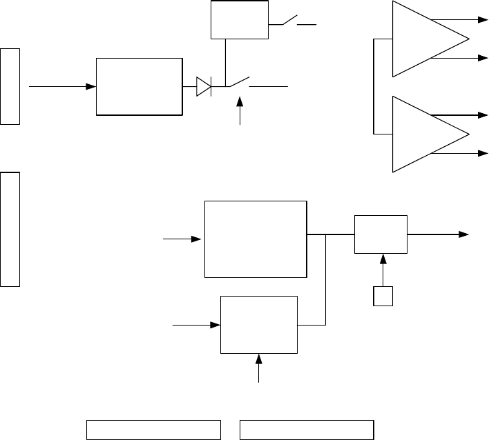
2-16 GUARDIAN VHF 110W MOBILE
2.6.6 PA ON/OFF Control (Bypass Mode)
It is possible to operate the system not utilizing the PA (PA in by pass mode.) This is done by turning on control
head on with the PTT depressed. An orange TX light indicates to the user that he is operating in by pass mode. In
this mode, output power is about 1dB lower that the nominal levels delivered from the transceiver, as indicated in
the table above. In normal mode, Q16 conducts at start-up, causing Q14 to conduct, which keeps Q15 off. When
using this mode, Q16 conducts in the reverse direction, Q14 remains off and Q15 conducts, which prevents bias
voltage from being sent to the RF power amplifier.
2.6.7 RF Power Indication
Operational amplifier U3A forces the output control voltage at Q8-E to be equal to that at U3-3. After high power
transmit is detected at the PA output. The RF PA test circuit forces additional current back into this line. The op-
amp loop holds the voltage at the input level, so the additional current is forced out Q8-C and through R44. This
forces Q9 to conduct and sink additional current from the LED_TX. The LED_TX turns off the green light. When
the unit is in bypass (low power) mode the Tx lamplights orange because the red and the green LED’s are on.
2.6.8 Audio Board Block Diagram
Audio Block diagram
RFI filter&
transient
protection
on off switch
voltage
ragulator
7.8volts 7.8volts
switched internal
audio amplifier
external
audio amplifier
audio in
power level
voltage
converter
RF&DC
combiner
RF IN
RF &control out/in
D
B
9
D
B
25
J2 - IDC 20 pin J3 - IDC 20 pin
PA on off
control
Switch PTT
7.8volts
switched
input voltage
audio out p
audio out n
audio out p
audio out n
j
4
power level input
Figure 2-4: Audio Board Block Diagram
GUARDIAN VHF 110W MOBILE 2-17
2.7 Display Board
The Display board consists of a seven-switch keypad and an LCD module with integrated LED blue backlight. The
board is heatstaked onto the plastic front panel, forming a permanent assembly. Electrical connections are made to
the Interface board via a 20-pin connector (J13).
The radio display module is a full graphics 80x32 pixels LCD, requiring a temperature compensated differential
driving voltage of about 12V and a 1/6 bias, 1/32 duty cycle driving scheme. The LCD driver device (Seiko Epson
SED 1530) drives the display. This LCD driver has an internal display RAM that copes with all the display
refreshing autonomously. Display data transfers from the main controller are only required when the display is
changed, selective display RAM updates are also available to minimize serial traffic. The LCD driver display RAM
is accessed through a one way synchronous serial interface and connected in parallel with the AVR serial port. The
LCD CS input is used to differentiate between serial data for the LCD driver and the keypad board hardware reset
line resets the display drive. The hardware is configured such that during hardware reset, before serial LCD data is
presented, the LCD is blank. The radio keypad consists of 16 keys, which contact onto switch contacts on the rear of
the keypad board.
Keypad
Figure 2-5: Keypad Board
2-18 GUARDIAN VHF 110W MOBILE
2.7.1 Control Logic Interface
The signals on this interface need not be filtered, but are protected from short circuits to ground. All logic signals
are at 0 to 3V Complimentary Metal-Oxide Semiconductor (CMOS) levels at the interface. The interface carries the
following functions:
• 10V Control
• Ground
• /RADON
• Switched 10V Supply
• Reset
• AVR Clock
• Serial Data Clock
• Serial Data Input
• Serial Data Output
• Key Interrupt
• LCD Chip Select
• LCD A0 (data\command select)
• Keypad Chip Select
2.7.2 Keypad
2.7.3 Switch Interface
Interface to switches is provided to the RECM via 80-pin connector to the Interface board.
2.8 Interface Board
This board is located in the Control Head Assembly in the vehicle cab. The transceiver (RECM) is mounted to this
board and interfaces through 80-pin connector J1. The front panel display PCA mounts to this assembly and
interfaces through 20-pin connector J4. The microphone interface is J5, an 8-pin modular connector.
Communication with the audio amplifier board and the remote RF Power Amplifier is through two 20-pin
connectors J2 and J3. The DC power for this board, the transceiver and front panel functions enters via J3. The 3.3V
powering the display and logic is generated by a linear regulator U1 powered from the 7.8V via an on/off switch
q12. All front panel switches and LED lamps are mounted to this board. Connection to the internal 5W speaker is
via J6.
ON/OFF control: Transistors Q11-14 are connected to the outputs of the binary volume switch SW3. The
transceiver uses these signals to detect the off position of the volume switch. At the off position all lines are open. If
any of the lines is switched and ignition power is high Q17 is on providing low (0V) to one of the transistor witch
will result in a positive ON/OFF voltage. This signal witch is routed also to the audio board to control power
function there and in the remote RF Power Amplifier.
SW4: Used to change channels. The transceiver uses the binary outputs to detect the position of the channel switch.
Toggle Switches: Program switch SW1 for a variety of functions. Switch SW2 is used to select between internal
and external audio speakers.
Front panel buttons: Keypad depressions on the front panel are detected by the scanning outputs from the
transceiver. Keypad depressions on the optional DTMF microphone are detected by the DTMF decoder on this
board and are processed as ordinary scan-in signals by the transceiver.
DTMF keypad processing: The optional DTMF can be used to program the radio. Keypad depressions generate a
DTMF tone in the audio output. This signal is routed to DTMF detector U6, and digital outputs are sent to1-of-16
de-multiplexer U2. The outputs from U2 are used to control analog switches U3-5. In this way the transceiver scan-
out lines can be connected to the appropriate scan-in lines to simulate a physical switch closure.
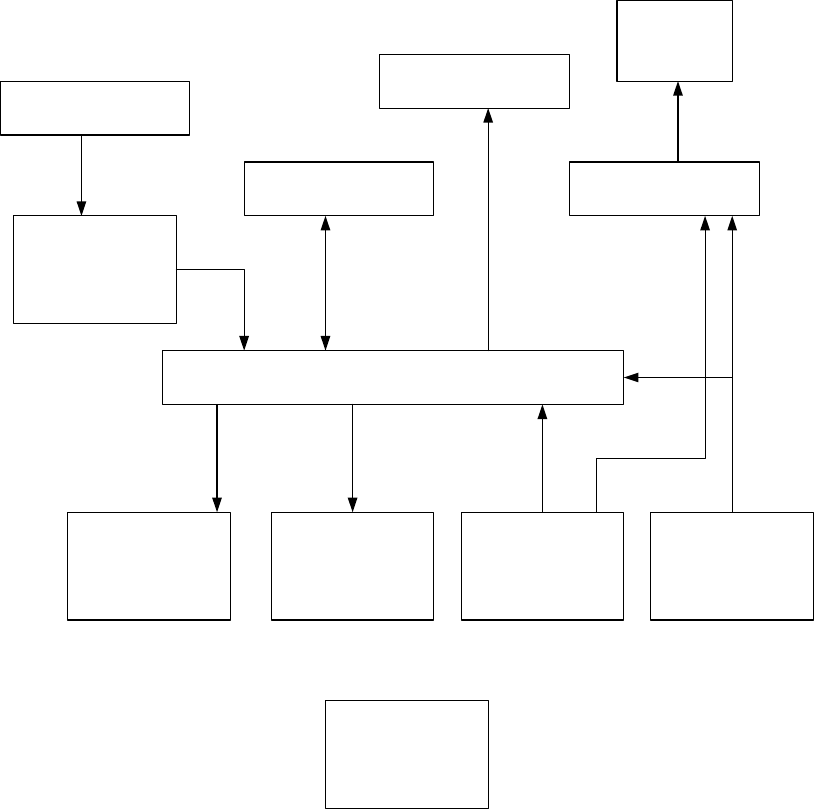
GUARDIAN VHF 110W MOBILE 2-19
PTT processing: In normal operation, a PTT switch closure causes Q2 to conduct, which in turn causes Q7 to
conduct. This signal is distributed to the rest of the radio as the PTT signal. When a DTMF button is depressed, the
transceiver automatically transmits this tone.
PTT lockout: To prevent transmission of DTMF tone during programming, a latch circuit is provided to lockout
PTT. When the ENTER button is pressed the PTT signals is disabled by a latches circuit. When the ESCAPE button
is pressed the lockout latch is reset. It is recommended to utilize the PTT condition lockout during programming the
PTT (light will stay off). This is done by pressing ENTER key and after that hold the PTT key depressed until
programming is done. To re-key the radio release PTT and key the radio once the radio is out of the programming
mode use the ESC key quit programming.
J1, 80-pin boat connection
J2, IDC, 20-pin audio
connection
J3, IDC, 20-pin audio
connection
J4, 20-pin display
connection
J5, RJ11, 8-pin MIC
and KLV connection
DTMF to keypad
interface
Programming PTT
disable
Volume selector
and on/off control
On/off controlled
3.3V regulator
LED
drivers/control
Channel, speaker
out, ABC switch
selectors
J6, 2-pin
speaker
connection
Figure 2-5: Interface Board
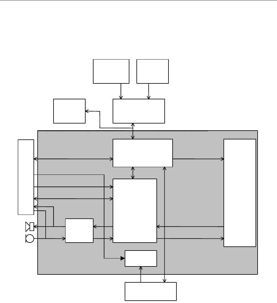
GUARDIAN VHF 110W MOBILE 3-1
CHAPTER 3: SOFTWARE THEORY OF OPERATION
3.1 Functional System Operation
3.1.1 General
All control and channel software is resident in the RECM.
3.1.2 Guardian Block Diagram
Figure 3-1: Software Theory of Operation Block Diagram
Switches
LCD
Keypad
Keypad MPU
H8 Controller
DSP
Audio
DB25 Accessory Connector
Transceiver
PSU
Power Supply
External Power
Receiver/Exciter/Control
Module (RECM)
Battery
Data
Power
Modulation
Control
IF Output
Control/Fill/Code
Keyfill
User Data

3-2 GUARDIAN VHF 110W MOBILE
3.1.3 Architecture
A single digital signal processor (DSP) handles all signal-processing functions. An H8 microcontroller is used to
control the user interface and implement other radio control functions. All references to signal names relate to the
Receiver/Exciter/Control Module (RECM). Functionality partitioning is shown in Figure 1-1.
3.1.4 Board Identification
The control logic stores an electronic serial number and modification status within nonvolatile storage on the board.
3.1.5 Self-Test on Power-Up
The software automatically executes a self-test when the radio is switched on. This test is capable of detecting and
identifying faults that prevent the radio from properly operating.
3.1.6 Flash Software Upgrades
The radio software is updated if required using a PC and the Guardian G25AXG004 PC Programming/Cloning
cable.
3.1.7 Voice Coder/Decoder (VOCODER)
The VOCODER uses an improved multi-band excitation (IMBE) voice-coding algorithm as specified in the
telecommunications industry association and electronic industries alliance (TIA/EIA)-102.BABA. The IMBE
VOCODER compresses a high-bit-rate waveform into a low-bit-rate data stream suitable for transmission over the
channel. The VOCODER operates at a net bit rate of 4.4 kbps for voice information and a gross bit rate of 7.2 kbps
after error control coding.
3.2 Radio Control Software
This software controls the transceiver and baseband signal processing functions.
3.2.1 Audio Control
H8 controls the analog audio signal processing. Audio for transmission comes via an external microphone attached
to the front panel. It is wired into the microphone amplifier, which is permanently powered.
Audio output is required when a voice message is received or a tone is generated by the user interface. To allow
audio output, H8 sets either SPKRON or EXTSPKRON to the internal speaker or the accessory connector. If an
external audio accessory is detected by who are you (WRU) <0.5 Vdc, the audio is routed to the accessory
connector. Otherwise audio is routed to the internal speaker. The 16-position volume control knob is decoded and
sent to the DSP through the controller software to control the output audio volume.
3.2.2 DSP Control Software
The DSP implements most of the baseband signal processing in the radio. Its function is controlled through its host
port by the H8 controller. The DSP operates in a number of basic modes controlled by H8 through the host port.
They are as follows:
Mode Description
Idle Current shutdown mode released through the host port
Searching Actively looking for a signal on the IF input signal
Searching paused Search algorithm paused for an economize cycle or frequency change
Active receive Actively receiving a message, initiated by detecting a signal or H8 command
Transmit Actively transmitting voice or data
Keyfill Keyfill operations and key
Management Management tasks

GUARDIAN VHF 110W MOBILE 3-3
The DSP pages-in different program images from the Flash for different modes of operation. Typically one image is
used for receive and standby modes, but a new image is needed for transmit and key management operations. The
DSP can interrupt the H8 controller, and then pass data over the host port back to H8. Interrupts from the DSP
include the following events:
• Signal detected with type data
• Signal lost
• DSP BIT errors
• Paging request
In all active modes the H8 software must be able to write a number of parameters to the DSP and also read back a
number of parameters from the DSP. This is implemented through the host port. The parameters used include:
Mode Description
Search Reference oscillator temperature used by DSP to correct frequency offsets. AGC
reset control is used at start of search period
Analog setting BW, squelch tones, squelch code, and squelch level
Digital setting Data rate, key, and algorithm
Project 25 setting NAC and TGID
CVSD setting Continuously variable slope delta (CVSD). Data rate
Receive Reference oscillator temperature used by DSP to correct frequency offsets. Audio
volume
Analog setting Squelch controls, de-emphasis, and companding
Digital setting Data rate and key algorithm
Project 25 setting NAC, TGID, BER, and test mode
CVSD setting Data rate and key
Project 25 setting Read by H8: SS bits, low-rate data (for future use), and sender ID
Transmit Reference oscillator temperature used by DSP to correct frequency offsets. Audio
volume, sidetone on/off
Analog setting Squelch controls and de-emphasis
CVSD setting Data rate and key
Project 25 setting NAC, TGID, key and low-rate data (for future use)
3.2.3 Transceiver Board
The Transceiver board is controlled through a synchronous serial bus from H8 to the transceiver allowing H8 to
control the synthesizer, two 4-channel 8-bit digital to analog converters (DAC), and a control shift register in the
transceiver board. Some of the DAC channels are set according to data in the transceiver’s electronically erasable
read-only memory (EEPROM) calibration tables.
3.2.3.1 Mode Control
The transceiver shift register and the CTX output of the field-programmable gate array (FPGA) control the modes of
operation (transmit, receive, or standby). The outputs are controlled as below:
Mode Description
Spare (SR bit 1) Spare
3.3VRXSynth (SR bit 2) Set in active receive mode, RXVCO enable
3.3VTXSynth (SR bit 3) Set in active transmit mode, TXVCO enable
3.3VRXEnable (SR bit 4) Set in active receive mode, receiver enable
Spare (SR bit 5) Spare
Spare (SR bit 6) Spare

3-4 GUARDIAN VHF 110W MOBILE
Mode Description
TX/RX (SR bit 7) Set in active transmit mode, front end TX/RX control
STD/SIDE (SR bit 8) Set to use radio antenna, reset to use accessory connector RF port
CTX (FPGA output) Set in active transmit mode to enable the RF power amplifier
3.2.3.2 Frequency Control
The frequency of operation in both transmit and receive is controlled by the H8 setting in the synthesizer through the
serial bus. To set the desired frequency, the appropriate TX or RX synthesizer enable S-R bit must be set, the serial
data loaded into the synthesizer chip, and the DAC2 output A synthesizer coarse tune set to the appropriate value for
the frequency according to the EEPROM calibration table. Synthesizer lock is monitored by the out-of-lock (OOL)
input. Once the synthesizer lock is achieved, the transmitter or receiver is enabled with the appropriate control bits
3.3VRX enable, CTX, and TX/RX. Economizing the synthesizer function is implemented by controlling the
3.3VTXS/RXS bits and by controlling the EM main divider enable bit in the synthesizer control word. If the
frequency is unchanged, the synthesizer serial data need not be reloaded when coming out of economize.
3.2.3.3 12-Bit DAC
DACLDA, DACADCCLK, and DACDOUT control the 12-bit DAC for IFAGC, TXVCOMOD, REFOSCMOD,
and VATT.
3.2.3.4 Reference Oscillator Temperature Compensation
The H8 software constantly monitors the reference oscillator crystal temperature using the XTALMON line. The
temperature data is used to lookup the compensation factor in the transceiver’s EEPROM calibration table. This
compensation factor is written into the DSP, added as a dc offset reference oscillator modulation signal, and used as
a dc offset in receive mode.
3.2.3.5 Receiver Control
Setting 3.3VRXE enables the linear receiver chain. The DSP implements software AGC system to control the gain
of the linear receiver chain. The H8 controller monitors the actual received signal level by reading RSSI. At all
times during receive the RXVTF DAC2 output C must be set to the value in the EEPROM calibration table
corresponding to the receive frequency used. This makes the receiver’s front-end tunable filter centered on the
desired frequency. At all times in receive modes the second LO DAC2 line output B must be controlled using data
from the EEPROM calibration table and indexed with oscillator temperature data XTALMON. The temperature
compensates the second LO in the receiver chain.
3.2.3.6 Transmitter Control
The radio uses a complex H8 software-based algorithm to dynamically control the transmit power of the radio. The
inputs to the power control algorithm are: requested power level (0.1W, 0.5W, 1W, 2W, or 5W), PA calibration
data in the EEPROM, supply voltage BATMON (used for monitoring), transmit frequency, PA current, (used for
monitoring), and PA temperature (used for monitoring).
The power control algorithm takes these inputs and uses them to control the following outputs to provide a steady
RF power output with a clean rise and fall at switch on/off.
Output Description
PWRSET (DAC1 output A) Sets the power level in the power amplifier ALC loop
PABIAS1 (DAC1 output B) Adjusts the bias in the final driver stage
PABIAS2 (DAC1 output C) Adjusts the bias in the final driver stage
3.2.3.7 TX/RX Switching
The procedure needed to quickly switch the transceiver from receive to transmit and back again is to shut down the
current mode, lock the synthesizer in the new mode on the new frequency, and enable the transmitter or receiver, as
required.
GUARDIAN VHF 110W MOBILE 3-5
3.2.3.8 Receiver Scanning
In some scanning modes it is necessary for the radio to scan a number of channels looking for traffic, as controlled
by the H8 software. The basic requirement is to change the synthesizer frequency, RXVTF, synthesizer tune DAC,
and to resume searching on the new frequency. The DSP may have to be informed of new traffic settings on which
to search, for each new frequency. Scanning is interrupted when the DSP detects a signal of interest.
3.2.4 DC Power Control
The H8 controller software controls the power supply switching in the radio. The control software algorithm uses
the following inputs:
Input Description
/PWROFF Indicates the current position of the radio on/off switch and the accessory connector off line
WRU Indicates if the radio is fitted into a harness providing external power
/LBOUT Indicates the supply voltage is at the minimum required for correct operation
BATBUS Not used in the mobile configuration
BATMON Indicates the voltage on the main radio supply from external power source
These inputs are used to control the following FPGA outputs:
Output Description
PWRHOLD Set during normal operation, the radio stays on regardless of the on/off switch. When
PWROFF indicates that a switch off is required, software shut down is executed followed
by a release of this output
BATOFF Not used in the mobile configuration
Additionally the /LBOUT interrupt is used to execute a fast shutdown of the software when the supply voltage drops
below that needed for normal operation, or when the power source is removed without switching the radio off.
3.2.4.1 Power Supply Frequency Control
The power supply software controls the switch mode power supply frequency output according to the RF frequency
used. The frequency is checked and changed if necessary at every synthesizer frequency change.
3.2.5 Monitoring
The H8 software monitors the following signals:
Signal Description
Out-of-lock In all active modes, every 100 ms
EPTT/RTS In all modes, every 20 ms
RSSI In receive modes, every 100 ms
WRU In all modes, every second
DC voltage In all modes, every 5 seconds
PA temp In transmit modes, every second
REF temp In all modes, every 5 seconds
PA current In transmit modes, every second
3.2.6 Radio Control Drivers
A number of low-level software drivers are used by H8, which interface to the transceiver hardware.
3-6 GUARDIAN VHF 110W MOBILE
3.2.6.1 Audio and Power Supply Unit (PSU) Driver
A serial interface driver controls the output bits of a serial-to-parallel output shift register in the FPGA. Clock and
data source for this shift register is the same serial port used for the user interface serial bus, but data is directed to
the shift register using high-order H8 address lines.
3.2.6.2 Transceiver Serial Bus Driver
A serial interface driver controls the transceiver shift register, DAC, and synthesizer. It uses a common clock and
data line, and three separate strobe lines for each device.
3.2.6.3 DSP Host Driver
The H8 software includes a DSP host driver for controlling the DSP mode of operation, and initial start-up code
download.
3.2.6.4 IIC Bus Driver
The H8 software includes a driver that allows the controller software to read and write to the transceiver EEPROM
using IIC protocols. The two lines are general-purpose I/O lines controlled on a bit-by-bit basis by the software.
3.3 Digital Signal Processing
The DSP software implements all baseband signals processing in the radio. It processes signals between the user
audio and data interface, and the transceiver modulation and intermediate frequency (IF) interfaces. The signal
processing provides compatible analog FM modes, common air interface (CAI) compatible modes, and 12 kbps
secure CVSD modes.
3.3.1 DSP Transmit Chain
Signal processing while the radio is transmitting depends on the radio's operational mode. The possible modes are
clear analog voice FM, CVSD DES voice, Project 25 clear digital voice, and Project 25 DES digital voice. The
Transmit DSP Chain block diagram is shown in Figure 3-2. The major signal processing functions of the DSP
transmit chain are described in the following paragraphs.
3.3.1.1 Audio Coder/Decoder (CODEC)
The Guardian uses a Texas Instruments® TLV320-AC36 audio CODEC. Data is transferred to and from the
CODEC using the DSP enhanced synchronous serial interface (ESSI) 0 port. The data word is 16 bits long. The
first thirteen bits are the two’s compliment audio sample, and the last 3 are the volume control word in the receive
direction (DIN), and zero padded in the transmit direction (DOUT). The DSP currently sets volume control bits for
no attenuation. Scaling the signal prior to sending it to the CODEC controls the volume. The sample rate from the
CODEC is 8 ksps.
3.3.1.2 Audio Processing Board
The Audio Processing board receives audio input from the audio CODEC, applies filtering and automatic gain
control (AGC), and transmits it to the mode-specific formatting module. The audio filter has a passband from
300 Hz to 3 kHz. This board also transmits DTMF tones to the audio CODEC. DTMF over-dial is supported to
allow redirection through the phone network via a base station. Data is transferred to and from the CODEC under
interrupt service routine (ISR) control.
3.3.1.3 Project 25 Voice Module
The Project 25 Voice module performs framing and conversion tasks. The framing function uses its own task table
to build a CAI time-division multiple access (TDMA) frame. This includes compression of the voice signal using
the IMBE VOCODER, forward error correction, and encryption. The physical layer task converts a 4.8 ksps dibit
data stream into a 48 ksps real sampled waveform, which is then fed to the Modulation module. The physical layer
scales each dibit symbol so that the proper frequency deviation is attained. It applies raised cosine filtering for
control of inter-symbol interference.
GUARDIAN VHF 110W MOBILE 3-7
Figure 3-2: Transmit DSP Chain
3.3.1.4 CVSD DES Module
Audio data from the Audio Processing module is sent to the audio circular buffer. The sample rate is increased from
8 ksps to 12 ksps. The CVSD encodes the data and sends it to the transmit CVSD audio circular buffer. The data is
DES-encrypted and differentially encoded before sent to the physical interface buffer. The CVSD physical layer
converts the CVSD encoded, DES encrypted 12 ksps data stream into a 48 ksps waveform suitable for processing by
the Modulation module. The module contains a finite impulse response (FIR) raised cosine filter that acts as an
interpolation filter. Transmitting an end of message (EOM) indicator, consisting of 160 ms of alternating ones and
zeros, signals the end of a transmission. This allows the receiving radio to squelch the audio output before the radio
stops transmitting.
3.3.1.5 Analog FM Module
Audio data entering the Analog FM module is sent through a linear-phase, FIR, audio-shaping filter. Interpolation
from 8 ksps to 48 ksps is accomplished using a linear-phase, FIR filter. A single-quadrant sine look-up table (LUT),
using fractional addressing and quadrant folding, generates continuous tone controlled squelch system (CTCSS)
tones. If the DCS audio turn-off code is transmitted, the tone is fixed at 134.4 Hz and the codes transmitted at a rate
of 134.4 bps, derived using the CTCSS tone generator. The DCS data stream passes through a raised cosine filter
before added to the speech. The 8 ksps audio stream, with CTCSS/DCS controls, is interpolated to 48 ksps before
sent to the Modulation module.
3.3.1.6 Modulation Module
The Modulation module prepares the signal for transmission. The signal is split into a reference oscillator signal and
a voltage controlled oscillator (VCO) signal. This allows independent scale and offset values for each signal. A
modulation-balance variable scales the reference oscillator voltage, so that the maximum frequency deviation is
constant for all RF channels. A transmit modulation variable does the same for the VCO signal.
CVSD DES
Module
Audio
CODEC
Transceive
r
Audio
Processing
Module
Modulation
Module
Project 25 Voice
Module
Analog FM
Module
VOICE
DTMF
Tones
3-8 GUARDIAN VHF 110W MOBILE
3.3.1.7 Transceiver Interface
The transceiver DAC has four output ports, two of which modulate the carrier. One of the two channels maintains
carrier frequency accuracy. On transmit channel changes, the controller provides the DSP with two fractional values
used to scale the two signals output from the DAC. The controller provides the DSP with an additional integer value
at one second intervals, and is added to one of the DAC output signals to control carrier frequency accuracy. The
modulation interface receives modulation data samples at 48 ksps, independent of the transmit mode. When the
radio is operating as a transmitter, the transceiver interface controls the operation of the DAC via ESSI 1 on the
DSP. Data is written to the DAC at 96 ksps.
3.3.2 DSP Receive Chain
The radio receive chain hardware consists of an RF transceiver board, analog to digital converter (ADC), a
Motorola® DSP 56302 or DSP 56309, and an audio CODEC. The Receive DSP Chain block diagram is shown in
Figure 1-3. The major signal receive functions of the DSP receive chain are described in the following paragraphs.
Figure 3-3: Receive DSP Chain
3.3.2.1 Transceiver
The RF transceiver board performs mixing and filtering of the received signal to produce a 455 kHz, 25 kHz
bandwidth (BW), IF signal. The output signal from the transceiver is digitized by the ADC and fed to the DSP. The
bulk of signal processing is performed by the DSP. An ISR that implements the transceiver/ADC/DAC interface is
called at a rate of 96 kHz in receive modes. The ISR reads ADC output data, stores the values in a circular buffer,
and controls data transmission to the DAC.
3.3.2.2 FM Demodulator
The FM demodulator converts the FM output of the transceiver to a real-valued, baseband signal. FM demodulation
is implemented by a discriminator task. Sub-sampling the 455 kHz IF at 96 kHz folds down the signal to 25 kHz. A
mixing function mixes the sampled IF data in the input buffer before filtering. For 12.5 kHz channels, a second
CVSD DES
Module
Audio
CODEC
Transceiver
Audio
Processing
Module
FM
Demodulator
Project 25
Voice Module
Analog FM
Module
Signal
Detectors
GUARDIAN VHF 110W MOBILE 3-9
filter is applied to the IQ data stream. Calculating the angular difference between consecutive IQ pairs demodulates
the received signal.
3.3.2.2.1 Analog to Digital Converter
Because the signal BW is much less than the 455 kHz carrier frequency, the ADC sub-samples the 455 kHz IF
producing a frequency translation as part of the sampling process. The ADC sampling rate is 96 ksps.
3.3.2.2.2 25 kHz Frequency Translation
The 25 kHz frequency translation converts the signal image into a baseband signal, centered at 0 Hz. The DSP
implements the digital equivalent of a mixer to perform frequency translation.
3.3.2.2.3 IF Filtering
The complex baseband signal is sent through two linear phase FIR filters. The first IF filter is used as a decimate by
two, polyphase, FIR filters and applied to the 96 ksps, complex, baseband output of the 25 kHz mixer. This filter
removes some of the out-of-band noise produced by the nonlinear analog components of the transceiver. CVSD
DES and analog wide modes have a 25 kHz BW and the first IF filter is the only filtering performed for these
modes. Project 25 and analog narrow modes have a 12.5 kHz BW. The second IF filter provides the filtering
required for these modes and is applied to the 48 ksps output of the first IF filter.
3.3.2.3 Signal Detectors
The radio uses three signal detectors to detect the presence or absence of a modulated signal in the tuned channel.
These signal detectors search for Project 25, analog FM (including noise, CTCSS, and DCS), and CVSD DES
signals.
3.3.2.3.1 Project 25 Detector
The Project 25 frame detector detects a Project 25 signal by searching for the frame synchronization (FS) signal and
network identifier (NID) embedded in the preamble of every Project 25 data unit. The detector uses this information
to perform bit recovery and packet identification. It processes and buffers the binary data for use by the Project 25
Voice Module. Once a target signal is detected, the radio disables squelch using an enable transmit function, so the
user can monitor the signal. If the detected signal is lost, squelch is enabled by the shutdown active receive
function.
3.3.2.3.2 Analog FM Detector
The analog FM detector uses a function to decimate the incoming data stream by six, to run the noise detector,
CTCSS single-tone detector, CTCSS multi-tone detector, and the DCS multi-code detector. A noise squelch detect
function detects the appearance of a carrier by searching for a drop in power in a frequency band just above the
audio band. In the analog noise detector, the input data is scaled and high-pass filtered, then rectified and scaled
again. Then the data is low-pass filtered. The output of the low-pass filter is used to determine whether or not a
signal is present.
The detector has two states, searching and locked. If the detector state is searching and the detected power drops
below the lower squelch threshold, the detector state transitions to locked. Conversely, if the detector state is locked
and the detected power rises above the upper squelch threshold, the detector state transitions to searching. Upper
and lower threshold values are BW dependent and can be adjusted at run time.
The multiple-value DCS detector searches for a 134.4 bps bit stream in the sub-audible frequency band used for
DCS codes. If found, the code is extracted and appropriate state variables updated. Code extraction is performed in
two steps: input data is converted to a binary bit stream, and then data extraction and code comparisons are
performed.
The conversion of the input data to a binary bit stream starts with the 8 ksps input data sent through a decimate by
six, FIR filter to produce a 1.33 ksps, real valued data stream. This filter removes any signal energy outside of the
sub-audible frequency band. The data is then split into two paths. The lower path estimates the dc content of the
signal with a narrow low-pass infinite impulse response (IIR) filter. Subtracting the lower path signal from the
3-10 GUARDIAN VHF 110W MOBILE
upper path signal removes the dc component from the upper path signal. Following this, the resulting signal passes
through a single-bit quantizer and the output buffered for use by the code removal step. Data extraction and DCS
code comparisons are then accomplished.
3.3.2.3.3 CVSD DES Detection
Detection of CVSD DES waveform is performed by a secure detection function. This function also recovers the
12 kbps bit stream from the 48 ksps input signal. The detector looks for a 12 kbps data stream to determine if a
CVSD signal is received.
3.3.2.4 Project 25 Voice Module
The physical layer task extracts FS, NID, SS symbols, and data. All other dibits are passed to the receive framing
task. The module performs recovery and symbol extraction based on frame synchronization using a correlation
detector. Symbol extraction and error-correction decoding follow carrier frequency offset compensation.
VOCODER data and Project 25 framing data is removed and secure mode decryption performed. The VOCODER
converts the compressed voice data stream to a 8 ksps audio data stream that is sent to the Modulation module.
3.3.2.5 Analog FM Module
The analog FM module performs two tasks. The detection task uses an FIR filter to down-sample the FM
demodulated bit stream from 48 ksps to 8 ksps. It then uses four detectors (noise, single-tone CTCSS, multi-tone
CTCSS, and multi-code DCS) to determine signal squelch. The post-detection audio-shaping task applies de-
emphasis on/off filtering to a received clear analog signal.
3.3.2.6 CVSD DES Module
The CVSD DES module consists of a 12 kbps clock detection/recovery task, a 12 kbps symbol resolver, a
differential decoder, a DES decoder, a 12 kbps CVSD decoder, and a 12 ksps to 8 ksps sample rate converter. The
input to the clock detection algorithm is a 48 ksps data stream, representing the sampled FM demodulated carrier.
To allow for variation in carrier frequency, the dc component of the demodulated carrier is removed before zero-
crossing detection. From a zero-crossing phase profile, a decision can be made whether a 12 ksps data stream is
present on the demodulated carrier, or a 12 kHz clock recovered for usage within the 12 kbps symbol resolver.
Differential encoding of the binary FSK modulation ensures compatibility between manufacturers, so that either a
positive or negative frequency shift can be used to represent a 1 symbol. In the CVSD receive chain, differential
decoding precedes one-bit cipher feedback DES decoding. To conserve memory and aid processing efficiency, all
symbols (encoded and decoded) are packed in memory. The 12 kbps CVSD decoder is modeled after FED-STD-
1023.
The decoder consists of a modulation level analyzer (MLA), a syllabic filter, a pulse modulator, a principal
integrator and a comparator. The output of the CVSD decoder is at 12 kbps and must be changed to 8 ksps for
output by the CODEC.
3.3.2.7 Audio Processing Module
An audio receive task function and an audio filter is used to output Project 25, clear analog, or secure analog speech
samples to the CODEC. When in active receive modes, the ISR is enabled and the task outputs data to the CODEC
circular buffer as data is written to it’s audio input circular buffer.
3.3.2.8 Audio CODEC
The audio CODEC and the DSP interface uses the DSP ESSI 0 port. The serial clock to the CODEC operates at
2.048 MHz, and is derived from the DSP internal clock. ESSI 0 is configured to operate using a frame rate divider
of 16 and a word length of 16 bits, transmitting packets of encoded audio to the CODEC at 8 kHz. The CODEC is
used in a linear decode mode, where 13 bits are used to represent the full audio range. The post-processed DSP
signal is fed to the audio CODEC, which converts the signal to an analog waveform, applies gain, and routes it to
the appropriate output device.
GUARDIAN VHF 110W MOBILE 3-11
3.3.3 DSP Software
The program data for the DSP is stored in 64K Flash program blocks. The data is stored as unpacked bytes. The
blocks used for the DSP software are dedicated so that selective upgrades of this code only are possible.
3.4 Keypad MPU Software
3.4.1 Overview
The keypad microprocessor unit (MPU) provides an indirect interface via the Motherboard to the DTMF keypad and
front panel switches. It communicates with the main controller via a synchronous bi-directional serial link.
3.4.2 General
The software is designed so that processor activity and current consumption is minimized. The only continuous
operation required is keypad scanning and switch reading. An external clock at 1.5 MHz clocks the keypad. The
hardware reset is supplied from the main controller.
3.4.3 Keypad Scanning
The keypad scanning software continuously scans the keypad at a rate of a row every 10 ms. A debounce period of
40 ms is used on key presses and key releases. The software deals with simultaneous key presses and key rollovers,
making only single key presses valid. Debounced and validated key presses are passed to the serial data output
buffer.
3.4.4 Push-to-Talk (PTT) Input
Inputs from the momentary input switches, and the PTT and auxiliary keys, are read every 10 ms and are debounced
for 40 ms. The validation software filters out simultaneous presses of the auxiliary keys and the key rollover
between them. Simultaneous presses of the PTT switch and one auxiliary key are allowed. Debounced and
validated auxiliary key presses and PTT press and releases are passed to the serial data output buffer.
3.4.5 Switch Input
Inputs from the rotary switches and toggle switch are read at least every 40 ms. Changes in state are debounced for
100 ms. Debounced new switch positions are passed to the serial output buffer.
3.4.6 LED Output
The outputs to the LED are controlled under instruction from the serial port. It is possible to set both outputs off, set
the red LED on, set the green LED on, set both LEDs on (orange), and to flash either or both on a 50% duty cycle at
a controlled rate of approximately 1 Hz.
3.4.7 Backlight Control
The two LCD backlight controls for setting bright and dim operations are controlled under instruction from the serial
port. The keypad uses a fixed level backlight operation. A timeout facility switches off the backlight after
30 seconds if not requested by the main controller.
3.4.8 Serial Interface
The keypad controller implements a synchronous bi-directional serial interface using its serial port allowing it to
interface to the main controller. The main controller always sources the serial data clock. To allow autonomous
transfers from the keypad controller, a separate keypad interrupt line is provided with the interface. The interrupt
line is used to request 8 clocks from the main controller to transfer data from the keypad. The LCD chip select (CS)
input line is used to distinguish between serial data for the keypad controller and LCD driver. The serial interface
supports the following transfers:
• Keypad to controller including:
3-12 GUARDIAN VHF 110W MOBILE
Keypad power up okay
Keypad error 1-n
Key press 1-16
Key release 1-16
PTT press
PTT release
Volume switch 1-16
Channel switch 1-16
Toggle switch 1-3
Auxiliary key press 1-3
Emergency key press
• Controller to keypad
• Request current switch status
• Reset and execute BIT test
• Backlight off/bright/dim
• LED off/red/green/yellow/flash/flash rate
• Key press request and interrupt acknowledge
LCD data transfers are in blocks of 80 bytes maximum, allowing a pause on the serial interface at least every 100 ms
for the keypad MPU to assert the interrupt and transfer key press or switch change data. During the LCD data
transfers, the key data are buffered into the keypad MPU.
3.5 Data Interface
The DSP incorporates a user data interface through its SCI port.
3.5.1 CAI Data Interface
The DSP supports an asynchronous data interface for CAI modes using its SCI port. This interface conforms to the
CAI data peripheral interface. It uses standard V24, and RS232 baud rates up to 9600 baud. The software also
controls the associated flow control signal data of the terminal ready (DTR) input to the DSP, and the clear to send
(CTS) output from the DSP. The request to send (RTS) input to the radio for this interface is processed by H8.
3.5.2 Synchronous Serial Data Interface
The DSP supports a 12 kbps synchronous serial port using its SCI port. The interface is half duplex, uses a DSP
generated clock, and includes minimum data buffering within the DSP and RTS/CTS flow control on the transmit
function.
3.5.2.1 Receiver Synchronous Serial Data Buffering
In receive synchronous serial data modes the DSP software uses a variable length first-in first-out (FIFO) buffer to
cope with differences in clock rates between the transmitter and receiver.
3.5.3 CAI Data Link Layer
This software provides the link between the raw voice and data bit streams, in addition to the data formats required
to implement a 9.6 kbps CAI compatible interface.
3.5.3.1 CAI Transmit Voice Mode
The DSP software takes the 144 bit voice code words (encrypted or not) and a number of link control fields set by
the host H8 or from the DES system, and formats CAI-compatible logic link data units.
3.5.3.2 CAI Transmit Voice Test Modes
The DSP software is capable of transmitting the CAI voice silence test pattern, the CAI 1 kHz test pattern and a
9 x 144-bit (1296) PRBS test pattern used for error rate tests. The H8 controller controls these test modes.
GUARDIAN VHF 110W MOBILE 3-13
3.5.3.3 CAI Receive Voice Mode
The DSP takes the 9.6 kbps CAI-compatible data stream and framing, and splits out the voice data for passing to the
VOCODER. The DSP decodes the link control words so that the host H8 can read the link control fields, and the
encryption synchronization information is available to the encryption process. CAI receive processing is initiated by
the frame synchronization correlator trigger. When this is asserted the next 64 bits of network identifier (NID) data
are decoded and checked. If the NAC code matches the one selected for the channel, voice or data processing
proceeds, otherwise the physical layer is forced into search mode.
3.5.3.4 CAI Receive Voice Test Mode
The DSP software is capable of testing the 9 voice code words received in a CAI frame against a known 9 x 144
PRBS segment. The total number of errors in that frame is then output to the H8 controller. The H8 controller
controls this test mode.
3.5.3.5 CAI Transmit Data Mode
The DSP selects the user data (encrypted or clear) and a number of link control fields set by the host H8 or from the
DES system, and formats logic link data units compatible with the CAI at 9600 bps.
3.5.3.6 CAI Receive Data Mode
The DSP selects the 9.6 kbps CAI-compatible data stream and framing, and splits out and decodes the data for
passing to the user data port. The DSP decodes the link control words so that the host H8 can read the link control
fields, and the encryption synchronization information is available to the encryption process.
3.5.4 Transmit Physical Link Layer
This software uses common modulator interface software and a number of mode-dependent, physical link layer
software modules.
3.5.4.1 Transmit Modulation Interface
The software provides a common interface to the dual modulation, DAC in the transceiver through its SSI serial port
1 for all transmit modes. In transmit modes, the SSI uses an externally sourced clock at 3072 kHz. This interface
takes frequency deviation samples at 48 kHz, and writes each value scaled by a fixed number set by the host to both
the reference oscillator DAC and the VCO DAC. Additionally a host-controlled dc offset is added to the reference
oscillator DAC value.
3.5.4.2 Transmit CAI Physical Link Layer
This software takes the 9.6 kbps CAI-compatible data stream and converts it to 48k samples of frequency deviation
data. To achieve this the software implements the dibit for symbol mapping, Nyquist, and shaping filters as
described in the CAI.
3.5.4.3 Transmit Analog FM Physical Link Layer
This software takes the 8 ksps filtered audio and converts it to 48 ksps of frequency deviation data compatible with
TIA/EIA-603 in 12.5 kHz and 25 kHz modes. The signal processing uses additional high-pass filtering to reduce the
energy in the DCS tone band, audio band pre-emphasis if required, DCS tone addition, and deviation limiting and
smoothing. The software is capable of operation in 12.5 kHz, and 25 kHz channel spacing with appropriate
deviation scaling. It is capable of appending a phase reversed tone burst of 180 ms as defined in EIA-603,
generating DCS and audio turn-off codes, and companding the voice signal in 12.5 kHz mode.
3.5.4.4 Transmit CVSD Physical Link Layer
The transmit CVSD physical link layer converts the 12/16 kbps CVSD data stream and converts it to 48 ksps of
frequency deviation data. The software implements a pre-modulation filter with raised cosine time response and
100% eye height.
3-14 GUARDIAN VHF 110W MOBILE
3.5.5 Receive Physical Link Layer
This software uses common FM demodulation software, and mode-dependent receiver physical layer software
modules.
3.5.5.1 Receive ADC and DAC Interface
In receive modes SSI port 1 is used in a duplex manner to allow the ADC to be read continuously at 96 kHz and the
DAC written up to 48 ksps for AGC and reference oscillator adjustment. In receive modes, the SSI port is clocked
at 1536 kHz from an external clock source, using a 16-bit cycle. At every cycle a value is read out of the ADC. At
every other cycle a value may be written to one of the DAC channels to control the AGC and reference oscillator.
3.5.5.2 FM Demodulator
This software provides a common interface to the 96 ksps IF signal at SSI port 1 and produces 48 ksps of frequency
deviation data for use in all modes. The SSI port uses an external clock at 1536 kHz. The software implements an
FM demodulator function using a quadrature mix with a 24 kHz (Fs/4) local oscillator, dual I and Q channel filters,
and a frequency estimator. The channel filtering function is programmable-dependent on the channel spacing used.
The channel filtering provides the adjacent channel filtering in addition to that provided by the hardware to achieve
the radio adjacent channel rejection performance.
3.5.5.3 Receive CAI Physical Link Layer
This software takes the 48 ksps of frequency deviation data and outputs a 9.6 kbps data stream. The software
implements an integrate and dump filter and data slicer as described in the CAI. The integrate and dump filter is
controlled by a clock recovery function that selects one of ten possible phases for output to the slicer. The slicer
incorporates an averager with a time constant of at least 100 bits, to correct for dc offsets in the received signal.
In parallel with the above, a FIR correlator searching for the CAI fixed framing sequence of 24 symbols operates on
the filtered 48 ksps of frequency deviation data. The correlator operates at 10 samples per symbol. The correlator
phase with the highest correlation peak selects the clock phase for use in the integrate and dump filter and slicer.
This correlator operates continuously when searching for CAI traffic and occasionally when tracking an CAI signal
when subsequent frame syncs are expected. The correlator trigger is used to provide a framing signal for the
subsequent CAI link layer processing.
3.5.5.4 Receive Analog FM Physical Link Layer
This software takes the 48 ksps frequency deviation data and outputs 8 ksps of audio to the receive audio processing.
Software signal processing implements a high-pass filter to remove CTCSS tones and de-emphasis if required. The
gain of the signal path is adjusted to cope with the different deviations used on different channel bandwidths. The
signal processing signal path is controlled by squelch signals. The software includes audio expanding to reverse the
transmit companding.
3.5.5.5 Receive CVSD Physical Link Layer
This software takes the 48 ksps frequency deviation data and outputs 12/16 kbps serial data. The software uses a
data filter, a slicer, and a clock recovery function.
3.5.6 DES Encryption
The DSP software implements DES encryption of traffic in the CAI and CVSD modes.
3.5.6.1 DES Kernel
The DSP software implements the DES encryption kernel as described in FIPS 46-2, encrypting 64 data bits using a
56-bit key. It uses output feedback operation or a single bit cipher feedback operation.
GUARDIAN VHF 110W MOBILE 3-15
3.5.6.2 CAI Encryption
The DSP software uses DES kernel software to implement the CAI encryption of voice traffic as described in
TIA/EIA/IS-102.AAAA. The key manager supplies the encryption key. In transmit, the message indicator (MI)
vector is passed to data link processing for encoding and transmission. In receive, the data link layer decodes the MI
vector, and fly wheeled if decoding fails for up to n frames.
3.5.6.3 DES Data Link Layer
This software encrypts and decrypts the 12 kb of CVSD data using the DES kernel. During transmit, framing
synchronization data and the MI vector are inserted into the data stream. In receive, the software searches for and
extracts the framing and MI data. Bit definitions and formats are defined in the DES protocol.
3.5.6.4 Key Interface
This software provides an interface for inputting DES encryption keys from the DSP SCI port using synchronous
data transfers with an external clock, and for conforming to the Motorola KVL data transfer mechanism and the CAI
DES keyfill protocol.
3.5.6.5 Key Bank
The radio maintains a bank of up to 16 encryption keys stored in Flash memory. Associated with each key are a key
ID, key data, and an 8-character alphanumeric tag. Each encrypted channel is assigned one of the 16 keys for both
secure transmit and secure receive modes. Channel key assignment is accomplished by selecting the corresponding
key tag. Upon entering the secure transmit or secure receive mode, H8 transfers the appropriate encryption key to
the DSP through the SCI port.
3.5.7 Host Interface
The DSP is controlled through its host interface by H8. It initially boots up through this interface. The host
interface is used for DSP mode control, encryption key transfer, link control data transfer, low-rate data transfer,
frequency variable data transfer, CTCSS mode control, and initial software download.
3.5.8 Flash Interface
The DSP has direct access to the main radio Flash memory through the H8 bus arbitration logic. This interface is
used for software downloads using byte-wide direct memory access (DMA) transfers under host control for mode
changes. The DSP software does not write to Flash memory.
3.5.9 Paging
The DSP software is designed so that normal operation does not involve off-chip bus accesses. This means the code
size must be limited to 24K words and the data memory to 10K words. A number of program images that
correspond to different modes are allowed, with paging of images out of Flash by the DMA at mode changes. The
minimum subdivision of images corresponds to the following modes, and a continuously resident core host interface
function.
• Initialization/POST
• Receive 12.5 kHz
• Receive 25 kHz
• Transmit 12.5 kHz
• Transmit 25 kHz
• Keyfill
The paging DMA mechanism is controlled by the host H8 and allows the transfer of a program image within 50 ms.
3-16 GUARDIAN VHF 110W MOBILE
3.5.10 Hardware Control
The DSP software controls the DSP clock rate through the phased locked loop (PLL) output divider. The DSP clock
rate is dynamically matched to the mode of operation, in coarse steps for example, between searching and tracking
receive modes. The DSP software uses low-current wait modes in pauses between processing to minimize current
consumption. The host is also able to request a very low-current idle mode in the DSP. The host releases this mode.
3.6 Controller Software
3.6.1 Overview
The controller software has overall control of the radio; including user interface operations, and the DSP and
transceiver. Figure 1-4 is the controller software block diagram.
Figure 3-4: Controller Software
3.6.2 Environment
3.6.2.1 General
The H8 controller system is designed for minimum external bus activity and minimum current consumption. These
features are provided by the maximum use of low-current standby modes in H8, and an interrupt-driven architecture,
with a minimum of input polling. In radio standby and receive modes the only H8 tasks are the control of the
transceiver frequency and DSP mode as the radio scans and economizes. The most H8-intensive activities are
associated with user interactions, and operations on the fill/program/control port.
3.6.2.2 Scheduler
H8 operates with a simple scheduler that launches tasks after interrupt events. A time base interrupt of 10 ms is
used to keep track of time and poll inputs at regular intervals.
Radio Store
MMI Software
MMI Drivers (AVR)
Alarms Switches
and Keys LCD
Ke
y
Fill Data
Radio Control Software
Audio BIT
Monitor
EEPROM DSP
PSU
Control Battery
Power/Mode
Control
Frequency
Control
Transceiver
Driver
Audio/PSU
Driver
DSP
Host
IIC Bus
Driver
BATBUS
Driver
Fill/Program/
Control
Software
PC
Serial
Port
Drive
r
Environment
Software
Main
Controller/
Schedule
r
Debug
Serial
Driver
FPGA
Configure
Driver
Software Update
Drive
r
Radio
State

GUARDIAN VHF 110W MOBILE 3-17
3.6.2.2.1 Interrupt Sources
The following interrupt sources are used in H8.
Interrupt Source Description
User interface External interrupt from the keypad
DSP External interrupt from the DSP, signal detected, etc.
Low dc voltage External NMI from power supply indicates power supply fail
Timer Internal time base tick interrupt every 10 ms
PC serial port Internal interrupt from PC interrupt serial port
UI serial port Internal interrupt from user interface serial port, key press, and LCD data
Debug serial port Internal interrupt from DMA/timer
Alarm generator Internal interrupt from DMA/timer
3.6.2.2.2 Polled Inputs
The H8 software polls the following inputs at regular intervals.
Input Description
EXTPTT/RTS External PTT and data RTS
OOL Synthesizer out of lock
PWROFF On/off switch position
SENSE External keyfill device detect
The following analog inputs are measured as appropriate to the radio mode of operation.
Input Description
RSSI Receiver signal strength
WRU External device detect
BATT Main radio 10V supply monitor
PA TEMP Transmitter temperature
XTAL TEMP Reference crystal temperature
PA CURRENT Transmitter current
3.6.2.2.3 Watchdog
A regular watchdog service task is scheduled to prevent the H8 watchdog controller from overrunning, and a
hardware reset from occurring. The target watchdog timeout is 100/200 ms.
3.6.2.3 Start-Up Software
3.6.2.3.1 Boot Block Start-Up Software
The minimum simplest start-up software is provided in the boot block of the Flash. This software holds the keypad,
DSP, user interface, and FPGA in reset, and then establishes whether a valid H8 program image exists in the
program blocks of the Flash. If no valid program exists, a simple alarm sounds. The boot block software includes a
minimum basic BIT facility to check the code itself, and the internal and external random access memory (RAM).
The boot block code includes the software to allow programming of the program blocks through the PC serial port.
3-18 GUARDIAN VHF 110W MOBILE
3.6.2.3.2 Full Start-Up Software
If a valid H8 program image exists, the full start-up code executes. This involves initializing RAM, DSP, keypad,
user interface, FPGA, transceiver, etc., executing the start-up BIT, and transferring control to the main scheduler.
3.6.2.3.3 FPGA Configure Software
At start-up H8 configures the FPGA using data from the main Flash memory and transferring it via a synchronous
serial bus to the FPGA.
3.6.2.4 Shut Down Software
At normal shut down when the front panel on/off switch is off, the H8 software executes a clean shut down to the
transceiver, DSP, and user interface (UI), saves any usage data to the Flash, and releases the main power supply. In
cases where the power is removed, the low-power interrupt executes a minimum fast shut down, saving RAM data
as required, with no Flash update.
3.6.2.5 Debug Driver Software
The H8 controller includes software to implement an asynchronous serial port on two input/output (I/O) pins of H8.
Facilities provided include the ability to monitor particular radio variables, and to control specific variables. This
port allows PC serial access to the board during board-level factory testing, through the test connector.
3.6.3 Radio Store
All functional areas of the controller software, including the user interface, access the radio data store, fill control,
and radio software.
3.6.3.1 Physical Data Storage
The radio data is physically stored in 4 devices, all devices are accessible by the controller software.
3.6.3.1.1 H8 Internal RAM
The H8 controller has 2K x 8 of internal RAM. This data is not retained when the radio is switched off or the power
is removed. It is used for short-term storage of frequently accessed variables, stack workspace, etc. to minimize bus
activity when the H8 controller is running. The internal RAM is used as program space from which to execute
during some Flash update operations.
3.6.3.1.2 External RAM
H8 is provided with an external 128k x 8 bit RAM that is backed up for at least 30 seconds when the radio power is
removed, and at all times when a external power is applied with the radio switched off. This device is used as a
variable data expansion area, and stores specific user-entered data that must be retained over power interruptions
(unlock password, etc.).
3.6.3.1.3 Flash ROM
H8 has a 512k x 16-bit Flash read-only memory (ROM) used primarily for program storage. Data in the Flash is
retained permanently. Different areas of the Flash have different characteristics. The boot sector is a 16k block
used for the reprogramming software and the radio serial number. The data in this sector is programmed or block-
erased only in the factory.
The Flash has 15-64k and 6-8k program blocks that can be block-erased and programmed by the boot block code
during normal reprogramming operations, without special equipment and without opening the radio. These blocks
are used for H8 and DSP operating software, radio fill data, and FPGA programming data. The Flash has two small
8k parameter blocks used for changing data that must be stored indefinitely, such as user specific settings and usage
data.
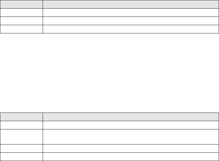
GUARDIAN VHF 110W MOBILE 3-19
3.6.3.1.4 Transceiver EEPROM
The radio transceiver has an 8k x 8 serial EEPROM for storing transceiver calibration data. This data is set during
production testing for the specific transceiver. The data in this device is essentially constant and is never written to
by the main controller. At switch on, contents of the EEPROM are copied into the external RAM; EEPROM is not
accessed during normal operation.
3.6.3.2 Data Types
The controller software uses a number of different data types.
3.6.3.2.1 Volatile Variables
Variable data used by the H8 controller that is not retained when the radio is switched off, is stored in the H8
internal RAM and the external RAM.
3.6.3.2.2 Short Term Stored Variables
Variable data retained while the radio is switched off or the power is interrupted, is stored in the external RAM.
3.6.3.2.3 Permanent Stored Variables
Variable data retained indefinitely is stored in the parameter blocks of the Flash. Every time this data changes, a
parameter block must be erased, and the new data written into the now blank parameter block.
3.6.3.2.4 Radio Fill Data
The frequencies, modes, and power levels are associated with different channels programmed into the radio. This
data is programmed into the radio through the fill port.
3.6.4 Program/Fill/Control Interface
The controller provides a serial port for PC access to allow the following functions:
Function Description
Programming To update radio software
Filling For modifying the radio data store of modes and frequencies, etc.
Control For controlling the radio operating mode
3.6.4.1 Radio Programming
The controller software allows reprogramming of the Flash memory program blocks, on a block-by-block basis.
During these operations, the controller executes from the boot sector of the Flash and no radio or user interface
operations are possible. After a programming operation, cycle the power on the radio. Programming operations are
initiated on receipt of a specific serial message on the PC serial port.
3.6.4.2 Radio Fill
The controller provides the facilities to modify the system, group, bank, and radio global data through the PC serial
port. This interface provides the following facilities:
Facility Description
Radio erase Delete all fill data in the radio
Selective erase Delete (mark as deleted) specific systems, groups, and banks (for
future use)
Radio fill Add specific systems, groups, banks, and global data to the radio store
Radio read Export the fill data contents of the radio store to the PC

3-20 GUARDIAN VHF 110W MOBILE
All transfers and operations on the fill port are cyclic redundancy checked (CRC) and acknowledged.
3.6.4.2.1 Cloning
The radio can export channel data to other radios. Data export is initiated by a user interface operation at the
exporting radio. The exporting radio emulates a PC programmer during the data transfer. Cloning of keyfill data
is not allowed.
3.6.4.2.2 Radio Keyfill
The DSP software manages the radio keyfill protocols.
3.6.4.3 Radio Control Port
It is possible for an external PC to control the functioning of the radio. This provides the following facilities:
• Radio status read to export the radio serial number, revision status, history, usage, etc.
• Set external control mode
• Set radio transmit frequency, power level, and mode
• Set radio receive frequency and mode
The transceiver mode control also allows transmission of 1 kHz test tones in analog modes, and BER test patterns in
digital modes. The receiver mode control allows the continuous (every 0.5 second) output of the bit error count per
frame in digital modes.
3.6.4.4 PC Serial Port Driver
The controller software controls the H8 serial port to implement the asynchronous data formats and baud rates
(9,600, 19,200, and 38,400) for the PC serial port. The serial port driver software also controls the 232OFF signal to
maintain the RS232 in its low-current standby state, except when data is driven out and while RTS is asserted.
3.7 User Interface
The radio interface is described in the following paragraphs.
3.7.1 Display
The radio has an 80 x 32 dot matrix LCD display. Some of the features of the display are:
Feature Description
Phone Indicated by an icon in the top, right of the display (for future use)
Scan Indicated by SCAN****, SRCH****, or ZONE**** flashing in the top row of the display
Encryption Indicated by a key icon
Power level Indicated by HI/LO/2W in the bottom row of the display
Priority scan Indicated by SCANP1 (P2), SRCHP1 (P2), or ZONEP1 (P2) flashing in the top row of the
display
Receive only channel Indicated by an RX in the bottom, left corner of the display
Talkaround Indicated by a TA in the bottom, left corner of the display
Repeater mode Indicated by a receiver icon in the bottom, left corner of the display
Emergency message EMG displays in the bottom, left corner when the radio is transmitting an emergency
message
3.7.2 Optional DTMF Microphone
The radio is programmed using DTMF microphone. For detailed instructions on programming the radio a DTMF
microphone, see the Guardian operator manual (G25AMK004).

GUARDIAN VHF 110W MOBILE 4-1
CHAPTER 4: INSTALLATION, ADJUSTMENT, AND OPERATION
4.1 Radio Configuration
4.1.1 Channels
A channel consists of a receive and transmit frequency pair. The radio has a total of 256 selectable channels. Each
channel can be programmed for different receive and transmit frequencies, squelch, modulation, encryption, and
power. Each channel can have one of possible 16 keys assigned on a channel-by-channel basis. An 8-character
alphanumeric label identifies each channel or by its channel number if no text label. Up to 7 shadow channels can
be added to each channel. They enable the radio to be used in several squelch/encryption modes on each physical
channel.
4.1.2 Zones
A zone is a group of channels. Each zone can be assigned up to 16 channels. The radio can store up to 16 zones, or
groups of channels. The zones can be assigned names of up to 8 alphanumeric characters and assigned to banks
during programming. Three zones can be selected by the toggle switch, 16 zones by the front panel keyboard.
Channels are mapped to the channel select switch positions using the Guardian PC programmer. When a zone is
active (selected), channels within the zone are selected using the 16-position channel select switch on the front panel
of the radio.
4.1.3 Banks
A bank is a group of zones. Zones are assigned to banks during programming. The radio can store up to 4 banks of
16 zones each. Banks are assigned names of up to 8 characters.
4.2 Installation and Adjustment
4.2.1 Hardware
Install using the Datron approved bracket.
4.2.2 Software
The manufacturer offers software updates when required. Software updates can be performed via an external port.
No radio disassembly is required.
4.3 Operating Procedures
4.3.1 Connect the Power Source
Use only the Datron approved power cable set, negative ground only.
4.3.2 Connect the Antenna
The antenna connects to the radio through a UHF antenna connector. For best VSWR, make sure to match the
antenna before operation.
4.3.3 Optional External Speaker
Use the accessory connector on the rear panel of the radio to connect the external speaker.
4.3.4 Radio Programming
Prior to the first time of operation, the radio must be programmed using the Guardian programming kit. For
information about programming a radio using the PC programmer, refer to the Guardian programming manual. For
PTT lockout during a programming sequence, refer to the Interface board description in Chapter 2.
4-2 GUARDIAN VHF MOBILE
4.3.5 Radio Power Up
Turn on the radio using the on/off/volume knob. The radio performs a self-test and sounds a short medium-pitched
tone to indicate PASS. Use the switch to set the volume to a comfortable level. Select the desired channel using the
channel select switch. The process takes 3 to 5 seconds before the radio is ready for operation.
4.3.6 Choose a Channel
The default display shows the current zone and channel. Use the channel select switch to select a different channel
in the zone. To change zones, program one of the side keys, program the three-position toggle switch to zone select,
or program through the display using the select menu.
4.3.7 Transmit a Voice Message
Press the PTT switch on the palm microphone, hold the radio 2 to 6 inches from your mouth, and speak in a clear
voice.
4.3.8 Receive a Voice Message
To receive a voice message, release the PTT. Use the PC programmer or the radio program menu to set or adjust the
squelch level, CTCSS tones, DCS variables, NACs, and/or talk-group identifiers (TGIDs) as required.
4.3.9 Programming and Bypass Mode
For description of these features, refer to the Interface board section in Chapter 2.

GUARDIAN VHF 110W MOBILE 5-1
CHAPTER 5: RADIO SET AND ACCESSORIES
5.1 System Description
The Guardian consists of the following components:
• Receiver/Exciter/Control Module (RECM)
• Front Panel Interface
• Motherboard
• Heatsink Assembly
For available accessories, contact a Datron Guardian representative.
5.1.1 Mobile Radio
The Guardian is a vehicular-mounted transceiver capable of providing secure and non-secure communications over
the 136 to 174 MHz RF range. The radio includes an LCD, emergency push button, speaker, microphone, multi-
function accessory connector, three programmable function keys, 16-position channel select rotary knob,
on/off/volume rotary knob, 3-position programmable toggle switch, antenna connector, dc power connector, and two
LED status indicators. The Guardian features adjustable power output ranging from 25W to 110W. Operational
modes include:
• Clear analog voice FM, 12.5 and 25 kHz
• DES CVSD modulation voice, 25 kHz, 12 kbps
• Project 25 clear digital voice, 12.5 kHz
• DTMF overdial
5.1.2 Antenna
The antenna is a SO239 (UHF) jack mounted to the rear panel.
5.1.3 Guardian PC Programmer
Note: For some programming features, refer to the Interface board section in Chapter 2.
The Guardian programming kit is compatible with Windows 95/98/NT, capable of loading or modifying
programming information into the radio from a PC. It includes software, a detailed operator manual, and an RS232
compatible programming/cloning cable. The cable connects the PC serial port to the accessory connector on the rear
panel of the radio. See the Guardian programming manual for a complete description of PC programming. The PC
programmer is capable of programming the following settings:
Bank tag
Special channels: Priority channels 1 and 2, emergency channel, and home channel
BANK
Zones/available zones
Zone tag
Scan list
ZONE
Channels/available channels
Channel tag
Channel type
Bandwidth
Receive only option
Options: Scan list, talkaround, and locked
Encryption: Enable, and key
CHANNEL
Transmit Power: High and low RF power levels

5-2 GUARDIAN VHF MOBILE
Receive and Transmit Parameters: Operating frequencies, P25 NAC (digital),
talkgroup (digital), squelch mode/value (analog), and shadow channels
User (configuration name)
User ID P25
Keys and Switches: Auxiliary switch (1-3) function, toggle switch function, and
emergency button function
Programming Access: Programming enable, and programming password
Scan: Revert mode, scan delay, scan reply, and monitor time
Transmit: Transmit inhibit/override, and transmit time-out
GLOBAL
Emergency: Alert mode, duration timer, and repeat timer
Key tag
Key ID
KEY
Key data
5.1.4 Cloning Cable
The Guardian G25AXG004 programming/cloning cable is used to transfer programming information (excluding
crypto keys and global parameters) from one radio to another radio. The cable connects to the radio accessory
connector on both the sending (source) and receiving (target) radios. Each cable end is labeled accordingly (source
and target) for ease of use.
5.2 Controls, Indicators, and Connectors
Consult the Guardian operator manual for detailed operating instructions.
5.2.1 Controls
The radio controls consist of a 16-position channel rotary knob, an on/off/volume rotary knob, a 3-position toggle
switch, 3 programmable function keys, an emergency push button, a PTT switch, and a 16-button keypad.
5.2.1.1 On/Off/Volume Rotary Knob
The on/off/volume knob located on the front panel of the radio is a 16-position rotary switch. The first position is
off, the second position is on with the speaker off (mute), and the remaining positions are used for increasing
volume levels.
5.2.1.2 16-Channel Rotary Knob
The channel select knob, located on the front panel of the radio, is used to rapidly switch between the programmable
16 channels.
5.2.1.3 3-Position Toggle Switch
The 3-position toggle switch located on the front panel of the radio is programmed using the PC programmer for
zone select, transmit encryption enabled/disabled, scan on/priority/off, high/low power, talkaround on/off, monitor
(squelch adjust) on/off, and disabled.
5.2.1.4 External Speaker Switch
The external speaker provides 10W of clear communications audio from the radio. Comes with data and speaker
cable. Set the speaker switch to I for internal speaker operation, E for external, or B for both speakers
simultaneously.
5.2.1.5 PTT Switch
The PTT switch is located on the microphone.

GUARDIAN VHF 110W MOBILE 5-3
5.2.1.6 Programmable Keys
Three programmable keys are located on the front panel of the radio. These keys are programmed using the PC
programmer for the following functions:
• Backlight dim/bright/off (for future use)
• Encryption on/off
• Scan list add/delete
• Keypad disable (for future use)
• Monitor on/off
• Scan on/priority/off
• Signal strength meter on/off
• Talkaround
• On/off
• Home channel
• Audible tones on/off (for future use)
• Next zone (future use)
• Open microphone (for future use)
• Previous channel (for future use)
• Disabled
5.2.1.7 Optional Emergency Button
Program the emergency button for emergency operation or for zeroize operation. If programmed for emergency
operation, pressing the button activates the emergency calling. The emergency condition remains active until
cleared by turning off the radio. When the emergency mode is activated, an emergency message is broadcast over
the emergency channel. There are two programmable modes: audio (full alert and silent), and display (alert and
silent). In full-alert mode, EMERGENCY flashes on the display and an audio tone is sounded. In silent mode, there
is no audio tone and no LED indication. If the emergency button is programmed for zeroize operation, all
encryption keys contained in the radio are erased.
5.2.1.8 Optional DTMF Microphone
The optional DTMF microphone includes a 12-button keypad with positive feedback on the front panel. The keypad
provides adjustable backlighting for nighttime viewing.
5.2.2 Indicators
5.2.2.1 LCD
The radio contains a full graphics 80 x 32 pixel LCD that uses characters and graphics to provide the operator with
radio operating information. The display provides backlighting for nighttime operation.
5.2.2.2 LED
The 3-color LED provides the operating status of the radio. The LED is viewable from front panel of the radio and
provides radio status as follows:
LED Indication
Red Transmitting
Green Receiving/busy channel indicator
Flashing green Receiving encrypted transmission
Orange Emergency/low dc power voltage

5-4 GUARDIAN VHF MOBILE
5.2.2.3 Audible Tones
The radio has several audible tones that are activated by states of operation or by radio faults. These tones are
described in Chapter 9.
5.2.3 Connectors
5.2.3.1 Accessory Connector
The accessory connector is a DB25 connector located on the rear panel of the radio. This connector is used for
multiple functions, including PC programming, keyfill, cloning, external speaker, and audio accessory attachment.
The pin names and functions are defined in Chapter 10.
5.2.3.2 Antenna Connector
The antenna connector is a SO239 jack.
5.2.3.3 DC Power Connector
The dc power connector is a 9-pin D connector in the rear panel of the radio.
5.3 Transceiver Characteristics
The radio frequency range is 136 to 174 MHz with channel spacing of 12.5 or 25 kHz, tunable in 5 kHz steps.
5.3.1 Transmitter Characteristics
5.3.1.1 Transmitter Output
The transmitter output consists of a single channel FM carrier using either conventional 12.5 or 25 kHz FM
modulation, or 12.5 kHz compatible 4-level FM (C4FM). The signal source is analog or digitized voice signals.
5.3.1.2 Transmit Squelch
Transmit squelch parameters are required to enable selective squelch communications options. These parameters
are described below.
5.3.1.2.1 Analog Transmit Squelch
There are 3 types of analog transmit squelch:
Type Description
None No squelch is included with the analog transmit signal
CTCSS Sub-audible CTCSS squelch tones are included with the analog transmit signal
DCS DCS variables are superimposed on the analog transmit signal
5.3.1.2.2 Digital Transmit Squelch
There are 4 types of digital transmit squelch:
Type Description
None No squelch is included with the digital transmit signal
Network Access
Code (NAC)
A digital NAC is transmitted with the Project 25 digital transmit signal. The
primary purpose of this code is to allow the user access to a repeater network
TGID A digital TGID is transmitted with the Project 25 digital transmit signal. The
primary purpose of this selective digital calling identification is to group users into
functional teams
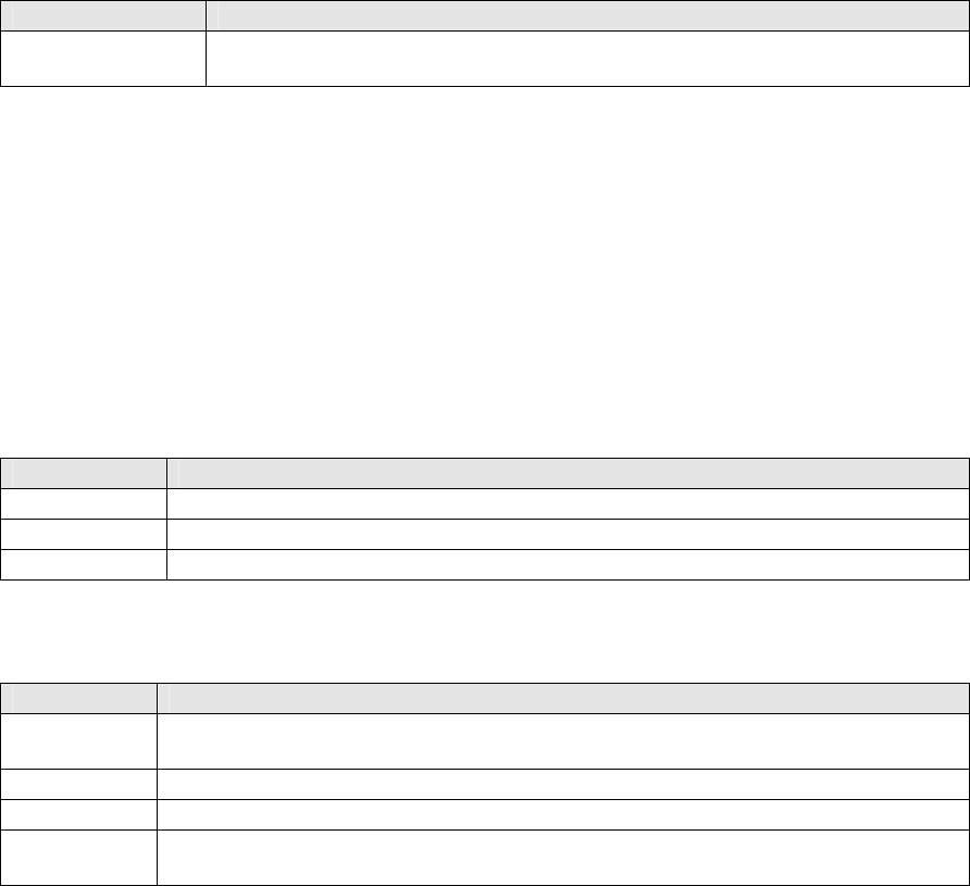
GUARDIAN VHF 110W MOBILE 5-5
Type Description
Individual Call TGID is automatically set to 0000 (hex) and the user ID of the targeted radio is
activated within the Project 25 digital transmit signal
5.3.2 Receiver Characteristics
5.3.2.1 Receiver Performance
The receiver is capable of demodulating a single-channel FM carrier using either conventional 12.5 kHz FM, 25 kHz
FM, C4FM, or compatible quadrature phase shift keying (CQPSK) modulation. The receiver demodulates analog or
digital voice and data signals. The radio circuitry receives clear messages while operating in secure mode, and
secure messages while in the clear mode, if encryption is enabled.
5.3.2.2 Receive Squelch
5.3.2.2.1 Analog Receive Squelch
There are 3 types of analog receive squelch:
Type Description
Carrier (noise) Squelch is opened on any intelligible analog signal
CTCSS Squelch is opened on any analog signal having the correct CTCSS tone
DCS Squelch is opened on any analog signal having the correct DCS variable
5.3.2.2.2 Digital Receive Squelch
There are 4 types of digital receive squelch:
Type Description
Monitor Squelch is opened on any intelligible digital signal. The NAC and talkgroup ID do not
have to match
Normal Squelch is opened on any digital signal having the correct NAC
Selective Squelch is opened on any digital signal having the correct NAC and TGID
Individual call Squelch is opened on a digital signal having a TGID of 0000 (hex) and a user ID matching
that of the receiving radio
5.4 Communication Security
The radio is capable of secure communication by means of type-3, software-based encryption, and is fully
compatible with any radio using Project 25 DES encryption. When the radio is operating in the secure mode, the
transmission of all tone squelch signals is disabled.
5.4.1 Algorithms
The radio is capable of single-bit cipher feedback (SBCF) DES (compatible with other manufacturers) 25 kHz
channels.
5.4.2 Keyfill
Keyfill is accomplished through the radio accessory connector using the PC programmer. The PC programming
cable is used to load the keys. The radio can store up to 16 encryption keys. The radio retains encryption keys until
they are rewritten or zeroized.
5-6 GUARDIAN VHF MOBILE
5.4.3 Zeroize
The radio can be programmed using an optional, external emergency key to zeroize all encryption keys. Using the
programming menu, the radio can also zeroize all encryption keys, or selectively zeroize individual encryption keys.
The emergency key is programmed using the PC programmer.

GUARDIAN VHF 110W MOBILE 6-1
CHAPTER 6: SERVICING THE RADIO
6.1 General
There are no user serviceable parts in the Guardian radio. Return it for servicing to the manufacturer after
requesting an RMA number. Attempts to service the Guardian radio by non-authorized personnel voids the
warranty.
6.2 Self-Test at Power Up
At radio switch-on, the H8 controller executes a number of tests to confirm correct operation. Any errors are
reported to the user through displayed error messages and logged in the Flash. The tests implemented include:
• Flash checksum CRC
• RAM read and write
• FPGA configuration
• DSP host interface
• Keypad interface to AVR
• DC bus interface
• Transceiver EEPROM interface
• Synthesizer lock tests top and bottom frequencies, lock time, etc.
6.3 Caution
Repair of some parts of this unit require special tools and soldering techniques not normally available in a field
service environment. DWC highly recommends the module subassemblies be returned to the factory for service.
Damage can easily occur from repair attempts by non-trained personnel.

GUARDIAN VHF 110W MOBILE 7-1
CHAPTER 7: TROUBLESHOOTING
7.1 Introduction
This chapter is included to help qualified service personnel troubleshoot and repair the Guardian radio. If questions
or problems arise, contact Datron Technical Support Services Group, Datron World Communications Inc., 3030
Enterprise Court, Vista, CA 92083, or phone (760) 597-3755, or email to: guardianservice@dtwc.com. For
additional troubleshooting information, refer to the following sections of this manual:
• Chapter 2: Hardware Theory of Operation
• Chapter 3: Software Theory of Operation
• Chapter 4: Installation, Adjustment and Operation
• Chapter 11: Schematics
This chapter contains basic functional tests. Once the problem is corrected, restart the tests.
7.2 Radio Functional Tests
The tests in this chapter require the radio to be tested as programmed. It is best to program all 3 auxiliary buttons to
Hi/Lo power, the emergency button to emergency, and the toggle switch to zone select. Program the radio with
eighteen channels, 3 zones, and 1 bank. Put 16 channels in zone 1, 1 channel in zone 2, and 1 channel in zone 3. For
all of the channels, use assigned transmit and receive frequencies, turn transmit squelch off, and set receive squelch
to carrier, level 8. When more than one remove and receive tasks are shown in a block, they are listed in order from
most to least probable for fixing the problem. It is recommended that the remove and repair tasks are tried one at a
time, and the radio re-tested until the problem is fixed.
The tests outlined below provide an overall check of the radio to ensure it is working properly.
7.2.1 Power-On Test
This test ensures that the radio turns on, the latest software version number briefly appears, a beep is heard, and an
operational screen appears on the LCD.
7.2.2 Buttons and Switches Test
This test ensures that the PTT, auxiliary buttons, toggle switch, emergency key, keypad, on/off/volume switch, and
channel switch work.
7.2.3 Transmit Test
This test ensures the radio has the required transmit power, frequency accuracy, and deviation.
7.2.4 Receive Test
This test ensures the radio LED works, a 1 kHz tone is heard, and that SINAD is within specified limits.
7.2.5 Audio Test
This test ensures that the radio’s internal speaker and microphone are working. If the radio fails this test, please
contact Datron for radio servicing.
7-2 GUARDIAN VHF MOBILE

GUARDIAN VHF 110W MOBILE 8-1
CHAPTER 8: DEFINITIONS
Alert Mode: Display and audio properties are used when the emergency key is pressed. In normal mode, the display
flashes EMERGENCY and an audio tone is heard. In silent mode, the display is blank and no audio tone is heard.
Analog-to-Digital Converter (ADC): An electronic device for converting data from analog to digital form for use
in electronic equipment.
Backlight: The light behind the keypad and LCD enables the keys and LCD to be visible in dark conditions.
Backlight Delay: The time the backlight remains on after the last keypad activity.
Bandwidth (BW): A small range of frequencies around a transmit or receive frequency in which a message can be
received or transmitted.
Bank: A group of zones. There are up to 4 banks per radio. Up to 16 zones can be distributed through these
4 banks.
Channel: A memory location with defined receive, transmit, squelch, modulation, and power settings. There are
256 channels per radio.
Channel Locked: An indicator informing that channel settings cannot be programmed using the LCD and keypad.
The settings can only be changed using the PC programmer.
Channel Scan: Scans all channels on the scan list in a given 16-channel zone. The scan starts on the home channel,
checks each channel in the scan plan, returns to the home channel, and then scans each channel in the scan plan.
Common Air Interface (CAI): The CAI standard allows interoperability within any Project 25 system provided
they are all in the same frequency band.
Continuous Tone-Controlled Squelch System (CTCSS) Tone: A sub-audible tone superimposed on an analog
signal to reduce interference from traffic and background noise.
Digital Coded Squelch (DCS): A digital variable superimposed on a digital signal to reduce interference from
traffic and background noise.
Digital Signal Processor (DSP): Handles all signal-processing functions.
Digital to Analog Converter (DAC): A device that takes a digital value and outputs a voltage that is proportional to
the input value.
Dual-Tone Multiple-Frequency (DTMF): A signaling scheme used by the telephone system in which two-voice
band tones are generated for each keypad key press.
Global Search: Scans all frequencies programmed into the radio, regardless of scan list designation.
Initial Synchronization: The length of time required for the radio to perform encryption synchronization.
Microprocessor Unit (MPU): A computer’s entire CPU is contained on one (or a small number of) integrated
circuit.
Monitor Receive Squelch: The radio receives any intelligible analog transmission.
Monitor Timer: The amount of time the radio stays on a channel picked up during the scan and before the radio
reverts back to scan mode.
Network Access Code (NAC): Selective squelch for digital mode. The primary purpose is to allow the user access
to a repeater network. In radio-to-radio communications, these codes are used to eliminate interference from other
traffic and background noise.
Normal Receive Squelch: The radio receives any transmission having the correct NAC.
Priority 1 Scan: Priority 1 channel is sampled during scanning, receive of an active channel, or standby. Activity
on the priority1 channel overrides all other modes except emergency.
8-2 GUARDIAN VHF MOBILE
Priority 2 Scan: Priority-2 channel is sampled in a similar fashion to the priority-1 channel. Activity on the
priority-2 channel overrides all other modes except emergency and priority 1.
Receive Only Channel: A feature that does not allow outgoing transmissions on the channel. It is used for channels
in which transmission is prohibited (i.e., weather channels). If PTT is pressed on a receive-only channel, RX ONLY
appears on the display.
Receiver/Exciter/Control Module (RECM): Transceiver module containing all radio functions except RF/audio
amplifiers and display/keypad circuitry.
Repeater Delay: A delay timer used to prevent a radio from receiving its own transmission from a tactical repeater.
Scan Delay: The amount of time the scanner dwells on an active receive channel after the carrier is dropped. This
prevents another message from being received before a response can be made.
Scan Reply: If a PTT press interrupts the scan delay timer, this is the amount of time allowed to ensure a reply to a
received message.
Scan List: A group of channels in a zone that are designated as active scan list channels. Channels are added or
deleted from the scan list using the PC programmer or the radio keypad.
Scan Revert Channel: The transmit channel that the radio reverts to when PTT is pressed during or following a
scanned message.
Search Mode: The radio scans for and opens on carrier only regardless of CTCSS, DCS, or the digital ID.
Selective Receive Squelch: The radio receives any transmission having the correct NAC and TGID.
Shadow Channel: The radio of primary channels, each of which can have up to 7 shadow channels. A shadow
channel has the same transmit and receive frequencies, options, and transmit power levels as its primary channel.
Individual shadow channels can be configured for different channel types (analog or digital), BW (12.5 or
25 kHz for analog channels), squelch modes, P25 NACs (digital channel only), and encryption key (only one primary
or shadow channel can have CVSD DES enabled). When properly configured, shadow channels can be created to
allow a user to hear all transmissions on a receive/transmit frequency regardless of channel type, BW, squelch mode,
or encryption. Shadow channels are created and their settings edited using the PC programmer.
Talk Group Identifier (TGID): Selective squelch for the digital mode, used to group users into functional teams.
Transmit Inhibit and Override: A feature that stops users from talking over other radio conversations. There are
three options: CARRIER prevents transmission if any activity is detected on the channel, TONE prevents
transmission on an active channel with a squelch code other than your own, and NAC prevents transmission on an
active channel with the same NAC. There is a quick-key override feature available that allows a user to override the
transmit inhibit state by quick-keying the radio (i.e., 2 PTT presses within a short time frame).
Transmit Timeout: Prevents inadvertent or prolonged transmit operations.
User Interface: The same as a man-machine interface.
Zone: A group of channels. There is a maximum of 16 zones per radio and each zone can contain up to 16 channels.
Three zones can be selected using the toggle switch or 16 zones selected by the radio keypad.
Zone Scan List: A group of zones in a bank designated as active scan list zones. Zones are added or deleted from
the scan list using the PC programmer or the radio’s keypad.

GUARDIAN VHF 110W MOBILE 9-1
CHAPTER 9: SIGNAL TONES
Tone Signal Cause
Key press error Invalid key pressed
Failed power on self-test (POST) Radio fails POST
Transmit time-out warning Time-out about to interrupt PTT
Brief low-pitched
Empty channel warning No RX/TX frequencies programmed for the
channel
Transmit time-out timed out Transmit time is exceeded and PTT still pressed
Transmit inhibit PTT switch is pressed and there is activity on the
transmit channel
Invalid mode No programmed data on the selected channel
Steady low-pitched
Radio locked Radio locks after 3 consecutive wrong password
attempts
Key press Valid key press is accepted by the radio
Radio passed POST Radio passed POST
Brief medium-pitched
Clear voice received Radio is receiving a clear signal
Emergency call state Emergency button is pressed Repeated medium-pitched
Key error Encryption is selected but no key is present
Brief high-pitched Low dc supply voltage DC supply voltage falls below a preset value
Repeated high-pitched Individual call An individual call is received
9-2 GUARDIAN VHF MOBILE

GUARDIAN VHF 110W MOBILE 10-1
CHAPTER 10: CONNECTOR PINOUTS
10.1 Accessory Connector Pins and Functions
Pin Signal Name Description
1 RS232_RXD Receive data line output (DCE), RS232 level
(>+3V=ZERO, <-3V=ONE)
2 RS232_RTS Data port control input (DCE), RS232 level (>+3V=ON, <-3V=OFF)
3 SERIAL_CLOCK Synchronous clock output to PC terminal (DCE), RS232 level
(>+3V=ZERO, <-3V=ONE)
4 RS232_CTS Data port control output (DCE), RS232 level (>+3V=ON, <-3V=OFF)
5 PC_232RXD Programming receive data line output (DCE), RS232 level
(>+3V=ZERO, <-3V=ONE)
6 SQUELCH_INF Squelch, low on valid receive signal, 7.8V squelched
7 GND Ground
8 EXTERNAL_SPEAKER_N Balanced audio output from RECM, 500 mW into 8 ohms
9 EXTERNAL_PTT/KID PTT input asserted by voltage closure to ground or pseudo-random key
insert data, LVTTL level input
10 7.7V Test point for internal regulated voltage supply
11 EXTERNAL_MIC/WE Microphone input or key transfer indicator input, asserted by voltage
0.8 Vdc
12 GND Ground
13 INTERNAL_SPEAKER_P Balanced audio input from external device; can override RECM audio
output signal
14 PTT_SWITCH PTT input asserted by voltage closure to ground
15 RS232_DTR Data port control input (DCE), RS232 level (>+3V=ON, <-3V=OFF)
16 PC_232TXD Programming transmit data line input (DCE), RS232 level
(>+3V=ZERO, <-3V=ONE)
17 RS232_TXD Transmit data line input (DCE), RS232 level
(>+3V=ZERO, <-3V=ONE)
18 WRU_MONITOR Voltage input identifies external device
19 EXT_10W_SPEAKER_N Balanced audio output for external 10W 4-ohm speaker
20 EXT_10W_SPEAKER_P Balanced audio output for external 10W 4-ohm speaker
21 EXTERNAL_MIC_BIAS/KEY Microphone bias or bi-directional key data, LVTTL levels
22 EXTERNAL_SPEAKER_P/KLD Balanced audio output from RECM, 500 mW into 8 ohms or LVTTL
low-output level when keyloader is connected
23 EMERGENCY_SWITCH Active low control to transmit emergency signal
24 IGN_SW Power switch override input. Ground forces off, open enables switch
25 INTERNAL_SPEAKER_N Balanced audio input from external device; can override RECM audio
output signal

10-2 GUARDIAN VHF MOBILE
10.2 Power Connector Pins and Functions
Pin Signal Name Description
1 BATTERY Battery power
2 GROUND Ground
3 IGN_SW Ignition switch
4 EXTERNAL_10W_SPEAKER_N External speaker
5 EXTERNAL+10W_SPEAKER_P External speaker
6 BATTERY Battery power
7 GROUND Ground
8 GROUND Ground
9 EMERGENCY_SWITCH Emergency switch
10.3 Microphone Jack Connector Pins and Functions
Pin Signal Name Description
1 EXTERNAL_MIC_BIAS/KEY Keyload line
2 GROUND Ground
3 INTERNAL_MIC Microphone audio
4 EXTERNAL_MIC/WE Keyload line
5 PTT_SWITCH Push-to-talk line
6 BIAS(+) Microphone power
7 EXTERNAL_SPEAKER_P/KLD Keyload line
8 EXTERNAL_PTT/K1D Keyload line

GUARDIAN VHF 110W MOBILE 11-1
CHAPTER 11: SCHEMATICS
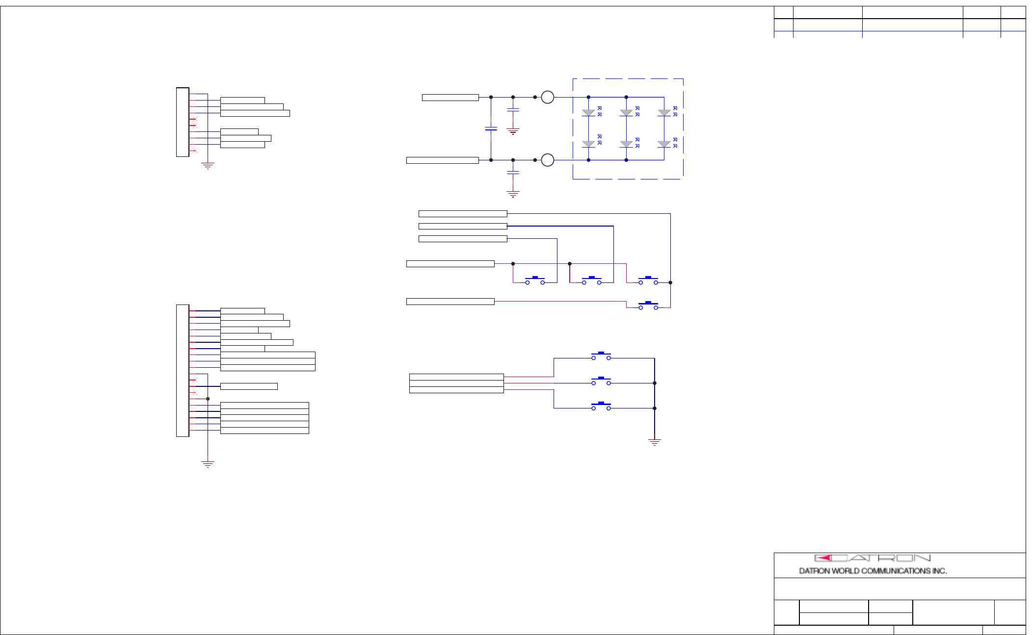
11
994466 A
14-May-2002 11:06:32994466A.Sch
Title:
Size: Drawing Number:
Date:File:
Rev:
Sheet of
Time:
SCHEMATIC, KEYPAD/DISPLAY
Schematic
Date:
Date:
Appr:
Drawn:
REV ECN DESCRIPTION DATE APPR
3030 Enterprise Ct.
Vista, CA 92083
(760)597-3777
B
LCD_CLOCK
LCD_TX
LCD_CS_N
LCD_RESET_N
LCD_DATA_MODE
V3.3_LCD
AUXILLARY_SWITCH_1
AUXILLARY_SWITCH_2
AUXILLARY_SWITCH_3
S4
ENTER
S3
MENU KEY 3
S2
MENU KEY 2
S1
MENU KEY 1
KEYPAD_SCAN_OUT_1
KEYPAD_SCAN_OUT_2
KEYPAD_SCAN_OUT_3
KEYPAD_SCAN_IN_1
KEYPAD_SCAN_IN_2
S5
MENU KEY 1
S6
MENU KEY 1
S7
MENU KEY 1
LCD_CLOCK
LCD_TX
LCD_CS_N
LCD_RESET_N
LCD_DATA_MODE
V3.3_LCD
AUXILLARY_SWITCH_1
AUXILLARY_SWITCH_2
AUXILLARY_SWITCH_3
KEYPAD_SCAN_OUT_1
KEYPAD_SCAN_OUT_2
KEYPAD_SCAN_OUT_3
KEYPAD_SCAN_IN_1
KEYPAD_SCAN_IN_2
ABE SABET 04-12-01
A 02-0128 RELEASE 02-19-02
+7.7V
+7.7V C1
.01
PART OF LCD MODULE 320803
LCD_BACKLIGHT
LCD_BACKLIGHT
1
2
3
4
5
6
7
8
9
10
11
12
13
14
15
16
17
18
19
20
P13
620171
8
1
2
3
4
5
6
7
10
9
J9
080010002
C2
.01
BB
C3
.01
E1
E2
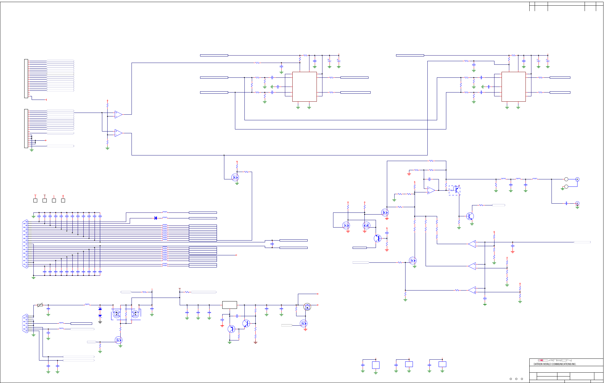
11
994478 A
14-May-2002 10:55:16994478A.Sch
Title:
Size: Drawing Number:
Date:File:
Rev:
Sheet of
Time:
D
AUDIO AMP BD, GUARDIAN 100W MOBILE
Schematic
Date:
Date:
Appr:
Drawn:
REV ECN DESCRIPTION DATE APPR
3030 Enterprise Ct.
Vista, CA 92083
(760)597-3777
INT_5W_SPEAKER_P
INT_5W_SPEAKER_N
INTERNAL_SPEAKER_P
AUDIO_INTERNAL_DISABLE
R10
10K
EXTERNAL_10W_SPEAKER_N
EXTERNAL_10W_SPEAKER_P
INTERNAL_SPEAKER_N
AUDIO_EXT_DISABLE
+IN1
1
--IN1
2
GND1
3
Vref
4
OUT1 5
BS1 6
GND2
7
BS2 8
OUT2 9
Vp 10
M/SS 11
RR
12
+IN2
13
U2
TDA1516BQ
C5
1uF/25V
C4
1uF/25V
R16
10k
R15
10k R33
10k
R13
10k
R14
10k
R19
10k SWBAT
R4
0ohm
R5
0ohm
+IN1
1
--IN1
2
GND1
3
Vref
4
OUT1 5
BS1 6
GND2
7
BS2 8
OUT2 9
Vp 10
M/SS 11
RR
12
+IN2
13
U1
TDA1516BQ
C1
1uF/25V
C2
1uF/25V
R9
10k
R8
10k R21
10k
R6
10k
R7
10k
R12
10k
SWBAT
R2
0ohm
R3
0ohm
C14
0.1uF
C15
0.1uF
C22
47uF,20V
C21
47uF,20V
C19
47uF,20V
C20
47uF,20V
INTERNAL AUDIO AMPLIFIEREXTERNAL AUDIO AMPLIFIER
C3
1uF/25V C6
1uF/25V
R17
10K
C7
1nF
C8
1nF
R18
10k
R11
10k
Q5
2N7002
R43
0ohm
C55
1uF/25V
J4
OSMT
C9
1nF C10
1nF
L1
2.7uH
R46
100k
R23
1k
R24
1k
R44
100K
R34
10k
R26
10k
R22
10k
R35
10k
R27
300
R38
2.67K-1%
R30
10k
R32
10k
R28
10k
PA_PTT
3
2
1
U4A
LM2903
4 8
VCC
GND U3C
LM2904
1
2
3
U3A
LM2904
Q7
2N7002
7.8Vsw
LED_TX
7.8Vsw
C16
0.1uF
C53
10uF
EMERGENCY_SWITCH
EXTERNAL_10W_SPEAKER_P
EXTERNAL_10W_SPEAKER_N
L2
10uH C13
1nF
SWBAT
RS232_RTS
SQ_INF
RS232_CTS
EXTERNAL_10W_SPEAKER_N
RS232_DTR
EXTERNAL_10W_SPEAKER_P
RS232_TXD
RS232_RXD
INTERNAL_SPEAKER_P
PC_232TXD
SERIAL_CLOCK
PC_232RXD
EXTERNAL_MIC/WE
EXTERNAL_PTT/KID
EXTERNAL_SPEAKER_N
PTT_SWITCH
WRU_MONITOR
EXTERNAL_MIC_BIAS/KEY
EMERGENCY_SWITCH
EXTERNAL_SPEAKER_P/KLD 7.8Vsw
INTERNAL_SPEAKER_N
1
14
2
15
3
16
4
17
5
18
6
19
7
20
8
21
9
22
10
23
11
24
12
25
13
J6
610458
FB23
FB22
FB21
FB20
FB19
FB17
FB16
FB15
FB14
FB13
FB12
FB11
FB10
FB9
FB8
FB7
FB6
FB5
FB4
C52
100pF
FB18
C26
100pF
C27
100pF
C28
100pF
C29
100pF
C30
100pF
C31
100pF
C32
100pF
C35
100pF
C36
100pF
C38
100pF
C39
100pF
C41
100pF
C42
100pF
C43
100pF
C44
100pF
C45
100pF
C46
100pF
C47
100pF
C48
100pF
C50
100pF
C51
100pF
C40
100pF
C49
100pF
R36
10k
ON/OFF
R39
1.27k-1%
Q9
MMBT2222
R45
0OHM
FB1 FB2
SWBAT
C17
0.1uF
C33
100pF
C34
100pF
C25
.01uF
C37
100pF
FB3
E1
PAD
E2
PAD
C12
1nF
5
6
7
U4B
LM2903
8
4
U4C
LM2903
SWBAT
C18
0.1uF
75
6
U3B
LM2904
R37
0ohm
R53
10k
R55
560
R54
1.82K-1%
J3
1
2
3
4
5
6
7
8
9
J5
610457
2
4
1
3
7,8 5,6
Q10
IRF7328
FB24
D3
4148
R60
10k
C58
1nF
R56
1.05K,1%
R52
10k
7.8Vsw
7.8Vsw
IGN_SW
IGN_SW
PF1
550044
PANEL MNT
VBAT
7.8Vsw
C56
1uF/25V
R41
51.1K-1%
Q8
10K/10K
3
21
U6A
LM2903
8
4
U6C
LM2903
5
67
U6B
LM2903
R20
100k
R1
200k
7.8Vsw
Q1
2N7002
R29
100
R40
10k
7.8Vsw
R50
2.67K
C82
1uF/25V
C57
DNP
Vout 2
1
+Vin
3
ADJ
U5
LM350T
C11
10uF
R51
12.7K
R47
100K
Q3
MMBT2907
Q2
MMBT2222
R49
1.05K,1%
SWBAT
C23
0.1uF
R48
10k
1
2
3
4
5
6
7
8
9
10
11
12
13
14
15
16
17
18
19
20
J1
613507
1
2
3
4
5
6
7
8
9
10
11
12
13
14
15
16
17
18
19
20
J2
613507
3.3V VBAT SWBAT 7.8V
FB25
Q12
IRLML6302
Q11
2N7002
ON/OFF
R62
10K
7.8V
D1
1N6278
D4
1N6278
Q15
2N7002
Q14
2N7002
Q13
2N7002
Q16
MMBT2222
R63
100k R64
100k
7.8Vsw7.8Vsw
7.8Vsw
R65
100k
C24
1uF/25V
PTT_SWITCH
TP21
3.3V SWBATVBAT 7.8V
R66
DNP
R67
0OHM
R69
10k
R68
270
ON/OFF
PA_PTT
LED_TX
INT_5W_SPEAKER_N
INT_5W_SPEAKER_P
AUDIO_INTERNAL_DISABLE
AUDIO_EXT_DISABLE
INTERNAL_SPEAKER_P
INTERNAL_SPEAKER_N
EXTERNAL_SPEAKER_P/KLD
EXTERNAL_MIC_BIAS/KEY
WRU_MONITOR
RS232_TXD
PC_232TXD
RS232_DTR
EXTERNAL_MIC/WE
EXTERNAL_PTT/KID
PC_232RXD
RS232_CTS
SERIAL_CLOCK
RS232_RTS
RS232_RXD
EXTERNAL_SPEAKER_N
7.8V
PTT_SWITCH
SQUELCH_INDICATOR
IGN_SW
EMERGENCY_SWITCH
3.3V
TP21
BIAS
BIAS
VBAT_TP
VBAT_TP
C54
1nF
R25
6.2K
FD1FD2FD3
BOM:125-50220
PCB:738534
C38
DNP
R31
0OHM
R42
0OHM
R57
0OHM
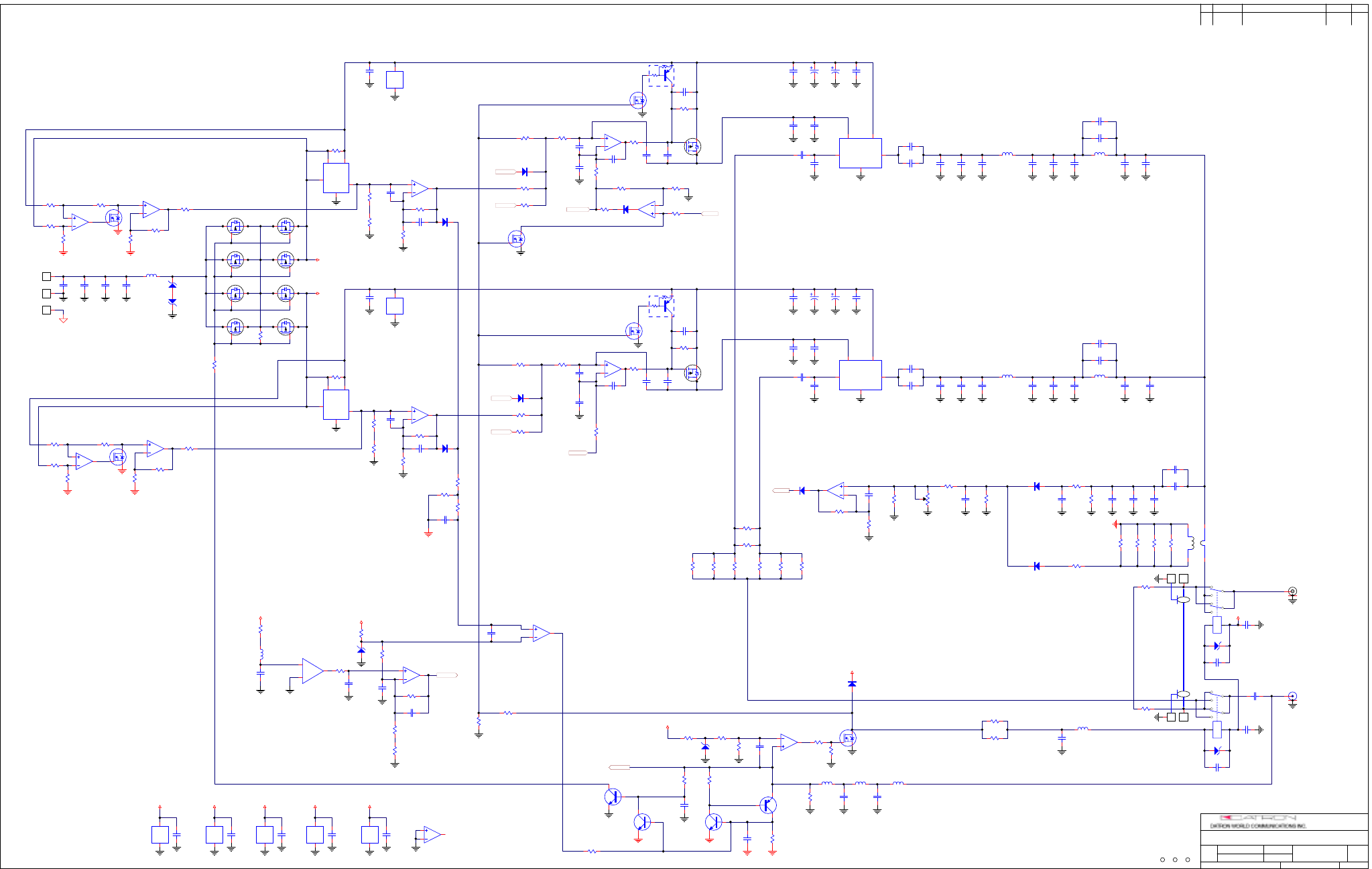
11
994483 A
14-May-2002 10:56:49994483A.sch
Title:
Size: Drawing Number:
Date:File:
Rev:
Sheet of
Time:
D
GUARDIAN MOBILE, 110WPA
Schematic
Date:
Date:
Appr:
Drawn:
REV ECN DESCRIPTION DATE APPR
3030 Enterprise Ct.
Vista, CA 92083
(760)597-3777
C26
.01uF
C37
1nF
L7
68nH
E2
E1
C62
47uF,20V C63
47uF,20V
C35
1uF/25V
SWBAT2
R36
1k C32
.01uF
C28
.01uF
BATT+
BATT-
C14
0.1uF
C16
1uF/25V
R40
DNP
C10
DNP
4 8
VCC
GND
U6C
LM2904
D1
MMBD4148
R28
0ohm
1
2
3U3A
LM2904
C1
100pF
C11
DNP
R12
10k
1
2
3
U4A
LM2904
C20
1uF/25V
R8
0.01ohm-1%
SWBAT1
C9
100pF
C3
100pF
L3
74nH
C72
DNP
R25
10K
1
2
3
LM35
U12
LM35
TEMP SENSOR
Q9
IRF4905
C39
1nF
C17
1uF/25V
C27
.01uF
FB2
FB
C23
1uF/25V C8
100pF
C94
2.2pF
C105
1nF
R75
8.25k
C33
DNP
R15
10k
R87
402k
R85
6.19k
R86
5.62k
R2
100k
R6
100k
C67
.001uF
C66
.001uF
R26
1k
C53
1nF
C54
18pF
D10
1N6278
OUT 1
Vin+ 3
V+
5
GND
2
Vin- 4
U1
DNP
C55
6.8pF C81
DNP
R39
1k C29
.01uF
C40
1nF
C64
47uF,20V C65
47uF,20V
C30
.01uF
C19
0.1uF
C21
1uF/25V
R42
DNP
C12
DNP
7
5
6
U6B
LM2904
D3
MMBD4148
R30
0ohm
C2
100pF
C13
DNP
R19
10k
4 8
VCC
GND
U3C
LM2904
C4
100pF
Q10
IRF4905
C22
1uF/25V
C31
.01uF
C34
DNP
R22
10k
R57
20.5k
R4
100k
C58
18pF
OUT 1
Vin+ 3
V+
5
GND
2
Vin- 4
U2
DNP
M68702H
RF_IN
1
DC1 2
DC2 3
RF_OUT 4
GND
5
U9
701363
M68702H
RF_IN
1
DC1 2
DC2 3
RF_OUT 4
GND
5
U10
701363
Vdet
R18
10k
R11
10k
Vdet
Vtemp
Vdet
D4
MMBD4148
Vtemp
D2
MMBD4148
Vtemp
Vref
R33
1k
R32
1k
4 8
VCC
GND
U4C
LM2904
C15
1uF/25V
7
5
6
U4B
LM2904
C106
DNP
4
3
5
112
9
10
8
K2
TX2SA-5V-X
4
3
5
112
9
10
8
K1
TX2SA-5V-X
D14
6.8V
SWBAT1
C51
1nF
C49
1nF
FB5
FB
L1
115uH
ANTENNA
RADIO
FB4
FB
FB3
FB
C47
1nF C48
1nF
L12
2.7uH
7
5
6
U3B
LM2904
4 8
VCC
GND
U7C
LM2904
1
2
3U6A
LM2904
C25
1uF/25V
SWBAT1
R55
0.01ohm-1%
R63
100k
SWBAT1
7
5
6U7B
LM2904
Q12
2N7002
R37
20.5K R27
10k
R59
20.5K
R58
20.5K
SWBAT2
Vref
R3
68k
R5
100k
Vref
C98
0.1uF C100
10uF
C18
1uF/25V
R7
10k
12
3
U7A
LM2904
D5
MMBD4148
R20
5.62K 1%
R34
1k
R48
100k
Vdet
R66
0ohm
D13
6.8V
R88
1.8K
R72
100-1/2W
R71
100-1/2W
SWBAT1
Q11
2N7002
R62
100k
C99
0.1uF
D12
6.8V
C50
1nF
C52
1nF
C46
1nF
R50
10ohm
R51
10ohm
C41
1nF
C38
1nF
C70
10pF C73
DNP
C95
2.2pF
C57
DNP
C69
.001uF
C68
.001uF
C103
6.8pF
C5
1uF/25V 7
5
6
U8B
LM2904
SWBAT2
12
3
U8A
LM2904
4 8
VCC
GND
U8C
LM2904
J1
080002001
J2
610551
R92
0ohm
R31
1k R41
1k
D15
6.8V
R89
68K
R21
7.5K
Q4
MMBT2222
R46
2.7K
R14
330 C80
150pF C82
150pF C83
DNP
C84
4.7pf
C43
10pF C71
12pF
L4
68nH
L2
74nH
C60
DNP
C75
2.2pF
C42
6.8pF C77
DNP
C56
10pF C61
DNP
C76
2.2pF
C78
DNP
C59
10pF C74
12pF
R13
51.1K
R61
100k
E4
E5
E7 E6
E3
+
-
CHASSIS
GND
R17
150-1/2W R23
150-1/2W R24
150-1/2W R29
150-1/2W R35
150-1/2W R38
150-1/2W
4
2
3
1
T1
CURRENTXFMR
R44
100
R47
100
VR1
10K/11T
R9
100K
Q6
DTA114EKA
Q5
2N7002
Q8
DTA114EKA
Q7
2N7002
COAX BYPASS-WHEN INSTALLED
R49
DNP
R67
150
R65
150
R64
150
R60
150
D8
MMBD4148
Q13
MMBT2222 Q14
MMBT2222
Q15
MMBT2907
R53
10k
R69
10k
R68
10k
D7
MMBD4148
D6
MMBD4148
R45
100k
R52
68K
R54
30.1K
C79
1uF/25V
Q1
TPC8106-H Q17
TPC8106-H
Q2
TPC8106-H Q18
TPC8106-H
R1
10k
Q3
TPC8106-H Q19
TPC8106-H
Q16
TPC8106-H Q20
TPC8106-H
D9
1N6278
C6
1uF/25V
1
2
3
U5A
LM2904M 7
5
6U5B
LM2904M
4 8
VCC
GND
U5C
LM2904
C24
1uF/25V
SWBAT1
1
2
3
U11A
LM2904M 7
5
6U11B
LM2904M
4 8
VCC
GND
U11C
LM2904
C7
1uF/25V
SWBAT2
Q22
2N7002
R81
DNP
R80
DNP
R82
DNP
R76
15K
R74
15K
R43
4.99K
R56
4.99K
Q21
2N7002
R79
DNP
R78
DNP
R77
DNP
R70
15K
R73
15K
R10
4.99K
R16
4.99K
FD1
FDU
FD2
FDU
FD3
FDU
PCB:738536
BOM:125-50110
SWBAT2
SWBAT2
R84
1K
R83
DNP
D11
MMBD4148
C36
100pF
C44
DNP
C45
DNP
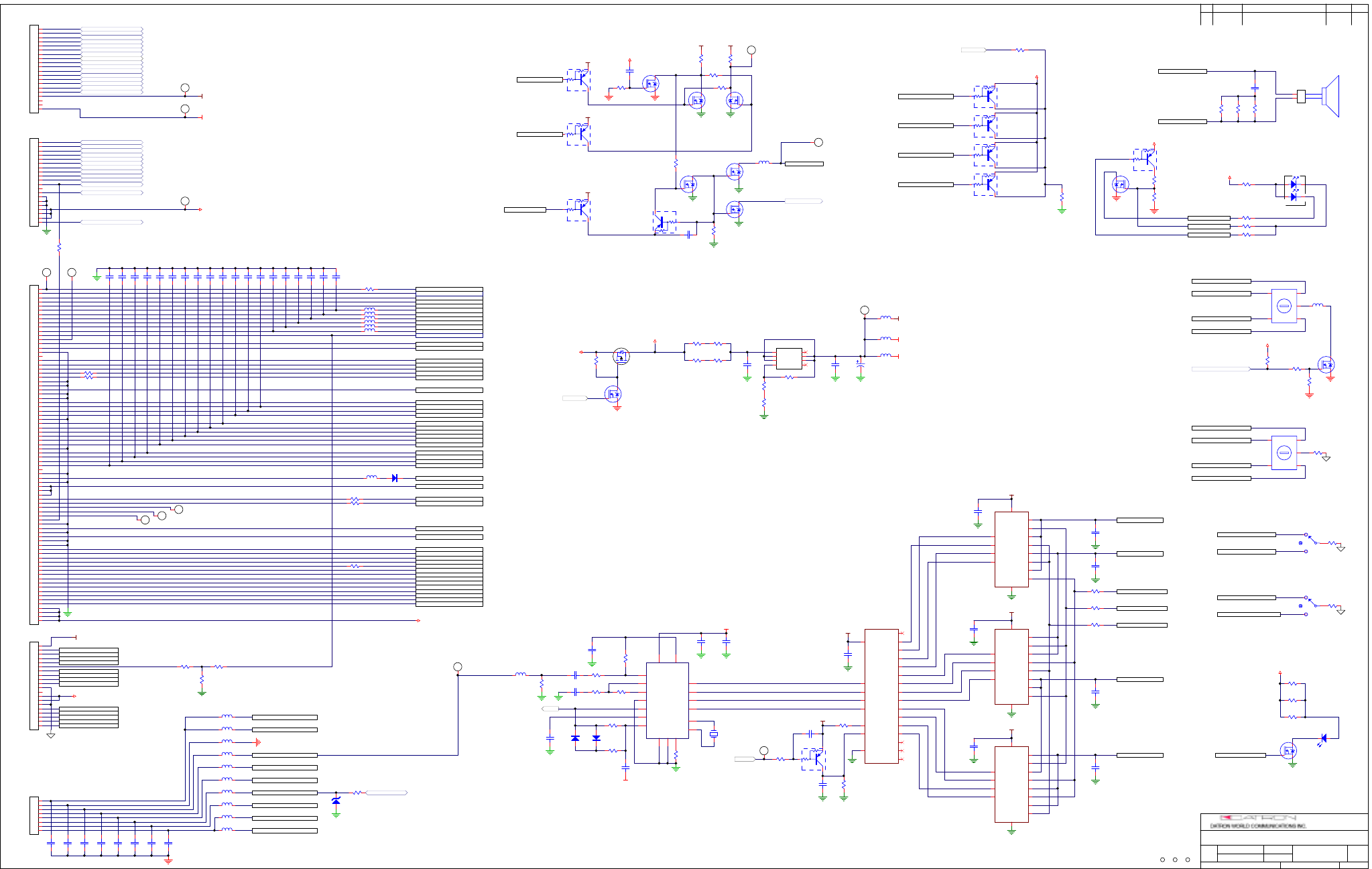
11
994484 A
14-May-2002 10:57:49994484A.sch
Title:
Size: Drawing Number:
Date:File:
Rev:
Sheet of
Time:
D
GUARDIAN 100W MOBILE, CONTROL BD
Schematic
Date:
Date:
Appr:
Drawn:
REV ECN DESCRIPTION DATE APPR
3030 Enterprise Ct.
Vista, CA 92083
(760)597-3777
11
22
33
44
55
66
77
88
99
10 10
11 11
12 12
13 13
14 14
15 15
16 16
17 17
18 18
19 19
20 20
21 21
22 22
23 23
24 24
25 25
26 26
27 27
28 28
29 29
30 30
31 31
32 32
33 33
34 34
35 35
36 36
37 37
38 38
39 39
40 40
41 41
42 42
43 43
44 44
45 45
46 46
47 47
48 48
49 49
50 50
51 51
52 52
53 53
54 54
55 55
56 56
57 57
58 58
59 59
60 60
61 61
62 62
63 63
64 64
65 65
66 66
67 67
68 68
69 69
70 70
71 71
72 72
73 73
74 74
75 75
76 76
77 77
78 78
79 79
80 80
J1
610354
LCD_CLOCK
LCD_TX
LCD_CS_N
LCD_RESET_N
LCD_DATA_MODE
KEYPAD_SCAN_OUT_1
KEYPAD_SCAN_OUT_2
KEYPAD_SCAN_OUT_3
KEYPAD_SCAN_IN_3
KEYPAD_SCAN_IN_4
KEYPAD_SCAN_IN_5
KEYPAD_SCAN_IN_6
INTERNAL_SPEAKER_P
INTERNAL_SPEAKER_N
INTERNAL_MIC
INTERNAL_PTT
AUXILLARY_SWITCH_3
AUXILLARY_SWITCH_2
AUXILLARY_SWITCH_1
VOLUME_SWITCH_1
VOLUME_SWITCH_2
VOLUME_SWITCH_3
VOLUME_SWITCH_4
TOGGLE_SWITCH_1
TOGGLE_SWITCH_2
CHANNEL_SWITCH_1
CHANNEL_SWITCH_2
CHANNEL_SWITCH_4
CHANNEL_SWITCH_3
EMERGENCY_SWITCH
LED_RED_N_SYS
LED_GREEN_N
EXTERNAL_MIC_BIAS/KEY
EXTERNAL_MIC/WE
WRU_MONITOR
EXTERNAL_PTT/KID
EXTERNAL_SPEAKER_N
EXTERNAL_SPEAKER_P/KLD
PC_232TXD
PC_232RXD
RS232_RTS
RS232_CTS
RS232_DTR
RS232_TXD
RS232_RXD
SERIAL_CLOCK
RADIO_OFF_SC_N
SQUELCH_INDICATOR
D2
4148
Q1 11
Q2 12
Q3 13
Q4 14
TOE
10
StD
15
ESt
16
INH
5
VDD 18
VREF 4
VSS
9
IN+
1
IN-
2
GS
3
PD
6
St/GT
17 OSC1 7
OSC2 8
U6
CM88L70
R47
DNP
D7
DNP
D6
DNP
3.3DTMF
R13
100k
R14
100k
C54
.01uF
C53
.01uF
C26
0.1uF
C40
47uF,20V
C22
0.1uF
ESt
Y1
3.579545 MHZ
C21
0.1uF
3.3V
C28
0.1uF C29
0.1uF
FB13
FB R45
DNP
PTT_SWITCH
KEYPAD_SCAN_IN_1
KEYPAD_SCAN_IN_2
R43
560
FB11
FB
R25 0ohm
R24 DNP
3V3_LOGIC
FB9
FB
VOLUME_SWITCH_1
VOLUME_SWITCH_2
VOLUME_SWITCH_3
VOLUME_SWITCH_4
ON/OFF
FB8
FB
AUDIO
INTERNAL_PTT
FB7
FB INTERNAL_PTT
1Y 1
1Z 2
2Y 4
4E
12
2Z 3
3Y 8
3Z 9
4Y 11
4Z 10
2E
5
1E
13
3E
6
VEE
7VCC 14
U3
74HC4016
Y5 6
Y0 11
Y2 10
Y1 9
GND
12
Y13 13
A0
2
/LE
1
Y6 5
A1
3
Y15 15
Y12 14
Y7 4
Y4 7
Y14 16
Y3 8
Y8 18
Y9 17
Y11 19
Y10 20
A2
21
A3
22
/E
23
Vcc
24
U2
74HC4514
1Y 1
1Z 2
2Y 4
4E
12
2Z 3
3Y 8
3Z 9
4Y 11
4Z 10
2E
5
1E
13
3E
6
VEE
7VCC 14
U5
74HC4016
K1
K2
K3
K4
K5
K6
K7
K8
K9
K*
K0
K#
KEYPAD_SCAN_IN_5
KEYPAD_SCAN_IN_6
KEYPAD_SCAN_IN_3
KEYPAD_SCAN_IN_4
KEYPAD_SCAN_OUT_1
KEYPAD_SCAN_OUT_2
KEYPAD_SCAN_OUT_3
3.3DTMF
3.3DTMF
3.3DTMF
3.3DTMF
C23
0.1uF
C25
0.1uF
3.3DTMF
47K
Q2
DTA144EK
47K
Q10
DTA144EK
47K
Q3
DTA144EK
Q7
2N7002
KEYPAD_SCAN_IN_2
R35
100
R36
100
R37
100
R38
100
R46
270k
C27
0.1uF
R50
DNP ESt
47K
Q4
DTA144EK
R29
0ohm
R15
100k
KEYPAD_SCAN_IN_1
47K
Q1
DTA144EK
3.3V
R28
0ohm
R26
0ohm
R27
0ohm
C24
0.1uF
C30
0.1uF
1Y 1
1Z 2
2Y 4
4E
12
2Z 3
3Y 8
3Z 9
4Y 11
4Z 10
2E
5
1E
13
3E
6
VEE
7VCC 14
U4
74HC4016
FB10
FB 3.3DTMF
3.3DTMF
C39
DNP
ON/OFF
R22
1M
E4
PAD
E8
PAD
E9
PAD
E10
PAD
R2 1k
R1 1k
R21 10k
C42
DNP
C43
DNP
C44
DNP
C33
1uF/16V
R49
220K
R48
220K
10K
Q11
DTA114EKA
10K
Q12
DTA114EKA
10K
Q13
DTA114EKA
10K
Q14
DTA114EKA
C41
DNP
R20
10k
C32
1uF/16V
R51
47.5k
Q5
2N7002
Q6
2N7002
Q8
2N7002
3.3V 3.3V
C31
1uF/16V
(ESCAPE)
(ENTER)
R16
10k
R17
10k
R19
10k
R18
10k
R12
100k
R3
1k
FB6
FB5
FB4
FB3
FB2
FB1
C1
DNP
C2
DNP
C3
DNP
C4
DNP
C5
DNP
C6
DNP
C7
DNP
C8
DNP
C9
DNP
C10
DNP
C11
DNP
C12
DNP
C13
DNP
E1
PAD E2
PAD
E7
PAD
E6
PAD
E5
PAD
D4
12V
C14
100p C15
100p C16
100p C17
100p C18
100p C19
100p
E3
PAD
+3.3V_LCD
PCB: 738535
BOM: 125-50210
1
2
3
4
5
6
7
8
J5
610669
BIAS(+)
PTT_SWITCH
EXTERNAL_MIC/WE
INTERNAL_MIC
EXTERNAL_SPEAKER_P/KLD
EXTERNAL_PTT/KID
L8
FB
C52
100p
L7
FB
C45
100p
L6
FB
C51
100p
L5
FB
C50
100p
L4
FB
C49
100p
L3
FB
C48
100p
L2
FB
C47
100p
L1
FB
C46
100p
1
2
3
4
5
6
7
8
9
10
11
12
13
14
15
16
17
18
19
20
J4
621112
LCD_CLOCK
LCD_TX
LCD_RESET_N
LCD_DATA_MODE
AUXILLARY_SWITCH_1
AUXILLARY_SWITCH_2
AUXILLARY_SWITCH_3
KEYPAD_SCAN_OUT_1
KEYPAD_SCAN_OUT_2
KEYPAD_SCAN_OUT_3
KEYPAD_SCAN_IN_1
KEYPAD_SCAN_IN_2
LCD_CS_N
+3.3V_LCD
R40
0ohm
7.8Vsw
LED_TX
LED_GREEN_N
VOLUME_SWITCH_3
VOLUME_SWITCH_4
12
84
C
SW3
510038
VOLUME_SWITCH_1
VOLUME_SWITCH_2
R33
100
R30
DNP R31
DNP R32
DNP
C38
DNP
INT_5W_SPEAKER_P
INT_5W_SPEAKER_N
RED
GRN
D3
035500004
VOLUME
12
84
C
SW4
510038
AUDIO_EXT_DISABLE
CHANNEL_SWITCH_1
CHANNEL_SWITCH_2
CHANNEL_SWITCH_4
CHANNEL_SWITCH_3
R39 100
R34
330
CHANNEL
Q9
2N7002
FB12
FB
IN
1
OUT3
3OUT2
2
ADJ
4
NC 8
OUT6 6
OUT7 7
NC 5
U1 LM317
R53
270
R54
150
R52
249
TOGGLE_SWITCH_1
TOGGLE_SWITCH_2 SW1
TOGGLE
R4
1K
SW2
TOGGLE
AUDIO_EXT_DISABLE
AUDIO_INTERNAL_DISABLE
A
B
C
E
B
I
R5
1K
EXTERNAL_MIC_BIAS/KEY
L10
DNP
L11
DNP PC_232TXD
PC_232RXD
R60 0OHM
LED_RED_N_SYS
R6
DNP
R7
0ohm
LCD_BACKLIGHT_N
KEYPAD_BACKLIGHT_N
ON/OFF
R9
10K
D5
R56
330
R57
330
RED
ON/OFF
PA_PTT
LED_TX
INT_5W_SPEAKER_N
INT_5W_SPEAKER_P
AUDIO_INTERNAL_DISABLE
AUDIO_EXT_DISABLE
INTERNAL_SPEAKER_P
INTERNAL_SPEAKER_N
EXTERNAL_SPEAKER_P/KLD
EXTERNAL_MIC_BIAS/KEY
WRU_MONITOR
RS232_TXD
PC_232TXD
RS232_DTR
EXTERNAL_MIC/WE
EXTERNAL_PTT/KID
PC_232RXD
RS232_CTS
SERIAL_CLOCK
RS232_RTS
RS232_RXD1
2
3
4
5
6
7
8
9
10
11
12
13
14
15
16
17
18
19
20
J2
613507
1
2
3
4
5
6
7
8
9
10
11
12
13
14
15
16
17
18
19
20
J3
613507
EXTERNAL_SPEAKER_N VBAT
7.8V
PTT_SWITCH
SQUELCH_INDICATOR
3.3V
7.8Vsw
7.8Vsw
7.8V
Q16
2N7002
PA_PTT
Q15
2N7002
R8
1M
C20
1uF/16V
7.8Vsw
Q17
2N7002
R55
1M
R23
1M
IGN_SW
7.8Vsw
7.8V
3.3V
IGN_SW
EMERGENCY_SWITCH
VBAT
7.8V
3.3V
3.3V
7.8V
Q21
IRLML6302
Q20
2N7002
ON/OFF
R62
10K
R58 0OHM
R59 DNP
47K
Q19
DTA144EK
Q18
2N7002
7.8Vsw
R10
100K
R11
100K
R61
10k
TP21
BIAS
BIAS
SPEAKER
1
2
J6
610217
R44
100k
7.8V
FD1FD2FD3
1
1
2
2
3
3
4
4
5
5
A A
B B
C C
D D
EXTPWR
EXTPWR
4.5VSW
BATTSW
3V3LOGIC
7.5VT
3V3LOGIC
7.5VT
3V3LOGIC
3V3LOGIC
BATTSW 3V3LOGIC
3V3LOGIC
3V3LOGIC
3V3LOGIC
3V3LOGIC
EXTMICB/KEY 5
EXTSPKR+/KLD 4,5
EXTSPKR- 4
232CLK_SC 5
232RXD_SC 5
PCRXD_SC 5
EXTPWR_SC 6
EXTMIC/WE 5
WRUMON 2
EXTPTT/KID 5
232TXD_SC 5
232DTR_SC 5
232RTS_SC 5
PCTXD_SC 5
PROGDATA 2,9,11
SYNTHENA 2,11
SRENA 2,11
12DACENA 3,9
8DACENA 2,9
DACADCCLK 3,5
MULTCLOCK 5
PATMON 2
RSSIMON 2,3
IFOUT 3,10
SYNTHOOL 2
/BATTOFF 5
CTX 5
DTXD 2
TDO 5
/WR 2,3,5
/RESET_JTAG 2,3,7
/WP 2
/STBY 2,3,5
DRXD 2
TCK 3,5
TDI 3
TMSDSP 3,5
/TRST 3
/DE 3
TMSFPGA 5
/RADON 6,7
SPKR+ 4
SPKR- 4
LEDGREENN 5
BL_KNOB_N 7
AUX2 7
AUX1 7
PTTSW 7
AUX3 7
VOL1 7
VOL3 7
VOL4 7
EMERGSW 7
TOG1 7
SECSW 7
TOG2 7
CHN1 7
CHN2 7
CHN3 7
CHN4 7
LEDREDN 5
BATTSENSE8
7.5VA8
7.5VT6,8
EEPWP9
PATEMP12
RSSI10
SYNTHLOCK11
IFOUT3,10
BATTCTRL8TXCTRL820VCLK11
PROGCLK2,9,11PROGDATA2,9,11 SYNTHENA2,11
SRENA2,11
8DACENA2,9
4.5VSW6,8
12DACENA3,9
12DACCLK912DACDATA3,9
232CTS_SC 5
/RADOFF_SC 6
SQL_SC 5
VOL2 7
INTMIC 4
GND_SIGNAL2,3,4,5,6,7,8,9,10,11,12
PROGCLK 2,9,11
BATTBUS 2
KOUT3 7
KOUT2 7
KOUT1 7
KIN1 7
KIN6 7
KIN3 7
KIN4 7
BL_KP_N 7
KIN5 7
KIN2 7
MTXD 5,7
/LCD_CS 5
/XRST 2,3,7
LCDA0 5
MCLK 5,7
BL_LCD_N 7
12DACDATA 3,9
RADONSW6
APPROVED
REVISIONS
ZONE REV DESCRIPTION DATE
PREPRODUCTION RELEASE
--
01
FILENAME
SOFTWARE VERSION
REV STATUS
OF SHEETS
REVISION
SHEETS
123456
Orcad Capture 7.00
07160101.DSN
-
NOTES: UNLESS OTHERWISE SPECIFIED.
1. INTERPRET DRAWING PER MIL-STD-100.
2. ALL RESISTANCE VALUES ARE IN OHMS,
3. CAPACITANCE VALUES ARE IN MICROFARADS,
4. LAST REF DES USED:
5. REF DES NOT USED:
SCALE
REV
SHEET
OF
SIZE CAGE CODE DWG NO
NONE
DATE
23386
TITLE
CONTRACT NO.
UNLESS OTHERWISE SPECIFIED
DIMENSIONS ARE IN INCHES
TOLERANCES ARE:
FRACTIONS DECIMALS ANGLES
DO NOT SCALE DRAWING
TREATMENT
FINISH
SIMILAR TO
PART
DASH
NO.
NEXT ASSY USED ON
APPLICATION
CHECKED
MFG/TEST ENG
TECH DIR
QA APPROVALS
DSGNR
ADDITIONAL APPROVALS DATE
MECH ENG.
ELEC ENG.
DRAWN
THALES COMMUNICATIONS, INC.
Thursday, November 15, 2001 1 12
ROCKVILLE, MARYLAND
02
4200716
CCA CONTROL/TRANSCEIVER
SCHEMATIC DIAGRAM,
07/20/00E. HOOKER
.XX +/-
.XXX +/-
+/- +/-
DATRON4101421
D
THALES COMMUNICATIONS, INC.
This information represents intellectual property which
shall not be disclosed or released, except to comply with
contractural requirements. This information is provided
on a limited basis and does not include any rights to
manufacture, or have manufactured, any equipment
depicted therein.
JTAG/DEBUG
INTERFACE
CONTROL SIDEXCVR SIDE
B1,C550,D69,FL6,J5,L80,P2,Q71,R580,RT1,
T2,TP24,U77,Y1
C20,C24,C32,C33,C35-C37,C39-C42,C44-C52,
C54,C55,C58,C60,C62-C73,C76,C79,C80,C85,
C89-C91,C93,C99,C119,C122,C147,C153,C189,C194,C197,
C198,C204,C205,C207,C208,C210-C213,C217-C221,
C232,C234,C238,C239,C243,C250-C255,C258-C266,
C272-C274,C277,C278,C280-C283,C291,C296-C300,
C313-C317,C320-C327,C329,C330,C333,C391,C394-C398,
C402-C404,C530,C533,C548,D5,D6,D22,D29-D34,D51,
J1,J4,L23,L26,L27,L29,L32-L34,L36,L54,L57-L59,L67,P1,
Q3-Q6,Q8,Q9,Q20,Q28-Q30,Q37-Q45,Q56,R13-R30,R32,
U5-U10,U18,U22,U23,U25,U26,U30,U34,U38-U41,
R90,R93,R108,R158,R161,R163-R168,R170,R174,
R34-R43,R45,R46,R50,R53,R54,R56,R58-R63,R88,
R399,R402-R405,R407,R425,R438,R441-R443,R508,
R176,R184,R188-R190,R192,R194,R195,R197-R202,
R267-R271,R274,R275,R277,R278,R285,R286,R289,
R205,R207,R209-R211,R216,R221,R223,R226,R228,
U61,U66,U67,U72
R509,R519,R520,R532,TP4,TP15,TP16,TP22,TP23,U2,
R301-R305,R307-R314,R317,R318,R379,R383,R397,
R231-R235,R239,R242-R249,R260,R261,R265,
02 BOARD SPIN 2 UPDATED 10/10/01 B.MAAT
R368
10K
1%
C372
100 pF
5%
R354
100 1% R396
2.21K 1%
C405
100 pF
5%
R356
100 1%
R384
10 1%
C408
0.01 uF
10%
J5
20 POS
1
2
3
4
5
6
7
8
9
10
11
12
13
14
15
16
17
18
19
20
R358
100 1%
R367
10K
1%
C401
100 pF
5%
R360
100 1%
R388
10 1%
R361
100 1%
R401
100K
1%
R362
100 1%
R398
10 1%
R363
100 1%
R366
10K
1%
R359
100 1%
R365
10K
1%
C407
0.01 uF
10%
R351
10K 1%
R364
10K
1%
C399
0.01 uF
10%
R350
10K 1%
R390
10 1%
C374
47 pF
5%
R352
10K 1%
R386
10 1%
C356
47 pF
5%
C406
100 pF
5%
R369
10K
1%
C351
100 pF
5%
R375
2.21K 1%
R406
47.5 1%
C352
100 pF
5%
R380
1K 1%
R395
2.21K
1%
R357
1K 1%
C353
100 pF
5%
C350
100 pF
5%
R327
1K 1%
R381
100 1%
R329
1K 1% R331
1K 1%
R333
1K 1%
R387
10K 1%
FL5
BEAD
R335
1K 1%
D36
BAR43S
1 2
3
R337
1K 1%
R393
100 1%
R339
1K 1%
C393
0.01 uF
10%
R385
100 1%
FL6
BEAD
R341
1K 1%
C400
0.01 uF
10%
R353
1K 1%
R343
1K 1%
C409
0.01 uF
10%
R355
1K 1%
R344
1K 1%
C392
0.01 uF
10%
R349
100
1%
D37
BAR43S
1 2
3
C346
100 pF
5%
R324
1K 1%
P2
80 POS
61619-80
11
22
33
44
55
66
77
88
99
10 10
62 62
63 63
64 64
65 65
66 66
67 67
68 68
69 69
70 70
71 71
72 72
73 73
74 74
75 75
76 76
77 77
78 78
79 79
80 80
11 11
12 12
13 13
14 14
15 15
16 16
17 17
18 18
19 19
20 20
21 21
22 22
23 23
24 24
25 25
26 26
27 27
28 28
29 29
30 30
31 31
32 32
33 33
34 34
35 35
36 36
37 37
38 38
39 39
40 40
41 41
42 42
43 43
44 44
45 45
46 46
47 47
48 48
49 49
50 50
51 51
52 52
53 53
54 54
55 55
56 56
57 57
58 58
59 59
60 60
61 61
R389
100 1%
C347
100 pF
5%
R325
1K 1%
R391
100 1%
C345
100 pF
5%
R345
1K 1%
R347
1K 1%
C390
100 pF
5%
D38
CMDSH2-3
2 1
R346
1K 1%
C342
0.01 uF
10%
R348
1K 1%
C343
0.01 uF
10%
R326
1K 1%
D39
BAR43S
1 2
3
R374
100K
1%
C381
0.01 uF
10%
R328
1K 1%
Q49
BSS123
1
3 2
R376
100 1%
C364
0.01 uF
10%
R330
1K 1%
C348
0.01 uF
10%
C363
0.01 uF
10%
C349
0.01 uF
10%
R332
1K 1%
C380
0.01 uF
10%
R334
1K 1%
C344
0.01 uF
10%
C369
47 pF
5%
R336
1K 1%
C376
100 pF
5%
C383
0.01 uF
10%
R338
1K 1%
C358
100 pF
5%
C366
0.01 uF
10%
R340
1K 1%
C377
100 pF
5%
C382
0.01 uF
10%
R342
1K 1%
C359
100 pF
5%
C365
0.01 uF
10%
R394
10 1%
C378
100 pF
5%
C385
0.01 uF
10%
R378
10 1%
C360
100 pF
5%
C368
0.01 uF
10%
R377
1K 1%
C379
100 pF
5%
C384
0.01 uF
10%
R400
56.2
1%
C361
100 pF
5%
C367
0.01 uF
10%
R382
1K 1%
C389
0.01 uF
10%
C388
0.01 uF
10%
R372
10 1%
C373
0.01 uF
10%
C371
0.01 uF
10%
R371
10K 1%
C355
100 pF
5%
C387
0.01 uF
10%
R373
100 1%
C354
100 pF
5%
C370
0.01 uF
10%
R392
10 1%
C375
100 pF
5%
C386
47 pF
5%
R370
1K
1%
C357
0.01 uF
10%
C362
0.01 uF
10%
1
1
2
2
3
3
4
4
5
5
A A
B B
C C
D D
XTALVCC
XTALCLK DVRINCLK
CLKDVRVCC
RSTVCC
FLASHVCC
FLASHVPP
DVROUTCLK
TCXOCTRL
TCXOCTRL
RAMVCC
DB10
DB7
DB0
DB3
DB10
AB1
DB13
AB8
AB7 DB3
AB20
DB4
AB0
/RES
DB15
AB15
AB6 DB2
AB18
DB1
DB0
/RESO
BATTMON
AB14
AB18
DB4
AB2
DB1
AB19
DB8
AB16
AB17
DB15
AB5
DB7
AB2
AB1
AB10
AB3
AB9
AB1
AB9
DB15
AB14
AB15
DB14
AB10
DB8
AB11
AB16
AB12
AB0
DB6
AB17
DB12
AB13
AB2
AB12
AB13
AB5
AB19
AB11
DB11
AB12
AB3
DB8
DB14
DB9
AB14
AB11
AB8
AB20
DB13
AB4
/RES DB2
AB15
AB7
AB6
DB12
AB9
AB6
DB5 DB10
AB8
/RESO
AB16
DB13
AB10
AB4
DB11
DB9
DB14
AB7
AB3
DB5
AB5
DB12
DB11
DB9
AB4
DB6
AB13
MPUCLK
MPUCLK
3V3LOGIC
3V3LOGIC
3V3LOGIC
3V3LOGIC
3V3LOGIC
3V3LOGIC
3V3LOGIC
3V3LOGIC
3V3LOGIC
3V3CONT
H8VCC
H8VCC
3V3LOGIC
H8VCC
3V3LOGIC
3V3LOGIC
3V3LOGIC
3V3LOGIC
3V3LOGIC
3V3LOGIC
/STBY1,3,5
SYNTHOOL1
DRXD1
/WP1
DTXD1
/DSPO_CS3
SYNTHENA11
PROGDATA9,11
/BREQ 3
/BACK 3
DSPWD3
/RES 5
DB[0..15] 3
/RD 3
/WR 1,3,5
/RAM_CS 3
/FLASH_CS 3
LBI 6
RSSIMON 1,3
8DACENA9
WRUMON 1
KEYLOAD5
AB[0..20] 3,5
DATIN_H8 5
/MINT 7
CONFDONE5
ALM 4
/LBOUT3,6
SOCLK 5
TXDO 5
232RTS_H8 5
/EXTPTT 5,6
/HINT 3
/XRST 1,3,7
/FPGA_CS 5
DATOUT_H8 5
PATMON 1
RXDO 5
GND_SIGNAL1,3,4,5,6,7,8,9,10,11,12
SRENA11
VPPCTRL3
BATTBUS1
/DINT3
PROGCLK9,11
/PWROFF6
FPGACLK 5
DSPCLK 3
Scale
Rev
Sheet of
Size
CAGE Code Dwg No.
None
23386
Drawn
Thales Communications, Inc.
Rockville, Maryland
Thursday, November 15, 2001 2 12
024200716
E. HOOKER
D
ALARM INPUT?
Control MPU
U64
IS62LV12816LL-70BI
365766
A0
A3
A1
A4
A2
A5
A3
B3
A4
B4
A5
C3
A6
C4
A7
D4
A8
H2
A9
H3
A10
H4
A11
H5
A12
G3
A13
G4
A14
F3
A15
F4
A16
E4
IO0 B6
IO1 C5
IO2 C6
IO3 D5
IO4 E5
IO5 F5
IO6 F6
IO7 G6
GND
D1
UB#
B2
CE#
B5
OE#
A2
WE#
G5
VCC D6
LB#
A1
NC A6
IO8 B1
IO9 C1
IO10 C2
IO11 D2
IO12 E2
IO13 F2
IO14 F1
IO15 G1
NC D3
VCC E1
NC E3
GND
E6
NC G2
NC H1
NC H6
R514
150K
1%
R505
10
1%
R506
10K
1%
C482
0.1 uF
10%
C485
0.01 uF
10%
PORT A
PORT B
PORT 9
PORT 8
PORT 7
U63
HD6433044SS00XI
365582
VCC 68
5
17
4
16
3
15
2
14
1
13
0
12
4
91
3
90
MD2
75
MD1
74
MD0
73
EXTAL
66
XTAL
67
^
61
STBY
62
RES
63
VPP* /RESO
10
NMI
64
0
93
1
94
2
95
3
96
4
97
5
98
6
99
7
100
0
2
1
3
2
4
3
5
4
6
5
7
6
8
7
9
2
89
1
88
0
87
7
85
6
84
5
83
4
82
3
81
2
80
1
79
0
78
AVSS
86
VSS
11
VSS
22
VSS
44
VSS
57
VSS
65
VSS
92
018
119
220
321
423
524
625
726
053
154
255
356
058
159
260
369
470
571
672
VCC 35
VCC 1
AVCC 76
VREF 77
734
633
532
431
330
128
229
027
752
651
550
449
348
247
146
045
743
642
541
440
339
238
137
036
U68
12.288 MHz
O.P 3
VCC
4
VCONT
1
GND
2
Q66
2N7002
1
32
U60
MAX825TEUK
RESET 3
MR
4
RESET 1
GND
2
VCC
5
R537
100
1%
C507
100 pF
5%
R511
150K
1%
U62
RC28F160C3BA90
365764
A1
A1
A2
B1
A3
C1
A4
D1
A5
D2
A6
A2
A7
C2
A8
D7
A9
D8
A10
A7
A11
B7
A12
C7
A13
C8
A14
B8
A15
A8
A16
G8
A17
B2
A18
A3
DQ0 F2
DQ1 E2
DQ2 G3
DQ3 E4
DQ4 G4
DQ5 F5
DQ6 E6
DQ7 H6
DQ8 E1
DQ9 E3
DQ10 F3
DQ11 F4
DQ12 E5
DQ13 G5
DQ14 F6
DQ15 G6
GND
A6
GND
G7
OE#
H2 CE#
F1 WP#
C3 RP#
B4 WE#
C4
VPP A4
VCCQ H3
A19
B3
A0
G1
VCCQ H7
VSSQ
H5 VSSQ
G2
VCC H4
VCC A5
R536
4.75K
1%
R517
150K
1%
R518
NU
C487
0.01 uF
10%
C484
0.1 uF
10%
C490
100 pF
5%
C497
0.1 uF
10%
Q67
2N7002
1
32
C486
1000 pF
5%
L77
BEAD
C483
0.01 uF
10%
+
C496
2.2 uF
10%
10V
R513
221K
1%
R516
182K
1%
R507
10
1%
R567
82.5
1%
R515
82.5
1%
R568
82.5
1%
R512
10K
1%
C488
12 pF
5%
R563
10K
1%
R579
10K
1%
R564
10K
1%
R534
100
1%
+
C489
2.2 uF
10%
10V
R580
10K
1%
R530
100
1%
C502
0.01 uF
10%
R321
10K
1%
R535
100
1%
R323
10K
1%
C504
100 pF
5%
L76
1.2 uH
5%
R533
4.75K
1%
C503
0.01 uF
10%
R572
10K
1%
C506
0.01 uF
10%
R529
100
1%
R528
100 1%
R531
100K
1%
C505
0.01 uF
10%
C538
0.1 uF
10%
R522
100K
1%
R523
10K
1% R525
100K
1%
C491
0.1 uF
10%
U71
NC7SZ14
365647
SOT23/5P
NC
1
A
2
GND
3
Y4
VCC 5
C500
0.1 uF
10%
C492
0.1 uF
10%
R521
100 1%
C493
0.1 uF
10%
L78
BEAD
U69
NC7SZ126
SC70-5
365773
1
2
3
4
5
+
C499
2.2 uF
10%
10V
C498
0.01 uF
10%
C494
0.1 uF
10%
Q65
BSS84TA
1
32
C537
0.1 uF
10%
R524
100K
1%
R510
10
1%
C501
0.01 uF
10%
L75
BEAD
U70
NC7SZ126
SC70-5
365773
1
2
3
4
5
R526
100
1%
R527
100K
1%
C495
NU
1
1
2
2
3
3
4
4
5
5
A A
B B
C C
D D
455IFCOUT
ADCDIN
ADCDOUT
AB10
AB3
DB13
AB18
DB15
AB2
AB0 DB9
DB6
AB17
AB16
DB13
AB11
AB9
AB6
AB2
DB12
DB0
DB15
DB14
AB1
AB19
DB8
DB14
DB11
DB5
AB8
DB9
AB7
AB5
AB4
DB10
DB8
AB0
DB12
DB10
DB3
AB12
AB1
DB11
DB7
DB4
DB2
AB15
AB13
DB1
AB14
ADCVCC
ADCREFVCC
ADCDOUT
ADCDIN
DSPVCC
3V3LOGIC
3V3ANALOG
3V3ANALOG
3V3LOGIC
3V3LOGIC
DACADCCLK1,5
IFOUT10
/RD2
/WR1,2,5
/BREQ2
/BACK2
/STBY1,2,5
DSPCLK2
/LBOUT2,6
DB[0..15]2
AB[0..20]2,5
/FLASH_CS2
/RAM_CS2
RSSIMON1,2
12DACDATA 9
/DSPO_CS 2
CODECFSK 4
232RXD_DSP 5
/RESET_JTAG1,2,7
/IRQD 5
TDI 1
/HINT 2
232TXD_DSP 5
CODECDOUT 4
CODECCLK 4
DACADCCLK 1,5
232CTS/DIGSQ_DSP 5
/DINT 2
VPPCTRL 2
TCK 1,5
/DE 1
CODECDIN 4
DSPWD 2
/CODECEARMUTE 4
232RTS/EORS_DSP 5
232DTR/SYNC_DSP 5
/TRST 1
12DACENA 9
/WR 1,2,5
TDODSP 5
/CODECMICMUTE 4
/XRST1,2,7
/RD 2
232CLK_DSP 5
TMSDSP 1,5
GND_SIGNAL1,2,4,5,6,7,8,9,10,11,12
Scale
Rev
Sheet of
Size
CAGE Code Dwg No.
None
23386
Drawn
Thales Communications, Inc.
Rockville, Maryland
Thursday, November 15, 2001 3 12
024200716
E. HOOKER
D
DECOUPLING CAPS MUST BE CLOSE TO DSP VCC PINS
1.536 MHz
2.048 MHz
Control DSP
TEST PAD
R541
100
1%
C523
.033 uF
10
R542
47.5
1%
C543
0.047 uF
10%
R544
100
1%
C534
0.01 uF
10%
R539
10K
1%
R545
100
1%
R549
100K
1%
R555
100K
1%
R548
100
1%
C529
0.1 uF
10%
R551
100
1%
R553
100
1%
R556
100
1%
C521
0.01 uF
10%
C520
0.1 uF
10%
C519
0.01 uF
10%
C517
0.01 uF
10%
C518
0.1 uF
10%
U74
MAX1246
365695
QSOP16/025/210
CH0
2
CH1
3
CH2
4
CH3
5
COM
6
SHDN
7VREF 8
REFADJ
9
DIN
14
SCLK
16
Vdd 1
AGND
10
DGND
11
DOUT 12
SSTRB 13
CS 15
C516
0.1 uF
10%
C515
0.01 uF
10%
C541
12 pF
5%
R547
10
1%
C514
0.1 uF
10%
+
C528
4.7 uF
10%
10V
C513
0.01 uF
10%
C512
0.1 uF
10%
C511
0.01 uF
10%
C510
0.1 uF
10%
C509
0.01 uF
10%
+
C522
2.2 uF
10%
10V
C508
0.1 uF
10%
E4
PAD2
1
L79
BEAD
R540
10K
1%
R546
100
1%
R552
10K
1%
R569
NU R550
NU
C525
100 pF
5%
C532
NU
C526
100 pF
5%
C527
100 pF
5%
C531
100 pF
5%
C535
100 pF
5%
CLOCK
PLL
PORT A
TIMER
PORT E
PORT D
PORT C
PORT B
U65
XC56309GC100A
365770
GND
D4
GND
D5
GND
D6
GND
D7
GND
D8
GND
D9
GND
D10
GND
D11
EXTAL
M8
XTAL
P8
CLKOUT
M9
PCAP
P5
GND
E4
GND
E5
GND
E6
GND
E7
GND
E8
GND
E9
GND
E10
GND
E11
GND
F4
VCCQL N9
VCCQH M7
VCCP M6
VCCH M4
VCCA L12
VCCA K12
VCCS K1
VCCA H12
VCCQL H2
VCCQH H1
VCCQL G13
VCCQH F12
VCCS E2
VCCD D14
VCCD C11
VCCD C9
VCCQL C7
VCCD A7
PINIT/NMI
D1
A0
N14
A1
M13
A2
M14
A3
L13
A4
L14
A5
K13
A6
K14
A7
J13
A8
J12
A9
J14
A10
H13
A11
H14
A12
G14
A13
G12
A14
F13
A15
F14
A16
E13
A17
E12
D0
E14
D1
D12
D2
D13
D3
C13
D4
C14
D5
B13
D6
C12
D7
A13
D8
B12
D9
A12
D10
B11
D11
A11
D12
C10
D13
B10
D14
A10
D15
B9
D16
A9
D17
B8
D18
C8
D19
A8
D20
B7
D21
B6
D22
C6
D23
A6
AAO
N13
AA1
P12
AA2
P7
AA3
N7
RD
M12
WR
M11
TA
P10
BR
N11
BG
P13
BB
P11
CAS
N8
BCLK
N10
BCLK
M10
GND
F5
MODAIRQA C4
MODBIRQB A5
MODCIRQC C5
MODDIRQD B5
RESET N5
H0 M5
H1 P4
H2 N4
H3 P3
H4 N3
H5 P2
H6 N1
H7 N2
HA0 M3
HA1 M1
HA2 M2
HCS/HCS L1
HRW J2
HDS/HDS J3
HREQ/HREQ K2
HACK/HACK J1
SC00 F3
SC01 D2
SC02 C1
SCK0 H3
SRD0 E3
STD0 E1
SC10 F2
SC11 A2
SC12 B2
SCK1 G1
SRD1 B1
STD1 C2
RXD F1
TXD G3
SCLK G2
TI00 L3
TI01 L2
TI02 K3
TCK C3
TDI B3
TDO A4
TMS A3
TRST B4
DE D3
NC A1
NC A14
GND
G4
NC B14
GND
F6
GND
F7
GND
F8
GND
F9
GND
F10
GND
F11
GND
G5
GND
G6
GND
G7
GND
G8
GND
G9
GND
G10
GND
G11
GND
H4
GND
H5
GND
H6
GND
H7
GND
H8
GND
H9
GND
H10
GND
H11
GND
J4
GND
J5
GND
J6
GND
J7
GND
J8
GND
J9
GND
J10
GND
J11
GND K4
GND K5
GND K6
GND K7
GND K8
GND K9
GND K10
GND K11
GND L4
GND L5
GND L6
GND L7
GND L8
GND L9
GND L10
GND L11
GNDP N6
VCCC N12
NC P1
GNDP1 P6
VCCC P9
NC P14
+
-
U73
NU
SOT23/3P
1
2
3
R543
10K
1%
R570
NU
R538
33.2K
1%
R554
10K
1%
C524
100 pF
5%
1
1
2
2
3
3
4
4
5
5
A A
B B
C C
D D
ACODVCC CODECVCC
5VMICBIAS
3V3ANALOG
3V3ANALOG
3V3LOGIC
5VAUDIO 5VAUDIO
5VAUDIO 5VAUDIO
5VLOGIC
SPKRON5
ALM2
/CODECMICMUTE3
EXTMIC5
INTMIC1
EXTSPKRON5
CODECCLK 3
CODECDOUT 3
CODECDIN 3
SPKR+ 1
SPKR- 1
EXTSPKR- 1
EXTSPKR+/KLD 1,5
CODECFSK 3
GND_SIGNAL1,2,3,5,6,7,8,9,10,11,12
/CODECEARMUTE3
Scale
Rev
Sheet of
Size
CAGE Code Dwg No.
None
23386
Drawn
Thales Communications, Inc.
Rockville, Maryland
Thursday, November 15, 2001 4 12
024200716
E. HOOKER
D
Control Audio
U59
LM4872
+IN
7-IN
1
SDOWN
5
BYPASS
3
GND
2
V01 8
V02 4
VDD 6
R502
150K
1%
Q64
2N7002
1
32
R488
100K
1%
R503
100K
1%
R491
221K
1%
C475
0.033 uF
10%
R501
15K
1%
C469
0.047 uF
10%
R498
100K
1%
R500
100K
1%
R496
15K
1%
+
C471
2.2 uF
10V
C480
0.033 uF
10%
C470
0.1 uF
10%
C478
470 pF
10%
C467
0.1 uF
10%
C479
0.1 uF
10%
L74
BEAD
R485
10
1%
R560
475
1%
R562
475
1%
R561
33.2K
1%
R559
33.2K
1%
R492
150K
1%
R495
100K
1%
D68
BAR43C
13
2
R489
562
1%
D67
BAR43C
13
2
R493
150K
1%
R487
4.75K
1%
C476
0.1 uF
10%
R499
10K
1%
R494
150K
1%
D69
BAR43S
1 2
3
R486
5.62K
1%
Q63
2N7002
1
32
R497
150K
1%
C468
1.0 uF
20%
C463
3900 pF
5%
R484
100
1% C465
0.1 uF
10%
+
C466
15 uF
10%
10V
C473
470 pF
10%
C474
0.1 uF
10%
+
C477
1 uF
10%
C549
470 pF
10%
+
-
U57
LMC7101A
365438
3
41
5 2
+
C481
1 uF
10%
R483
10
1%
R490
15K
1%
C464
0.1 uF
10%
U56
TLV320
MICGS
41
MICIN
40
MICBIAS
42
MICMUTE
11
EARB
45
EARGS
46
EARA
44
EARMUTE
17
PDN
43
VMID
36
AGND
34
DGND
27
DCLKR 14
CLK 19
DOUT 21
FSX 20
FSR 16
DIN 15
TSX/DCLKX 22
LINSEL 26
AVCC 4
DVCC 9
R504
150K
1%
C472
1.0 uF
20%
U58
LM4872
+IN
7-IN
1
SDOWN
5
BYPASS
3
GND
2
V01 8
V02 4
VDD 6
1
1
2
2
3
3
4
4
5
5
A A
B B
C C
D D
FPGAVCC
KVLSEL
AVR_CLK
232DTRIN
232TXDIN
232RTSIN
KEYOUT
KEYIN
KEYID
DAC_ADC_CLK
232CTSOUT
232RXDOUT
232CLKOUT
232DTRIN
232RTSIN
232CLKOUT
232CTSOUT
232VCC
KEYID
KVLSEL
KEYIN
KEYOUT
AB16
AB17
AB18
AB19
/WE
/WE AVR_CLK
DAC_ADC_CLK
LEDGREEN
LEDGREEN
PSU_CLK
PSU_CLK
/232SHDN
/232SHDN
LEDRED
LEDRED
232RXDOUT
232TXDIN
AB20
3V3LOGIC
3V3LOGIC
3V3LOGIC
5VLOGIC
5VLOGIC
5VLOGIC 5VLOGIC 5VLOGIC
3V3LOGIC 3V3LOGIC
3V3LOGIC 3V3LOGIC
5VLOGIC
5VLOGIC 3V3LOGIC
5VLOGIC
RXDO 2
232RTS/EORS_DSP 3
/IRQD 3
SPKRON 4
232RTS_H8 2
232DTR/SYNC_DSP 3
DACADCCLK 1,3
232DTR_SC 1
232TXD_SC 1
232RTS_SC 1
PCTXD_SC 1
232CTS_SC 1
232CLK_SC 1
232RXD_SC 1
PCRXD_SC 1DATOUT_H82
DATIN_H82
232CLK_DSP 3
LEDREDN 1
LEDGREENN 1
EXTMIC/WE1
EXTPTT/KID1
EXTSPKR+/KLD1,4
EXTMIC 4
/EXTPTT 2,6
KEYLOAD 2
EXTMICB/KEY1
MULTCLOCK 1
MRXD 7
AVRCLK 7
232CTS/DIGSQ_DSP 3
GND_SIGNAL1,2,3,4,6,7,8,9,10,11,12
/RES2
SOCLK2TXDO2
CONFDONE2
FPGACLK2
232RXD_DSP 3
EXTSPKRON4
AB[0..20]2,3
/WR1,2,3
/FPGA_CS2
/LCD_CS1
MCLK1,7
MTXD1,7
SQL_SC1
/KPD_CS7
PWRHOLD6
CTX1
/BATTOFF1
LCDA01
TCK1,3
TDODSP3
TMSFPGA1
TMSDSP1,3
TDO1
PSUCLK6
/STBY1,2,3
232TXD_DSP3
Scale
Rev
Sheet of
Size
CAGE Code Dwg No.
None
23386
Drawn
Thales Communications, Inc.
Rockville, Maryland
Thursday, November 15, 2001 5 12
024200716
E. HOOKER
D
Control FPGA
R449
1K
1%
C462
0.1 uF
10%
R447
1K
1%
U54
MAX213EEAI
V+ 13
EN
24
GND
10
T4I
21
T2I
6
R4O
22
R1O
8
R2O
5
T1I
7
R3O
26
C1+
12
T3I
20
R5O
19
C2-
16 C2+
15 C1-
14
V- 17
T10 2
T20 3
T30 1
T40 28
R1I 9
R2I 4
R3I 27
R4I 23
R5I 18
SHDN 25
VCC 11
R466
NU
D52
CMPSH-3A
13
2
R451
100K
1%
R469
NU
C454
100 pF
5%
Q60
2N7002
1
32
R471
10
1%
D53
CMDSH2-3
2 1
R468
10
1%
R464
10K
1%
L73
BEAD
C457
0.1 uF
10%
Q62
2N7002 1
32
R480
4.75K
1%
D54
CMDSH2-3
2 1
C461
100 pF
5%
R565
10K
1%
D55
CMDSH2-3
2 1
D60
CMDSH2-3
21
R475
10K
1%
D56
CMDSH2-3
2 1
R477
100K
1%
D57
CMDSH2-3
2 1
R476
10K
1%
R478
10K
1%
R481
10K
1%
R482
150K
1%
D65
CMDSH2-3
21
R463
10K
1%
R462
10K
1%
C456
100 pF
5%
R461
10K
1%
D66
BAR43S
1 2
3
R460
100K
1%
D62
BAR43S
1 2
3D63
BAR43S
1 2
3D64
BAR43S
1 2
3
D59
CMDSH2-3
21
C542
12 pF
5%
R448
10K
1%
R467
100K
1%
U55
MAX4053
NCC 12
NOC 13
NCB 2
NOB 1
NCA 5
NOA 3
INH
6
ADDC
11
ADDB
10
ADDA
9
COMC
14
COMB
15
COMA
4
V+ 16
GND
8
V-
7
R446
10
1%
R472
1K
1%
+
C455
15 uF
10%
10V
C448
0.1 uF
10%
Q61
2N7002
1
32
R459
22.1K
1%
D61
CMDSH2-3
21
R452
47.5
1%
C449
0.1 uF
10%
+
C447
2.2 uF
10%
10V
C450
0.1 uF
10%
R470
10K
1%
C451
0.1 uF
10%
C460
0.1 uF
10%
R473
100K
1%
R465
10K
1%
C452
0.1 uF
10%
R455
150K
1%
R457
10
1%
R479
100K
1%
U53
EPF6016AFI100-3
365765
nCE
C2
INIT_DONE
E10
MSEL
H2
nSTATUS
G5
nCONFIG
K5
DCLK
D6
CONFIG_DONE
C9
nCEO
K9
nWS
C7
nRS
A7
nCS
A9
CS
C8
RDYnBUSY
D10
CLKUSR
C10
DATA
A6
TDI
D2
TCK
G3 TMS
G2 TDO
K10
IN
E1
IN
E2
IN
F9
IN
F10
DEV_CLRn
B5
DEV_OE
B6
GND D4
VCC D7
VCC E4
VCC E5
VCC F6
VCC F7
VCC G4
GND E6
GND E7
GND F4
GND G7
GND F5
I/O
A1
I/O
A2
I/O
A3
I/O
A4
I/O
A5
I/O
A8
I/O
A10
I/O
B1
I/O
B2
I/O
B3
I/O
B4
I/O
B7
I/O
B8
I/O
B9
I/O
B10
I/O
C1
I/O
C3
I/O
C4
I/O
C5
I/O
C6
I/O
D1
I/O
D3
I/O
D5
I/O
D8
I/O
D9
I/O E3
I/O E8
I/O E9
I/O F1
I/O F2
I/O F3
I/O F8
I/O G1
I/O G6
I/O G8
I/O G9
I/O G10
I/O H1
I/O H3
I/O H4
I/O H5
I/O H6
I/O H7
I/O H8
I/O H9
I/O H10
I/O J1
I/O J2
I/O J3
I/O J4
I/O J5
I/O J6
I/O J7
I/O J8
I/O J9
I/O J10
I/O K1
I/O K2
I/O K3
I/O K4
I/O K6
I/O K7
I/O K8
C453
0.1 uF
10%
R456
150K
1%
C458
0.1 uF
10%
R474
100
1%
D58
CMDSH2-3
21
Q59
2N7002
1
32
C459
0.1 uF
10%
R453
56.2
1%
R458
100
1%
R454
56.2
1%
R450
1K
1%
1
1
2
2
3
3
4
4
5
5
A A
B B
C C
D D
P64
P61
P62
P58
P59
P63
P56 P57
P60
3V3LOGIC
5VLOGIC
5VMICBIAS
BATTSW
3V3LOGIC
4.5VSW
7.5VT
3V3CONT
5VAUDIO
3V3ANALOG
BATTSW
7.5VT
4.5VSW
7.5VT
7.5VT
3V3CONT
EXTPWR_SC1
/LBOUT 2,3
/EXTPTT2,5
LBI 2
PSUCLK5
7.5VT1,8
GND_SIGNAL1,2,3,4,5,7,8,9,10,11,12
4.5VSW8
/PWROFF2
/RADON1,7
PWRHOLD5
RADONSW1
/RADOFF_SC1
Scale
Rev
Sheet of
Size
CAGE Code Dwg No.
None
23386
Drawn
Thales Communications, Inc.
Rockville, Maryland
Thursday, November 15, 2001 6 12
024200716
E. HOOKER
D
Control Power
NC
D50
BZX84C8V2
33606
1 3
2
Si4953DY
U47B
3
4
5
6
R428
562K
1%
R435
182K
1%
R436
10K
1%
R578
150K
1%
C436
0.01 uF
10%
U52
LP2980A-5.0
VIN
1
GND
2
VOUT 5
NC 4
EN
3
C437
47 pF
5%
R424
2.00
1%
C435
6800 pF
10%
C433
680 pF
5%
U46
MIC5205
VIN
1
GND
2
VOUT 5
BYP 4
EN
3
R573
150K
1%
R437
5.11K
1%
+
C425
1.0 uF
20%
35V
C423
0.1 uF
10%
C424
0.01 uF
10%
C432
100 pF
5%
C422
0.1 uF
10%
D49
ZHCS1000
3 1
R445
475
1%
+
C421
4.7 uF
10%
10V
R434
100K
1%
C446
0.1 uF
10%
R431
274K
1%
+
C445
4.7 uF
10%
10V
U51
LT1118
GND
2
VOUT 1
TAB-GND
4
VIN
3
Q57
2N7002
1
32
R440
10
1%
Q58
2N7002
1
32
U49A
Si4953DY
1
2
7
8
U48
LTC1434IGN
365421
PWRVIN
20
SVIN
18
LBI
10
PLLIN
17
PLL LPF
16
COSC
15
ITH
13
VPROG
11
RUN/SS
7
PGND
19
SGND
5
BSW 4
SSW 2
VOSENSE 12
NC 1
NC 3
POR 14
NC 6
NC 8
LBO 9
R444
150K
1%
C444
0.1 uF
10%
U50
LP2980A-5.0
VIN
1
GND
2
VOUT 5
NC 4
EN
3
C442
0.1 uF
10%
Q68
2N7002
1
32
C428
0.1 uF
10%
+
C443
4.7 uF
10%
10V
C440
0.1 uF
10%
C434
0.1 uF
10%
+
C441
15 uF
10%
10V
+
C439
4.7 uF
10%
10V
R427
150K
1%
C429
0.1 uF
10%
R574
150K
1%
R426
562K
1%
+
C430
100 uF
20%
6V
R575
150K
1%
R577
150K
1%
C414
0.1 uF
10%
+
C431
4.7 uF
10%
10V
R576
150K
1%
R439
150K
1%
L70
10 uH
5%
C416
0.1 uF
10%
D48
CMSH2-40
2 1
Q71
2N7002
1
32
R429
10K
1%
+
C415
4.7 uF
10%
10V
U44
LP2980A-3.3
VIN
1
GND
2
VOUT 5
NC 4
EN
3
R421
100
1%
R432
10K
1%
C417
0.1 uF
10%
Q69
2N7002
1
32
C438
0.1 uF
10%
R433
8.25K
1%
C420
0.1 uF
10%
+
C418
4.7 uF
10%
10V
Q55
MMBT3906
1
23
+
C419
100 uF
20%
6V
U47A
Si4953DY
1
2
7
8
D47
ZHCS1000
31
R422
47.5
1%
Si4953DY
U49B
3
4
5
6
L71
33 uH
20%
Q70
2N7002
1
32
R423
10
1%
L72
1.2 uH
t
RT1
miniSMD050-2 R430
150K
1%
D46
CMDSH2-3
2 1
U45
LP2980A-3.6
VIN
1
GND
2
VOUT 5
NC 4
EN
3
C426
0.1 uF
10%
+
C427
4.7 uF
10%
10V
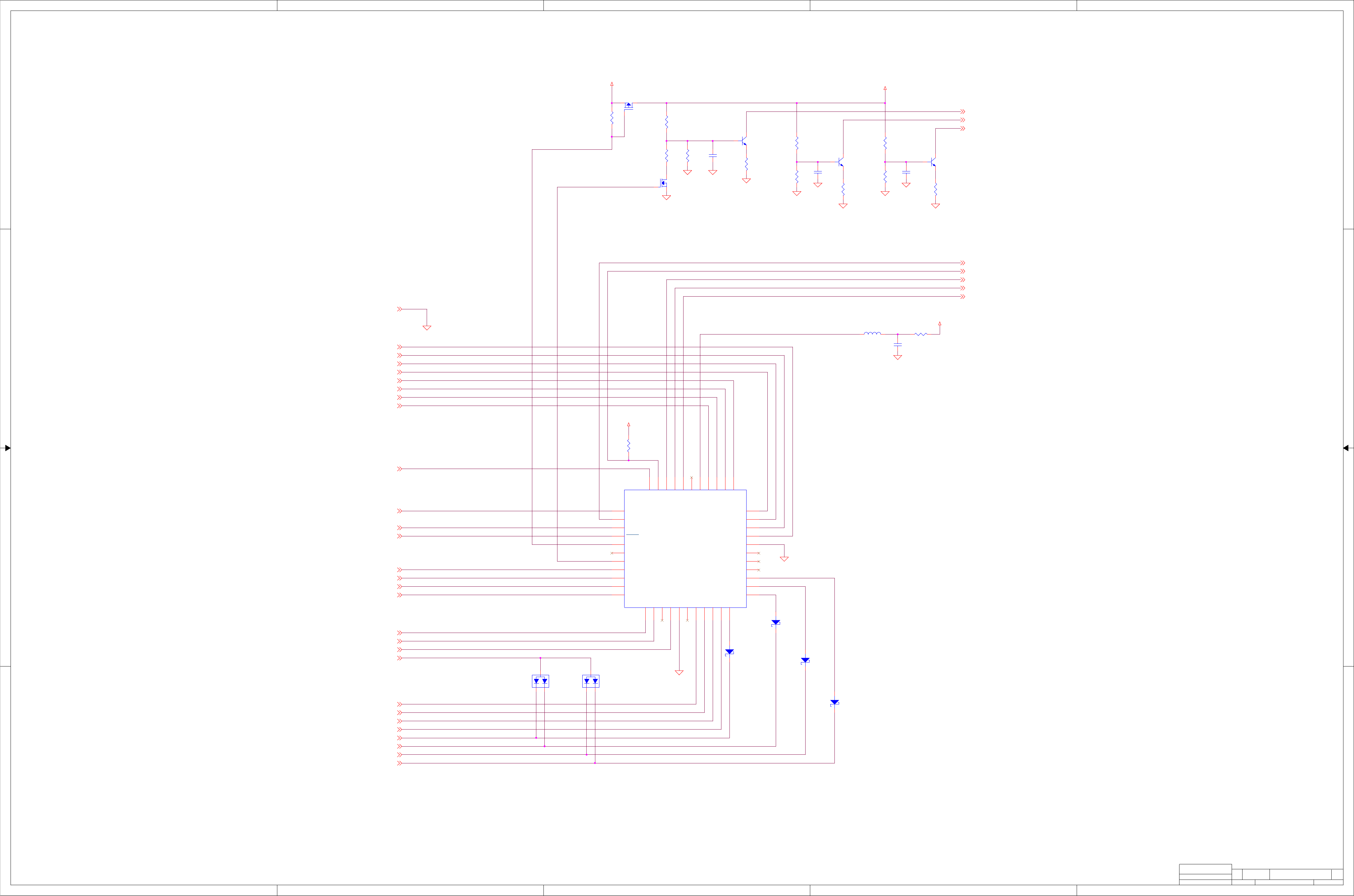
1
1
2
2
3
3
4
4
5
5
A A
B B
C C
D D
ATFVCC
/BK_DIM
ATMELVCC
/BK_ON
3V3LOGIC
3V3LED
3V3LOGIC
3V3LOGIC
VOL21
VOL31
VOL41
/RADON1,6
BL_LCD_N 1
BL_KP_N 1
BL_KNOB_N 1
/MINT 2
KIN51
KIN21
CHN41
AUX11
KOUT3 1
TOG11
CHN21
KIN31
AVRCLK5
/XRST1,2,3
KOUT2 1
TOG21
KIN41
MTXD1,5
MCLK1,5
/KPD_CS5
EMERGSW1
KIN61
CHN11
KIN11
SECSW1
AUX21
GND_SIGNAL1,2,3,4,5,6,8,9,10,11,12
MRXD 5
PTTSW1
KOUT1 1
CHN31
VOL11
AUX31
Scale
Rev
Sheet of
Size
CAGE Code Dwg No.
None
23386
Drawn
Thales Communications, Inc.
Rockville, Maryland
Thursday, November 15, 2001 7 12
024200716
E. HOOKER
D
Added GND to ICP.
Control Keypad
R414
100
1%
C410
0.01 uF
10%
R410
1K
1%
D40
CMDSH2-3
21
L69
BEAD
R411
1K
1%
R419
10
1%
D42
CMDSH2-3
21
C411
0.01 uF
10%
D45
CMDSH2-3
21
Q54
2N7002
1
32
R417
100
1%
R413
100K
1% Q52
MMBT3904
1
2 3
C412
0.01 uF
10%
R416
100K
1%
D44
CMPSH-3A
13
2
Q53
MMBT3904
1
2 3
AT90S8515
U43
AT90S8515-4AC
PB0 40
PB1 41
PB2 42
PB3 43
PB4 44
PA0 37
PA1 36
PA2 35
PA3 34
PA4 33
PA5 32
PA6 31
PA7 30
PC0
18
PC1
19
PC2
20
PC3
21
PC4
22
PC5 23
PC6 24
PC7 25
PD1
7
PD2
8
PD3
9
PD4
10
PD5
11
PD6
12
PD7
13
PB5
1
PB6
2
PB7
3
NC 39
NC 28
NC
17
NC
6
RESET
4
PD0
5
XTAL1
15
XTAL2
14
GND
16
ALE 27
OC1B 26
ICP 29
VCC 38
Q50
BSS84TA
1
32
D41
CMDSH2-3
21
R420
47.5K
1%
R415
100K
1%
Q51
MMBT3904
1
2 3
R418
100
1%
C413
0.1 uF
10%
R408
47.5K
1%
D43
CMPSH-3A
13
2
R412
1.5K
1%
R409
1K
1%
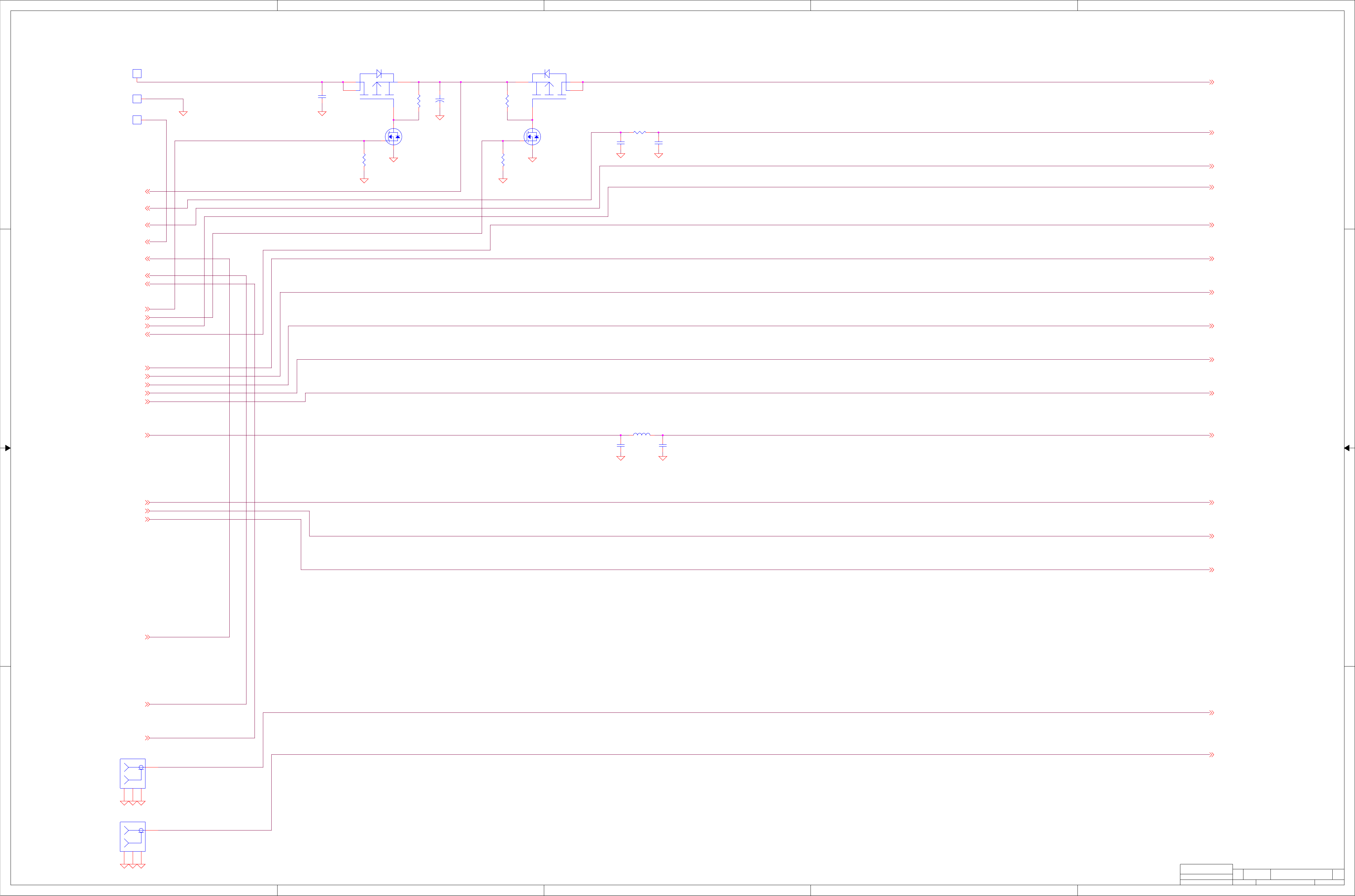
1
1
2
2
3
3
4
4
5
5
A A
B B
C C
D D
P54 P55
GND_SIGNAL 1,2,3,4,5,6,7,9,10,11,12
7.5VA_XCVR 11
PATEMP1,12
RSSI1,10
SYNTHLOCK1,11
TOPRF 12
SYNTHENA 2,11
SRENA 2,11
4.5VSW_XCVR 11,12
12DACENA 3,9
12DACCLK 1,9
12DACDATA 3,9
PROGCLK 2,9,11
PROGDATA 2,9,11
SIDERF 12
7.5VT1,6
GND_SIGNAL1,2,3,4,5,6,7,9,10,11,12
BATTSENSE1
PATEMP1,12
RSSI1,10
SYNTHLOCK1,11
BATTCTRL1
TXCTRL1
20VCLK1,11
PROGCLK2,9,11
PROGDATA2,9,11
SYNTHENA2,11
SRENA2,11
4.5VSW6
12DACENA3,9
12DACCLK1,9
12DACDATA3,9
8DACENA2,9
7.5VT_XCVR 12
20VCLK 1,11
EEPWP 1,9
8DACENA 2,9
EEPWP1,9
7.5VA1
Scale
Rev
Sheet of
Size
CAGE Code Dwg No.
None
23386
Drawn
Thales Communications, Inc.
Rockville, Maryland
Thursday, November 15, 2001 8 12
024200716
E. HOOKER
D
BATTCTRL TXCTRL
BATTERY+
BATTERY-
BATTSENSE
Transceiver Interface
E2
PAD1
1
U36-2
Si4925DY
32675
G
4
S
3D5
D6
E3
PAD1
1
E1
PAD1
1
C311
0.1 uF
10%
R299
150K
1%
R297
150K
1%
R298
150K
1%
R300
150K
1%
+
C312
15 uF
20%
20V
J2
OSMT
60165
1
2
3
4
Q47
2N7002LT1
SS-32550
1
32
J3
OSMT
60165
1
2
3
4
Q48
2N7002LT1
SS-32550
1
32
C318
0.1 uF
10%
R306
0
C319
0.1 uF
10%
U36-1
Si4925DY
32675
G
2
S1
D
7
D
8
C304
.22 uF
10
L66
1.2 uH
5%
C305
.22 uF
10
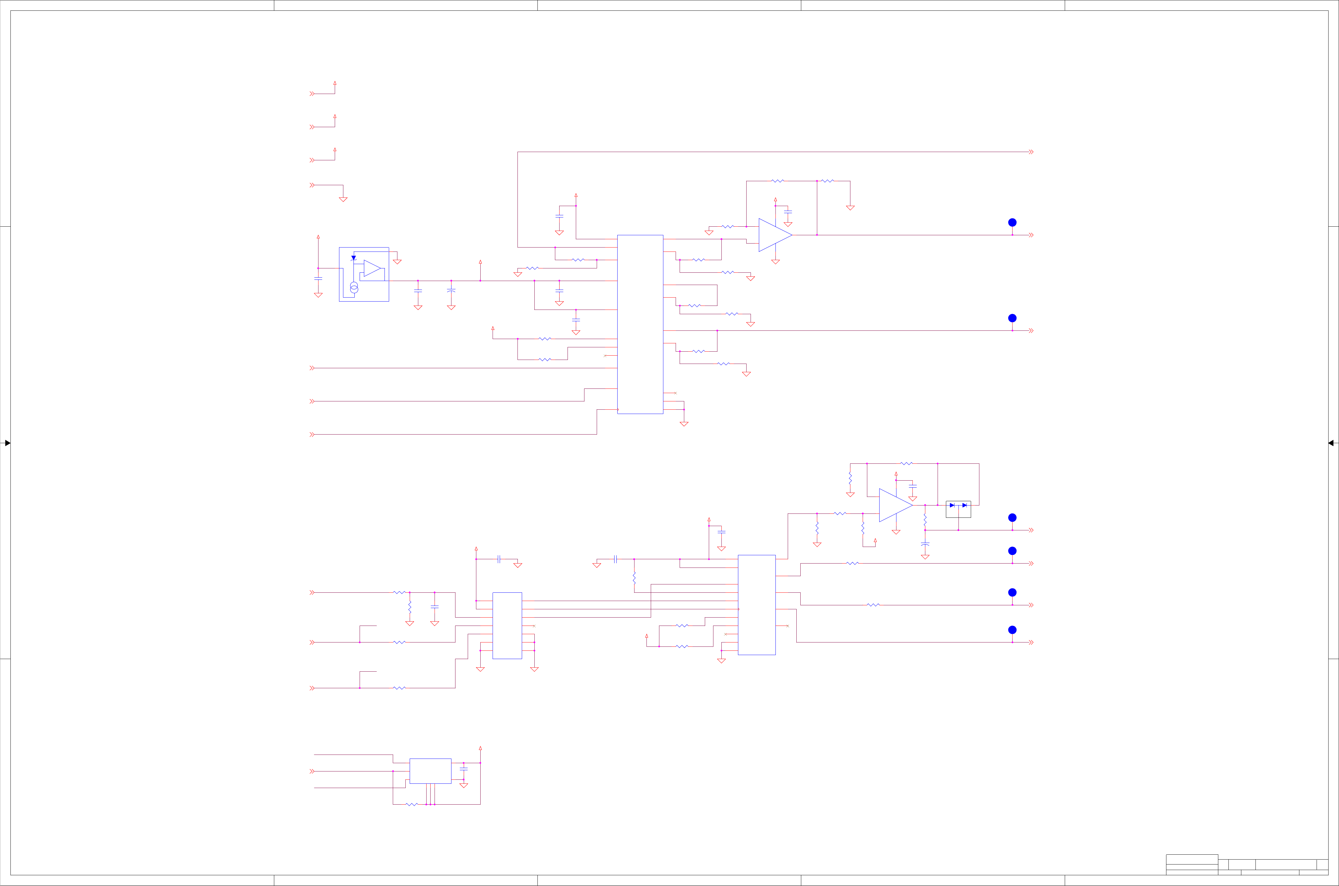
1
1
2
2
3
3
4
4
5
5
A A
B B
C C
D D
PROGCLK
PROGDATA
PROGCLK
PROGDATA
+5VDIG
+2.5VREF
+5VDIG
+5VDIG
+5VDIG
7.5VA_XCVR
+3.3VRX
+5VDIG
+5VDIG
+5VDIG
+2.5VREF
3V3LOGIC
20V
20V
+5VDIG11
GND_SIGNAL1,2,3,4,5,6,7,8,10,11,12
REFOSCMOD 11
IFAGC 10
7.5VA_XCVR8,11
+3.3VRX10,11
2ND_LO_TUNE 10
RXVTF 10
PWRSET 12
CTUNE 11
TXVCOMOD 11
12DACDATA3
12DACENA3
12DACCLK1
8DACENA2
PROGCLK2,11
PROGDATA2,11
EEPWP1
Scale
Rev
Sheet of
Size
CAGE Code Dwg No.
None
23386
Drawn
Thales Communications, Inc.
Rockville, Maryland
Thursday, November 15, 2001 9 12
024200716
E. HOOKER
D
8 BIT DAC
EEPROM
2.5 VDC
12 BIT DAC
Transceiver DACs
R175
130K
1%
R180
100K
1%
C275
0.1 uF
10%
R177
43.2K
1%
R272
100K
1%
R182
100K
1%
U33
MAX534B
365590
OUTB 1
OUTA 2
OUTC 16
OUTD 15
VDD
13
AGND
14
DGND
12
REF
3
DOUT 8
DIN
11
UPO
4
PDE
5
CLR*
7
LDAC
6
CS*
9
SCLK
10
R291
100
1%
R172
90.9K
1%
R290
100
1%
R252
100K
1%
C545
.033 uF
C257
0.1 uF
10%
R254
100K
1%
U76
LM7301
365661
OP 1
V-
2
-IP
4
+IP
3
V+ 5
R255
100K
1%
C269
0.1 uF
10%
C271
0.1 uF
10%
C544
.033 uF
U31
MAX525B
365588
OUTA 3
FBA 2
OUTB
4
FBB
5
OUTC 17
FBC 16
OUTD 18
FBD 19
AGND 1
DGND 11
DOUT 12
UPO
13
REFAB
6
REFCD
15
CS*
8
DIN
9
SCLK
10
VDD
20
CL*
7
PDL*
14
R258
100K
1%
C303
0.1 uF
10%
R259
100K
1%
C117
0.1 uF
10%
R86
100K
1%
C267
0.1 uF
10%
U15
24C64
365440
A0
1
A1
2
A2
3
GND 4
SDA
5
SCL
6
WP
7
VCC 8
R253
100K
1%
+
C206
1.0 uF
20%
35V
C276
0.1 uF
10%
R186
47.5K
1%
R273
100
1%
R169
274K
1%
U35
74HCT125
365078-125
4A
12
4OE*
13
1A
2
1OE* 1
2A
5
1Y 3
2Y 6
4Y 11
3OE* 10
3A
9
VCC
14
2OE* 4
GND
7
3Y 8
R287
1M
1%
R256
100K
1%
C279
1000 pF
5%
+
-
U32
AD1582C
SOT23/3P
365795
1
2
3
R257
100K
1%
R262
100K
1%
TP17
TP
1
R263
100K
1%
TP18
TP
1
TP19
TP
1
TP20
TP
1
TP21
TP
1
TP24
TP
1
+
C268
2.2 uF
10%
10V
SS-25131
D25
BAR43S
SS-35620
2
3
1
C270
0.1 uF
10%
R266
100K
1%
R264
100K
1%
R179
23.7K
1%
R181
NU
R196
10K
1%
R193
10K
1%
U75
LM7301
365661
OP 1
V-
2
-IP
4
+IP
3
V+ 5
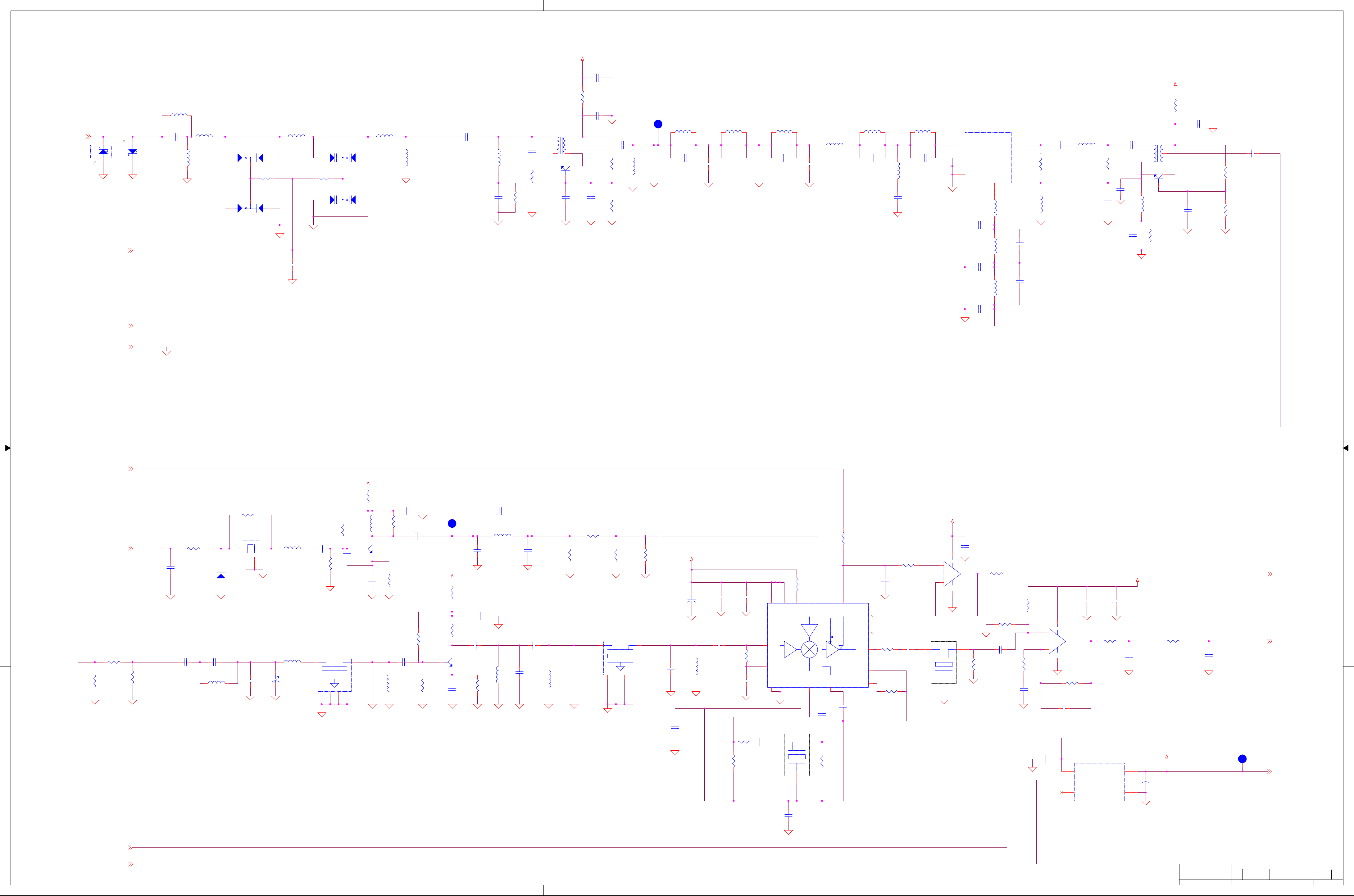
1
1
2
2
3
3
4
4
5
5
A A
B B
C C
D D
P3
P6
R2
R3 R5 R8 R9
P1
P11
R10 R11
R12
P2
R7
P5
P4
R6
P9
P10
R13
P12
P7
P8
R1
R4
+3.3VRX
+3.3VRX
+3.3VRX
+3.3VRX
+3.3VRX
+3.3VRX
+3.3VRX
+3.3VRX
RXVTF9
GND_SIGNAL1,2,3,4,5,6,7,8,9,11,12
RX_INPUT12
RSSI 1
IFOUT 3
2ND_LO_TUNE9
RXSINK12
IFAGC9
+3.3VRX 11
RXLO11
+3.3VRXEN11
Scale
Rev
Sheet of
Size
CAGE Code Dwg No.
None
23386
Drawn
Thales Communications, Inc.
Rockville, Maryland
Thursday, November 15, 2001 10 12
024200716
E. HOOKER
D
1T 4T
11T
136-174 MHZ
2 POLE BANDPASS FILTER
LOWPASS FILTER & IF NOTCH
MIXER
IF AMPLIFIER
1T 4T
11T
7T-AW
IF IC
2nd LO
RF
181-219MHz
AMPLIFIER
2nd IF AMPLIFIER
1st
2 dB PAD
Transceiver Receiver
PLACE NEAR FL3-3
PLACE C230 NEAR PIN 16, C536 NEAR PIN 20
PLACE NEAR U28-9
(VMID)
L62
0.82 uH
2%
R219
12.1K
1%
C28
27 pF
5%
C290
0.1 uF
10%
R229
2.21K
1%
L19
15 nH
2%
R225
681
1%
L20
33 nH
2%
C1
0.1 uF
10%
L63
150 nH
10%
R217
12.1K
1%
C30
18 pF
2%
C7
0.01 uF
10%
C289
91 pF
5%
R238
1.5K
1%
L21
39 nH
2%
C3
0.1 uF
10%
C293
12 pF
2%
R218
2.67K
1%
C31
10 pF
0.25pF
L7
0.39 uH
2%
L65
680 nH
10%
L64
1.0 uH
2%
C75
5.6 pF
0.25pF
C4
1000 pF
5%
R282
68.1
1%
R220
3.01K
1%
L15
5T-AW
3400439-3
C87
1.8 pF
0.25pF
C8
1.0 pF
0.1pF
R284
68.1
1%
C57
1.8 pF
0.25pF
C27
0.1 uF
10%
C2
0.1 uF
10%
R283
150
1%
L12
680 nH
10%
L18
6.8 uH
5%
C5
1000 pF
5%
C294
NU
C241
0.01 uF
10%
C29
NU
L1
56 nH
2%
C536
0.1 uF
10%
C227
56 pF
5%
Q2
MMBR901
32099
1
2 3
C9
2.7 pF
0.1pF
C222
0.1 uF
10%
R6
2.67K
1%
L3
56 nH
2%
C34
0.1 uF
10%
C223
18 pF
2%
R10
3.01K
1%
C11
5.6 pF
0.1pF
C292
4.7 uF
10%
10V
R212
18.2K
1%
R11
332
1%
L9
56 nH
2%
U4
LP2980A-3.3
365460
VOUT 5
ON/OFF
3
VIN
1
GND 2
NC
4
R213
1.3K
1%
R4
51.1
1%
L4
100 nH
2%
L2
47 nH
2%
R204
NU
R5
51.1
1%
C12
120 pF
5%
C10
9.1 pF
0.1pF
L24
1.2 uH
10%
L17
82 nH
2%
L5
100 nH
2%
C302
0.1 uF
10%
R31
200K
1%
C23
150 pF
5%
C13
120 pF
5%
C19
2-10 pF
SS-28058
12
C6
39 pF
5%
R208
NU
L10
330 nH
5%
C14
18 pF
2%
R251
51.1
1%
C15
22 pF
2%
C215
0.1 uF
10%
L11
1.2 uH
5%
C56
10 pF
0.25pF
L22
150 nH
2%
R276
51.1
1%
C21
NU
R571
49.9
1%
R33
1.82K
1%
R1
10
1%
L13
470 nH
10%
C547
NU
R2
10
1%
FL1
45 MHz 4-POLE
1600471-1
1 4
2
3
5
6
C224
0.1 uF
10%
R8
332
1%
C230
0.1 uF
10%
C242
39 pF
5%
R203
100
1%
C237
8.2 pF
.1pF
Y1
44.545 MHz
1600407-1
4 1
2
3
C244
0.1 uF
10%
+
C229
4.7 uF
10%
10V
C26
0.01 uF
10%
U1
EMRS-1A
84586
RF
4
GND
2
IF 5
GND
6
GND
3
LO
1
C550
0.1 uF
10%
D26
SMV1236-011
29037
2 1
C214
0.1 uF
10%
U28
AD607ARS
365513
RFHI
6
RFLO
5
MXOP
8
VMID
9
IFOP 14
RSSI 12
LOIP 4
IFHI
10
IFLO
11
VPS1 20
VPS2 16
PRUP 3
COM1
2
COM2
13
GREF 7
DMIP 15
IOUT 18
FDIN 1
FLTR 19
QOUT 17
C248
0.1 uF
10%
Q1
MMBR941
32098
1
2 3
R250
1.5K
1%
C246
0.1 uF
10%
C231
0.1 uF
10%
L6
3400439-5
NC
D1
MMBD701
SS-36034
1 3
2
C256
0.1 uF
10%
C240
0.1 uF
10%
C284
91 pF
5%
T1
136-174MHz
1600462-1
2 5
4
1 3
C247
3.3 pF
0.25pF
NC
D2
MMBD701
SS-36034
13
2
FL3
455 kHz
37121
2
3
1
C285
2.2 pF
.25pF
T2
45MHz
1600463-1
2 5
4
1 3
FL2
455 kHz
37107
2
3
1C236
NU
R280
20K
1%
L8
7T-AW
3400439-5
+
-
U29
OPA343
365701
1
V+
5
3
4
V-
2
C228
0.01 uF
10%
R281
20K
1%
R187
100K
1%
R222
49.9
1%
C225
0.1 uF
10%
C287
120 pF
5%
R9
100K
1%
SMV1204-136
D3
29050
3
21
R240
475
1%
L61
390 nH
10%
L25
100 nH
2%
R241
475
1%
L60
1.5 uH
2%
C61
120 pF
5%
R316
10
1%
C235
NU
SMV1204-136
D27
3
2 1
C286
3.3 pF
0.25pF
SMV1204-136
D28
3
2 1
C338
0.1 uF
10%
R230
332
1%
SMV1204-136
D4
3
21
C337
0.1 uF
10%
R12
51.1
1%
R215
10
1%
C18
8.2 pF
0.1pF
R206
10K
1%
R3
2.67K
1%
Q36
MMBR901
32099
1
2 3
R237
174
1%
C59
100 pF
5%
C22
0.1 uF
10%
C245
0.1 uF
10%
R236
1.3K
1%
Q35
MMBR901
32099
1
2 3
R7
3.01K
1%
C233
0.1 uF
10%
+
-
U27
LMC7101A
365438
1
V+
2
3
4
V-
5
C249
0.1 uF
10%
C226
56 pF
5%
C16
22 pF
2%
L14
5T-AW
3400439-3
R279
100
1%
R227
1.21K
1%
TP1
TP
1
C17
22 pF
2%
FL4
45 MHz 2-POLE
1600479-1
1 4
2
3
5
6
R224
1K
1%
TP2
TP
1
L16
1.8 uH
2%
C288
15 pF
2%
R214
1K
1%
TP3
TP
1
C25
6.2 pF
0.25pF
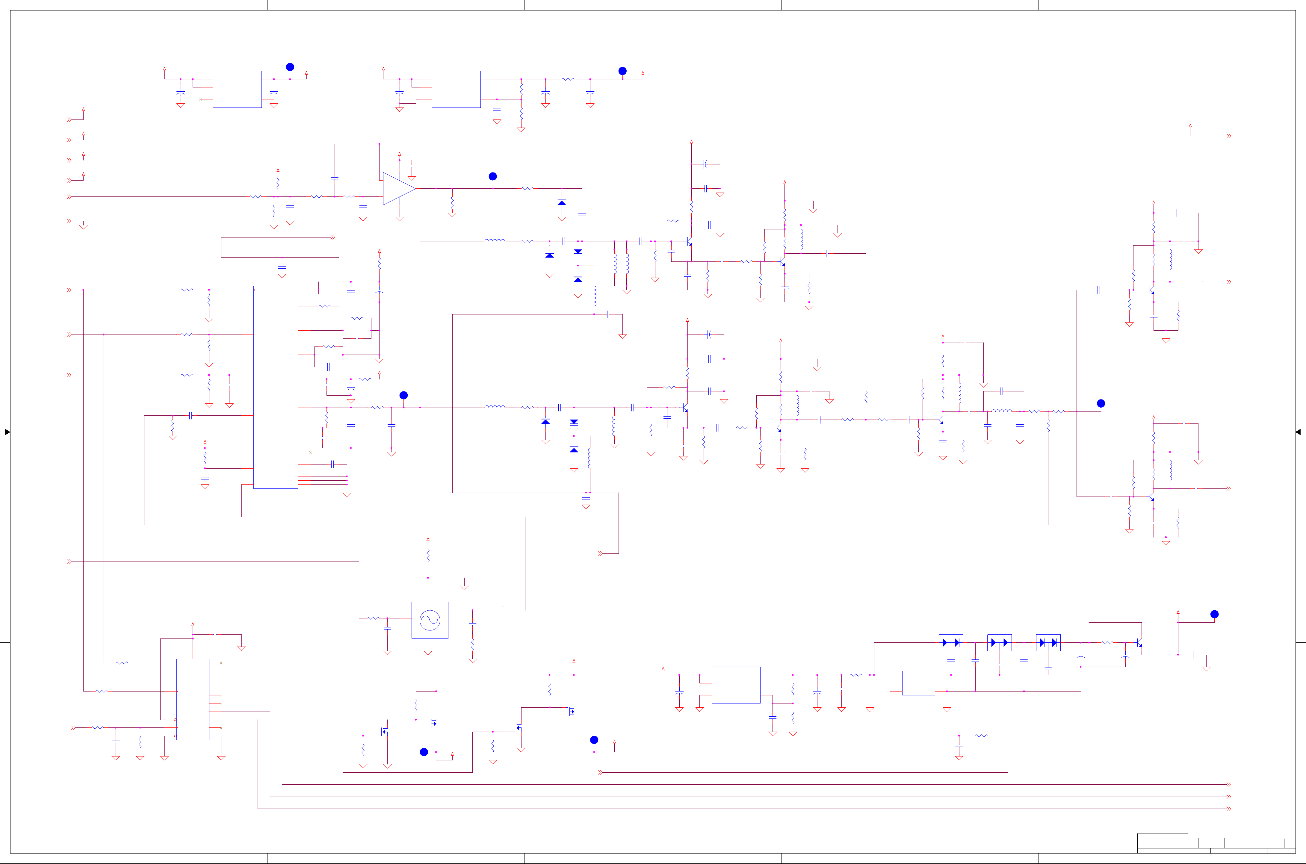
1
1
2
2
3
3
4
4
5
5
A A
B B
C C
D D
P20
R14
P18
R17
R18
R16
P26
P24
P25
P14
P13
P22
P15
P35
P34
P32
P33
P30
P31
P28
P29
R15
R19
P16
P36
R20
P17
P21
P27
P23
+3.3VDIG
+3.3VDIG
+3.3VRXS
+3.3VTXS
+3.3VTXS
+3.3VA
+3.3VA
+3.3VTXS
+3.3VA
+3.3VRXS
+3.3VTXS
4.5VSW_XCVR
+5VDIG
+3.3VDIG
7.5VA_XCVR
+5VDIG
+3.3VDIG
4.5VSW_XCVR
+3.3VRX
+5VDIG
7.5VA_XCVR
7.5VA_XCVR
+3.3VA
+3.3VRX
+3.3VTXS
20V
20V
+3.3VRXS
STD/SIDE 12
TX/RX 12
CTUNE9
REFOSCMOD9
SRENA2
+5VDIG 9
4.5VSW_XCVR8,12
+3.3VRX10
20VCLK1
PROGCLK2,9
SYNTHLOCK 1
+3.3VDIG12
RXLO 10
TXLO 12
GND_SIGNAL
1,2,3,4,5,6,7,8,
9,10,12
PROGDATA2,9
SYNTHENA2
TXVCOMOD9
7.5VA_XCVR8
+3.3VRXEN 10
Scale
Rev
Sheet of
Size
CAGE Code Dwg No.
None
23386
Drawn
Thales Communications, Inc.
Rockville, Maryland
Thursday, November 15, 2001 11 12
024200716
E. HOOKER
D
TX VCO
RX VCO
SYNTHESIZER
REF OSC
NC
VOLTAGE
MULTIPLIER
BUFFER
AMPLIFIER
+3.5V
6.00VDC
Note: Use single
point ground here
RX BUFFER
AMPLIFIER
TX BUFFER
AMPLIFIER
Transceiver Synthesizer
KEEP VERY SHORT
C301
1000 pF
5%
C159
1000 pF
5%
D18
BBY40
SS-29029
1 3
R288
1M
1%
R102
1K
1%
D15
BBY31
SS-29031
1 3
C167
15 pF
5%
R292
100
1%
R135
0
C175
15 pF
2%
R145
4.75K
1%
L52
27 nH
5%
2 1
C176
15 pF
2%
U20
MIC5205
365499
VOUT 5
ON/OFF
3
VIN
1
BYP 4
GND
2
R130
2.21K
1%
C154
1000 pF
5%
L51
1.5 uH
10%
1 2
R295
86.6K
1%
R149
332
1%
C150
1000 pF
5%
L50
68 nH
5%
12
+
C121
1.0 uF
20%
35V
R296
332K
1%
R124
47.5
1%
C141
0.1 uF
10%
R322
10K
1%
L47
1.5 uH
10%
12
C310
470 pF
10%
R146
10
1%
+
C124
4.7 uF
10%
10V
C145
1000 pF
5%
L43
82 nH
5%
12
C200
0.1 uF
10% D35
BAR43S
1
3
2
R150
5.62K
1%
C149
12 pF
2%
L44
1.5 uH
10%
1 2
C151
0.1 uF
10%
C308
.033 uF
10%
R137
4.32K
1%
L49
68 nH
5%
12
C546
.033 uF
C188
1000 pF
5%
C156
0.1 uF
10%
C309
.033 uF
10%
R136
182
1%
C178
0.1 uF
10%
L56
68 nH
5%
12
R159
121
1%
R152
511
1%
C168
1000 pF
5%
C182
1000 pF
5%
L48
56 nH
5%
12
C341
100 pF
C184
1000 pF
5%
R128
47.5
1%
C185
15 pF
5%
L55
1.5 uH
10%
1 2
C183
1000 pF
5%
R141
16.2
1%
C195
1000 pF
5%
L53
3400439-1
1 2
R92
7.5K
1%
C172
6800 pF
10%
22562-682
C307
.033 uF
10%
R142
16.2
1%
C53
10 pF
2%
C126
0.015 uF
10%
C177
0.068 uF
5%
C173
2200 pF
10%
R131
16.2
1%
R97
3.92K
1%
U77
LM7301
365661
OP 1
V-
2
-IP
4
+IP
3
V+ 5
C161
0.022 uF
10%
R105
4.75K
1%
R95
15K
1%
C146
0.022 uF
10%
R293
100
1%
R101
2.21K
1%
R153
22.1
1%
R109
332
1%
+
C143
4.7 uF
10V
10%
U24
74HC595
365459-595
SER
14
SRCLK
11
SRCLR
10
RCLK
12
G
13
QA 15
QB 1
QC 2
QD 3
QE 4
QF 5
QG 6
QH 7
QH' 9
VCC 16
GND 8
R106
22.1
1%
C140
1000 pF
5%
R107
10
1%
+
C123
4.7 uF
10%
10V
SS-25122-475-10
C160
1000 pF
5%
R99
47.5
1%
R183
1M
1%
C131
3300 pF
5%
R104
4.32K
1%
R116
10K
1%
R110
5.62K
1%
R143
51.1
1%
C135
8.2 pF
.1pF
R129
1M
1%
R103
182
1%
C165
10 pF
2%
R96
4.32K
1%
C539
NU
R114
1M
1%
R100
47.5
1%
C166
9.1 pF
.1pF
U19
SA7025DK
365423
CLK
1
DATA
2
STROBE
3
VSS 4
AUXIN 10
VSSA 12
RFIN
5
RFIN* 6
REFIN
8
VCCP
7
VDD 20
TEST 19
LOCK 18
RF 17
RN 16
VDDA 15
PHP 14
PHI 13
PHA 11
RA
9
C136
6.8 pF
.1pF
+
C162
4.7 uF
10V
10%
R566
NU
R94
182K
1%
C169
27 pF
5%
L46
100 nH
2%
12
Q34
BSS123
1
32
R112
511
1%
+
C120
4.7 uF
10%
10V
SS-25122-475-10
C180
18 pF
2%
D16
BBY40
13
Q33
BSS123
SS-32564
1
32
+
C152
2.2 uF
10%
10V
C187
1000 pF
5%
R147
3.01K
1%
L45
100 nH
2%
12
C155
0.1 uF
10%
R148
267
1%
R133
2.21K
1%
D19
SMV1493-011
29054
2 1
U21
MIC4416BM4
365621
VS
3
CTL
4GND 1
G2
C163
1000 pF
5%
R132
182
1%
Q32
Si2301DS
1
3 2
Q24
MMBR901
1
2 3
R185
47.5K
1%
R125
47.5
1%
C340
0.01 uF
C174
4.7 pF
.25pF
Q31
Si2301DS
32631
1
3 2
Q26
MMBR901
1
2 3
R98
23.7K
1%
R138
16.2
1%
C181
1000 pF
5%
U17
MIC5205
1%
365499
VOUT 5
ON/OFF
3
VIN
1
BYP 4
GND
2
Q21
MMBR901
32099
1
2 3
C158
0.1 uF
10%
C132
220 pF
5%
R139
16.2
1%
C295
0.01 uF
10%
Q22
MMBR901
1
2 3
C164
1000 pF
5%
R144
16.2
1%
+
C118
1.0 uF
20%
35V
25122-105-35-A
Q25
MMBR901
1
2 3
R120
1.3K
1%
R121
NU
C170
15 pF
5%
U16
LP2980A-5.0
365413
VOUT 5
ON/OFF
3
VIN
1
GND 2
NC
4
Q23
MMBR901
1
2 3
TP8
TP
1
C148
1000 pF
5%
R117
1.1K
1%
Q27
MMBR901
1
2 3
C191
0.01 uF
10%
R115
475
1%
TP9
TP
1
C137
22 pF
2%
C192
0.1 uF
10%
R89
110K
1%
C142
22 pF
2%
R111
10
1%
TP10
TP
1
R160
10
1%
R87
10
1%
R122
121
1%
C339
0.1 uF
TP11
TP
1
C139
4.7 pF
.25pF
R118
681
1%
+
C193
1.0 uF
20%
35V
C133
1000 pF
5%
R156
1.1K
1%
TP13
TP
1
R123
35.7K
1%
+
C190
2.2 uF
20%
16V
C128
0.1 uF
10%
R155
825
1%
TP12
TP 1
C202
.033 uF
10%
R113
100
1%
+
C125
2.2 uF
10%
10V
R157
100
1%
TP7
TP
1
C203
.033 uF
10%
R119
100
1%
TP14
TP
1
C129
0.1 uF
10%
R154
475
1%
D23
BAR43S
SS-35620
1
3
2
R126
100
1%
C134
1000 pF
5% R151
22.1
1%
D24
BAR43S
1
3
2
R140
22.1K
1%
R91
200K
1%
C138
22 pF
2%
C199
.033 uF
10%
R134
47.5K
1%
C130
1.0 pF
.1pF
R171
100K
1%
+
C201
1.0 uF
20%
35V
R127
22.1
1%
C144
1000 pF
5%
R178
1M
1%
R162
1K
1%
U42
12.8 MHz
37132
Vc
1
GND
2
OUT 3
Vcc
4
C186
1000 pF
5%
R173
100K
1%
Q46
MMBT3904
SS-32089-3904
1
2 3
R320
22.1
D20
SMV1207-001
13
C171
1000 pF
5%
+
C196
1.0 uF
20%
35V
D21
SMV1207-001
29036
1 3
C179
1000 pF
5%
R294
100
1%
C157
0.1 uF
10%
D17
SMV1213-001
29044
1 3
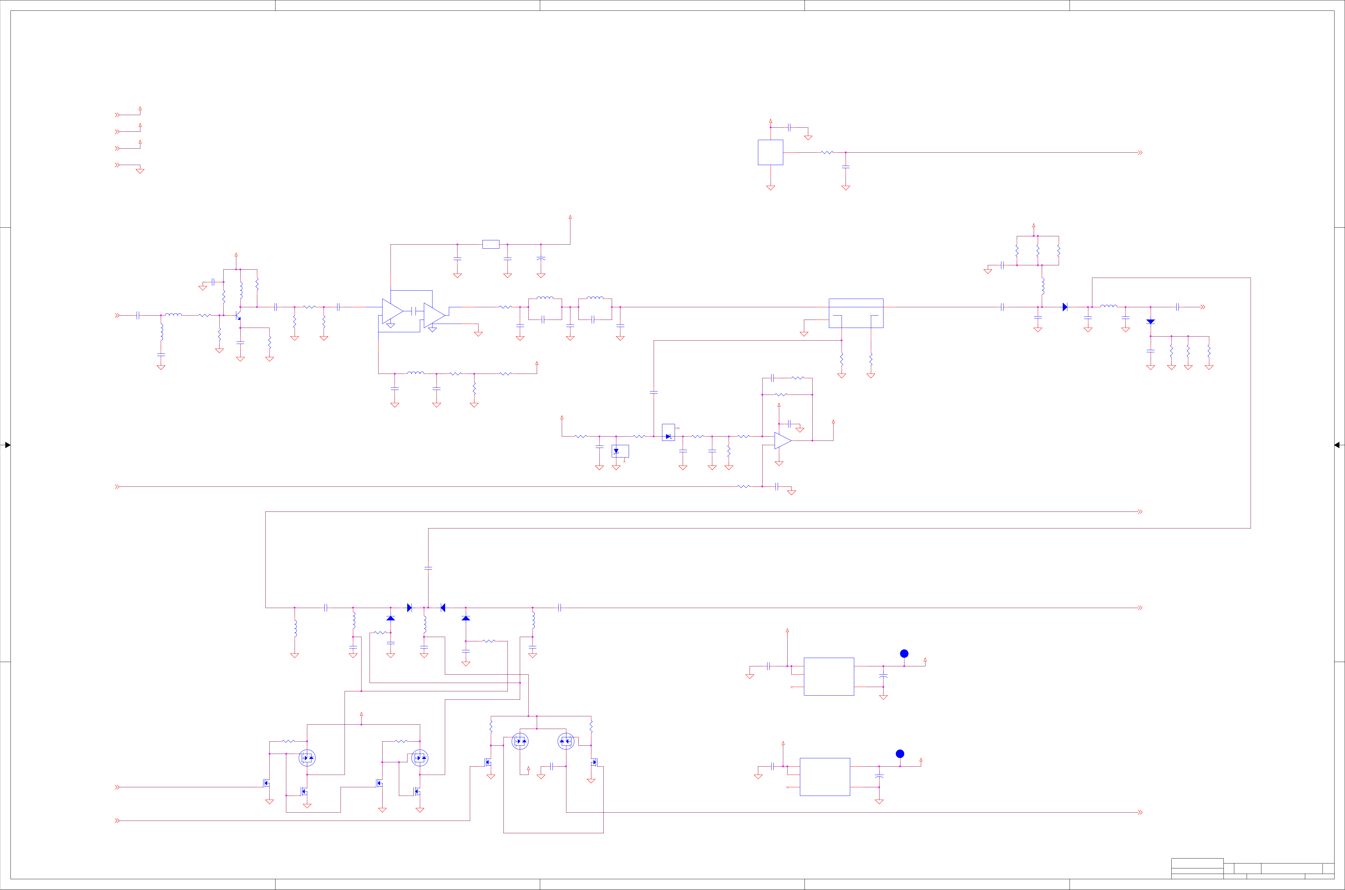
1
1
2
2
3
3
4
4
5
5
A A
B B
C C
D D
P38
R22R21 R23
P41P40
P43
P44
R29
P47 P49P45
R28
P46
P48
R30
R27
P42
P52
P53
P39
P50
R26R25
P51
R24
7.5VT_XCVR
+5VTX
+5VTX
VCONTROL
+5VTX
7.5VT_XCVR
TXSINK
4.5VSW_XCVR
TXSINK
4.5VSW_XCVR
+3.3VDIG
4.5VSW_XCVR
7.5VT_XCVR
VCONTROL
+3.3VDIG
7.5VT_XCVR
7.5VT_XCVR
TXLO11
PATEMP 1
7.5VT_XCVR8
TX/RX11
RXSINK 10
SIDERF 8
RX_INPUT 10
4.5VSW_XCVR8,11
PWRSET9
GND_SIGNAL1,2,3,4,5,6,7,8,9,10,11
+3.3VDIG11
TOPRF 8
STD/SIDE11
Scale
Rev
Sheet of
Size
CAGE Code Dwg No.
None
23386
Drawn
Thales Communications, Inc.
Rockville, Maryland
Thursday, November 15, 2001 12 12
024200716
E. HOOKER
D
(FROM SYNTH)
PRE-DRIVER POWER MODULE
SENSOR LOCATED CLOSE
TO POWER MODULE
DETECTOR / POWER
CONTROL
TX/RX PIN
SWITCH
ANTENNA PIN
SWITCH
2 dB attenuator
Transceiver Transmitter
R74
100K
1%
L35
180 nH
5% C114
10 pF
2%
R69
1K
1%
L37
100 nH
2%
L41
1.2 uH
2%
+
C108
4.7 uF
10%
10V
SS-25122-475-10
C86
15 pF
5%
R82
100K
D13
MA4P7001F
36047
2 1
R47
562
1%
L40
1.2 uH
2%
D14
MA4P7001F
36047
21
Q7
MMBR941
32098
1
2 3
Q14
BSS123
1
32
L80
NU
5%
D7
MA4P7001F
2 1
C83
10 pF
2%
Q16
BSS123
1
32
D8
MA4P7001F
36047
21
L30
6T#24-AW
3400439-9
C94
1000 pF
5%
D10
MA4P7001F
2 1
L31
5T#24-AW
3400439-10
C97
1000 pF
5%
D9
MA4P7001F
2 1
C84
6.8 pF
.25pF
C74
0.01 uF
10%
R73
1.82K
1%
C92
0.01 uF
10%
C98
1000 pF
5%
TP5
TP
1
R57
150
1%
R72
1.82K
1%
R319
0
TP6
TP
1
R55
1.3K
1%
L38
1.2 uH
2%
R52
475
1%
Q15
BSS123
SS-32564
1
32
U14
LP2980A-5.0
365413
VOUT 5
ON/OFF
3
4
4
VIN
1
GND 2
C216
0.1 uF
10%
C540
1000 pF
5%
Q18
BSS123
1
32
L28
120 nH
10%
R191
100
1%
R79
100K
1%
R49
10
1%
R81
100K
R44
475
1%
C78
1000 pF
5%
Q17
BSS123
1
32
Q19
BSS123
1
32
NC
D12
HSMS-2800
SS-35616
13
2
R80
100K
1%
NC
D11
HSMS-2800
SS-35616
1 3
2
C331
0.018 uF
10%
C104
390 pF
5%
+
C328
3.3 uF
10%
16V
C306
0.1 uF
C335
0.018 uF
10%
C103
390 pF
5%
L68
0.22 uH
10%
L39
1.2 uH
2%
C334
0.1 uF
10%
C109
0.1 uF
10%
R315
562
1%
C38
0.1 uF
10%
C82
22 pF
2%
C107
1000 pF
5%
C81
2.7 pF
.25pF
U3
LP2980A-3.3
365460
VOUT 5
ON/OFF
3
4
4
VIN
1
GND 2
L42
6T-AW
3400439-11
U11
LM50B
365437
GND
3+V 1
OUT 2
+
C43
4.7 uF
10%
10V
SS-25122-475-10
R66
51.1
1%
RF IN
VGG
VDD
RF OUT
U37
M68776-E01
84604
1
2
3
4
5
R68
100K
1%
C332
0.018 uF
10%
R67
51.1
1%
B1
50@100
45270
Q10
Si2301DS
32631
1
3 2
C95
3300 pF
5%
C100
1000 pF
5%
Q12
Si2301DS
32631
1
3 2
R71
20K
1%
U12
20 dB Coupler
1600458-1
3 1
5
2
4
Q13
Si2301DS
32631
1
3 2
+
-
U13
LMC7101A
365438
3
41
5 2
R78
47.5
1%
Q11
Si2301DS
32631
1
3 2
R85
47.5
1%
1/10W
C110
0.01 uF
10%
C127
1.5 pF
.1pF
R75
2.21K
1%
R84
43.2
1%
R64
0
R77
43.2
1%
R70
1K
1%
R83
43.2
1%
C106
1000 pF
5%
R76
43.2
1%
C105
1000 pF
5%
C111
1000 pF
5%
C96
1000 pF
5%
C209
6.8 pF
.25pF
R65
NU
C88
0.01 uF
10%
C115
10 pF
2%
R558
562
1%
C102
1000 pF
5%
C77
10 pF
2%
C113
1000 pF
5%
R557
562
1%
C101
1000 pF
5%
R48
2K
1%
C112
1000 pF
5%
C336
0.01 uF
10%
R51
51.1
1%
C116
1000 pF
5%