Dialog Semiconductor DA14580REFA DA14580 Antenna module for QFN48 package with Bluetooth Low Energy User Manual UM B 036 DA14580 Antenna Module QFN48 rev2 0
Dialog Semiconductor BV DA14580 Antenna module for QFN48 package with Bluetooth Low Energy UM B 036 DA14580 Antenna Module QFN48 rev2 0
User Manual
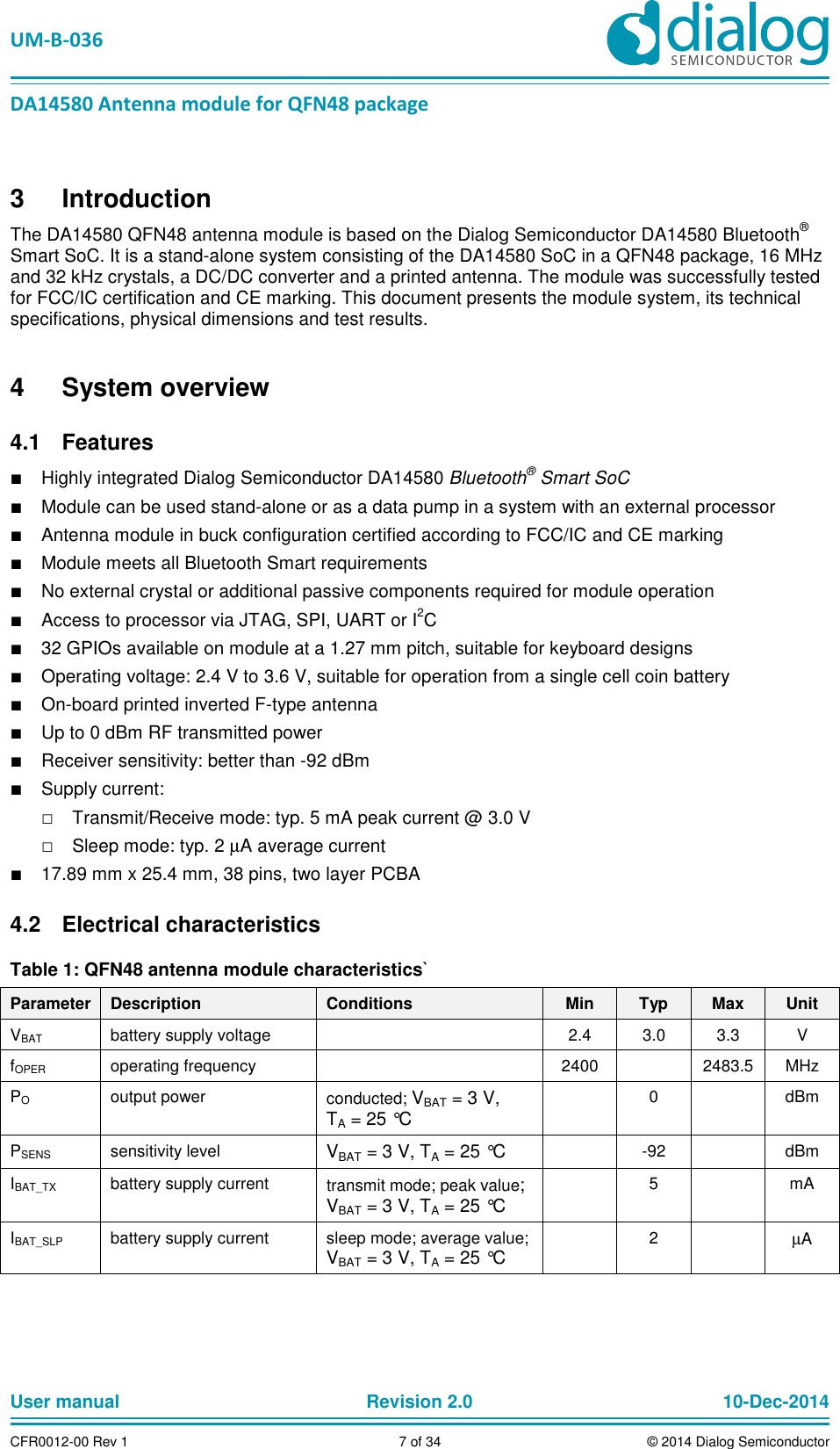
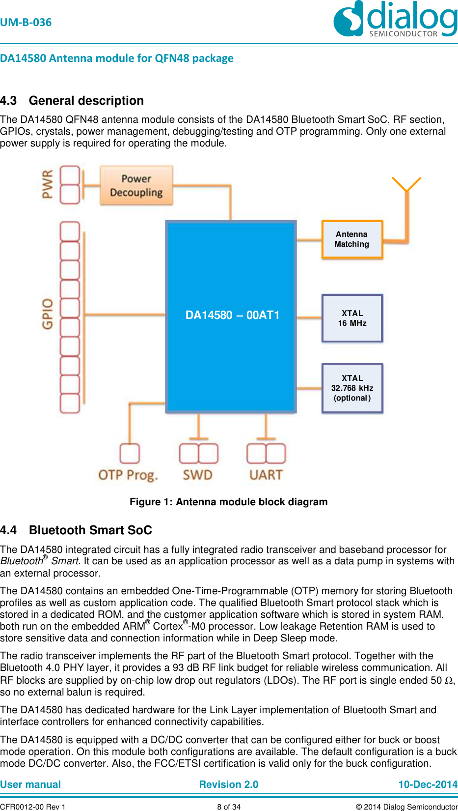
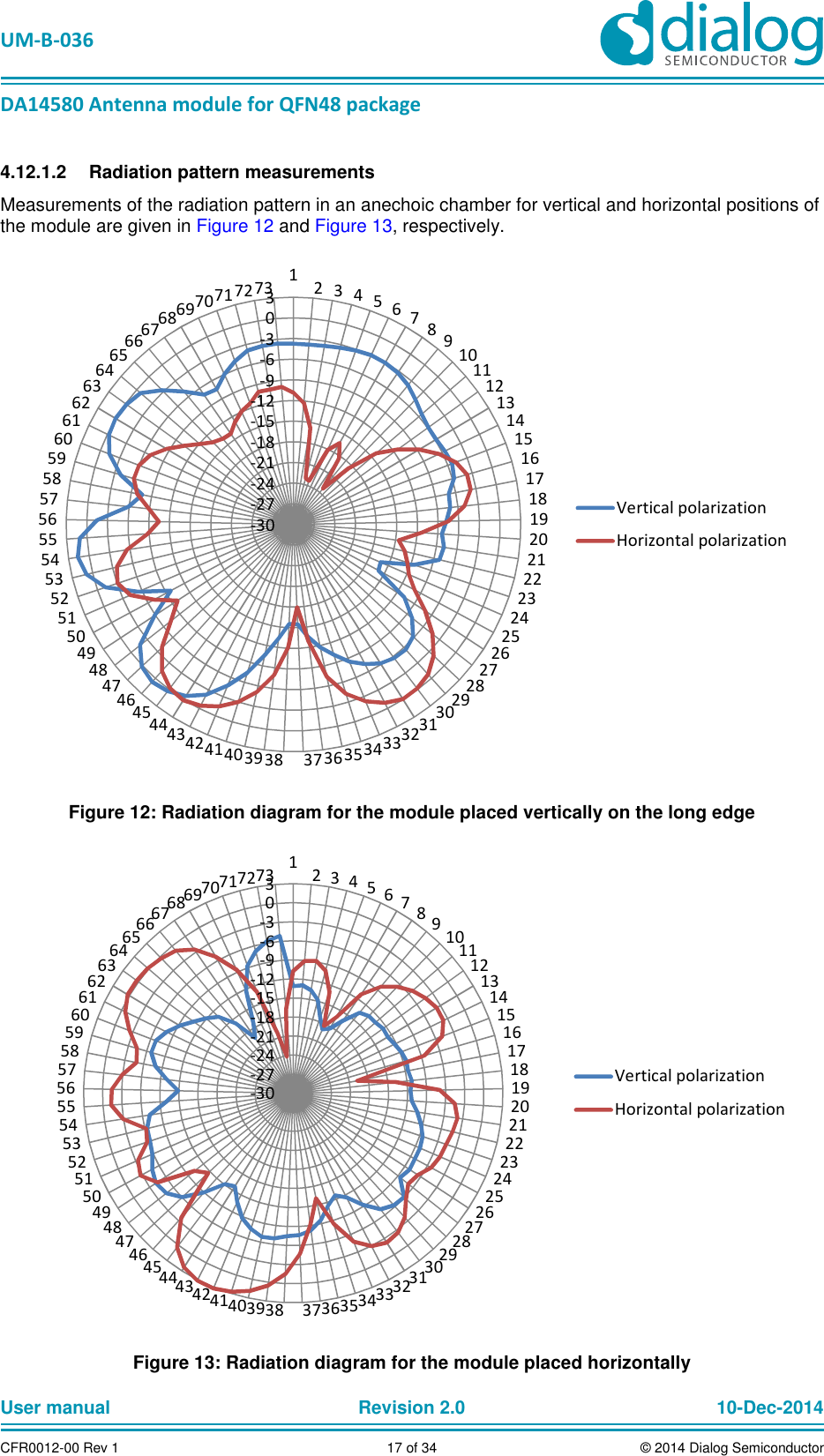
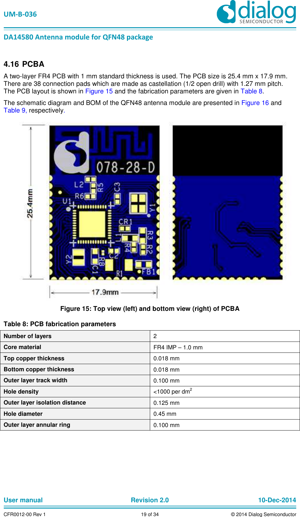
![UM-B-036 DA14580 Antenna module for QFN48 package User manual Revision 2.0 10-Dec-2014CFR0012-00 Rev 1 18 of 34 © 2014 Dialog Semiconductor Tuning the 16 MHz crystal 4.13The accuracy of the 16 MHz crystal (±10ppm) guarantees the ‘in spec’ operation of the QFN48 antenna module. However, further trimming of the 16 MHz crystal is possible using the procedure that is described in AN-B-020 End product testing and programming guidelines. See Ref.[2]. Software 4.14The standard SDK release software, without modifications, can be used for testing or operating the QFN48 antenna module. Test platform 4.15An interposer (078-46-A) was built for hardware interfacing the Expert DK Motherboard (580-MB-vC2 / 078-10-C2) to the QFN48 antenna module. The interposer can be used as a stand-alone platform, as it has a debug port (J39). The debug port consist of JTAG, UART, VPP, VBAT and GND signals. Figure 14: Interposer (078-46-A) for the QFN48 antenna module](https://usermanual.wiki/Dialog-Semiconductor/DA14580REFA/User-Guide-2514497-Page-18.png)