Dialog Semiconductor DA14580REFA DA14580 Antenna module for QFN48 package with Bluetooth Low Energy User Manual UM B 036 DA14580 Antenna Module QFN48 rev2 0
Dialog Semiconductor BV DA14580 Antenna module for QFN48 package with Bluetooth Low Energy UM B 036 DA14580 Antenna Module QFN48 rev2 0
User Manual

User manual
DA14580 Antenna module for
QFN48 package
UM-B-036
Abstract
This document describes the Bluetooth® Smart antenna module, based on the DA14580 SoC.
Target hardware: da14580_rd_module_qfn48_vD, board number: 078-28-D.

UM-B-036
DA14580 Antenna module for QFN48 package
User manual
Revision 2.0
10
-
Dec
-
2014
CFR0012-00 Rev 1 2 of 34 © 2014
Dialog Semiconductor
Contents
Contents .................................................................................................................................... 2
Figures ....................................................................................................................................... 4
Tables ........................................................................................................................................ 4
1 Terms and definitions ........................................................................................................... 6
2 References ........................................................................................................................... 6
3 Introduction ......................................................................................................................... 7
4 System overview .................................................................................................................. 7
Features ................................................................................................................................ 7
4.1
Electrical characteristics ....................................................................................................... 7
4.2
General description............................................................................................................... 8
4.3
Bluetooth Smart SoC ............................................................................................................. 8
4.4
Schematic diagram ................................................................................................................ 9
4.5
Module pinout .................................................................................................................... 10
4.6
Module GPIOs ..................................................................................................................... 11
4.7
Reset ..................................................................................................................... 11
4.7.1
Power management ............................................................................................................ 12
4.8
DC/DC converter in boost configuration .............................................................. 13
4.8.1
Crystals ................................................................................................................................ 13
4.9
OTP programming ............................................................................................................... 14
4.10
Debugging/testing ports ..................................................................................................... 14
4.11
RF section ............................................................................................................................ 14
4.12
Antenna ................................................................................................................ 14
4.12.1
4.12.1.1 Radiation diagrams ............................................................................ 16
4.12.1.2 Radiation pattern measurements ...................................................... 17
Tuning the 16 MHz crystal .................................................................................................. 18
4.13
Software .............................................................................................................................. 18
4.14
Test platform....................................................................................................................... 18
4.15

UM-B-036
DA14580 Antenna module for QFN48 package
User manual
Revision 2.0
10
-
Dec
-
2014
CFR0012-00 Rev 1 3 of 34 © 2014
Dialog Semiconductor
PCBA .................................................................................................................................... 19
4.16
5 Measurements ....................................................................................................................22
Receiver sensitivity (conducted) ......................................................................................... 22
5.1
Test description .................................................................................................... 22
5.1.1
Test setup ............................................................................................................. 22
5.1.2
Test results ........................................................................................................... 22
5.1.3
Transmitter output power (conducted) .............................................................................. 24
5.2
Test description .................................................................................................... 24
5.2.1
Test setup ............................................................................................................. 24
5.2.2
Test results ........................................................................................................... 24
5.2.3
Current consumption .......................................................................................................... 24
5.3
Test setup ............................................................................................................. 24
5.3.1
Test results ........................................................................................................... 25
5.3.2
6 FCC/IC Certification and CE marking .....................................................................................27
Standards and conformity assessment ............................................................................... 27
6.1
FCC requirements regarding the end product and end user .............................................. 28
6.2
End product marking ............................................................................................ 28
6.2.1
End product literature .......................................................................................... 28
6.2.2
Industry Canada requirements regarding the end product and end user .......................... 29
6.3
End product marking ............................................................................................ 29
6.3.1
End product literature .......................................................................................... 29
6.3.2
1999/5/EC Directive ............................................................................................................ 29
6.4
RoHS compliance .................................................................................................. 32
6.4.1
7 Revision history ...................................................................................................................33

UM-B-036
DA14580 Antenna module for QFN48 package
User manual
Revision 2.0
10
-
Dec
-
2014
CFR0012-00 Rev 1 4 of 34 © 2014
Dialog Semiconductor
Figures
Figure 1: Antenna module block diagram ............................................................................................. 8
Figure 2: Schematic diagram of the DA14580 QFN48 antenna module ............................................... 9
Figure 3: Module pin locations ............................................................................................................ 10
Figure 4: Power management, DC/DC converter in buck configuration ............................................. 12
Figure 5: Current consumption during an Advertising frame ............................................................. 12
Figure 6: DA14580 DC/DC converter circuit ........................................................................................ 13
Figure 7: RF section: PCB layout (left) and schematic (right) .............................................................. 14
Figure 8: Antenna geometry ............................................................................................................... 15
Figure 9: Matching network: R5 (5.1 nH) and R6 (3.9 nH) .................................................................. 15
Figure 10: Antenna VSWR measurements .......................................................................................... 16
Figure 11: Far field antenna directivity @ 2.44 GHz ........................................................................... 16
Figure 12: Radiation diagram for the module placed vertically on the long edge .............................. 17
Figure 13: Radiation diagram for the module placed horizontally ..................................................... 17
Figure 14: Interposer (078-46-A) for the QFN48 antenna module ..................................................... 18
Figure 15: Top view (left) and bottom view (right) of PCBA ............................................................... 19
Figure 16: Schematic of the DA14580 QFN48 antenna module ......................................................... 20
Figure 17: Test setup for the conducted RF measurements ............................................................... 22
Figure 18: Conducted output power per channel ............................................................................... 24
Figure 19: Supply current during an Advertising frame ...................................................................... 25
Figure 20: Supply current during periodic transmissions every 700 ms ............................................. 25
Figure 21: Supply current during Extended Sleep mode ..................................................................... 26
Tables
Table 1: QFN48 antenna module characteristics .................................................................................. 7
Table 2: Module pin assignment (top view) ........................................................................................ 10

UM-B-036
DA14580 Antenna module for QFN48 package
User manual
Revision 2.0
10
-
Dec
-
2014
CFR0012-00 Rev 1 5 of 34 © 2014
Dialog Semiconductor
Table 3: GPIO pins: available functions ............................................................................................... 11
Table 4: DA14580 DC/DC converter configurations ............................................................................ 13
Table 5: Crystal characteristics ............................................................................................................ 14
Table 6: QFN48 antenna module debug ports .................................................................................... 14
Table 7: Far field antenna parameters @ 2.44 GHz ............................................................................ 16
Table 8: PCB fabrication parameters ................................................................................................... 19
Table 9: Bill of Materials ...................................................................................................................... 21
Table 10: Conducted receiver sensitivity ............................................................................................ 23
Table 11: Peak current during Advertising mode ................................................................................ 25
Table 12: Average current in Extended Sleep mode ........................................................................... 26

UM-B-036
DA14580 Antenna module for QFN48 package
User manual
Revision 2.0
10
-
Dec
-
2014
CFR0012-00 Rev 1 6 of 34 © 2014
Dialog Semiconductor
1 Terms and definitions
BLE Bluetooth Low Energy (now: Bluetooth Smart)
BOM Bill Of Materials
DUT Device Under Test
ERP Effective Radiated Power
GPIO General Purpose Input/Output
PCBA Printed Circuit Board Assembled
PCB Printed Circuit Board
RF Radio Frequency
Rx Receive
SoC System on Chip
Tx Transmit
VSWR Voltage Standing Wave Ratio
2 References
1. DA14580 Low Power Bluetooth Smart SoC, Datasheet, Dialog Semiconductor
2. AN-B-020: End product testing and programming guidelines, Application note, Dialog
Semiconductor

UM-B-036
DA14580 Antenna module for QFN48 package
User manual
Revision 2.0
10
-
Dec
-
2014
CFR0012-00 Rev 1 7 of 34 © 2014
Dialog Semiconductor
3 Introduction
The DA14580 QFN48 antenna module is based on the Dialog Semiconductor DA14580 Bluetooth
®
Smart SoC. It is a stand-alone system consisting of the DA14580 SoC in a QFN48 package, 16 MHz
and 32 kHz crystals, a DC/DC converter and a printed antenna. The module was successfully tested
for FCC/IC certification and CE marking. This document presents the module system, its technical
specifications, physical dimensions and test results.
4 System overview
Features
4.1
■
Highly integrated Dialog Semiconductor DA14580 Bluetooth
®
Smart SoC
■
Module can be used stand-alone or as a data pump in a system with an external processor
■
Antenna module in buck configuration certified according to FCC/IC and CE marking
■
Module meets all Bluetooth Smart requirements
■
No external crystal or additional passive components required for module operation
■
Access to processor via JTAG, SPI, UART or I
2
C
■
32 GPIOs available on module at a 1.27 mm pitch, suitable for keyboard designs
■
Operating voltage: 2.4 V to 3.6 V, suitable for operation from a single cell coin battery
■
On-board printed inverted F-type antenna
■
Up to 0 dBm RF transmitted power
■
Receiver sensitivity: better than -92 dBm
■
Supply current:
□
Transmit/Receive mode: typ. 5 mA peak current @ 3.0 V
□
Sleep mode: typ. 2 µA average current
■
17.89 mm x 25.4 mm, 38 pins, two layer PCBA
Electrical characteristics
4.2
Table 1: QFN48 antenna module characteristics`
Parameter Description Conditions Min Typ Max Unit
V
BAT
battery supply voltage 2.4 3.0 3.3 V
f
OPER
operating frequency 2400 2483.5 MHz
P
O
output power conducted;
V
BAT
= 3 V,
T
A
= 25 °C
0 dBm
P
SENS
sensitivity level
V
BAT
= 3 V, T
A
= 25 °C
-92 dBm
I
BAT_TX
battery supply current transmit mode; peak value
;
V
BAT
= 3 V, T
A
= 25 °C
5 mA
I
BAT_SLP
battery supply current sleep mode; average value;
V
BAT
= 3 V, T
A
= 25 °C
2 µA
UM-B-036
DA14580 Antenna module for QFN48 package
User manual
Revision 2.0
10
-
Dec
-
2014
CFR0012-00 Rev 1 8 of 34 © 2014
Dialog Semiconductor
General description
4.3
The DA14580 QFN48 antenna module consists of the DA14580 Bluetooth Smart SoC, RF section,
GPIOs, crystals, power management, debugging/testing and OTP programming. Only one external
power supply is required for operating the module.
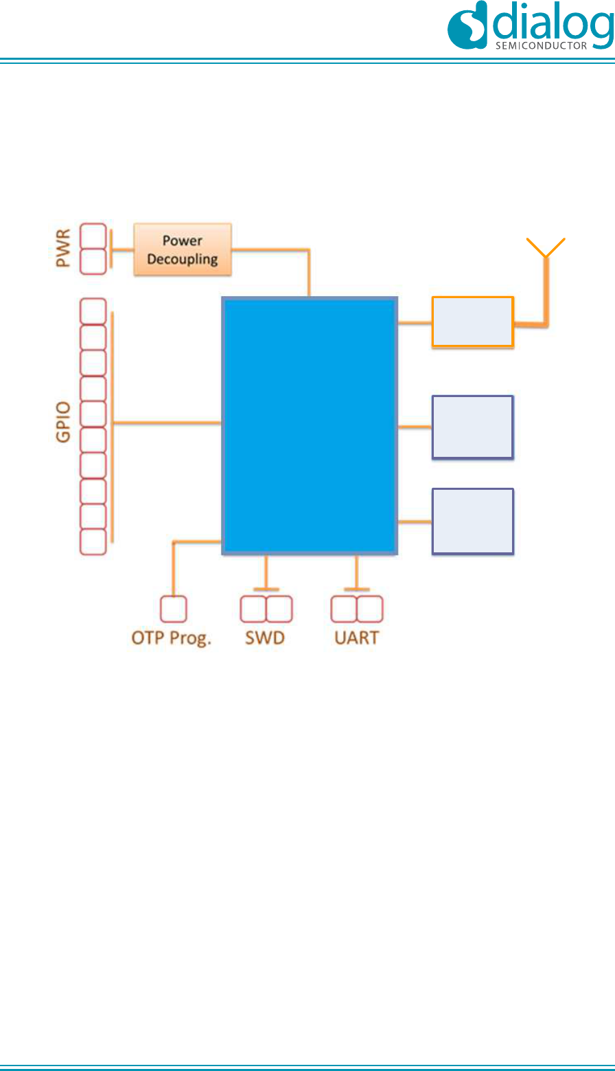
DA14580 – 00AT1
XTAL
32.768 kHz
(optional)
XTAL
16 MHz
Antenna
Matching
Figure 1: Antenna module block diagram
Bluetooth Smart SoC
4.4
The DA14580 integrated circuit has a fully integrated radio transceiver and baseband processor for
Bluetooth
®
Smart. It can be used as an application processor as well as a data pump in systems with
an external processor.
The DA14580 contains an embedded One-Time-Programmable (OTP) memory for storing Bluetooth
profiles as well as custom application code. The qualified Bluetooth Smart protocol stack which is
stored in a dedicated ROM, and the customer application software which is stored in system RAM,
both run on the embedded ARM
®
Cortex
®
-M0 processor. Low leakage Retention RAM is used to
store sensitive data and connection information while in Deep Sleep mode.
The radio transceiver implements the RF part of the Bluetooth Smart protocol. Together with the
Bluetooth 4.0 PHY layer, it provides a 93 dB RF link budget for reliable wireless communication. All
RF blocks are supplied by on-chip low drop out regulators (LDOs). The RF port is single ended 50 Ω,
so no external balun is required.
The DA14580 has dedicated hardware for the Link Layer implementation of Bluetooth Smart and
interface controllers for enhanced connectivity capabilities.
The DA14580 is equipped with a DC/DC converter that can be configured either for buck or boost
mode operation. On this module both configurations are available. The default configuration is a buck
mode DC/DC converter. Also, the FCC/ETSI certification is valid only for the buck configuration.
UM-B-036
DA14580 Antenna module for QFN48 package
User manual
Revision 2.0
10
-
Dec
-
2014
CFR0012-00 Rev 1 9 of 34 © 2014
Dialog Semiconductor
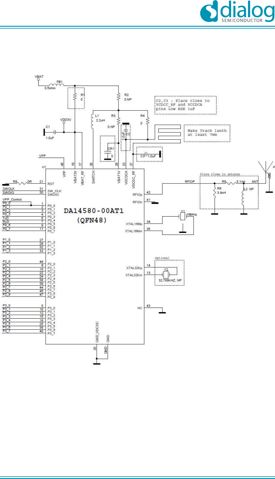
Schematic diagram
4.5
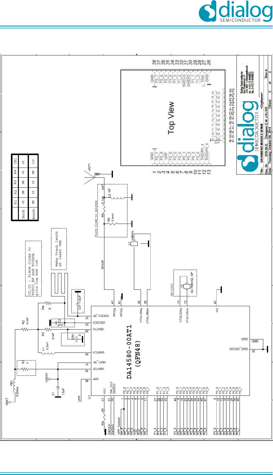
Figure 2: Schematic diagram of the DA14580 QFN48 antenna module
UM-B-036
DA14580 Antenna module for QFN48 package
User manual
Revision 2.0
10
-
Dec
-
2014
CFR0012-00 Rev 1 10 of 34 © 2014
Dialog Semiconductor
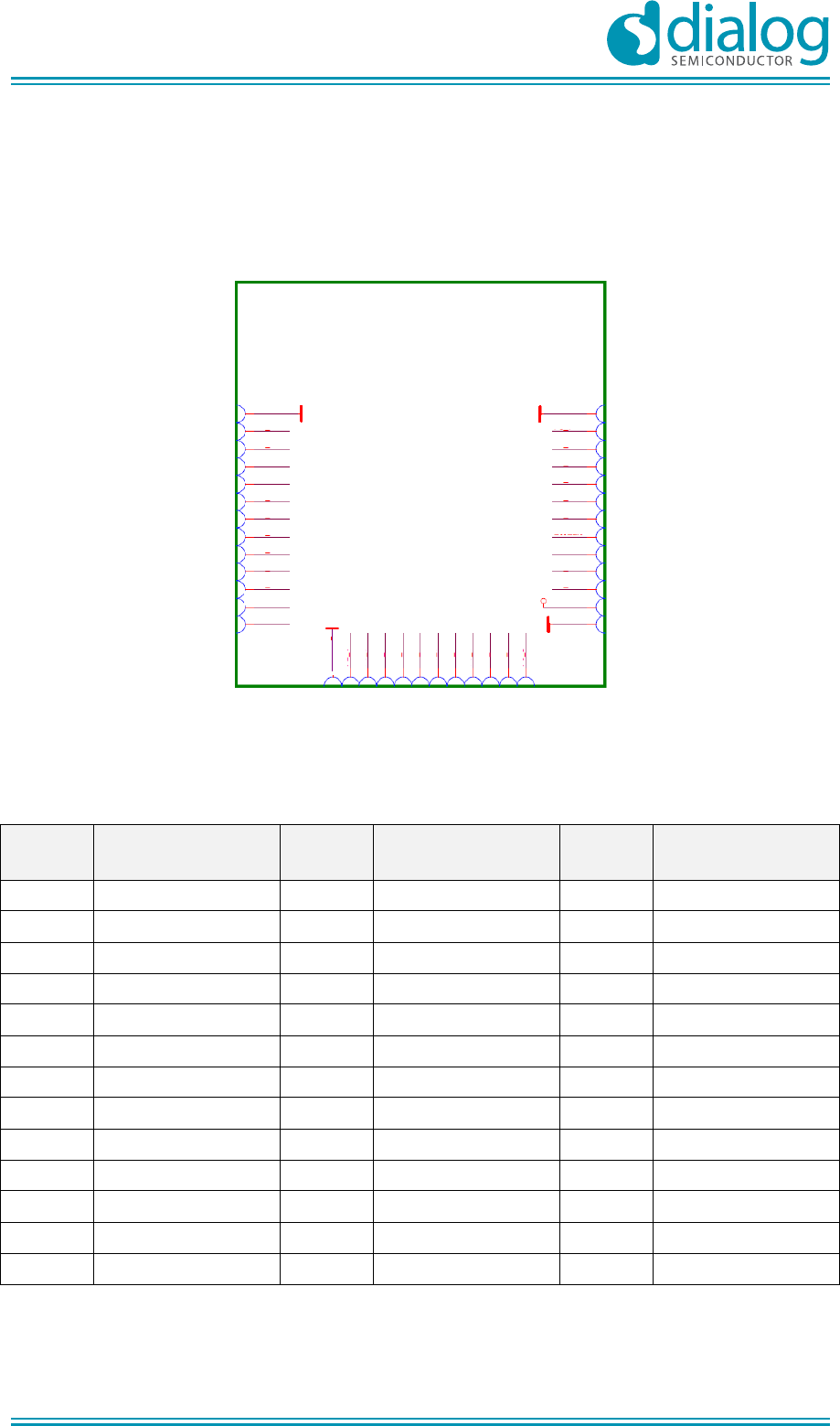
Module pinout
4.6
All available pins of the DA14580 SoC are routed out to the pins of the QFN48 antenna module.
Module pin numbers and names are given in Figure 3 and Table 2. The module pins use the
corresponding names of the DA14580 QFN48 integrated circuit.
1
2
3
4
5
6
7
8
9
10
11
12
13
14
15
16
17
18
19
20
21
22
23
24
25
38
37
36
35
34
33
32
31
30
29
28
27
26
Top View
P2_7
P2_8
VPP
P2_9
P2_0
P0_0
P0_1
P0_2
P0_3
P3_0
TXD/P0_4
RXD/P0_5
GND
P0_6
P3_1
P0_7
P3_2
P3_3
P2_2
P3_4
P2_3
P2_4
P3_5
P2_1
GND
P3_7
P2_6
P2_5
P3_6
P1_3
P1_2
SWCLK
SWDIO
P1_1
P1_0
GND
GND
Vbat
Figure 3: Module pin locations
Table 2: Module pin assignment (top view)
Pin no. Pin name
(PCB left side)
Pin no. Pin name
(PCB bottom side)
Pin no. Pin name
(PCB right side)
1 GND 14 GND 26 GND
2 P2_7 15 P2_1 27 VBAT
3 P2_8 16 P0_6 28 P1_0
4 VPP 17 P3_1 29 P1_1
5 P2_9 18 P0_7 30 SWDIO
6 P2_0 19 P3_2 31 SW_CLK
7 P0_0 20 P3_3 32 P1_2
8 P0_1 21 P2_2 33 P1_3
9 P0_2 22 P3_4 34 P3_6
10 P0_3 23 P2_3 35 P2_5
11 P3_0 24 P2_4 36 P2_6
12 P0_4 (TxD) 25 P3_5 37 P3_7
13 P0_5 (RxD) 38 GND
UM-B-036
DA14580 Antenna module for QFN48 package
User manual
Revision 2.0
10
-
Dec
-
2014
CFR0012-00 Rev 1 11 of 34 © 2014
Dialog Semiconductor
Module GPIOs
4.7
The QFN48 antenna module provides 32 general purpose input/output pins (including JTAG signals).
The interfaces are multiplexed with the GPIOs and can be enabled by appropriate programming. The
available GPIO functions are presented in Table 3.
The following digital interfaces are available externally to the module:
●
Two UARTs with hardware flow control up to 1 MBd
●
SPI interface
●
I
2
C bus at 100 kHz, 400 kHz
●
3-axis capable quadrature decoder
In addition, a 4-channel 10-bit ADC is also available externally to the module.
Table 3: GPIO pins: available functions
Interface Description Pins Comments
UART1 (UTX, URX) Bootable UART
P00, P01 57.6 kBd on booting
P02, P03 115.2 kBd on booting
P04,P05 57.6 kBd on booting.
This combination is selected for
the UART on this module.
P06, P07 9.6 kBd on booting
UART1 (RTS, CTS) Bootable UART P02, P03
P06, P07
UART1 or UART2 UART debug port Any port and any pin
combination
SPI
Bootable SPI P00, P03, P05, P06 Up to 8 MHz.
Non-bootable SPI Any port and any pin
combination
I2C Bootable I
2
C
P00, P01
100 kHz on booting for all
combinations
P02, P03
P04, P05
P06, P07
Non-bootable I
2
C Any port, any pin
ADC P00, P01, P02, P03 The voltage on these pins must be
lower than V
BAT
.
Test points Frequency calibration P05 16 MHz oscillator output. Can be
used for clock calibration.
Interrupts
Any port and any pin
combination
Keypad Any port , any pin column or row
Reset
4.7.1
The reset signal of the DA14580 (pin RST) is active high. On the QFN48 antenna module the RST
pin of the DA14580 is connected to GND via a resistor R8 (0 Ω). Consequently, the only way to
perform a hardware reset of the DA14580 on the antenna module is by switching off the power.
UM-B-036
DA14580 Antenna module for QFN48 package
User manual
Revision 2.0
10
-
Dec
-
2014
CFR0012-00 Rev 1 12 of 34 © 2014
Dialog Semiconductor
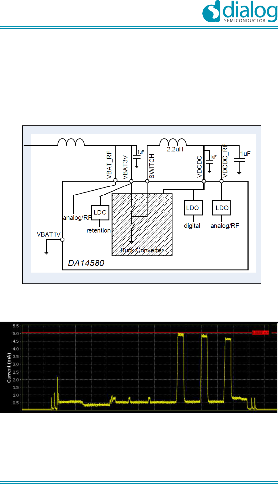
Power management
4.8
The QFN48 antenna module is supplied by a single power supply via pin 27 (VBAT). The supply
voltage of the module follows the specification of the DA14580 IC in buck configuration. The supply
voltage ranges from 2.4 V to 3.6 V.
Embedded in the DA14580, the DC/DC converter and LDOs produce all voltages required for the
system operation. The DC/DC converter is supplied from V
BAT
through a bead (FB1) and produces
1.4 V that feeds the internal LDOs. The LDOs supply the digital, analog and RF sections of the chip
with 1.2 V. Finally, the I/O ring is supplied from V
BAT
.
FB1
VBAT
C3
QFN48 Antenna module
Figure 4: Power management, DC/DC converter in buck configuration
The overall current consumption of the QFN48 antenna module in transmit mode is in the range of 5
mA, whereas in sleep mode the consumption is in the range of 2 µA. See Figure 5.
Figure 5: Current consumption during an Advertising frame
UM-B-036
DA14580 Antenna module for QFN48 package
User manual
Revision 2.0
10
-
Dec
-
2014
CFR0012-00 Rev 1 13 of 34 © 2014
Dialog Semiconductor
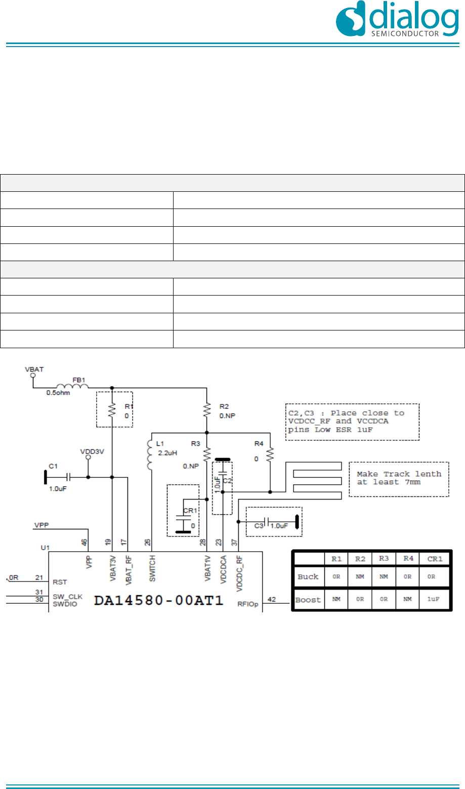
DC/DC converter in boost configuration
4.8.1
Supplying the QFN48 antenna module at a lower voltage (down to 0.9 V) is feasible, but modification
of the module’s components is needed. Please note that this configuration has not been used in the
tests for the FCC/ETSI certification.
Table 4: DA14580 DC/DC converter configurations
Buck configuration (default)
Supply voltage 2.4 V to 3.6 V
Populated components R1 = 0 Ω, R4 = 0 Ω, CR1 = 0 Ω
Not populated components R2, R3
FCC/CE certification Yes
Boost configuration
Supply voltage 0.9 V to 2.0 V (single cell alkaline battery)
Populated components R2 = 0 Ω, R3 = 0 Ω, CR1 = 1 µF
Not populated components R1, R4
FCC/CE certification No
Figure 6: DA14580 DC/DC converter circuit
Crystals
4.9
The frequency tolerance specification for BLE is ±50 ppm. To compensate for ageing and offset
effects, the external crystal of 16 MHz must have an accuracy of ±20 ppm or better. On the QFN48
antenna module the 16 MHz crystal (Y1) has a fundamental frequency of 16 MHz ±10 ppm and a
load capacitance of 10 pF. The crystal is located on the module itself. The crystal oscillator frequency
can be tuned using a programmable capacitance bank that is embedded in the DA14580.
For sleep mode the on-chip RCX oscillator is used (typ. 10 kHz). In addition, a 32.768 kHz crystal
(Y2) with a tolerance of ±50 ppm can be mounted on the module.
UM-B-036
DA14580 Antenna module for QFN48 package
User manual
Revision 2.0
10
-
Dec
-
2014
CFR0012-00 Rev 1 14 of 34 © 2014
Dialog Semiconductor
Table 5: Crystal characteristics
Frequency Accuracy Load capacitance Size Placement
16 MHz ±10 ppm 10 pF 2.5 mm x 2.0 mm Populated
32.768 kHz ±20 ppm 7 pF 3.2 mm x 1.5 mm Optional
Note: When the DC/DC converter configuration is changed to boost mode, a 32.768 kHz crystal
must be mounted. The on-chip RCX oscillator can only be used in buck mode.
OTP programming
4.10
For programming the OTP memory of the DA14580, a DC voltage of 6.7 V (typ.) must be applied to
pin 4 (VPP).
Debugging/testing ports
4.11
Two ports are available for testing/debugging or software development: JTAG and UART: The pin
assignments of these ports are given in Table 6.
Table 6: QFN48 antenna module debug ports
Function QFN48 antenna module DA14580
Pin name Pin no. Pin name Pin no.
UART transmit (UTX) TxD 13 P0_5 7
UART receive (URX) RxD 12 P0_4 6
JTAG data SWDIO 30 SWDIO 30
JTAG clock SWCLK 31 SWCLK 31
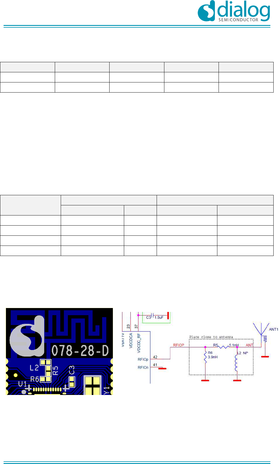
RF section
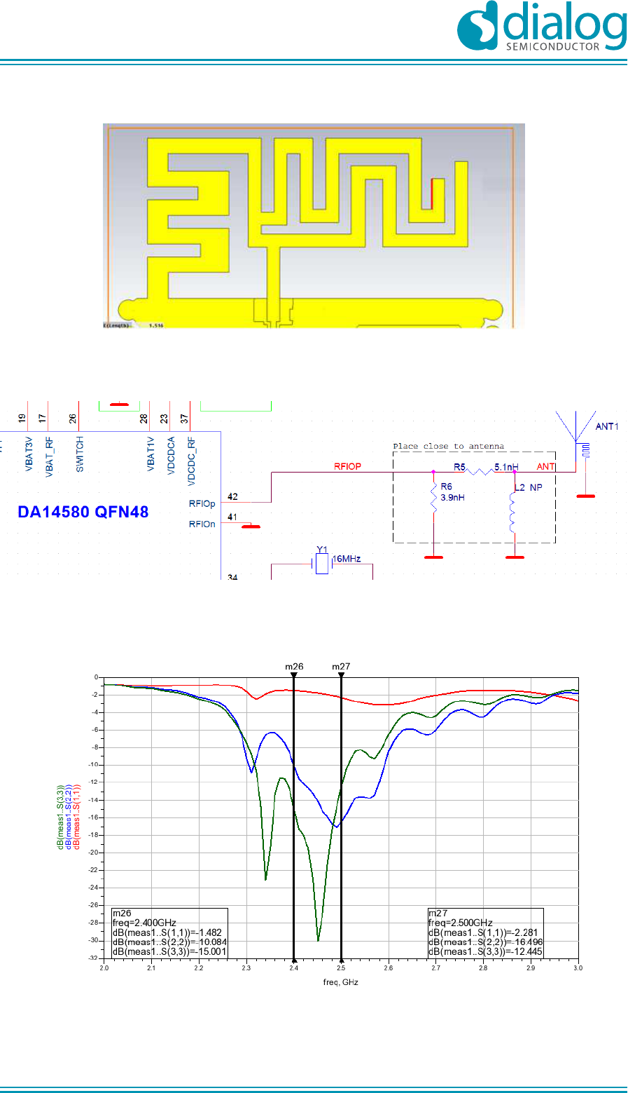
4.12
The DA14580 has a single pin RF input/output port. The RF section of the QFN48 antenna module
consists of a printed antenna and the matching network of R5, R6 and L2. L2 is not populated. See
Figure 7.
Figure 7: RF section: PCB layout (left) and schematic (right)
Antenna
4.12.1
A broadband variant of a printed F-antenna is used. A matching network is required for achieving the
maximum power transfer possible. The matching network consists of two inductances: R5 (series
coil: 5.1 nH, 0402, LQP series) and R6 (shunt coil: 3.9 nH, 0402, LQP series).
UM-B-036
DA14580 Antenna module for QFN48 package
User manual
Revision 2.0
10
-
Dec
-
2014
CFR0012-00 Rev 1 15 of 34 © 2014
Dialog Semiconductor
Figure 8: Antenna geometry
Figure 9: Matching network: R5 (5.1 nH) and R6 (3.9 nH)
Red: no matching
Blue: R5 = 4.7 nH, R6 = 3.9 nH
Green: R5 = 5.1 nH, R6 = 3.9 nH
UM-B-036
DA14580 Antenna module for QFN48 package
User manual
Revision 2.0
10
-
Dec
-
2014
CFR0012-00 Rev 1 16 of 34 © 2014
Dialog Semiconductor
Figure 10: Antenna VSWR measurements
4.12.1.1 Radiation diagrams
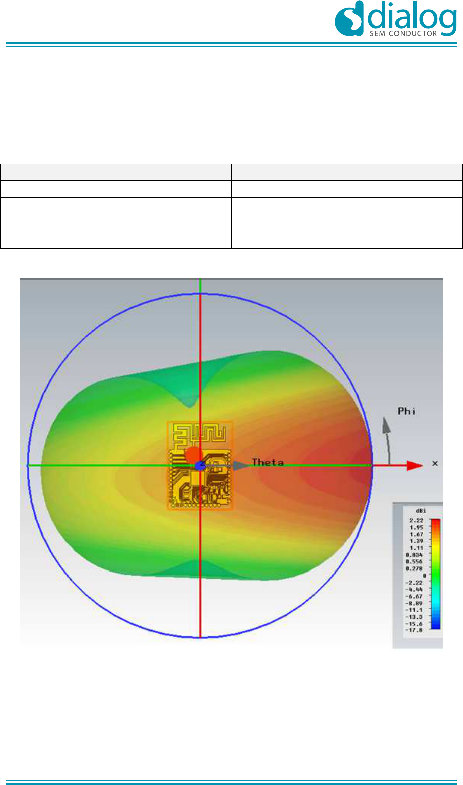
Gain calculations were performed. The maximum gain was measured at 2.225 dBi. See Table 7.
Table 7: Far field antenna parameters @ 2.44 GHz
Parameter Value
Frequency 2.44 GHz
Radiation efficiency -1.882 dB
Total efficiency -6.662 dB
Directivity 2.225 dBi
Figure 11: Far field antenna directivity @ 2.44 GHz
UM-B-036
DA14580 Antenna module for QFN48 package
User manual
Revision 2.0
10
-
Dec
-
2014
CFR0012-00 Rev 1 17 of 34 © 2014
Dialog Semiconductor
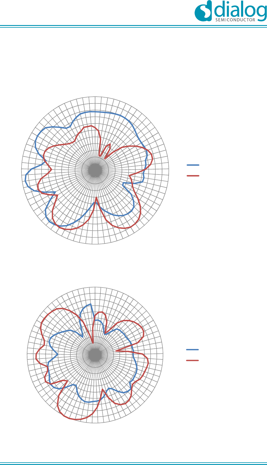
4.12.1.2 Radiation pattern measurements
Measurements of the radiation pattern in an anechoic chamber for vertical and horizontal positions of
the module are given in Figure 12 and Figure 13, respectively.
Figure 12: Radiation diagram for the module placed vertically on the long edge
Figure 13: Radiation diagram for the module placed horizontally
-30
-27
-24
-21
-18
-15
-12
-9
-6
-3
0
3
12345678910
11
12
13
14
15
16
17
18
19
20
21
22
23
24
25
26
27
28
29
30
31
32
33
34
35
36
3738
39
40
41
42
43
44
45
46
47
48
49
50
51
52
53
54
55
56
57
58
59
60
61
62
63
64
65
66
67686970717273
Vertical polarization
Horizontal polarization
-30
-27
-24
-21
-18
-15
-12
-9
-6
-3
0
3
12345678910
11
12
13
14
15
16
17
18
19
20
21
22
23
24
25
26
27
28
29
30
31
32
33
34
35
36
3738
39
40
41
42
43
44
45
46
47
48
49
50
51
52
53
54
55
56
57
58
59
60
61
62
63
64
65
66
67
686970717273
Vertical polarization
Horizontal polarization
UM-B-036
DA14580 Antenna module for QFN48 package
User manual
Revision 2.0
10
-
Dec
-
2014
CFR0012-00 Rev 1 18 of 34 © 2014
Dialog Semiconductor
Tuning the 16 MHz crystal
4.13
The accuracy of the 16 MHz crystal (±10ppm) guarantees the ‘in spec’ operation of the QFN48
antenna module. However, further trimming of the 16 MHz crystal is possible using the procedure
that is described in AN-B-020 End product testing and programming guidelines. See Ref.[2].
Software
4.14
The standard SDK release software, without modifications, can be used for testing or operating the
QFN48 antenna module.
Test platform
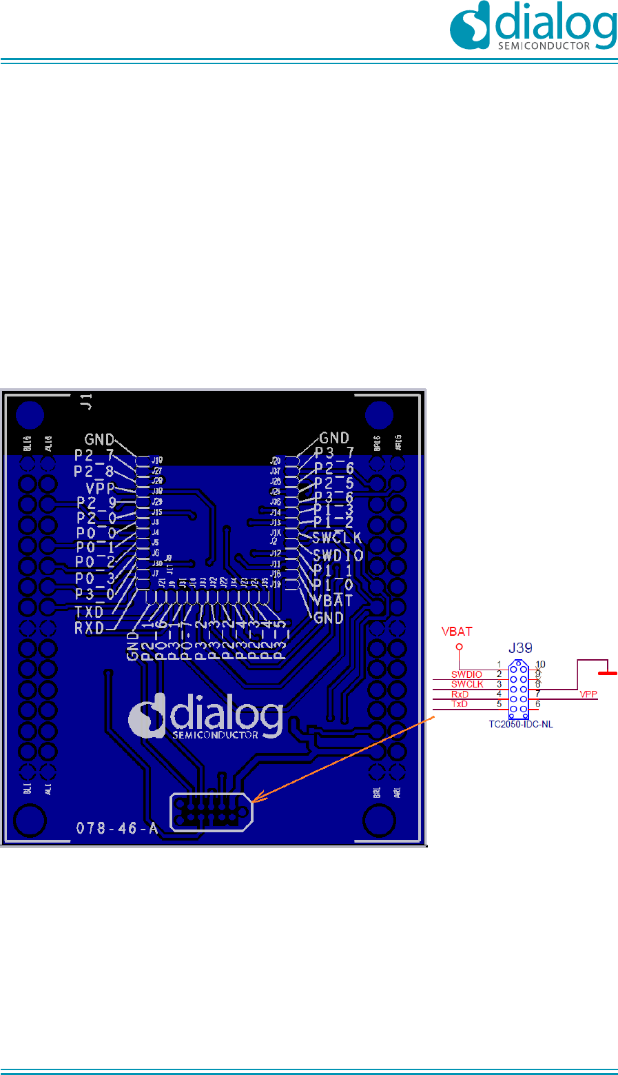
4.15
An interposer (078-46-A) was built for hardware interfacing the Expert DK Motherboard (580-MB-vC2
/ 078-10-C2) to the QFN48 antenna module. The interposer can be used as a stand-alone platform,
as it has a debug port (J39). The debug port consist of JTAG, UART, VPP, VBAT and GND signals.
Figure 14: Interposer (078-46-A) for the QFN48 antenna module
UM-B-036
DA14580 Antenna module for QFN48 package
User manual
Revision 2.0
10
-
Dec
-
2014
CFR0012-00 Rev 1 19 of 34 © 2014
Dialog Semiconductor
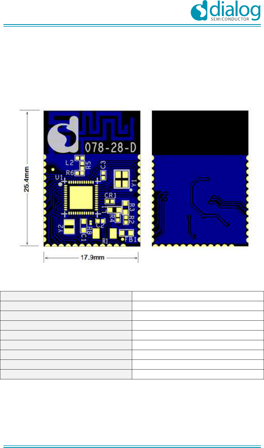
PCBA
4.16
A two-layer FR4 PCB with 1 mm standard thickness is used. The PCB size is 25.4 mm x 17.9 mm.
There are 38 connection pads which are made as castellation (1/2 open drill) with 1.27 mm pitch.
The PCB layout is shown in Figure 15 and the fabrication parameters are given in Table 8.
The schematic diagram and BOM of the QFN48 antenna module are presented in Figure 16 and
Table 9, respectively.
Figure 15: Top view (left) and bottom view (right) of PCBA
Table 8: PCB fabrication parameters
Number of layers 2
Core material FR4 IMP – 1.0 mm
Top copper thickness 0.018 mm
Bottom copper thickness 0.018 mm
Outer layer track width 0.100 mm
Hole density <1000 per dm
2
Outer layer isolation distance 0.125 mm
Hole diameter 0.45 mm
Outer layer annular ring 0.100 mm
UM-B-036
DA14580 Antenna module for QFN48 package
User manual
Revision 2.0
10
-
Dec
-
2014
CFR0012-00 Rev 1 20 of 34 © 2014
Dialog Semiconductor
Figure 16: Schematic of the DA14580 QFN48 antenna module
UM-B-036
DA14580 Antenna module for QFN48 package
User manual
Revision 2.0
10
-
Dec
-
2014
CFR0012-00 Rev 1 21 of 34 © 2014
Dialog Semiconductor
Table 9: Bill of Materials
No Qty Description Part Ref Value Part Number Package Manufacturer
1 1 CAP CERM
1.0uF 16V X7R
0603 C1 1.0 µF 0603YC105K AT2A 0603 AVX Corporation
2 2 CAP MLCC,
0204, 1UF, 6.3V,
20%, X5R C2 C3 1.0 µF GRM155R70
G105KA12D 0402 Murata
Electronics
3 2 RES 0.0 OHM
1/16W 5% 0402
SMD CR1 R4 0 Ω CRCW04020
000Z0ED 0402 Vishay/Dale
4 1 FILTER
CHI0.5ohm 0.4A
0603 FB1 BLM18AG102 SN1D 0603 Murata
Electronics
5 1 INDUCTOR
Power 2.2uH,
500mA, 400MHz L1 2.2 µH BRL1608T 2R2M 0603 Taiyo Yuden
6 1
RESISTOR,
THICK FILM, 0
OHM, 250mW,
5%
R1 0 Ω RC1206JR- 070RL 1206 YAGEO
7 1 INDUCTOR RF,
0402, 5.1NH,
±0.3NH, 0.26ohm R5 5.1 nH L-07C5N1 SV6T 0402 JOHANSON
TECHNOLOGY
8 1 RF INDUCTOR
0402 3.9NH,
±0.3NH 0.22ohm R6 3.9 nH L-07C3N9 SV6T 0402 Johanson
Technology Inc
9 1 RESISTOR,
0201, 0R0 R8 0 Ω CRCW02010
000Z0ED 0201 VISHAY
DRALORIC
10 1
DA14580
Bluetooth Low
Energy SOC –
QFN48
U1 DA14580-00AT1 QFN48, 6x
6 x 0.9mm DIALOG SEMI
11 1 CRYSTAL
16.000MHZ 10PF
SMT Y1 16 MHz 7M-16.000 MEEQ-T xtal4p
25x20 TXC
Not Populated
1 1 Inductor L2 NM
0402
2 1 Resistor R3 0 Ω
0603
3 1 crystal
32.768KHZ,
±20ppm, 7PF Y2 32.768
kHz ABS06-32.768KHz-
7-T 2x1.2mm Abracon
Corporation
4 1 Resistor R2 0 Ω CRCW0402 0000
Z0ED 0402 Vishay/Dale
UM-B-036
DA14580 Antenna module for QFN48 package
User manual
Revision 2.0
10
-
Dec
-
2014
CFR0012-00 Rev 1 22 of 34 © 2014
Dialog Semiconductor
5 Measurements
Receiver sensitivity (conducted)
5.1
Test description
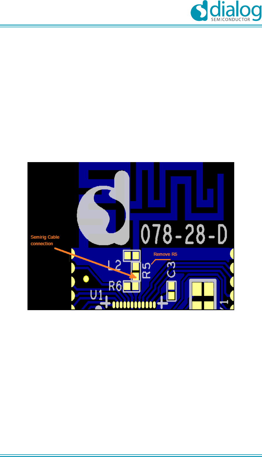
5.1.1
In this test the conducted RF sensitivity of the QFN48 antenna module was measured.
Test setup
5.1.2
The supply voltage (3.0 V DC) was connected between the PCB pads 27 (VBAT) and 26 (GND).
The R&S
®
CBT Bluetooth
®
Tester from Rohde & Schwarz was used. Component R5 was removed.
The semi-rigid cable was soldered at this pad. See Figure 17.
Figure 17: Test setup for the conducted RF measurements
Test results
5.1.3
The conducted RF sensitivity using a ‘dirty’ transmitter is better than -90 dBm for most channels.
Lower sensitivity has been noticed on some channels. This is caused by harmonics of the 16 MHz
oscillator. The results for one of the modules are shown Table 10.
UM-B-036
DA14580 Antenna module for QFN48 package
User manual
Revision 2.0
10
-
Dec
-
2014
CFR0012-00 Rev 1 23 of 34 © 2014
Dialog Semiconductor
Table 10: Conducted receiver sensitivity
UM-B-036
DA14580 Antenna module for QFN48 package
User manual
Revision 2.0
10
-
Dec
-
2014
CFR0012-00 Rev 1 24 of 34 © 2014
Dialog Semiconductor
Transmitter output power (conducted)
5.2
Test description
5.2.1
In this test the conducted RF output power of the QFN48 antenna module was measured.
Test setup
5.2.2
The supply voltage (3.0 V DC) was connected between the PCB pads 27 (VBAT
)
and 26 (GND).
The integrated antenna was bypassed by removing component R5. A short RF semi-rigid cable was
connected to this pad. See Figure 17.
The R&S®CBT Bluetooth® Tester from Rohde & Schwarz was used. Bursts of 10 packets were
transmitted by the DA14580. The packet length was 37 bytes and the pattern was ‘01010101’.
Test results
5.2.3
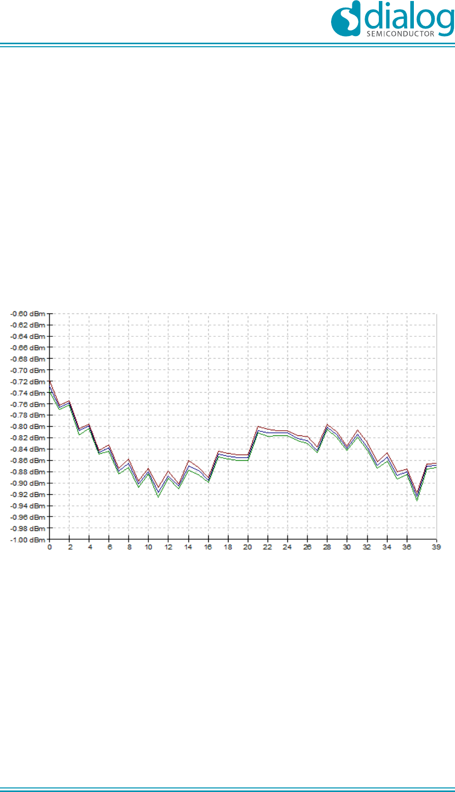
The results of the output power measurements for one of the modules are given in Figure 18.
Red: maximum
Blue: average
Green: minimum
Figure 18: Conducted output power per channel
Current consumption
5.3
Test setup
5.3.1
The board used in the test presented has optimal RF performance. The following instruments were
used for the test:
●
Multimeter
●
3 V, 100 mA power source for peak current
●
3 V, 10 µA power source for sleep current
UM-B-036
DA14580 Antenna module for QFN48 package
User manual
Revision 2.0
10
-
Dec
-
2014
CFR0012-00 Rev 1 25 of 34 © 2014
Dialog Semiconductor
●
Agilent N6705B DC Power Analyzer
Power consumption was measured using beacon firmware. During this test the transmit peak current
(in Advertising mode) and the sleep current were measured.
Test results
5.3.2
For this measurement the DUT was supplied by 3 V. Firmware was downloaded and the JTAG
programmer was disconnected. The firmware was controlling the RF switches.
Table 11: Peak current during Advertising mode
Parameter Value
I
BAT_TX
4.62 mA
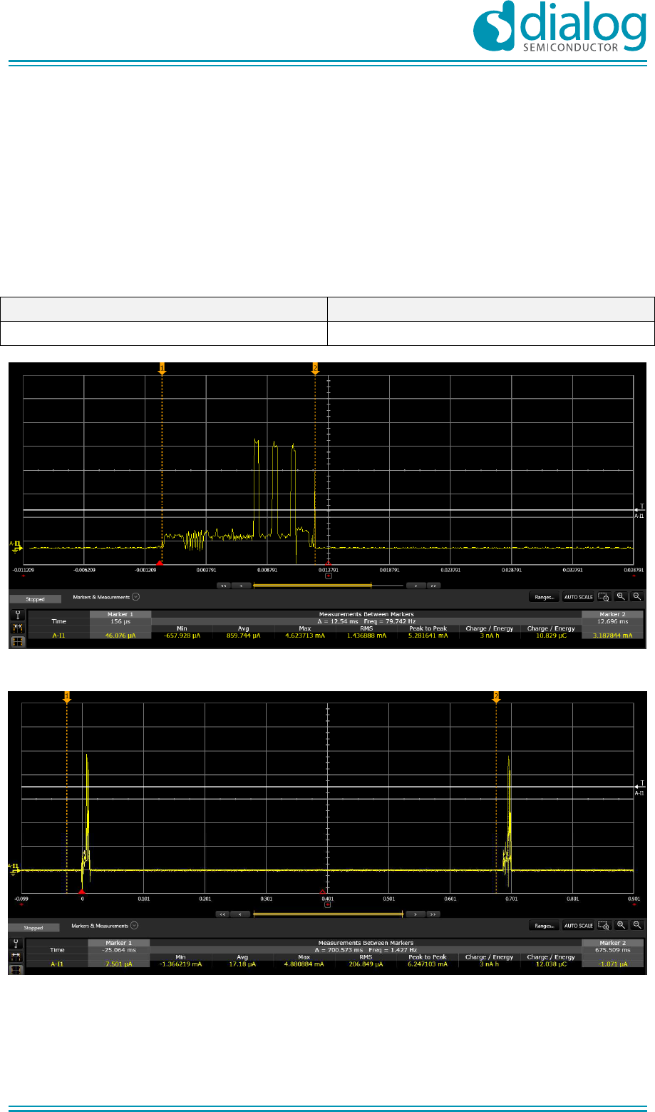
Figure 19: Supply current during an Advertising frame
Figure 20: Supply current during periodic transmissions every 700 ms
UM-B-036
DA14580 Antenna module for QFN48 package
User manual
Revision 2.0
10
-
Dec
-
2014
CFR0012-00 Rev 1 26 of 34 © 2014
Dialog Semiconductor
Table 12: Average current in Extended Sleep mode
Parameter Value
I
BAT_SLP
~ 2 µA
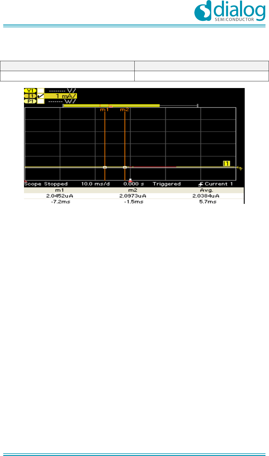
Figure 21: Supply current during Extended Sleep mode

UM-B-036
DA14580 Antenna module for QFN48 package
User manual
Revision 2.0
10
-
Dec
-
2014
CFR0012-00 Rev 1 27 of 34 © 2014
Dialog Semiconductor
6 FCC/IC Certification and CE marking
Standards and conformity assessment
6.1
The QFN48 antenna module was tested and found compliant by a qualified laboratory to the
following standards:
For FCC/IC certification:
●
Complete RF testing according to FCC part 15.247, 15.209.
●
FCC Rules and Regulations 47 CFR Chapter I Part 15 Subpart B (10-01-12 Edition) and ICES-
003 ISSUE 5. This covers:
o Continuous Conducted Emission of Power Leads, frequency range 0.15 ÷ 30 MHz.
o Radiated Emission – Electromagnetic field, frequency range 30 MHz ÷ 26 GHz
For CE marking:
●
Complete RF testing according to ETSI EN 300 328 v1.8.1
●
EMC testing according to EN 301 489-1 V.1.9.2 & EN 301 489-17 V2.2.1
o Radiated Emission- Electromagnetic Field measure. Frequency Range 30 MHz ÷ 6 GHz.
Test standard EN 55022 (2010)/ AC(2011).
o Radiated RF Electromagnetic Field Immunity Test. Frequency Range 80 MHz ÷ 2.7 GHz.
Test standard, EN 61000-4-3 (2006) / A1 (2008) / A2 (2010).
●
Electrical Safety testing according to EN 61010-1: 2010
o Electrostatic Discharge Immunity Test. Test standard EN 61000-4-2
●
RoHS 2011/65/CE (includes screening for 20 elements).

UM-B-036
DA14580 Antenna module for QFN48 package
User manual
Revision 2.0
10
-
Dec
-
2014
CFR0012-00 Rev 1 28 of 34 © 2014
Dialog Semiconductor
FCC requirements regarding the end product and end user
6.2
End product marking
6.2.1
The end product that the module is integrated into must be marked as follows:
“Contains Transmitter Module FCC ID: Y82DA14580REFANT / IC: 9567A-DA14580REFANT”
“Module transmetteur ID IC: 9567A-DA14580REFANT”
End product literature
6.2.2
The literature that is provided to the end user must include the following wording:
“Dialog Semiconductor does not approve any changes or modifications made to this device by the
user. Any changes or modifications could void the user’s authority to operate the equipment.
Dialog Semiconductor n’approuve aucune modification apportée à l’appareil par l’utilisateur, quelle
qu’en soit la nature. Tout changement ou modification peuvent annuler le droit d’utilisation de
l’appareil par l’utilisateur.
This device complies with Part 15 of the FCC Rules and Industry Canada licence-exempt RSS
standard(s). Operation is subject to the following two conditions: (1) this device may not cause
interference, and (2) this device must accept any interference, including interference that may cause
undesired operation of the device.
Le présent appareil est conforme aux CNR d'Industrie Canada applicables aux appareils radio
exempts de licence. L'exploitation est autorisée aux deux conditions suivantes : (1) l'appareil ne doit
pas produire de brouillage, et (2) l'utilisateur de l'appareil doit accepter tout brouillage radioélectrique
subi, même si le brouillage est susceptible d'en compromettre le fonctionnement.
This device complies with FCC/IC radiation exposure limits set forth for an uncontrolled environment
and meets the FCC radio frequency (RF) Exposure Guidelines and RSS‐102 of the IC radio
frequency (RF) Exposure rules. This transmitter must not be co-located or operating in conjunction
with any other antenna or transmitter.
Le présent appareil est conforme à l'exposition aux radiations FCC / IC définies pour un
environnement non contrôlé et répond aux directives d'exposition de la fréquence de la FCC
radiofréquence (RF) et RSS
‐
102 de la fréquence radio (RF) IC règles d'exposition. L'émetteur ne doit
pas être colocalisé ni fonctionner conjointement avec à autre antenne ou autre émetteur.
This equipment has been tested and found to comply with the limits for a Class B digital device,
pursuant to part 15 of the FCC Rules. These limits are designed to provide reasonable protection
against harmful interference in a residential installation.
This equipment generates, uses and can radiate radio frequency energy and, if not installed and
used in accordance with the instructions, may cause harmful interference to radio communications.
However, there is no guarantee that interference will not occur in a particular installation.
If this equipment does cause harmful interference to radio or television reception, which can be
determined by turning the equipment off and on, the user is encouraged to try to correct the
interference by one or more of the following measures:
●
Reorient or relocate the receiving antenna.
●
Increase the separation between the equipment and receiver.
●
Connect the equipment into an outlet on a circuit different from that to which the receiver is
connected.
●
Consult the dealer or an experienced radio/TV technician for help.”

UM-B-036
DA14580 Antenna module for QFN48 package
User manual
Revision 2.0
10
-
Dec
-
2014
CFR0012-00 Rev 1 29 of 34 © 2014
Dialog Semiconductor
Industry Canada requirements regarding the end product and end user
6.3
End product marking
6.3.1
The host device shall be properly labelled to identify the modules within the host device. The Industry
Canada certification label of a module shall be clearly visible at all times when installed in the host
device, otherwise the host device must be labelled to display the Industry Canada certification
number of the module, preceded by the words "Contains transmitter module", or the word "Contains",
or similar wording expressing the same meaning, as follows:
“Contains transmitter module IC: 9567A-DA14580REFANT”
L'appareil hôte doit être étiqueté comme il faut pour permettre l'identification des modules qui s'y
trouvent. L'étiquette de certification d'Industrie Canada d'un module donné doit être posée sur
l'appareil hôte à un endroit bien en vue en tout temps. En l'absence d'étiquette,l'appareil hôte doit
porter une etiquette donnant le numéro de certification du module d'Industrie Canada, précédé des
mots "Contient un module d'émission", du mot "Contient" ou d'une formulation similaire exprimant le
même sens, comme suit:
“Contient le module d'émission IC: 9567A-DA14580REFANT”
End product literature
6.3.2
The literature that is provided to the end user must include the following wordings:
“This device complies with Industry Canada licence-exempt RSS standard(s). Operation is subject to
the following two conditions: (1) this device may not cause interference, and (2) this device must
accept any interference, including interference that may cause undesired operation of the device.
Le présent appareil est conforme aux CNR d'Industrie Canada applicables aux appareils radio
exempts de licence. L'exploitation est autorisée aux deux conditions suivantes : (1) l'appareil ne doit
pas produire de brouillage, et (2) l'utilisateur de l'appareil doit accepter tout brouillage radioélectrique
subi, même si le brouillage est susceptible d'en compromettre le fonctionnement.”
CAN ICES-3 (B) / NMB-3 (B)
“This Class B digital apparatus complies with Canadian ICES-003.
Cet appareil numérique de classe B est conforme à la norme canadienne ICES-003.”
1999/5/EC Directive
6.4
This device has been evaluated against the essential requirements of the 1999/5/EC Directive.
Bulgarian С настоящето Dialog Semiconductor BV декларира, че QFN48 BLUETOOTH
MODULE отговаря на съществените изисквания и другите приложими
изисквания на Директива 1999/5/ЕС.
Czech Dialog Semiconductor BV tímto prohlašuje, že tento QFN48 BLUETOOTH MODULE
je ve shodě se základními požadavky a dalšími příslušnými ustanoveními směrnice
1999/5/ES.
Danish Undertegnede Dialog Semiconductor BV erklærer herved, at følgende udstyr QFN48
BLUETOOTH MODULE overholder de væsentlige krav og øvrige relevante krav i
direktiv 1999/5/EF.
UM-B-036
DA14580 Antenna module for QFN48 package
User manual
Revision 2.0
10
-
Dec
-
2014
CFR0012-00 Rev 1 30 of 34 © 2014
Dialog Semiconductor
Dutch Hierbij verklaart Dialog Semiconductor BV dat het toestel QFN48 BLUETOOTH
MODULE in overeenstemming is met de essentiële eisen en de andere relevante
bepalingen van richtlijn 1999/5/EG.
English Hereby, Dialog Semiconductor BV, declares that this QFN48 BLUETOOTH MODULE
is in compliance with the essential requirements and other relevant provisions of
Directive 1999/5/EC.
Estonian Käesolevaga kinnitab Dialog Semiconductor BV seadme QFN48 BLUETOOTH
MODULE vastavust direktiivi 1999/5/EÜ põhinõuetele ja nimetatud direktiivist
tulenevatele teistele asjakohastele sätetele.
German Hiermit erklärt Dialog Semiconductor BV, dass sich das Gerät QFN48 BLUETOOTH
MODULE in Übereinstimmung mit den grundlegenden Anforderungen und den
übrigen einschlägigen Bestimmungen der Richtlinie 1999/5/EG befindet.
Greek ΜΕ ΤΗΝ ΠΑΡΟΥΣΑ Dialog Semiconductor BV ∆ΗΛΩΝΕΙ ΟΤΙ QFN48 BLUETOOTH
MODULE ΣΥΜΜΟΡΦΩΝΕΤΑΙ ΠΡΟΣ ΤΙΣ ΟΥΣΙΩ∆ΕΙΣ ΑΠΑΙΤΗΣΕΙΣ ΚΑΙ ΤΙΣ ΛΟΙΠΕΣ
ΣΧΕΤΙΚΕΣ ∆ΙΑΤΑΞΕΙΣ ΤΗΣ Ο∆ΗΓΙΑΣ 1999/5/ΕΚ.
Hungarian Alulírott, Dialog Semiconductor BV nyilatkozom, hogy a QFN48 BLUETOOTH
MODULE megfelel a vonatkozó alapvetõ követelményeknek és az 1999/5/EC irányelv
egyéb elõírásainak.
Finnish Dialog Semiconductor BV vakuuttaa täten että QFN48 BLUETOOTH MODULE
tyyppinen laite on direktiivin 1999/5/EY oleellisten vaatimusten ja sitä koskevien
direktiivin muiden ehtojen mukainen.
French Par la présente Dialog Semiconductor BV déclare que l'appareil QFN48 BLUETOOTH
MODULE est conforme aux exigences essentielles et aux autres dispositions
pertinentes de la directive 1999/5/CE.
Icelandic Hér með lýsir Dialog Semiconductor BV yfir því að QFN48 BLUETOOTH MODULE er
í samræmi við grunnkröfur og aðrar kröfur, sem gerðar eru í tilskipun 1999/5/EC
Italian Con la presente Dialog Semiconductor BV dichiara che questo QFN48 BLUETOOTH
MODULE è conforme ai requisiti essenziali ed alle altre disposizioni pertinenti stabilite
dalla direttiva 1999/5/CE.
Latvian Ar šo Dialog Semiconductor BV deklarē, ka QFN48 BLUETOOTH MODULE atbilst
Direktīvas 1999/5/EK būtiskajām prasībām un citiem ar to saistītajiem noteikumiem.
Lithuanian Šiuo Dialog Semiconductor BV deklaruoja, kad šis QFN48 BLUETOOTH MODULE
atitinka esminius reikalavimus ir kitas 1999/5/EB Direktyvos nuostatas.
Maltese Hawnhekk, Dialog Semiconductor BV, jiddikjara li dan QFN48 BLUETOOTH
MODULE jikkonforma mal-ħtiġijiet essenzjali u ma provvedimenti oħrajn relevanti li
hemm fid-Dirrettiva 1999/5/EC.
Norwegian Dialog Semiconductor BV erklærer herved at utstyret QFN48 BLUETOOTH MODULE
er i samsvar med de grunnleggende krav og øvrige relevante krav i direktiv
1999/5/EF.
UM-B-036
DA14580 Antenna module for QFN48 package
User manual
Revision 2.0
10
-
Dec
-
2014
CFR0012-00 Rev 1 31 of 34 © 2014
Dialog Semiconductor
Polish Niniejszym Dialog Semiconductor BV oświadcza, że QFN48 BLUETOOTH MODULE
jest zgodny z zasadniczymi wymogami oraz pozostałymi stosownymi
postanowieniami Dyrektywy 1999/5/EC
Portuguese Dialog Semiconductor BV declara que este QFN48 BLUETOOTH MODULE está
conforme com os requisitos essenciais e outras disposições da Directiva 1999/5/CE.
Slovak Dialog Semiconductor BV týmto vyhlasuje, že QFN48 BLUETOOTH MODULE spĺňa
základné požiadavky a všetky príslušné ustanovenia Smernice 1999/5/ES.
Slovenian Dialog Semiconductor BV izjavlja, da je ta QFN48 BLUETOOTH MODULE v skladu z
bistvenimi zahtevami in ostalimi relevantnimi določili direktive 1999/5/ES.
Spanish Por medio de la presente Dialog Semiconductor BV declara que QFN48
BLUETOOTH MODULE cumple con los requisitos esenciales y cualesquiera otras
disposiciones aplicables o exigibles de la Directiva 1999/5/CE.
Swedish Härmed intygar Dialog Semiconductor BV att denna QFN48 BLUETOOTH MODULE
står I överensstämmelse med de väsentliga egenskapskrav och övriga relevanta
bestämmelser som framgår av direktiv 1999/5/EG.
In order to satisfy the essential requirements of 1999/5/EC Directive, the product is compliant with
the following standards:
RF spectrum use (R&TTE art. 3.2) EN 300 328 v1.8.1
EMC (R&TTE art. 3.1b) EN 301 489-1 V1.9.2
EN 301 489-17 V2.2.1
Health & Safety (R&TTE art. 3.1a) EN 60950-1:2006 + A11:2009 + A1:2010 + A12:2011 +
AC:2011
EN 62479:2010
The conformity assessment procedure referred to in Article 10 and detailed in Annex IV of Directive
1999/5/EC has been followed with the involvement of the following Notified Body Notified Body:
AT4 wireless, S.A.
Parque Tecnologico de Andalucía
C/ Severo Ochoa 2
29590 Campanillas – Málaga
SPAIN
Notified Body No: 1909
Thus, the following marking is included in the product:

UM-B-036
DA14580 Antenna module for QFN48 package
User manual
Revision 2.0
10
-
Dec
-
2014
CFR0012-00 Rev 1 32 of 34 © 2014
Dialog Semiconductor
Full declaration of conformity can be found can be found on the customer portal
https://support.diasemi.com/
There is no restriction for the commercialisation of this device in all the countries of the European
Union.
RoHS compliance
6.4.1
Dialog Semiconductor complies to European Directive 2001/95/EC and from 2 January 2013
onwards to European Directive 2011/65/EU concerning Restriction of Hazardous Substances
(RoHS/RoHS2). Dialog Semiconductor’s statement on RoHS can be found on the customer portal
https://support.diasemi.com/. RoHS certificates from our suppliers are available on request.
1909

UM-B-036
DA14580 Antenna module for QFN48 package
User manual
Revision 2.0
10
-
Dec
-
2014
CFR0012-00 Rev 1 33 of 34 © 2014
Dialog Semiconductor
7 Revision history
Revision Date Description
1.0 21-Oct-2014 Initial version.
2.0 10-Dec-2014 1999/5/EC Directive added

UM-B-036
DA14580 Antenna module for QFN48 package
User manual
Revision 2.0
10
-
Dec
-
2014
CFR0012-00 Rev 1 34 of 34 © 2014
Dialog Semiconductor
Status definitions
Status Definition
DRAFT The content of this document is under review and subject to formal approval, which may result in
modifications or additions.
APPROVED
or unmarked
The content of this document has been approved for publication.
Disclaimer
Information in this document is believed to be accurate and reliable. However, Dialog Semiconductor does not give any
representations or warranties, expressed or implied, as to the accuracy or completeness of such information. Dialog
Semiconductor furthermore takes no responsibility whatsoever for the content in this document if provided by any information
source outside of Dialog Semiconductor.
Dialog Semiconductor reserves the right to change without notice the information published in this document, including without
limitation the specification and the design of the related semiconductor products, software and applications.
Applications, software, and semiconductor products described in this document are for illustrative purposes only. Dialog
Semiconductor makes no representation or warranty that such applications, software and semiconductor products will be
suitable for the specified use without further testing or modification. Unless otherwise agreed in writing, such testing or
modification is the sole responsibility of the customer and Dialog Semiconductor excludes all liability in this respect.
Customer notes that nothing in this document may be construed as a license for customer to use the Dialog Semiconductor
products, software and applications referred to in this document. Such license must be separately sought by customer with
Dialog Semiconductor.
All use of Dialog Semiconductor products, software and applications referred to in this document are subject to Dialog
Semiconductor’s Standard Terms and Conditions of Sale, unless otherwise stated.
© Dialog Semiconductor. All rights reserved.
RoHS Compliance
Dialog Semiconductor complies to European Directive 2001/95/EC and from 2 January 2013 onwards to European Directive
2011/65/EU concerning Restriction of Hazardous Substances (RoHS/RoHS2).
Dialog Semiconductor’s statement on RoHS can be found on the customer portal https://support.diasemi.com/. RoHS
certificates from our suppliers are available on request.
Contacting Dialog Semiconductor
United Kingdom (Headquarters)
Dialog Semiconductor PLC
Phone: +44 1793 757700
Germany
Dialog Semiconductor GmbH
Phone: +49 7021 805-0
The Netherlands
Dialog Semiconductor B.V.
Phone: +31 73 640 8822
North America
Dialog Semiconductor Inc.
Phone: +1 408 845 8500
Japan
Dialog Semiconductor K. K.
Phone: +81 3 5425 4567
Taiwan
Dialog Semiconductor Taiwan
Phone: +886 281 786 222
Singapore
Dialog Semiconductor Singapore
Phone: +65 64 849929
China
Dialog Semiconductor China
Phone: +86 21 5178 2561
Korea
Dialog Semiconductor Korea
Phone: +82 2 3469 8291
Email:
enquiry@diasemi.com
Web site:
www.dialog
-semiconductor.com