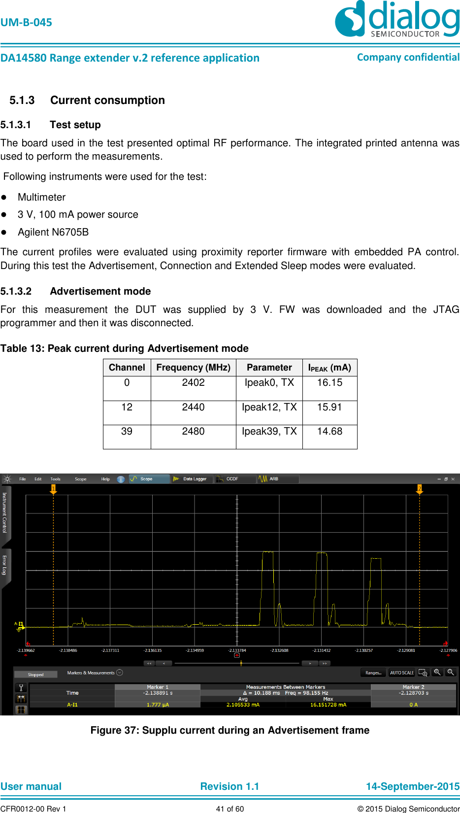
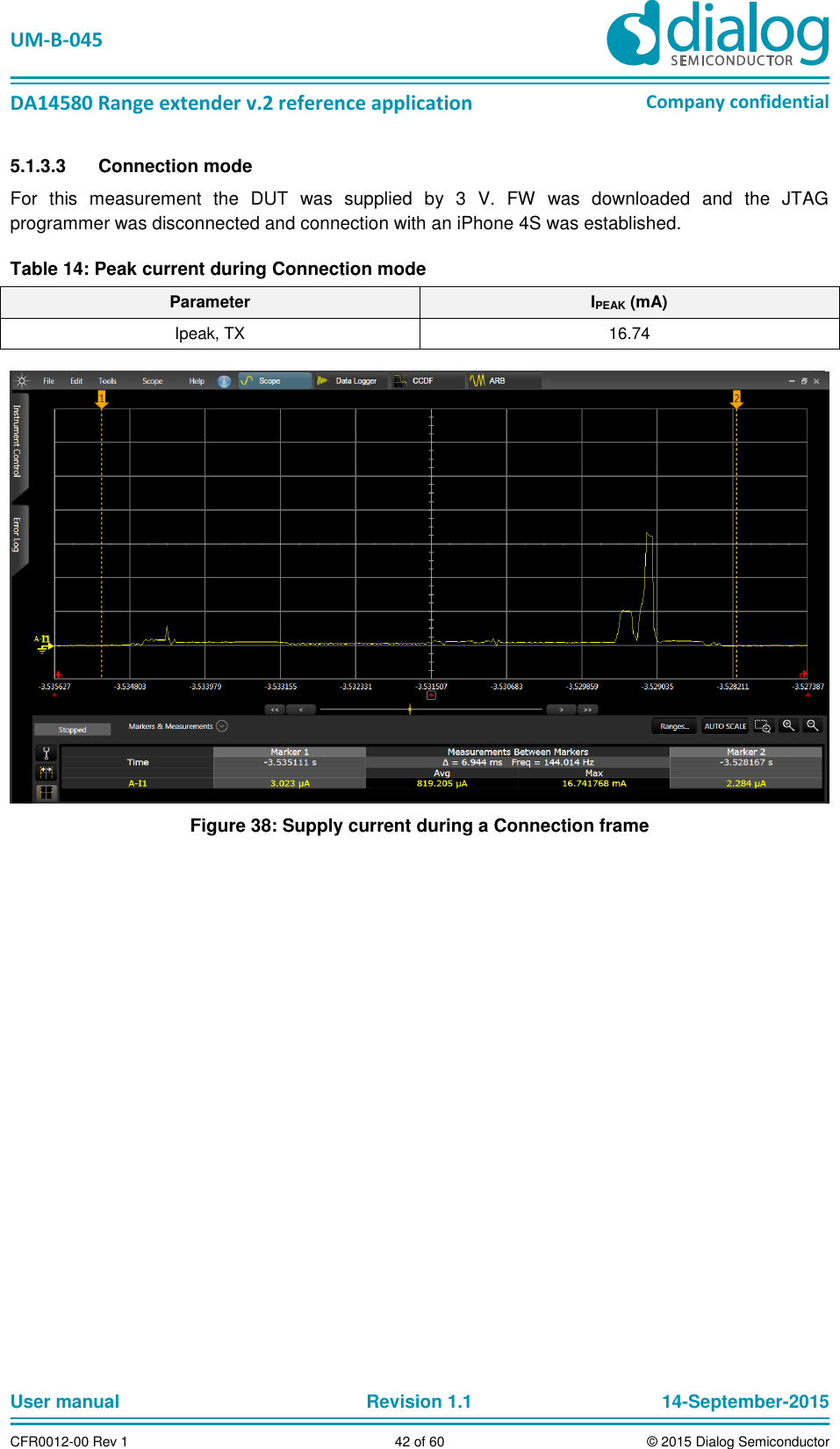
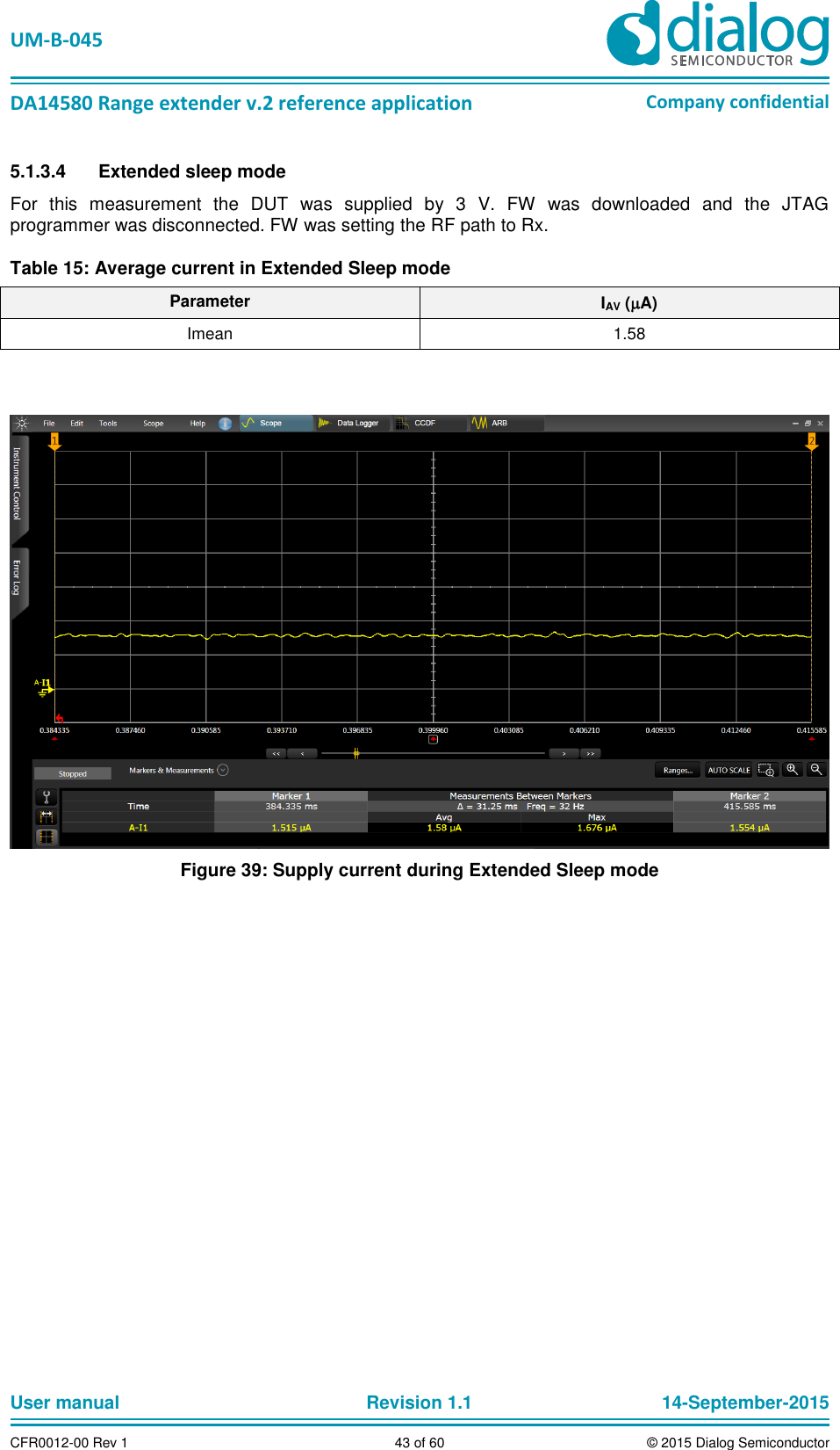
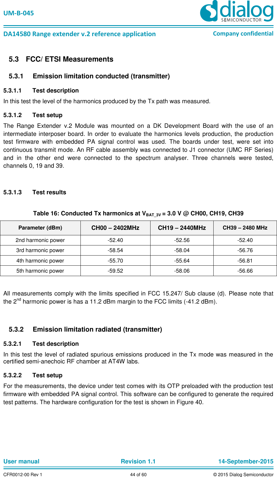
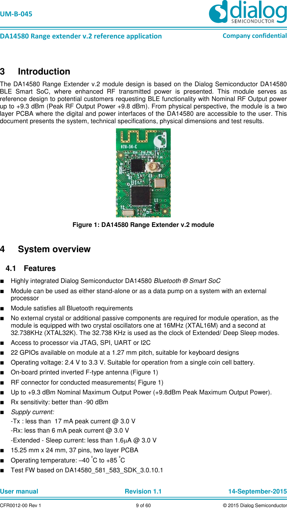
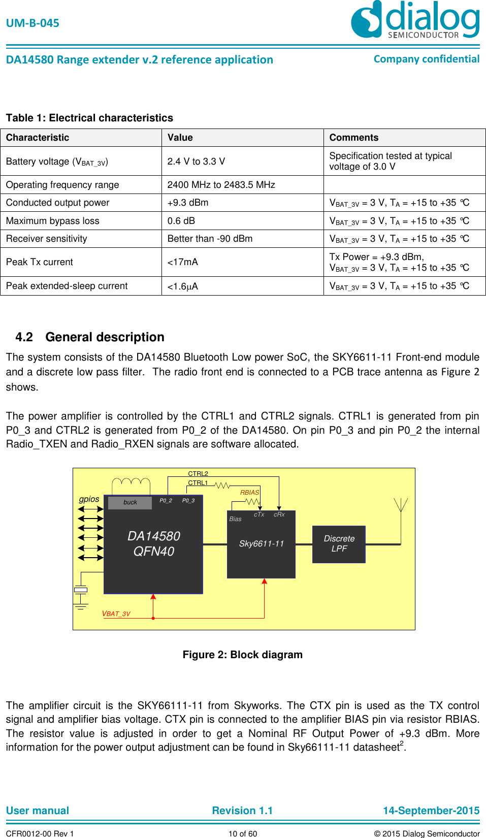
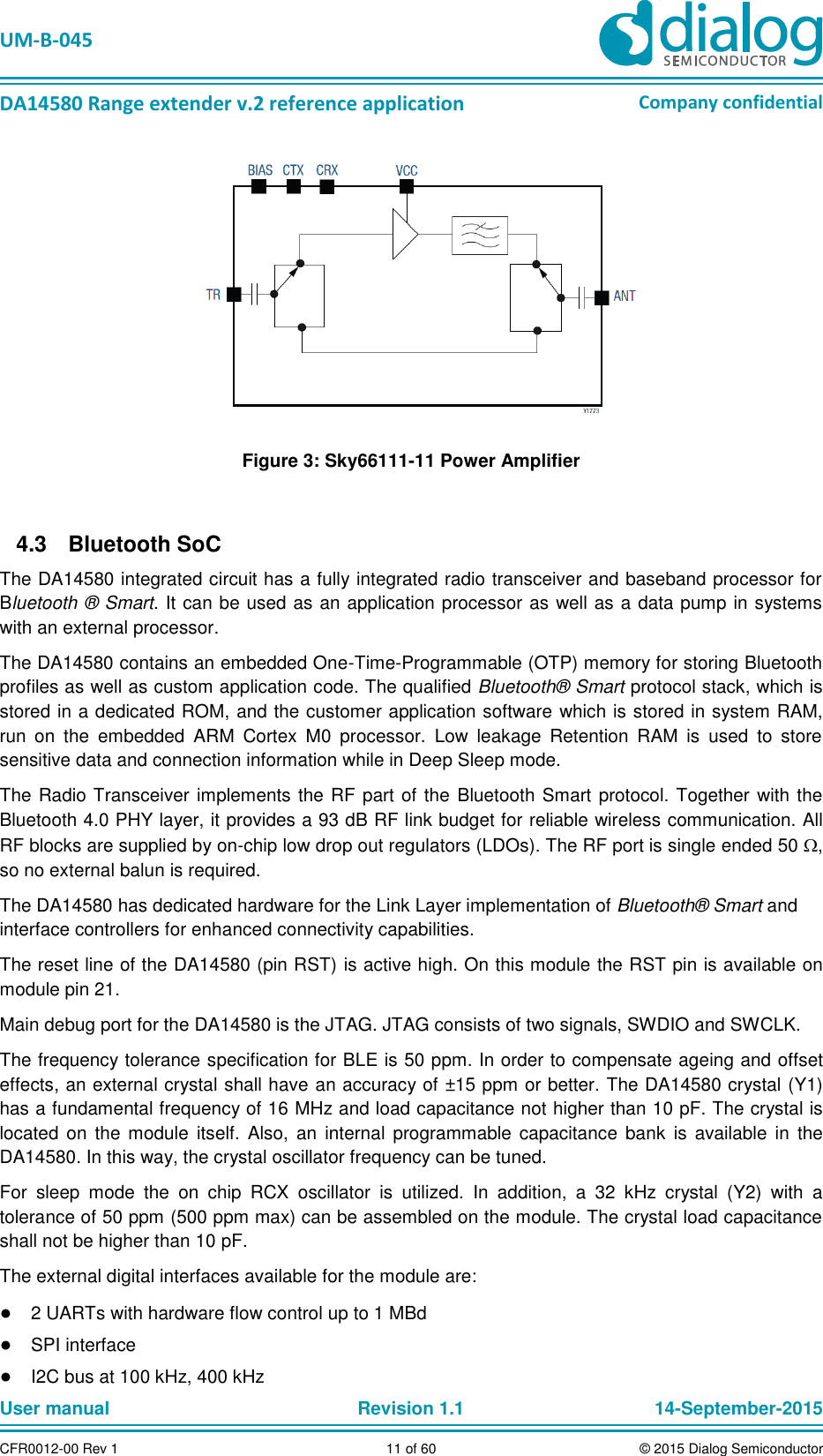
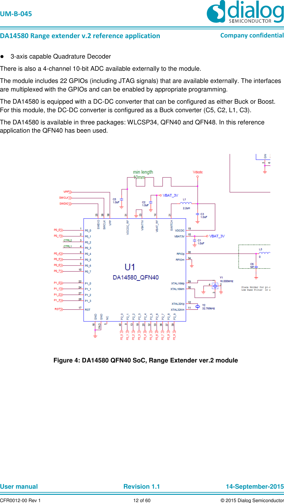
Dialog Semiconductor DA14580REXT BLE RF Module User Manual DA14580 Range extender v 2 reference application
Dialog Semiconductor BV BLE RF Module DA14580 Range extender v 2 reference application
UserManual.wiki
>
Dialog Semiconductor
>
DA14580REXT User Manual
User Manual
Navigation menu
Upload a User Manual
Namespaces
Wiki Guide
HTML
PDF
Info
Views
User Manual
Discussion / Help
Navigation
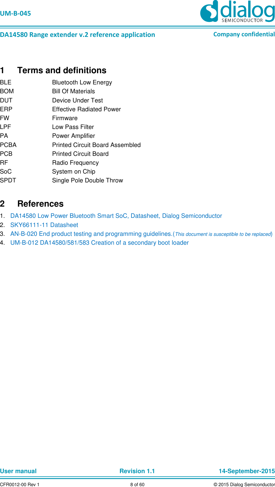
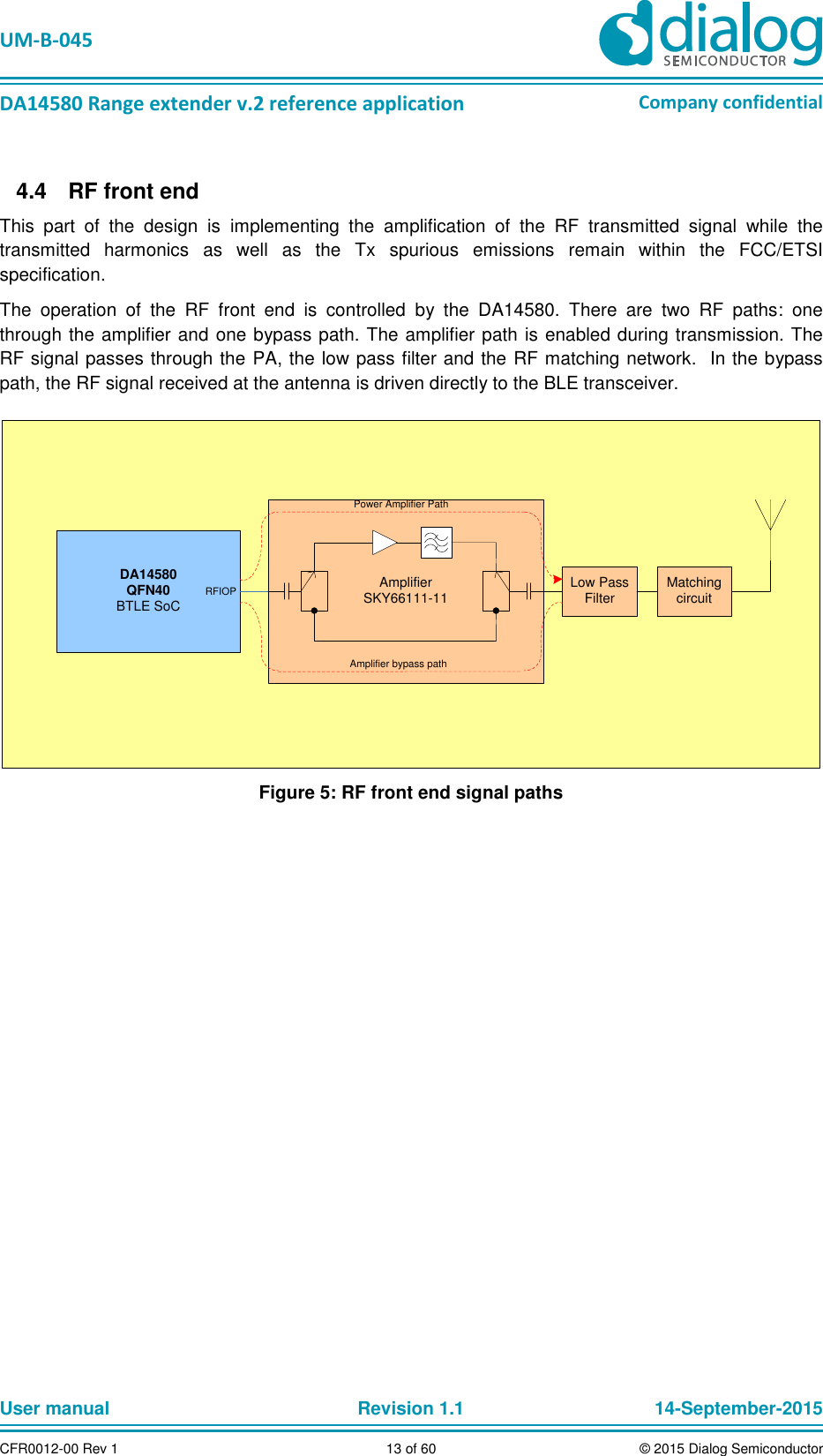
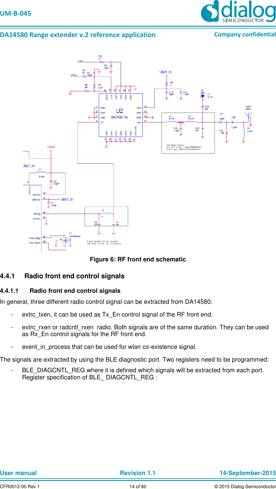
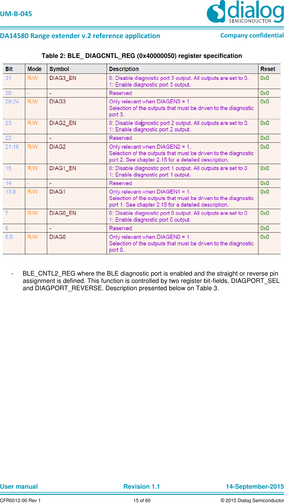
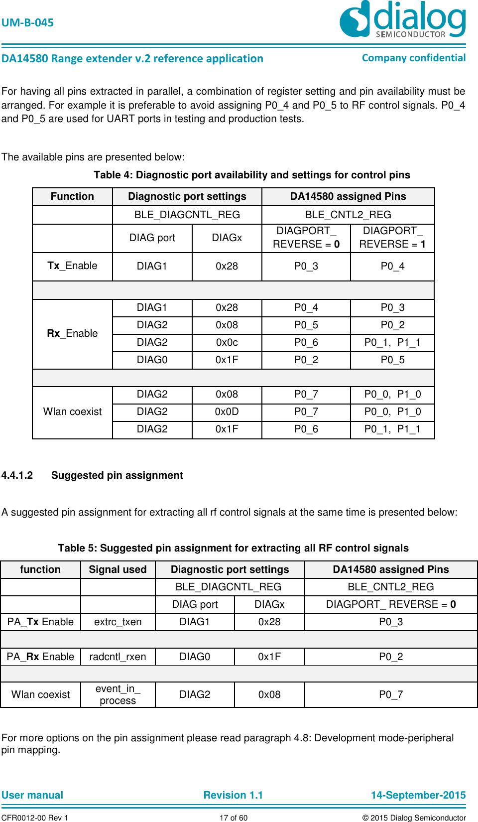
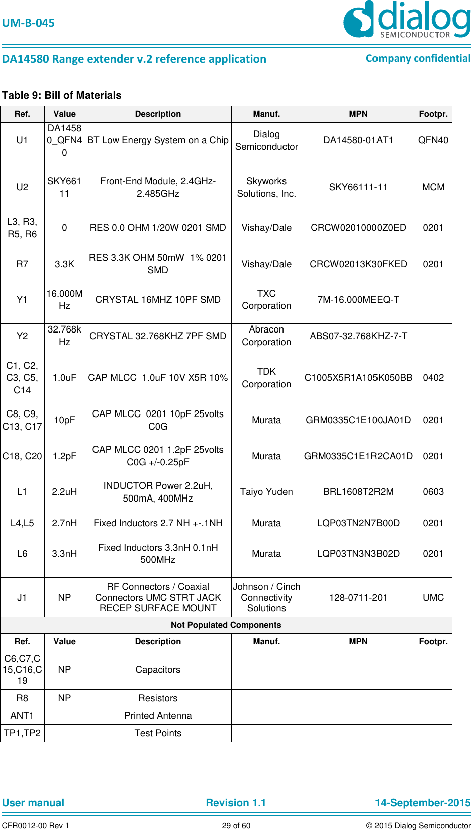
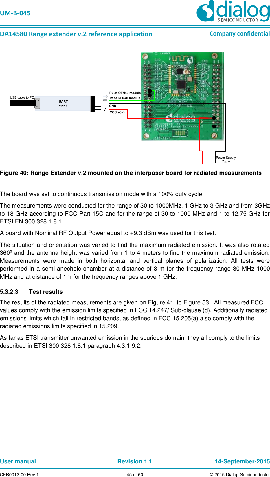
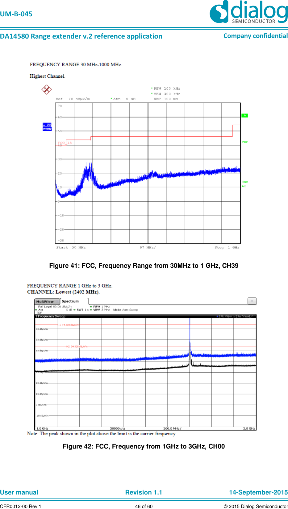
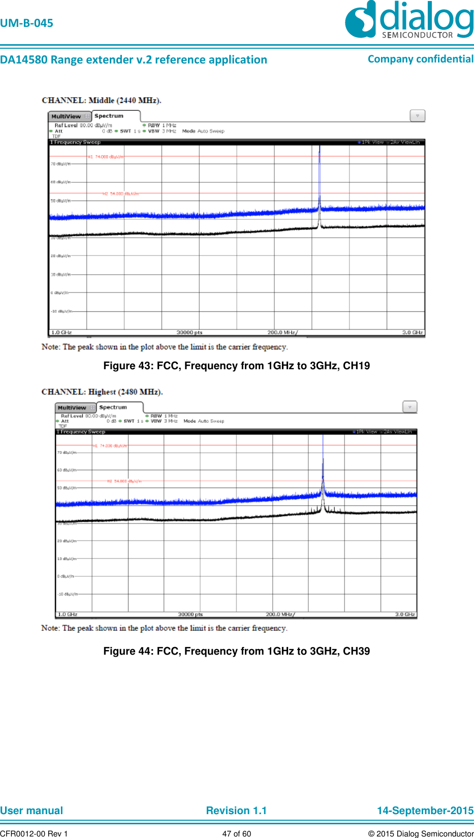
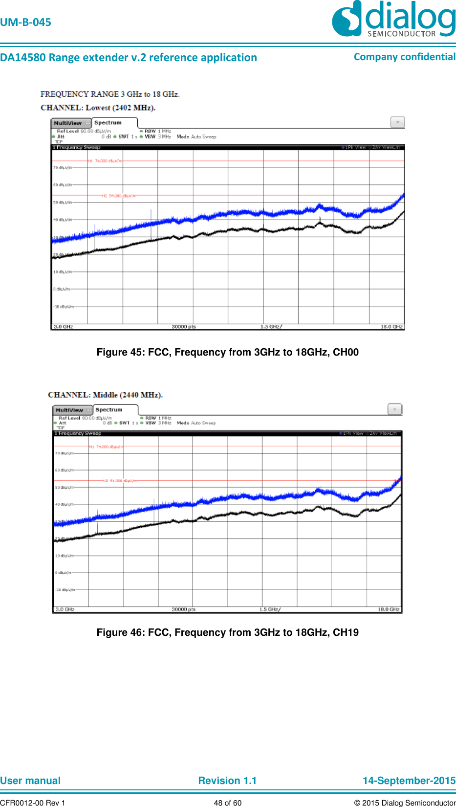
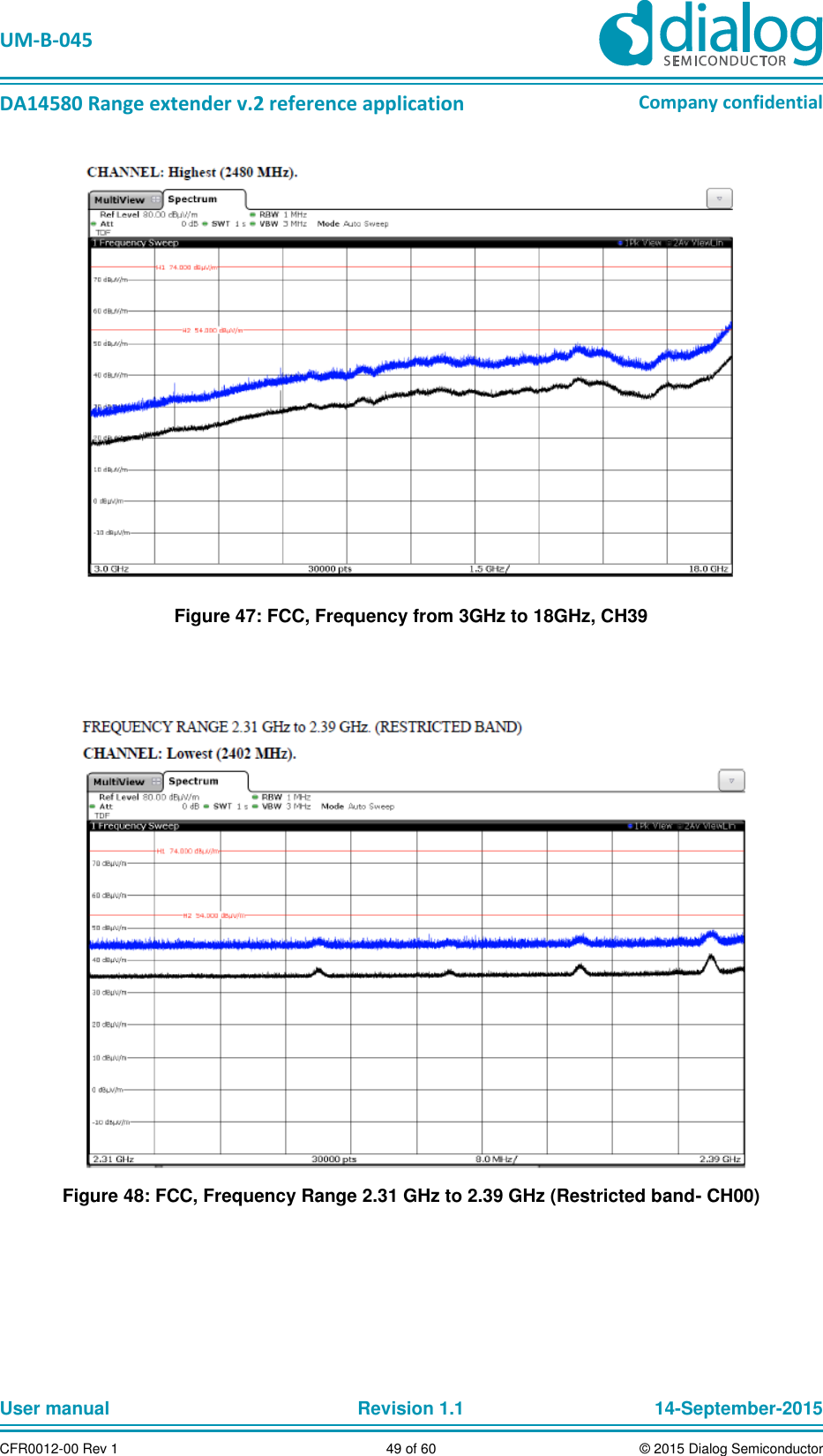
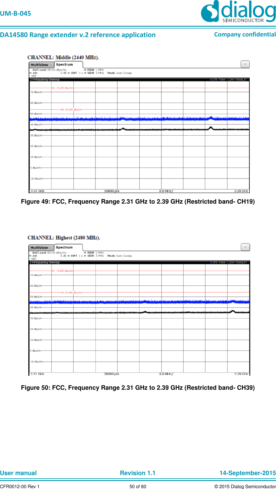
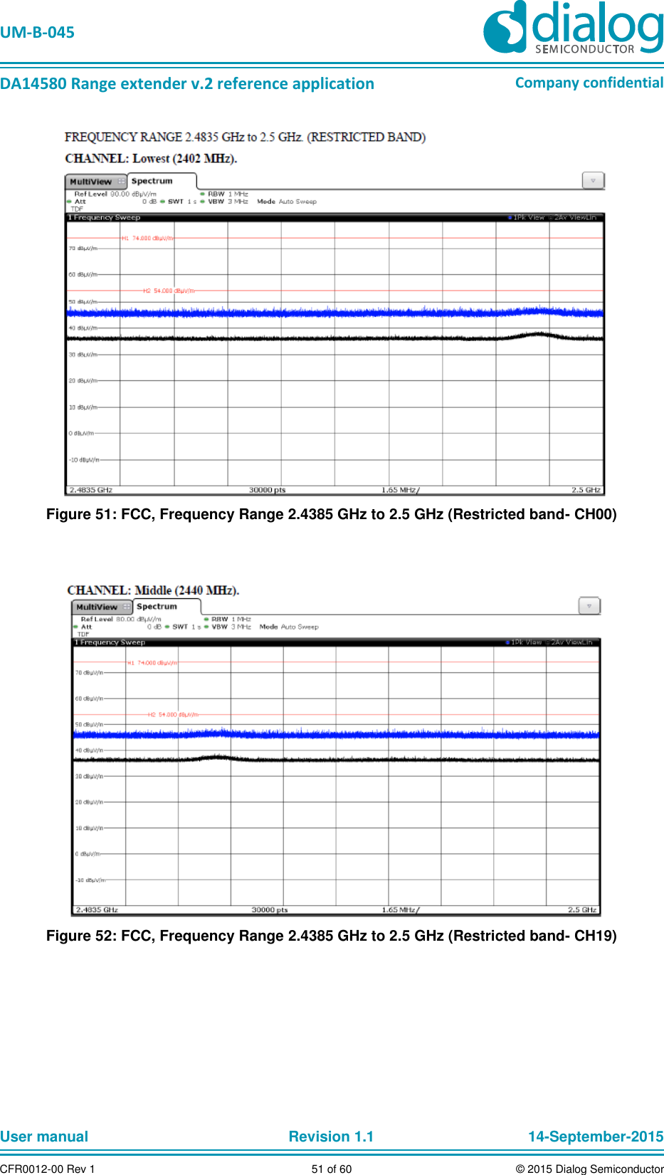
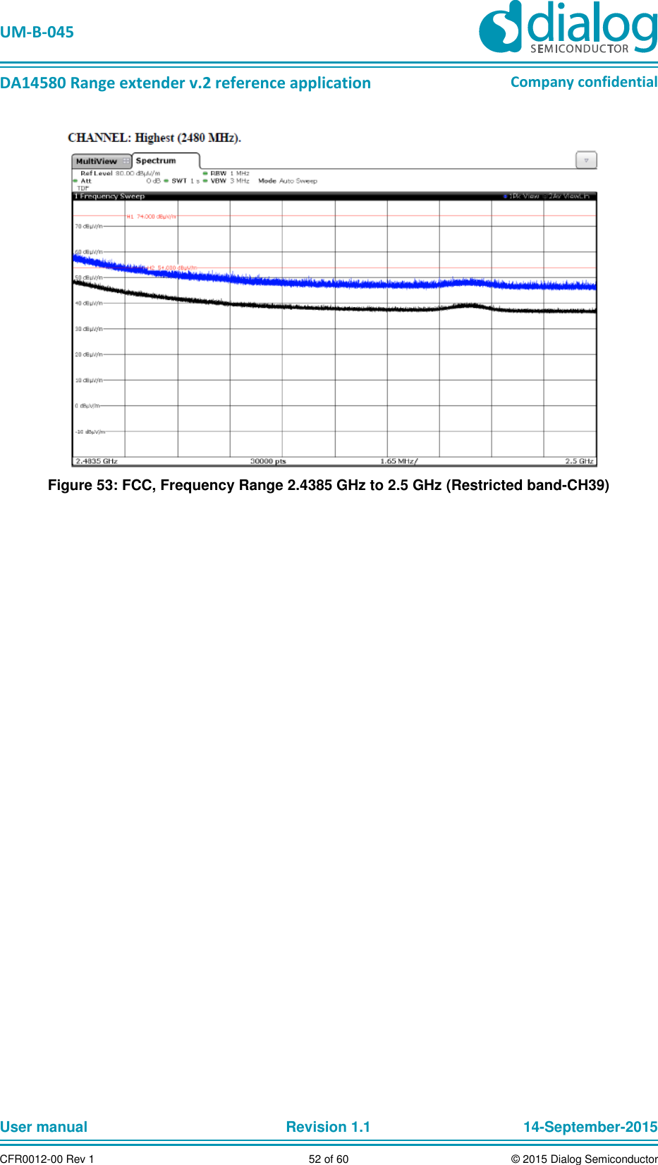
![UM-B-045 DA14580 Range extender v.2 reference application Company confidential User manual Revision 1.1 14-September-2015 CFR0012-00 Rev 1 16 of 60 © 2015 Dialog Semiconductor Table 3: BLE_CNTL2_REG (0x40000200) register specification In BLE_CNTL2_REG the port and the pins assignment order is defined. Only port 0 (P0_[0:7]) and port 1 (P1_[0:3]) of the chip can be utilized. DIAG0DIAG1DIAG2DiagOut[0]DiagOut[1]DiagOut[2]DiagOut[3]DiagOut[4]DiagOut[5]DiagOut[6]DiagOut[7] P0_0P0_1P0_2P0_3P0_4P0_5P0_6P0_7P1_0P1_1BLE DIAGNOSTIC BLE_DIAGCNTL_REG [DIAG0, DIAG1, DIAG2] BLE_CNTL2_REG (DIAGPORT_ REVERSE =1) ororBLE_CNTL2_REG (DIAGPORT_ SELECT =0 ) DIAG0DIAG1DIAG2DiagOut[0]DiagOut[1]DiagOut[2]DiagOut[3]DiagOut[4]DiagOut[5]DiagOut[6]DiagOut[7]P0_0P0_1P0_2P0_3P0_4P0_5P0_6P0_7P1_0P1_1BLE DIAGNOSTIC BLE_DIAGCNTL_REG [DIAG0, DIAG1, DIAG2] BLE_CNTL2_REG (DIAGPORT_ REVERSE =0 ) ororBLE_CNTL2_REG (DIAGPORT_ SELECT =0 ) Figure 7: Diagnostic port to pins assignment and register settings](https://usermanual.wiki/Dialog-Semiconductor/DA14580REXT/User-Guide-2869191-Page-16.png)