Dialog Semiconductor DA14580REXT BLE RF Module User Manual DA14580 Range extender v 2 reference application
Dialog Semiconductor BV BLE RF Module DA14580 Range extender v 2 reference application
User Manual

Company confidential
User manual
DA14580 Range extender v.2
reference application
UM-B-045
Abstract
This document describes the Bluetooth Range Extender v.2 module, based on the DA14580 SoC.
Target hardware: 580 RD QFN40 Module_RF PA_vC – Board Number: 078-56-C.

UM-B-045
DA14580 Range extender v.2 reference application
Company confidential
User manual
Revision 1.1
14-September-2015
CFR0012-00 Rev 1
2 of 60
© 2015 Dialog Semiconductor

UM-B-045
DA14580 Range extender v.2 reference application
Company confidential
User manual
Revision 1.1
14-September-2015
CFR0012-00 Rev 1
3 of 60
© 2015 Dialog Semiconductor
Contents
Contents .................................................................................................................................... 3
1 Terms and definitions ........................................................................................................... 8
2 References ........................................................................................................................... 8
3 Introduction ......................................................................................................................... 9
4 System overview .................................................................................................................. 9
Features ................................................................................................................................ 9 4.1
General description............................................................................................................. 10 4.2
Bluetooth SoC ..................................................................................................................... 11 4.3
RF front end ........................................................................................................................ 13 4.4
Radio front end control signals ............................................................................ 14 4.4.1
4.4.1.1 Radio front end control signals .......................................................... 14
4.4.1.2 Suggested pin assignment ................................................................. 17
Power amplifier .................................................................................................... 19 4.4.2
Low pass filter ....................................................................................................... 20 4.4.3
Antenna ................................................................................................................ 21 4.4.4
4.4.4.1 Range Extender v.2 on Interposer ..................................................... 21
4.4.4.2 Range Extender v.2 stand alone......................................................... 24
Power system and requirements ........................................................................................ 26 4.5
Trimming the 16MHz Xtal ................................................................................................... 26 4.6
PCBA .................................................................................................................................... 27 4.7
Development Mode-Peripheral Pin Mapping ..................................................................... 30 4.8
Software .............................................................................................................................. 32 4.9
5 Measurements ....................................................................................................................37
Basic performance measurements ..................................................................................... 37 5.1
Receiver sensitivity (conducted) .......................................................................... 37 5.1.1
5.1.1.1 Test description .................................................................................. 37
5.1.1.2 Test setup ........................................................................................... 37

UM-B-045
DA14580 Range extender v.2 reference application
Company confidential
User manual
Revision 1.1
14-September-2015
CFR0012-00 Rev 1
4 of 60
© 2015 Dialog Semiconductor
5.1.1.3 Test results ......................................................................................... 37
Transmitter output power (conducted) ............................................................... 39 5.1.2
5.1.2.1 Test description .................................................................................. 39
5.1.2.2 Test setup ........................................................................................... 39
5.1.2.3 Test results ......................................................................................... 39
Current consumption ........................................................................................... 41 5.1.3
5.1.3.1 Test setup ........................................................................................... 41
5.1.3.2 Advertisement mode ......................................................................... 41
5.1.3.3 Connection mode ............................................................................... 42
5.1.3.4 Extended sleep mode ......................................................................... 43
FCC/ ETSI Measurements .................................................................................................... 44 5.3
Emission limitation conducted (transmitter) ....................................................... 44 5.3.1
5.3.1.1 Test description .................................................................................. 44
5.3.1.2 Test setup ........................................................................................... 44
5.3.1.3 Test results ......................................................................................... 44
Emission limitation radiated (transmitter) ........................................................... 44 5.3.2
5.3.2.1 Test description .................................................................................. 44
5.3.2.2 Test setup ........................................................................................... 44
5.3.2.3 Test results ......................................................................................... 45
6 FCC/IC Certification and CE marking .....................................................................................53
Standards and conformity assessment ............................................................................... 53 6.1
FCC/IC Regulatory notices ................................................................................................... 53 6.2
1999/5/EC Directive regulatory notices ............................................................................. 54 6.3
7 Appendix A: Range Extender v.2 with SPI Data Flash .............................................................57
8 Revision history ...................................................................................................................59

UM-B-045
DA14580 Range extender v.2 reference application
Company confidential
User manual
Revision 1.1
14-September-2015
CFR0012-00 Rev 1
5 of 60
© 2015 Dialog Semiconductor
List of Figures and Tables
Figure 1: DA14580 Range Extender v.2 module .................................................................................... 9
Figure 2: Block diagram ....................................................................................................................... 10
Figure 3: Sky66111-11 Power Amplifier .............................................................................................. 11
Figure 4: DA14580 QFN40 SoC, Range Extender ver.2 module .......................................................... 12
Figure 5: RF front end signal paths ...................................................................................................... 13
Figure 6: RF front end schematic ........................................................................................................ 14
Figure 7: Diagnostic port to pins assignment and register settings .................................................... 16
Figure 8: The RF control signals ........................................................................................................... 18
Figure 9: Rising edge of Tx_En control signal ...................................................................................... 18
Figure 10: Detail from Tx_En to Rx_En signal ..................................................................................... 19
Figure 11: Low pass filter..................................................................................................................... 20
Figure 12: T- shaped, 3-poles, Low Pass Filter .................................................................................... 20
Figure 13: Simulation results of LPF response .................................................................................... 21
Figure 14: Range Extender v.2 on interposer ...................................................................................... 21
Figure 15: Antenna geometry on Range Extender v.2 ........................................................................ 22
Figure 16: Measured S11 paramater for IFA ....................................................................................... 22
Figure 17: Radiation diagram for the board placed vertically on the short edge ............................... 23
Figure 18: Radiation diagram for the board placed horizontally ........................................................ 23
Figure 19: Range Extender v.2 stand-alone ........................................................................................ 24
Figure 20: Radiation diagram for the board placed vertically on the short edge ............................... 24
Figure 21: Radiation diagram for the board placed horizontally ........................................................ 25
Figure 22: IFA antenna implementation ............................................................................................. 25
Figure 23: Current consumption for Advertisement frame ................................................................ 26
Figure 24: Top view of PCBA ............................................................................................................... 27
Figure 25: Schematic of DA14580 Range Extender v.2 Module .......................................................... 28

UM-B-045
DA14580 Range extender v.2 reference application
Company confidential
User manual
Revision 1.1
14-September-2015
CFR0012-00 Rev 1
6 of 60
© 2015 Dialog Semiconductor
Figure 26: DA14580/581/583 configuration settings for peripherals, periph_setup.h ...................... 31
Figure 27: Step 2 of adding app_range_extender ............................................................................... 32
Figure 28: Step 3a of adding app_range_extender ............................................................................. 32
Figure 29: Step 3b of adding app_range_extender ............................................................................. 33
Figure 30: Step 4a of adding app_range_extender ............................................................................. 33
Figure 31: Step 4b of adding app_range_extender ............................................................................. 34
Figure 32: Step 5a of adding app_range_extender ............................................................................. 34
Figure 33: Step 5b of adding app_range_extender ............................................................................. 35
Figure 34: Inserting app_range_extender in the production test tool ............................................... 36
Figure 35: Nominal conducted output power per channel ................................................................. 39
Figure 36: Peak conducted output power per channel ....................................................................... 40
Figure 37: Supplu current during an Advertisement frame ................................................................ 41
Figure 38: Supply current during a Connection frame ........................................................................ 42
Figure 39: Supply current during Extended Sleep mode ..................................................................... 43
Figure 40: Range Extender v.2 mounted on the interposer board for radiated measurements ........ 45
Figure 41: FCC, Frequency Range from 30MHz to 1 GHz, CH39 ......................................................... 46
Figure 42: FCC, Frequency from 1GHz to 3GHz, CH00 ........................................................................ 46
Figure 43: FCC, Frequency from 1GHz to 3GHz, CH19 ........................................................................ 47
Figure 44: FCC, Frequency from 1GHz to 3GHz, CH39 ........................................................................ 47
Figure 45: FCC, Frequency from 3GHz to 18GHz, CH00 ...................................................................... 48
Figure 46: FCC, Frequency from 3GHz to 18GHz, CH19 ...................................................................... 48
Figure 47: FCC, Frequency from 3GHz to 18GHz, CH39 ...................................................................... 49
Figure 48: FCC, Frequency Range 2.31 GHz to 2.39 GHz (Restricted band- CH00) ............................. 49
Figure 49: FCC, Frequency Range 2.31 GHz to 2.39 GHz (Restricted band- CH19) ............................. 50
Figure 50: FCC, Frequency Range 2.31 GHz to 2.39 GHz (Restricted band- CH39) ............................. 50
Figure 51: FCC, Frequency Range 2.4385 GHz to 2.5 GHz (Restricted band- CH00) ........................... 51
Figure 52: FCC, Frequency Range 2.4385 GHz to 2.5 GHz (Restricted band- CH19) ........................... 51

UM-B-045
DA14580 Range extender v.2 reference application
Company confidential
User manual
Revision 1.1
14-September-2015
CFR0012-00 Rev 1
7 of 60
© 2015 Dialog Semiconductor
Figure 53: FCC, Frequency Range 2.4385 GHz to 2.5 GHz (Restricted band-CH39) ............................ 52
Figure 54: Range Extender v.2 Module with external SPI Flash .......................................................... 58
Table 1: Electrical characteristics ........................................................................................................ 10
Table 2: BLE_ DIAGCNTL_REG (0x40000050) register specification ................................................... 15
Table 3: BLE_CNTL2_REG (0x40000200) register specification........................................................... 16
Table 4: Diagnostic port availability and settings for control pins ...................................................... 17
Table 5: Suggested pin assignment for extracting all RF control signals ............................................ 17
Table 6: Antenna gain Range Extender v.2 with interposer ................................................................ 22
Table 7: Antenna gain Range Extender v.2 stand-alone ..................................................................... 24
Table 8: Module Pin assignment ......................................................................................................... 27
Table 9: Bill of Materials ...................................................................................................................... 29
Table 10: Development/ testing mode pin mapping .......................................................................... 30
Table 11: Conducted Rx sensitivity ...................................................................................................... 38
Table 12: Tx output power .................................................................................................................. 40
Table 13: Peak current during Advertisement mode .......................................................................... 41
Table 14: Peak current during Connection mode ............................................................................... 42
Table 15: Average current in Extended Sleep mode ........................................................................... 43
Table 16: Conducted Tx harmonics at VBAT_3V = 3.0 V @ CH00, CH19, CH39 ....................................... 44

UM-B-045
DA14580 Range extender v.2 reference application
Company confidential
User manual
Revision 1.1
14-September-2015
CFR0012-00 Rev 1
8 of 60
© 2015 Dialog Semiconductor
1 Terms and definitions
BLE Bluetooth Low Energy
BOM Bill Of Materials
DUT Device Under Test
ERP Effective Radiated Power
FW Firmware
LPF Low Pass Filter
PA Power Amplifier
PCBA Printed Circuit Board Assembled
PCB Printed Circuit Board
RF Radio Frequency
SoC System on Chip
SPDT Single Pole Double Throw
2 References
1. DA14580 Low Power Bluetooth Smart SoC, Datasheet, Dialog Semiconductor
2. SKY66111-11 Datasheet
3. AN-B-020 End product testing and programming guidelines.(This document is susceptible to be replaced)
4. UM-B-012 DA14580/581/583 Creation of a secondary boot loader
UM-B-045
DA14580 Range extender v.2 reference application
Company confidential
User manual
Revision 1.1
14-September-2015
CFR0012-00 Rev 1
9 of 60
© 2015 Dialog Semiconductor
3 Introduction
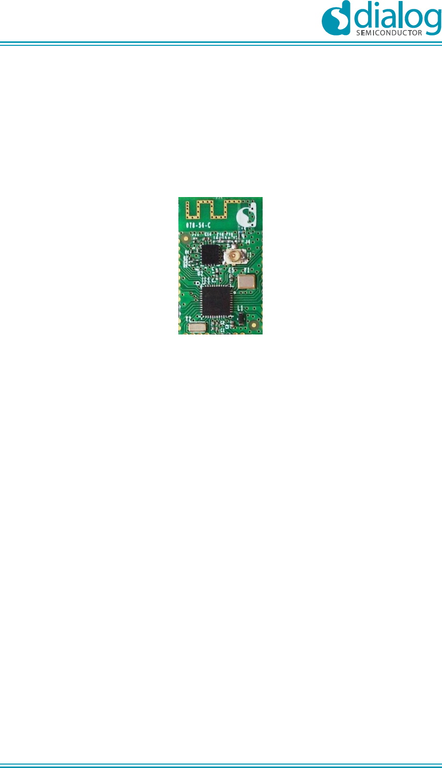
The DA14580 Range Extender v.2 module design is based on the Dialog Semiconductor DA14580
BLE Smart SoC, where enhanced RF transmitted power is presented. This module serves as
reference design to potential customers requesting BLE functionality with Nominal RF Output power
up to +9.3 dBm (Peak RF Output Power +9.8 dBm). From physical perspective, the module is a two
layer PCBA where the digital and power interfaces of the DA14580 are accessible to the user. This
document presents the system, technical specifications, physical dimensions and test results.
Figure 1: DA14580 Range Extender v.2 module
4 System overview
Features 4.1
■ Highly integrated Dialog Semiconductor DA14580 Bluetooth ® Smart SoC
■ Module can be used as either stand-alone or as a data pump on a system with an external
processor
■ Module satisfies all Bluetooth requirements
■ No external crystal or additional passive components are required for module operation, as the
module is equipped with two crystal oscillators one at 16MHz (XTAL16M) and a second at
32.738KHz (XTAL32K). The 32.738 KHz is used as the clock of Extended/ Deep Sleep modes.
■ Access to processor via JTAG, SPI, UART or I2C
■ 22 GPIOs available on module at a 1.27 mm pitch, suitable for keyboard designs
■ Operating voltage: 2.4 V to 3.3 V. Suitable for operation from a single coin cell battery.
■ On-board printed inverted F-type antenna (Figure 1)
■ RF connector for conducted measurements( Figure 1)
■ Up to +9.3 dBm Nominal Maximum Output Power (+9.8dBm Peak Maximum Output Power).
■ Rx sensitivity: better than -90 dBm
■ Supply current:
-Tx : less than 17 mA peak current @ 3.0 V
-Rx: less than 6 mA peak current @ 3.0 V
-Extended - Sleep current: less than 1.6A @ 3.0 V
■ 15.25 mm x 24 mm, 37 pins, two layer PCBA
■ Operating temperature: –40 ºC to +85 ºC
■ Test FW based on DA14580_581_583_SDK_3.0.10.1
UM-B-045
DA14580 Range extender v.2 reference application
Company confidential
User manual
Revision 1.1
14-September-2015
CFR0012-00 Rev 1
10 of 60
© 2015 Dialog Semiconductor
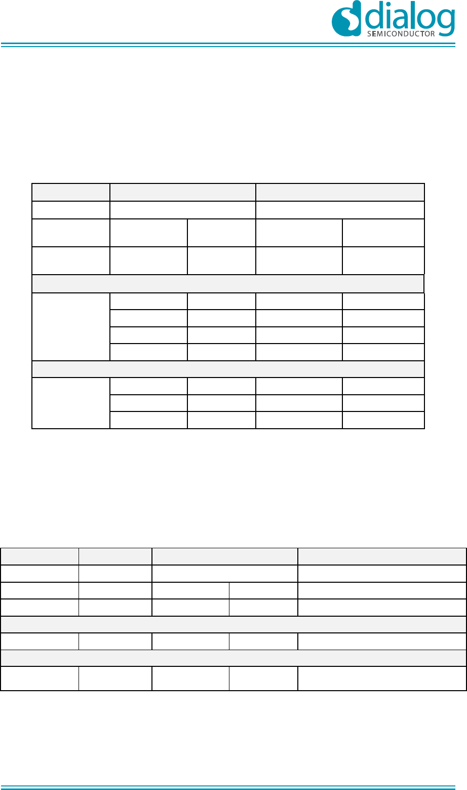
Table 1: Electrical characteristics
Characteristic
Value
Comments
Battery voltage (VBAT_3V)
2.4 V to 3.3 V
Specification tested at typical
voltage of 3.0 V
Operating frequency range
2400 MHz to 2483.5 MHz
Conducted output power
+9.3 dBm
VBAT_3V = 3 V, TA = +15 to +35 °C
Maximum bypass loss
0.6 dB
VBAT_3V = 3 V, TA = +15 to +35 °C
Receiver sensitivity
Better than -90 dBm
VBAT_3V = 3 V, TA = +15 to +35 °C
Peak Tx current
<17mA
Tx Power = +9.3 dBm,
VBAT_3V = 3 V, TA = +15 to +35 °C
Peak extended-sleep current
<1.6A
VBAT_3V = 3 V, TA = +15 to +35 °C
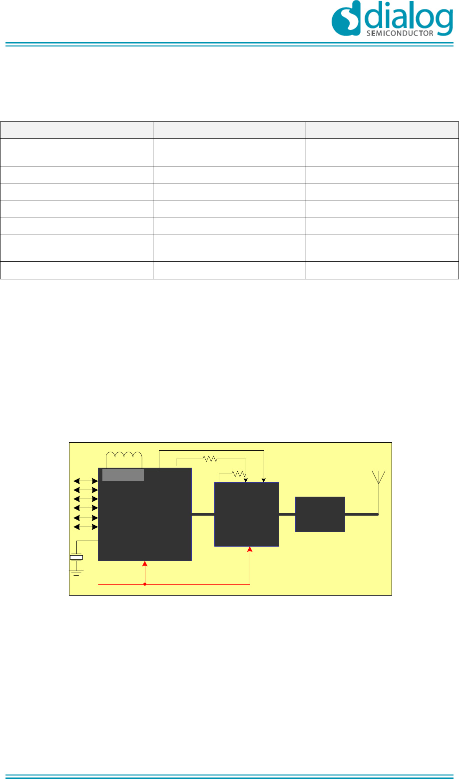
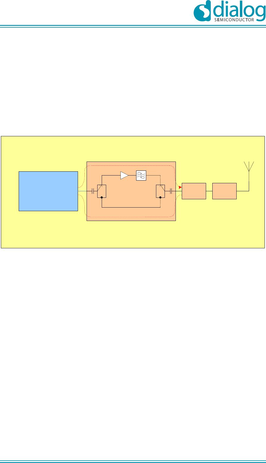
General description 4.2
The system consists of the DA14580 Bluetooth Low power SoC, the SKY6611-11 Front-end module
and a discrete low pass filter. The radio front end is connected to a PCB trace antenna as Figure 2
shows.
The power amplifier is controlled by the CTRL1 and CTRL2 signals. CTRL1 is generated from pin
P0_3 and CTRL2 is generated from P0_2 of the DA14580. On pin P0_3 and pin P0_2 the internal
Radio_TXEN and Radio_RXEN signals are software allocated.
DA14580
QFN40 Sky6611-11 Discrete
LPF
cRx
Bias
P0_2 P0_3
buck
VBAT_3V
gpios RBIAS
cTx
CTRL1
CTRL2
Figure 2: Block diagram
The amplifier circuit is the SKY66111-11 from Skyworks. The CTX pin is used as the TX control
signal and amplifier bias voltage. CTX pin is connected to the amplifier BIAS pin via resistor RBIAS.
The resistor value is adjusted in order to get a Nominal RF Output Power of +9.3 dBm. More
information for the power output adjustment can be found in Sky66111-11 datasheet2.
UM-B-045
DA14580 Range extender v.2 reference application
Company confidential
User manual
Revision 1.1
14-September-2015
CFR0012-00 Rev 1
11 of 60
© 2015 Dialog Semiconductor
Figure 3: Sky66111-11 Power Amplifier
Bluetooth SoC 4.3
The DA14580 integrated circuit has a fully integrated radio transceiver and baseband processor for
Bluetooth ® Smart. It can be used as an application processor as well as a data pump in systems
with an external processor.
The DA14580 contains an embedded One-Time-Programmable (OTP) memory for storing Bluetooth
profiles as well as custom application code. The qualified Bluetooth® Smart protocol stack, which is
stored in a dedicated ROM, and the customer application software which is stored in system RAM,
run on the embedded ARM Cortex M0 processor. Low leakage Retention RAM is used to store
sensitive data and connection information while in Deep Sleep mode.
The Radio Transceiver implements the RF part of the Bluetooth Smart protocol. Together with the
Bluetooth 4.0 PHY layer, it provides a 93 dB RF link budget for reliable wireless communication. All
RF blocks are supplied by on-chip low drop out regulators (LDOs). The RF port is single ended 50 ,
so no external balun is required.
The DA14580 has dedicated hardware for the Link Layer implementation of Bluetooth® Smart and
interface controllers for enhanced connectivity capabilities.
The reset line of the DA14580 (pin RST) is active high. On this module the RST pin is available on
module pin 21.
Main debug port for the DA14580 is the JTAG. JTAG consists of two signals, SWDIO and SWCLK.
The frequency tolerance specification for BLE is 50 ppm. In order to compensate ageing and offset
effects, an external crystal shall have an accuracy of ±15 ppm or better. The DA14580 crystal (Y1)
has a fundamental frequency of 16 MHz and load capacitance not higher than 10 pF. The crystal is
located on the module itself. Also, an internal programmable capacitance bank is available in the
DA14580. In this way, the crystal oscillator frequency can be tuned.
For sleep mode the on chip RCX oscillator is utilized. In addition, a 32 kHz crystal (Y2) with a
tolerance of 50 ppm (500 ppm max) can be assembled on the module. The crystal load capacitance
shall not be higher than 10 pF.
The external digital interfaces available for the module are:
● 2 UARTs with hardware flow control up to 1 MBd
● SPI interface
● I2C bus at 100 kHz, 400 kHz
UM-B-045
DA14580 Range extender v.2 reference application
Company confidential
User manual
Revision 1.1
14-September-2015
CFR0012-00 Rev 1
12 of 60
© 2015 Dialog Semiconductor
● 3-axis capable Quadrature Decoder
There is also a 4-channel 10-bit ADC available externally to the module.
The module includes 22 GPIOs (including JTAG signals) that are available externally. The interfaces
are multiplexed with the GPIOs and can be enabled by appropriate programming.
The DA14580 is equipped with a DC-DC converter that can be configured as either Buck or Boost.
For this module, the DC-DC converter is configured as a Buck converter (C5, C2, L1, C3).
The DA14580 is available in three packages: WLCSP34, QFN40 and QFN48. In this reference
application the QFN40 has been used.
Figure 4: DA14580 QFN40 SoC, Range Extender ver.2 module
UM-B-045
DA14580 Range extender v.2 reference application
Company confidential
User manual
Revision 1.1
14-September-2015
CFR0012-00 Rev 1
13 of 60
© 2015 Dialog Semiconductor
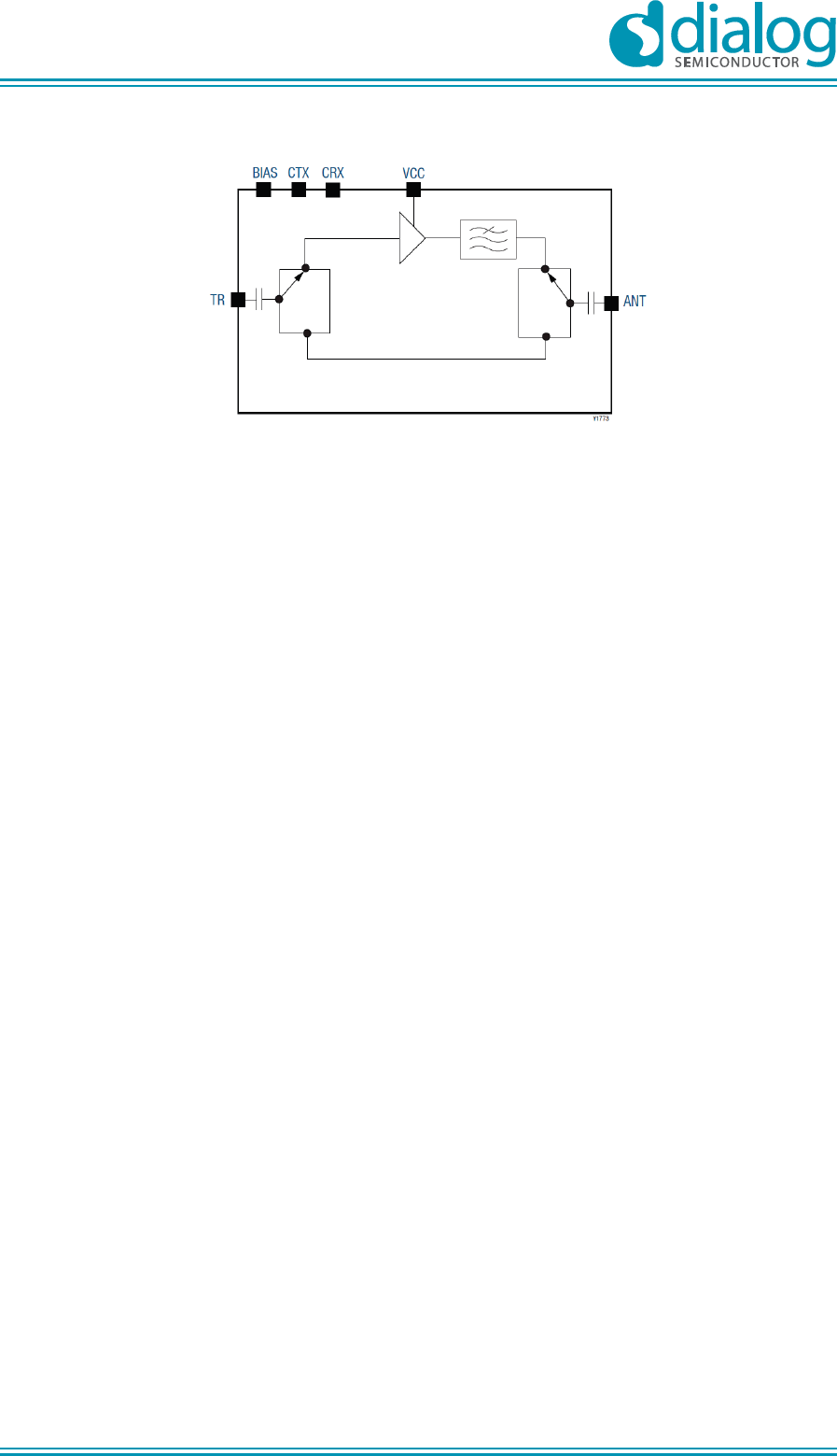
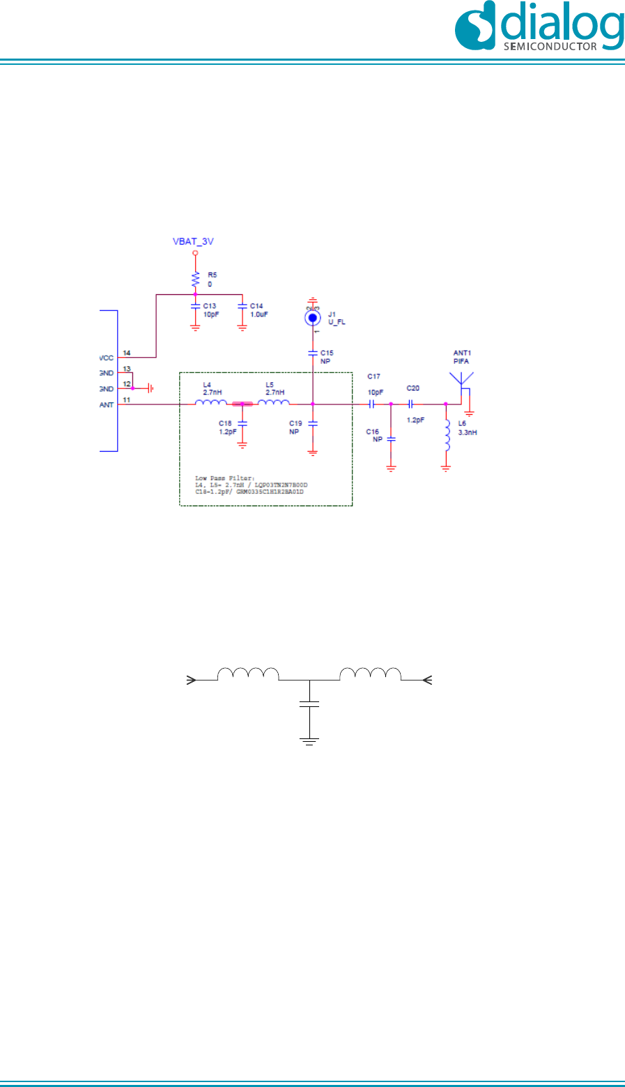
RF front end 4.4
This part of the design is implementing the amplification of the RF transmitted signal while the
transmitted harmonics as well as the Tx spurious emissions remain within the FCC/ETSI
specification.
The operation of the RF front end is controlled by the DA14580. There are two RF paths: one
through the amplifier and one bypass path. The amplifier path is enabled during transmission. The
RF signal passes through the PA, the low pass filter and the RF matching network. In the bypass
path, the RF signal received at the antenna is driven directly to the BLE transceiver.
DA14580
QFN40
BTLE SoC
Low Pass
Filter Matching
circuit
Amplifier
SKY66111-11
Amplifier bypass path
Power Amplifier Path
RFIOP
Figure 5: RF front end signal paths
UM-B-045
DA14580 Range extender v.2 reference application
Company confidential
User manual
Revision 1.1
14-September-2015
CFR0012-00 Rev 1
14 of 60
© 2015 Dialog Semiconductor
Figure 6: RF front end schematic
Radio front end control signals 4.4.1
4.4.1.1 Radio front end control signals
In general, three different radio control signal can be extracted from DA14580:
- extrc_txen, it can be used as Tx_En control signal of the RF front end.
- extrc_rxen or radcntl_rxen radio. Both signals are of the same duration. They can be used
as Rx_En control signals for the RF front end.
- event_in_process that can be used for wlan co-existence signal.
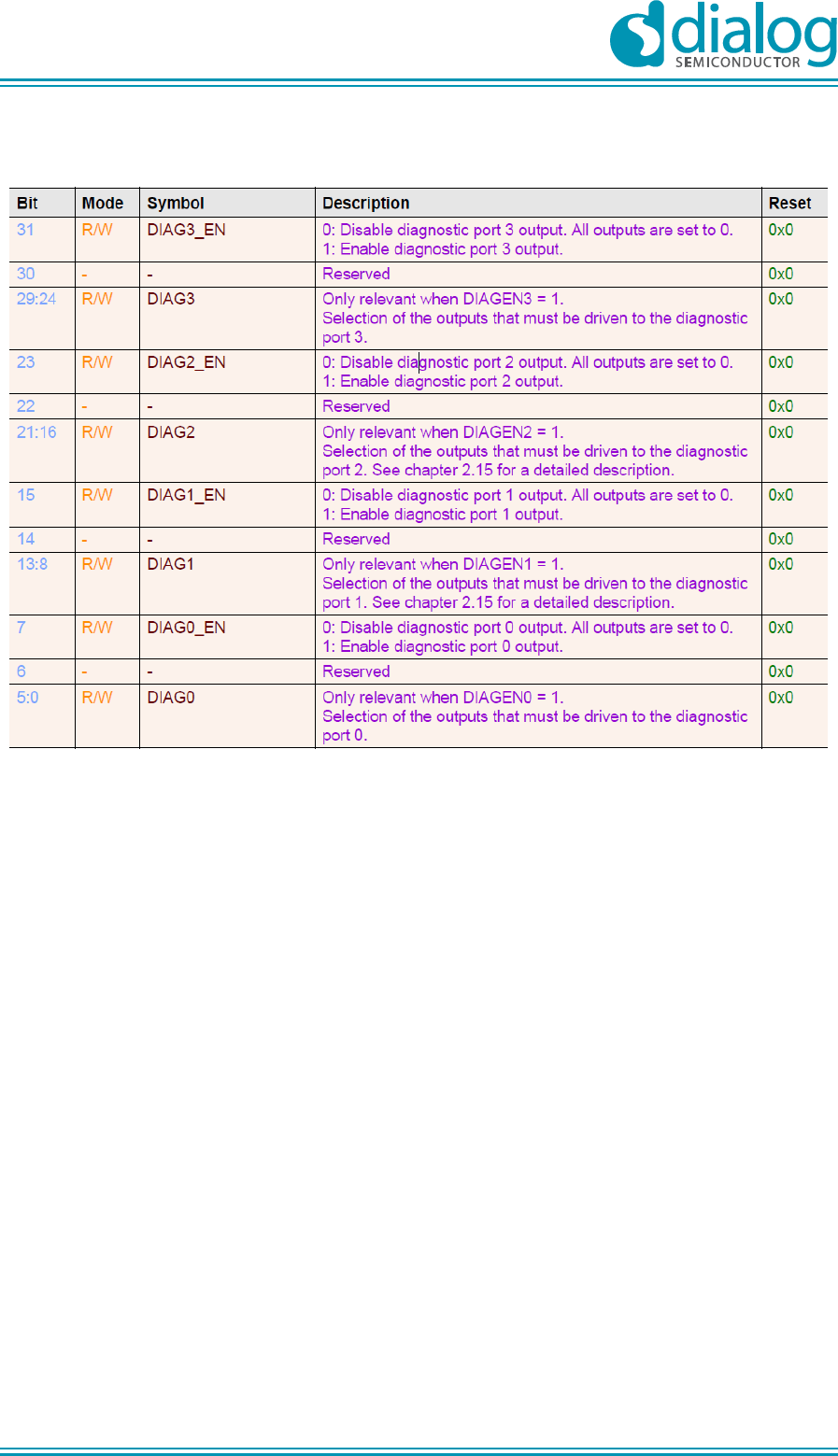
The signals are extracted by using the BLE diagnostic port. Two registers need to be programmed:
- BLE_DIAGCNTL_REG where it is defined which signals will be extracted from each port.
Register specification of BLE_ DIAGCNTL_REG :
UM-B-045
DA14580 Range extender v.2 reference application
Company confidential
User manual
Revision 1.1
14-September-2015
CFR0012-00 Rev 1
15 of 60
© 2015 Dialog Semiconductor
Table 2: BLE_ DIAGCNTL_REG (0x40000050) register specification
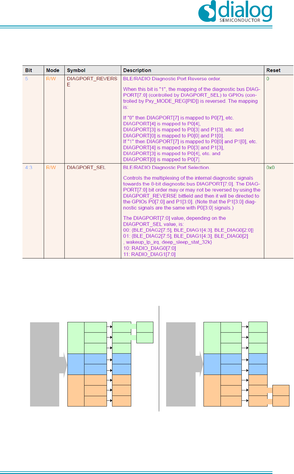
- BLE_CNTL2_REG where the BLE diagnostic port is enabled and the straight or reverse pin
assignment is defined. This function is controlled by two register bit-fields, DIAGPORT_SEL
and DIAGPORT_REVERSE. Description presented below on Table 3.
UM-B-045
DA14580 Range extender v.2 reference application
Company confidential
User manual
Revision 1.1
14-September-2015
CFR0012-00 Rev 1
16 of 60
© 2015 Dialog Semiconductor
Table 3: BLE_CNTL2_REG (0x40000200) register specification
In BLE_CNTL2_REG the port and the pins assignment order is defined. Only port 0 (P0_[0:7]) and
port 1 (P1_[0:3]) of the chip can be utilized.
DIAG0
DIAG1
DIAG2
DiagOut[0]
DiagOut[1]
DiagOut[2]
DiagOut[3]
DiagOut[4]
DiagOut[5]
DiagOut[6]
DiagOut[7] P0_0
P0_1
P0_2
P0_3
P0_4
P0_5
P0_6
P0_7
P1_0
P1_1
BLE
DIAGNOSTIC
BLE_DIAGCNTL_REG
[DIAG0, DIAG1, DIAG2] BLE_CNTL2_REG
(DIAGPORT_ REVERSE =1)
or
or
BLE_CNTL2_REG
(DIAGPORT_ SELECT =0 )
DIAG0
DIAG1
DIAG2
DiagOut[0]
DiagOut[1]
DiagOut[2]
DiagOut[3]
DiagOut[4]
DiagOut[5]
DiagOut[6]
DiagOut[7]
P0_0
P0_1
P0_2
P0_3
P0_4
P0_5
P0_6
P0_7
P1_0
P1_1
BLE
DIAGNOSTIC
BLE_DIAGCNTL_REG
[DIAG0, DIAG1, DIAG2] BLE_CNTL2_REG
(DIAGPORT_ REVERSE =0 )
or
or
BLE_CNTL2_REG
(DIAGPORT_ SELECT =0 )
Figure 7: Diagnostic port to pins assignment and register settings
UM-B-045
DA14580 Range extender v.2 reference application
Company confidential
User manual
Revision 1.1
14-September-2015
CFR0012-00 Rev 1
17 of 60
© 2015 Dialog Semiconductor
For having all pins extracted in parallel, a combination of register setting and pin availability must be
arranged. For example it is preferable to avoid assigning P0_4 and P0_5 to RF control signals. P0_4
and P0_5 are used for UART ports in testing and production tests.
The available pins are presented below:
Table 4: Diagnostic port availability and settings for control pins
Function
Diagnostic port settings
DA14580 assigned Pins
BLE_DIAGCNTL_REG
BLE_CNTL2_REG
DIAG port
DIAGx
DIAGPORT_
REVERSE = 0
DIAGPORT_
REVERSE = 1
Tx_Enable
DIAG1
0x28
P0_3
P0_4
Rx_Enable
DIAG1
0x28
P0_4
P0_3
DIAG2
0x08
P0_5
P0_2
DIAG2
0x0c
P0_6
P0_1, P1_1
DIAG0
0x1F
P0_2
P0_5
Wlan coexist
DIAG2
0x08
P0_7
P0_0, P1_0
DIAG2
0x0D
P0_7
P0_0, P1_0
DIAG2
0x1F
P0_6
P0_1, P1_1
4.4.1.2 Suggested pin assignment
A suggested pin assignment for extracting all rf control signals at the same time is presented below:
Table 5: Suggested pin assignment for extracting all RF control signals
function
Signal used
Diagnostic port settings
DA14580 assigned Pins
BLE_DIAGCNTL_REG
BLE_CNTL2_REG
DIAG port
DIAGx
DIAGPORT_ REVERSE = 0
PA_Tx Enable
extrc_txen
DIAG1
0x28
P0_3
PA_Rx Enable
radcntl_rxen
DIAG0
0x1F
P0_2
Wlan coexist
event_in_
process
DIAG2
0x08
P0_7
For more options on the pin assignment please read paragraph 4.8: Development mode-peripheral
pin mapping.
UM-B-045
DA14580 Range extender v.2 reference application
Company confidential
User manual
Revision 1.1
14-September-2015
CFR0012-00 Rev 1
18 of 60
© 2015 Dialog Semiconductor
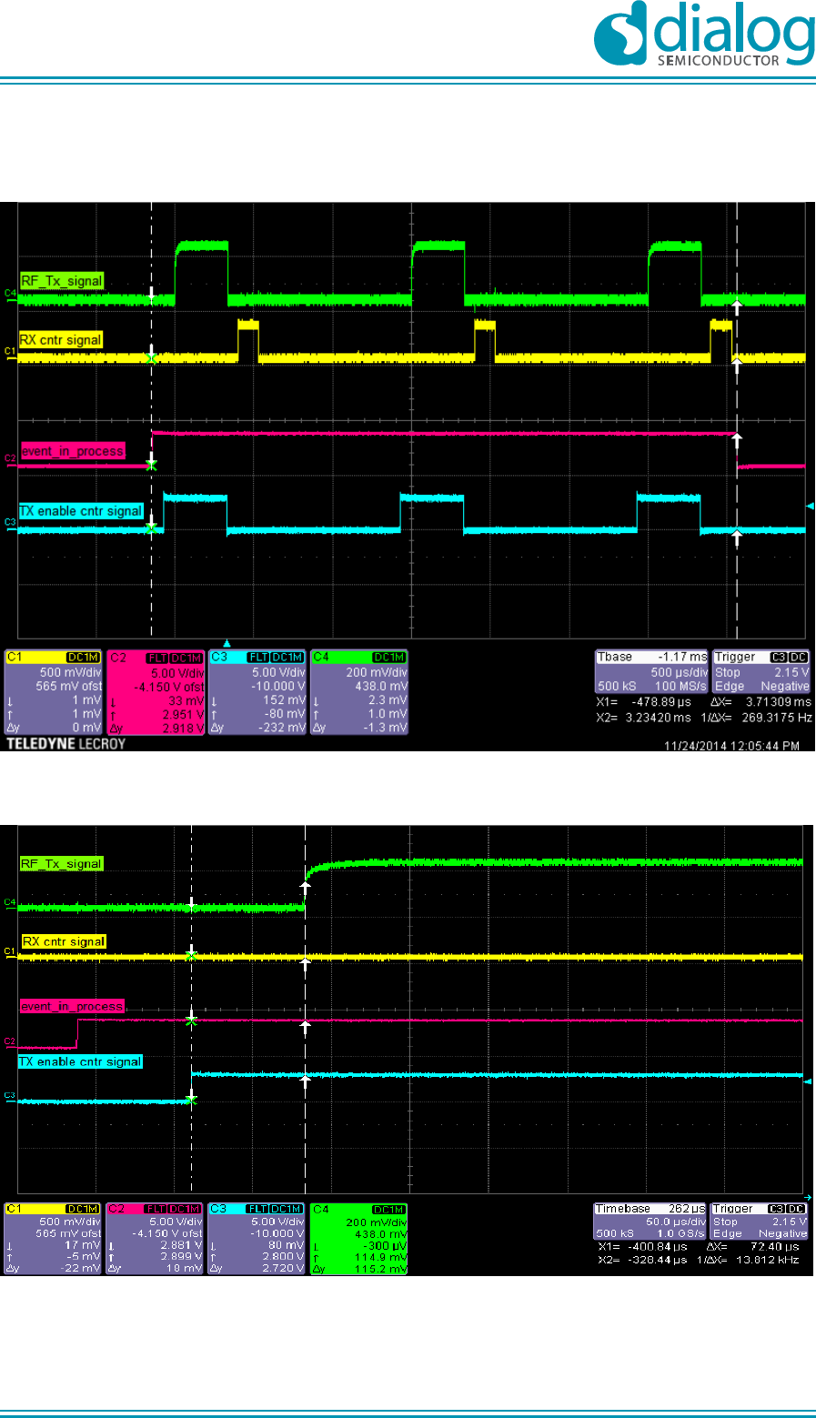
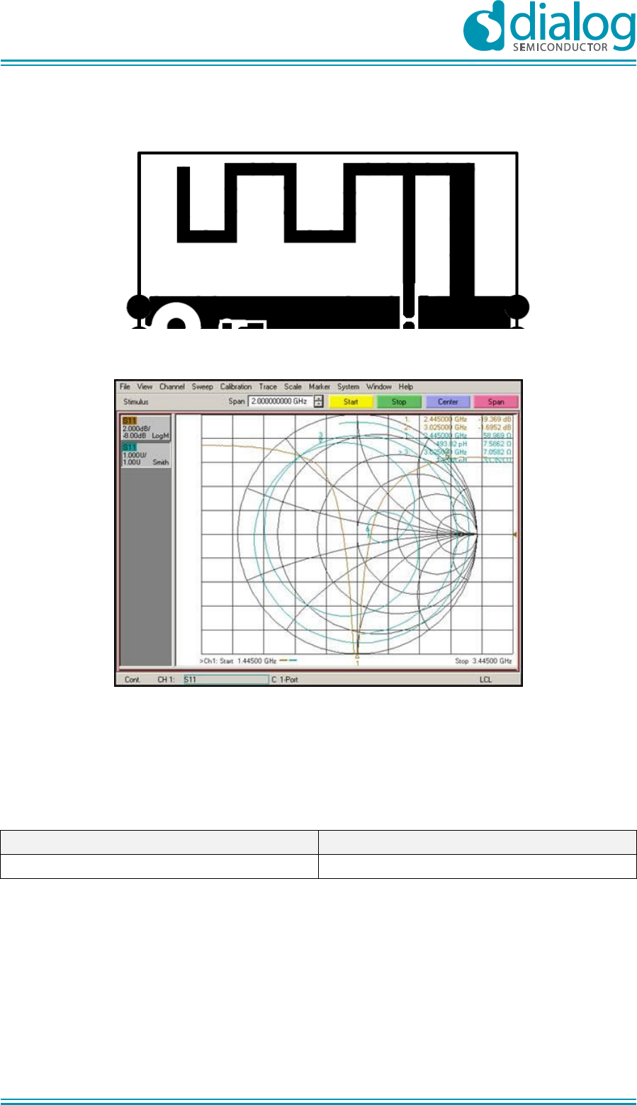
Below, screenshots from the radio control signals during operation are presented. The proximity
reporter_fh application was used.
Figure 8: The RF control signals
Figure 9: Rising edge of Tx_En control signal
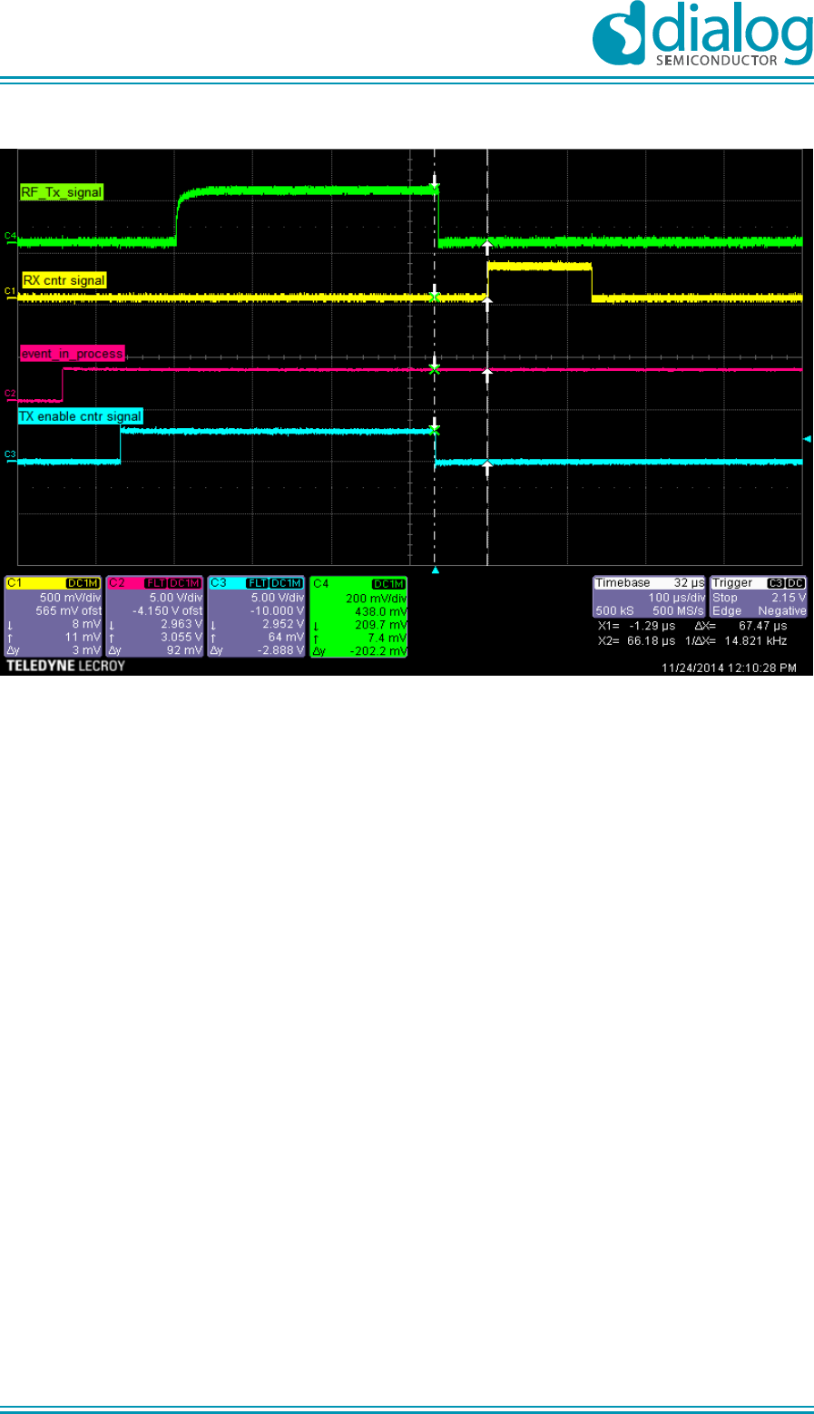
UM-B-045
DA14580 Range extender v.2 reference application
Company confidential
User manual
Revision 1.1
14-September-2015
CFR0012-00 Rev 1
19 of 60
© 2015 Dialog Semiconductor
Figure 10: Detail from Tx_En to Rx_En signal
Power amplifier
4.4.2
The amplifier circuit is the SKY66111-112 from Skyworks. The VBIAS pin is connected to the bias
voltage via resistor R7. The resistor value is adjusted so that the +9.3 dBm output power is achieved
at maximum 16.15 mA current consumption.
There are two Low Pass Filters options for the power amplifier. The first one is at the input of the
Skyworks amplifier and is formed by C6, C7 and L3 and the second is at the output of the Skyworks
amplifier and is formed by L4, L5, C18 and C19. The second LPF is used in the current design.
The power amplifier is supplied from pin VBAT_3V directly.
UM-B-045
DA14580 Range extender v.2 reference application
Company confidential
User manual
Revision 1.1
14-September-2015
CFR0012-00 Rev 1
20 of 60
© 2015 Dialog Semiconductor
Low pass filter 4.4.3
The low pass filter is placed after the amplifier matching network in order to suppress the harmonics
generated due to the amplifier’s nonlinearity. The filter presents low losses in the 2.4 GHz to 2.5 GHz
frequency range (max. loss: 0.5 dB). The ripple on the pass band was chosen equal to 0.1dB.
Figure 11: Low pass filter
RFPA ANT
2n7
1p2
2n7
Figure 12: T- shaped, 3-poles, Low Pass Filter
The filter is a T- type Chebyshev 3rd order low pass filter. The filter configuration is presented in
Figure 12.
Component value:
- 2,7nH : LQG15HN2N7S02 / Murata
- 1.2pF: GRM1555C1H1R2CZD1/ Murata
Frequency response measurements are presented in Figure 13 below.
UM-B-045
DA14580 Range extender v.2 reference application
Company confidential
User manual
Revision 1.1
14-September-2015
CFR0012-00 Rev 1
21 of 60
© 2015 Dialog Semiconductor
DB(S(S2,1))
DB(S(S1,2))
Freq
(GHz)
S(2,2)
S(1,1)
Freq
0.1 to 13.00 GHz
Figure 13: Simulation results of LPF response
Antenna 4.4.4
4.4.4.1 Range Extender v.2 on Interposer
The antenna is a printed Inverted F Antenna (IFA). The antenna was designed according to the size
of the module and the available antenna space (15.24 mm x 24 mm). The measurements for the
characterization of the antenna radiation pattern were performed with Range Extender v.2 module
mounted on an interposer board. The matching components values for the antenna measurement
are: C20= 1.2pF and L6=3.3nH.
Figure 14: Range Extender v.2 on interposer
UM-B-045
DA14580 Range extender v.2 reference application
Company confidential
User manual
Revision 1.1
14-September-2015
CFR0012-00 Rev 1
22 of 60
© 2015 Dialog Semiconductor
Figure 15: Antenna geometry on Range Extender v.2
Figure 16: Measured S11 paramater for IFA
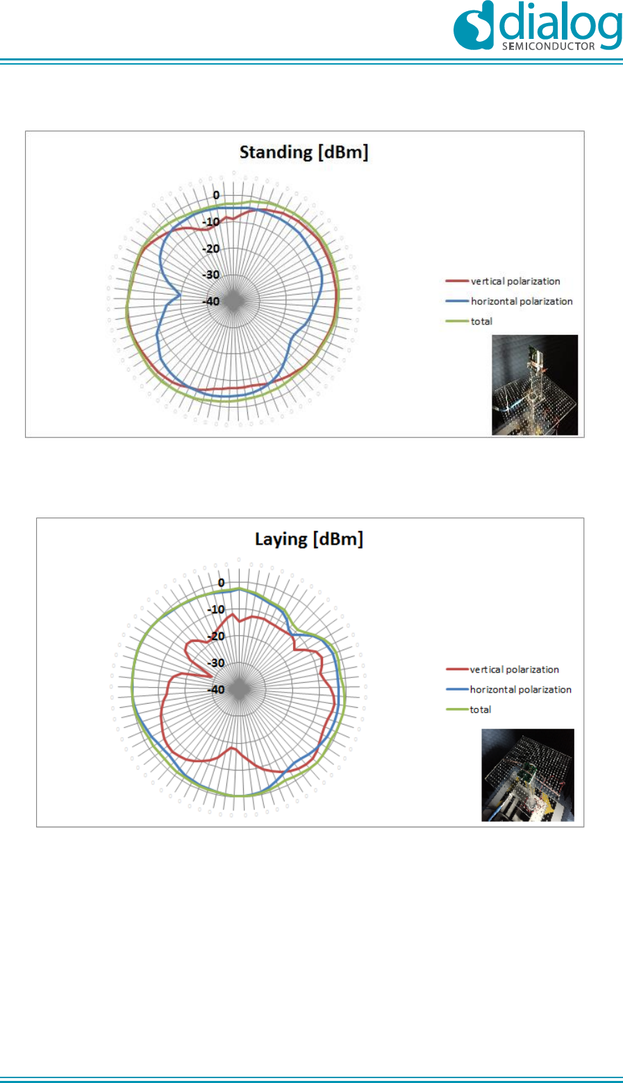
Gain measurements were performed in an anechoic chamber. The maximum gain was measured at
0 dBi.
Table 6: Antenna gain Range Extender v.2 with interposer
Parameter
G (dBi)
Maximum gain
0
UM-B-045
DA14580 Range extender v.2 reference application
Company confidential
User manual
Revision 1.1
14-September-2015
CFR0012-00 Rev 1
23 of 60
© 2015 Dialog Semiconductor
Figure 17: Radiation diagram for the board placed vertically on the short edge
Figure 18: Radiation diagram for the board placed horizontally
UM-B-045
DA14580 Range extender v.2 reference application
Company confidential
User manual
Revision 1.1
14-September-2015
CFR0012-00 Rev 1
24 of 60
© 2015 Dialog Semiconductor
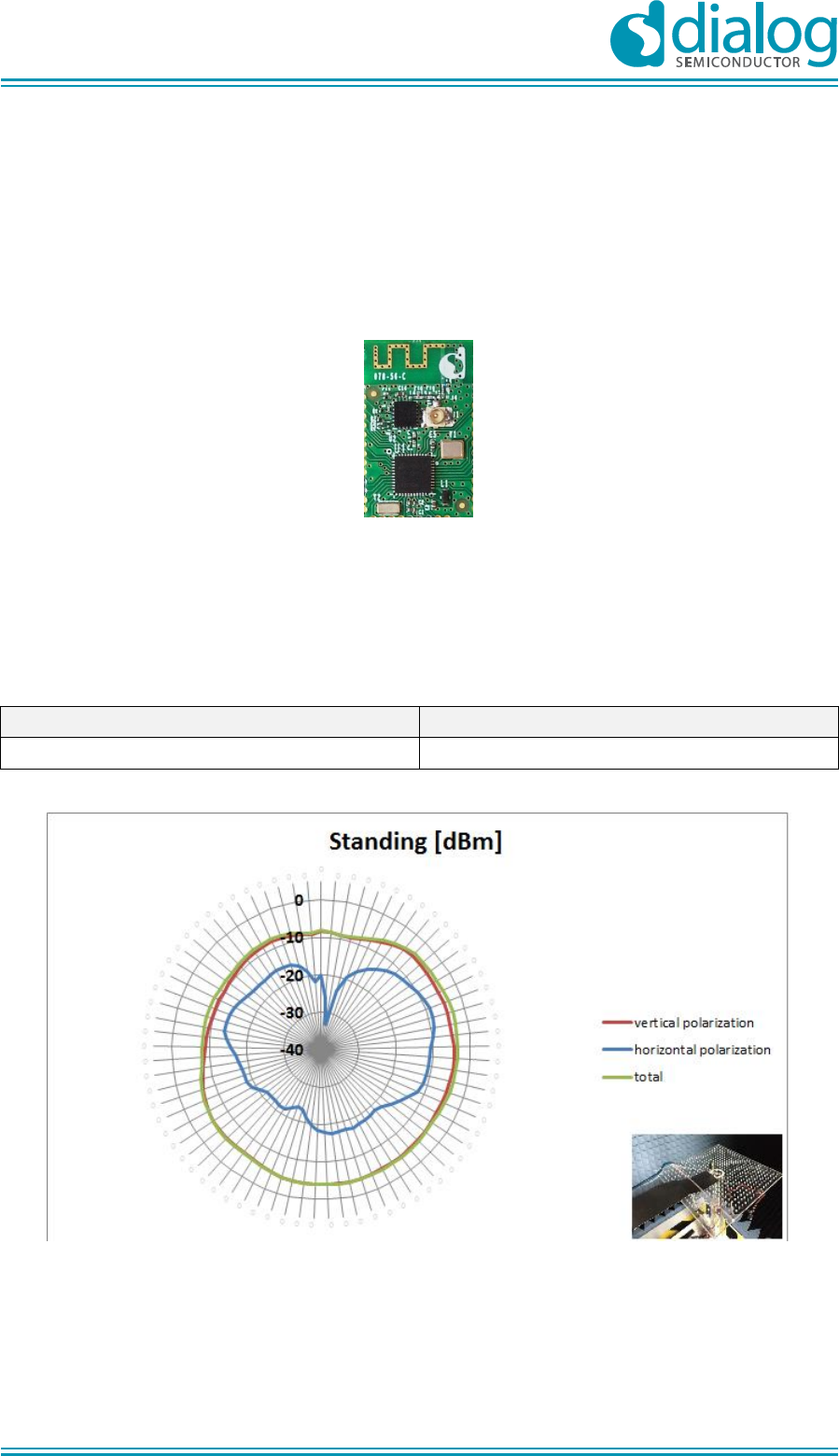
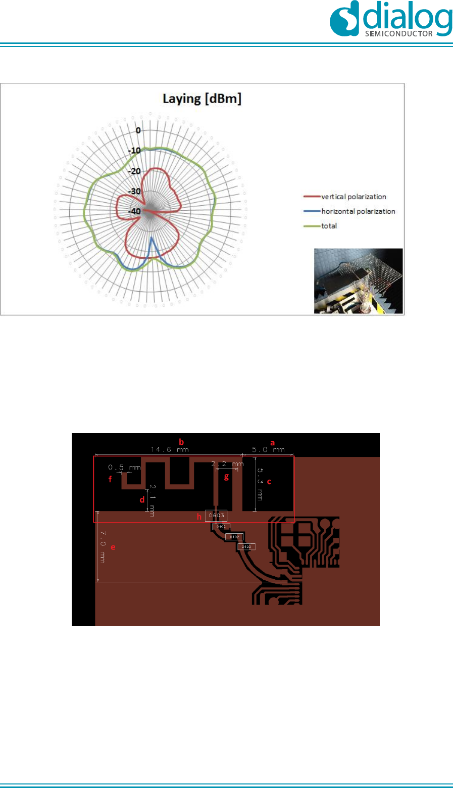
4.4.4.2 Range Extender v.2 stand alone
Measurements for the characterization of the antenna radiation pattern were also performed with
Range Extender v.2 not soldered on interposer. In this case the matching components values differ
from the values of the module on the interposer. The matching values of the components are: C20=
1.2pF and C16=1pF.
Figure 19: Range Extender v.2 stand-alone
Gain measurements were performed in an anechoic chamber. The maximum gain was measured at
-10 dBi.
Table 7: Antenna gain Range Extender v.2 stand-alone
Parameter
G (dBi)
Maximum gain
-10
Figure 20: Radiation diagram for the board placed vertically on the short edge
UM-B-045
DA14580 Range extender v.2 reference application
Company confidential
User manual
Revision 1.1
14-September-2015
CFR0012-00 Rev 1
25 of 60
© 2015 Dialog Semiconductor
Figure 21: Radiation diagram for the board placed horizontally
The stand-alone board presents lower antenna gain than the board mounted on the interposer. This
is explained due the small ground size of the board. It is recommended for Range Extender v.2 to be
mounted on a pcb with bigger ground surface or when embedded to a new design to follow the
dimensions in Figure 22.
Figure 22: IFA antenna implementation
The dimensions above are given for a typical FR1 PCB substrate, 1mm thick. The antenna length is
adjusted for resonance including a 1mm plastic enclosure placed in contact with the PCB antenna.
The red outline indicates the antenna footprint, i.e. required allocation of PCB space. The footprint of
the antenna is available per request in dxf format.
Legend (Figure 22):
Clearance between antenna arm and GND plane right a.
UM-B-045
DA14580 Range extender v.2 reference application
Company confidential
User manual
Revision 1.1
14-September-2015
CFR0012-00 Rev 1
26 of 60
© 2015 Dialog Semiconductor
Antenna width b.
Antenna height c.
Clearance between the antenna arm and GND plane below d.
Minimum GND plane size required for correct operation of the antenna e.
Antenna traces width f.
Power system and requirements 4.5
The Range Extender v.2 module is supplied by a single power supply through pins VBAT_3V. For
the DA14580 SoC, the VBAT_3V voltage variations are handled by the internal DC-DC converter.
The DC-DC converter’s external components are an inductor L1 (2.2 uH) and three capacitors C3,
C1 and C2 (all three capacitors are equal to 1 uF).
The RF power amplifier and its circuitry are supplied directly from the external power source. The
module is intended for use with a +3 V coin cell battery (e.g CR2450 type). The VBAT_3V voltage range
is 2.4 V to 3.0 V, whereas the absolute maximum voltage is 3.6 V.
The overall current consumption in Tx mode does not exceed 17 mA @ 3.0 V supply. The current
consumption by the front end circuits (amplifier) does not exceed 11 mA, whereas in extended- sleep
mode the consumption of the system is expected to be in less than 1.6 uA.
Figure 23: Current consumption for Advertisement frame
Trimming the 16MHz Xtal 4.6
For ensuring best operation of the Module, the 16MHz XTAL must be trimmed. The frequency is
trimmed by two on-chip variable capacitor banks. Both capacitor banks are controlled by the same
register. For trimming the XTAL apply procedure described on AN-B-0203: End product testing and
programming guidelines.
UM-B-045
DA14580 Range extender v.2 reference application
Company confidential
User manual
Revision 1.1
14-September-2015
CFR0012-00 Rev 1
27 of 60
© 2015 Dialog Semiconductor
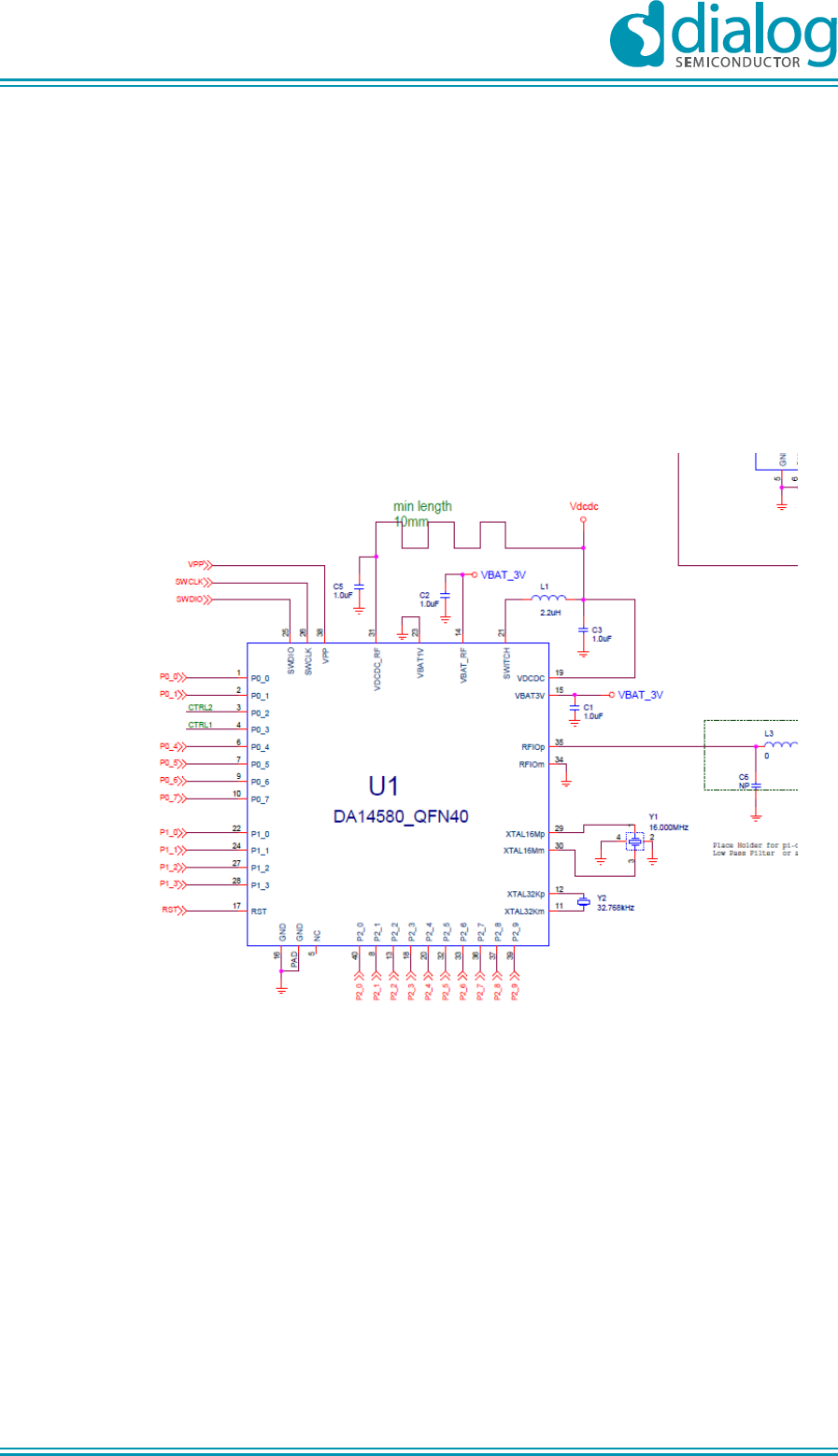
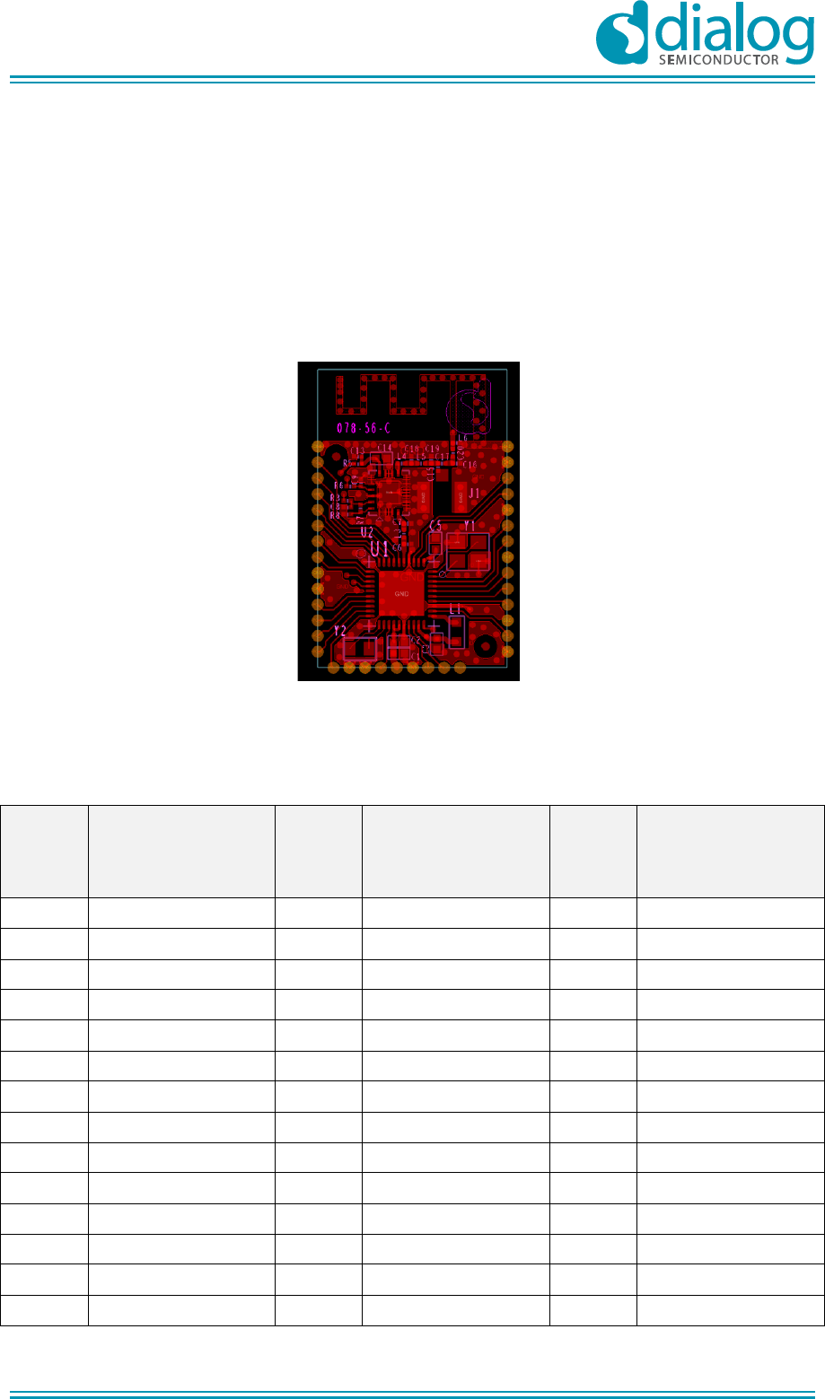
PCBA 4.7
A 2-layer FR4 PCB with 1.024 mm standard thickness is used. The PCB size is 15.25x24 mm. There
are 37 connection pads which are made as castellation (1/2 open drill) with 1.27 mm pitch.
The connection pad assignment is shown in Table 8 below. The pin numbering is counter clockwise,
as seen from the PCB top starting in the top left corner.
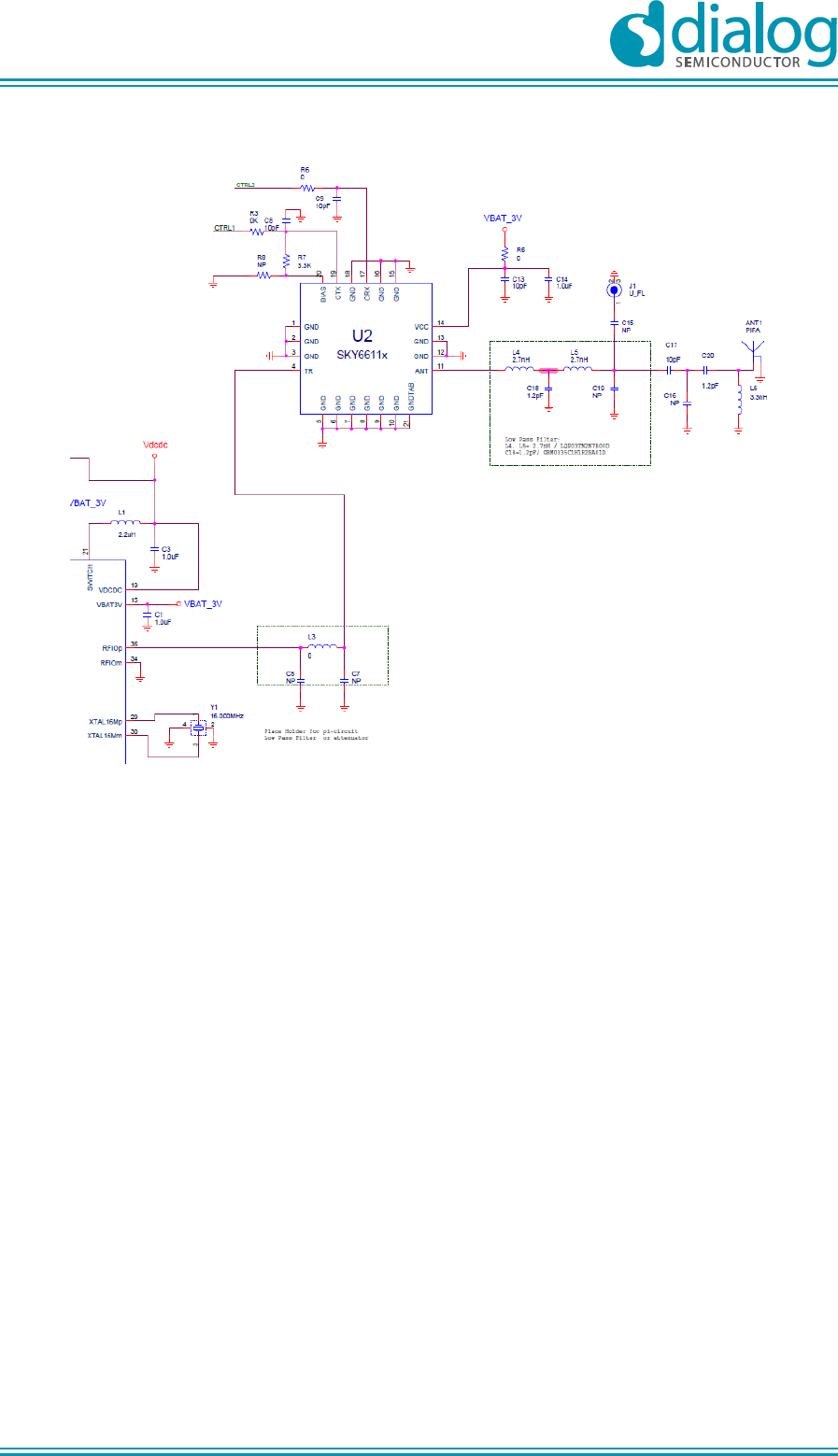
Schematic and BOM are presented in Figure 25 and Table 9.
1
2
3
4
5
6
7
8
9
10
11
12
13
14
1
37
36
35
34
33
32
31
30
29
28
27
26
25
24
15 16 17 18 19 20 21 22 23
Figure 24: Top view of PCBA
Table 8: Module Pin assignment
Pin
Signal name
(Left side of the PCB
seen from the top)
Pin
Signal name
(Bottom side of the
PCB seen from the
top)
Pin
Signal name
(Right side of the
PCB seen from the
top)
1
GND
15
P0_7
29
SWCLK
2
P2_7
16
GND
30
GND
3
P2_8
17
GND
31
P1_2
4
VPP
18
P2_2
32
P1_3
5
P2_9
19
VBAT_3V
33
GND
6
P2_0
20
GND
34
P2_5
7
P0_0
21
RST
35
P2_6
8
P0_1
22
P2_3
36
GND
9
GND
23
P2_4
37
GND
10
GND
24
GND
11
P0_4
25
P1_0
12
P0_5
26
GND
13
P2_1
27
P1_1
14
P0_6
28
SWDIO
UM-B-045
DA14580 Range extender v.2 reference application
Company confidential
User manual
Revision 1.1
14-September-2015
CFR0012-00 Rev 1
28 of 60
© 2015 Dialog Semiconductor
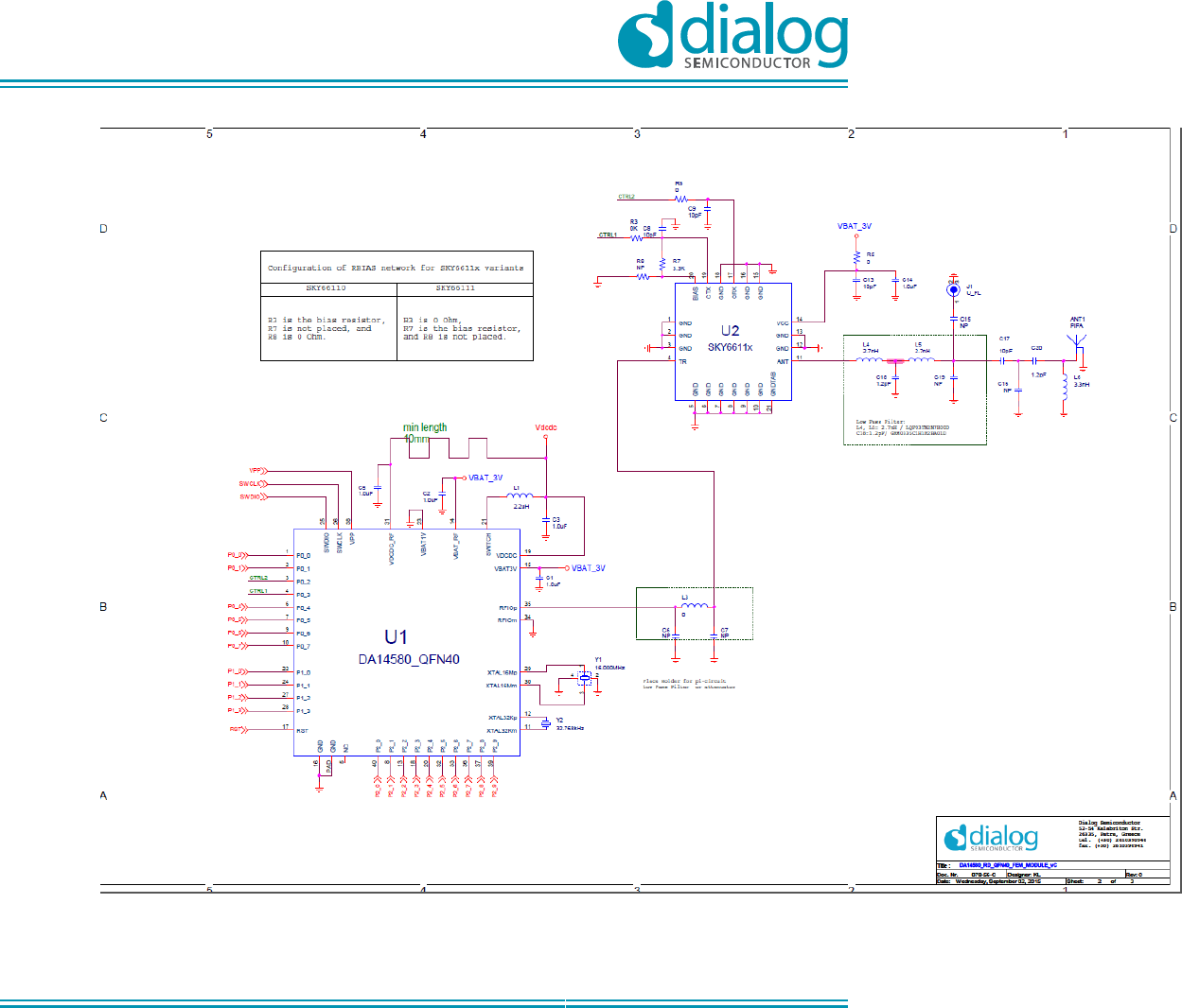
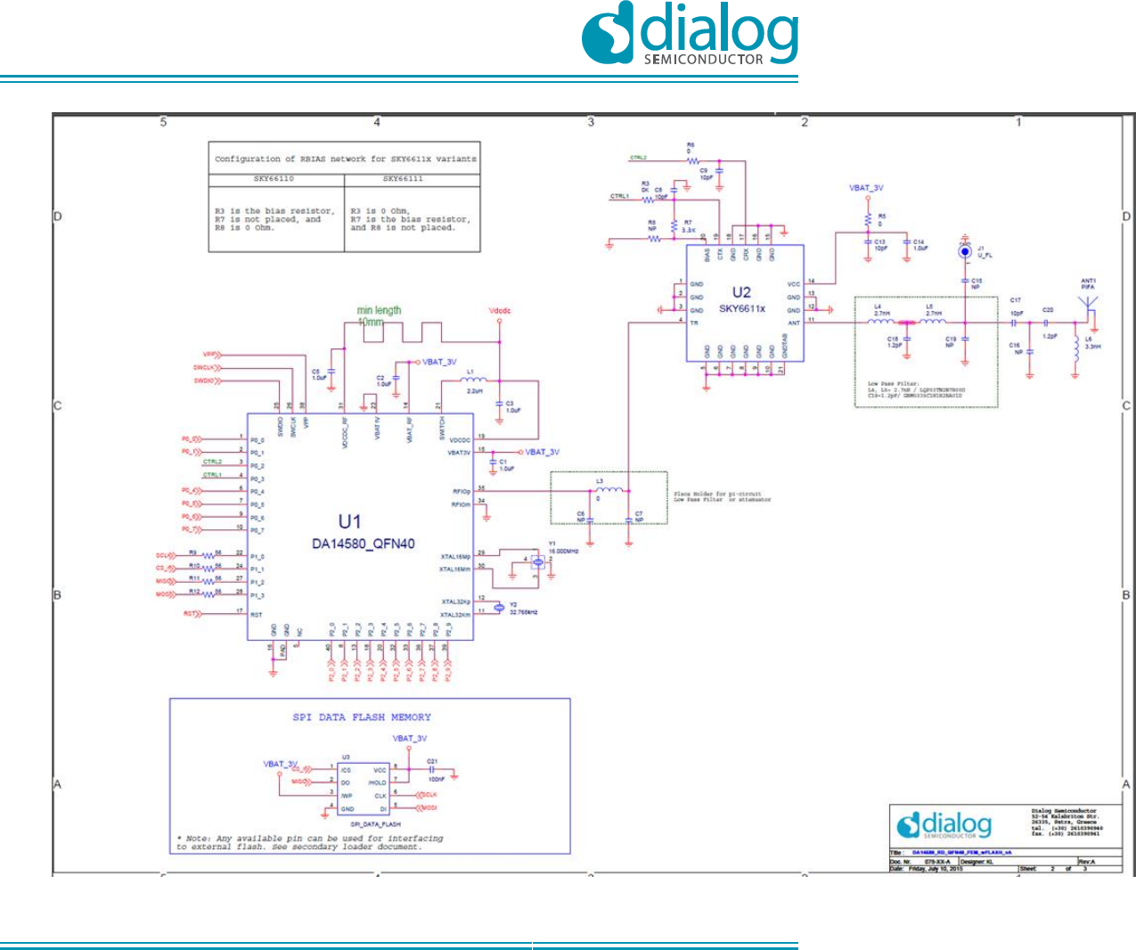
Figure 25: Schematic of DA14580 Range Extender v.2 Module
UM-B-045
DA14580 Range extender v.2 reference application
Company confidential
User manual
Revision 1.1
14-September-2015
CFR0012-00 Rev 1
29 of 60
© 2015 Dialog Semiconductor
Table 9: Bill of Materials
Ref.
Value
Description
Manuf.
MPN
Footpr.
U1
DA1458
0_QFN4
0
BT Low Energy System on a Chip
Dialog
Semiconductor
DA14580-01AT1
QFN40
U2
SKY661
11
Front-End Module, 2.4GHz-
2.485GHz
Skyworks
Solutions, Inc.
SKY66111-11
MCM
L3, R3,
R5, R6
0
RES 0.0 OHM 1/20W 0201 SMD
Vishay/Dale
CRCW02010000Z0ED
0201
R7
3.3K
RES 3.3K OHM 50mW 1% 0201
SMD
Vishay/Dale
CRCW02013K30FKED
0201
Y1
16.000M
Hz
CRYSTAL 16MHZ 10PF SMD
TXC
Corporation
7M-16.000MEEQ-T
Y2
32.768k
Hz
CRYSTAL 32.768KHZ 7PF SMD
Abracon
Corporation
ABS07-32.768KHZ-7-T
C1, C2,
C3, C5,
C14
1.0uF
CAP MLCC 1.0uF 10V X5R 10%
TDK
Corporation
C1005X5R1A105K050BB
0402
C8, C9,
C13, C17
10pF
CAP MLCC 0201 10pF 25volts
C0G
Murata
GRM0335C1E100JA01D
0201
C18, C20
1.2pF
CAP MLCC 0201 1.2pF 25volts
C0G +/-0.25pF
Murata
GRM0335C1E1R2CA01D
0201
L1
2.2uH
INDUCTOR Power 2.2uH,
500mA, 400MHz
Taiyo Yuden
BRL1608T2R2M
0603
L4,L5
2.7nH
Fixed Inductors 2.7 NH +-.1NH
Murata
LQP03TN2N7B00D
0201
L6
3.3nH
Fixed Inductors 3.3nH 0.1nH
500MHz
Murata
LQP03TN3N3B02D
0201
J1
NP
RF Connectors / Coaxial
Connectors UMC STRT JACK
RECEP SURFACE MOUNT
Johnson / Cinch
Connectivity
Solutions
128-0711-201
UMC
Not Populated Components
Ref.
Value
Description
Manuf.
MPN
Footpr.
C6,C7,C
15,C16,C
19
NP
Capacitors
R8
NP
Resistors
ANT1
Printed Antenna
TP1,TP2
Test Points
UM-B-045
DA14580 Range extender v.2 reference application
Company confidential
User manual
Revision 1.1
14-September-2015
CFR0012-00 Rev 1
30 of 60
© 2015 Dialog Semiconductor
Development Mode-Peripheral Pin Mapping 4.8
On the following table the pins used for development/ testing are described.
Table 10: Development/ testing mode pin mapping
SoC
Pin #
DA14580
assigned
Pins
Function
SoC
Pin #
DA14580
assigned
Pins
Function
1
P0_0
Available External Use
21
SWITCH
Connection for the external
DCDC-converter inductor.
2
P0_1
Available External Use
22
P1_0
Available External Use
3
P0_2
PA_Rx Enable
23
VBAT1V
4
P0_3
PA_Tx Enable
24
P1_1
Available External Use
5
NC
25
P1_5
SWDIO
6
P0_4
UART TX
26
P1_4
SWCLK
7
P0_5
UART RX
27
P1_2
Available External Use
8
P2_1
Available External Use
28
P1_3
Available External Use
9
P0_6
Available External Use
29
XTAL16Mp
10
P0_7
WLAN coexist
30
XTAL16Mm
11
XTAL32Km
31
VDCDC_RF
12
XTAL32Kp
32
P2_5
Available External Use
13
P2_2
Available External Use
33
P2_6
Available External Use
14
VBAT_RF
34
RFIOm
15
VBAT3V
35
RFIOp
16
GND
36
P2_7
Available External Use
17
RST
RESET
37
P2_8
Available External Use
18
P2_3
Available External Use
38
VPP
19
VDCDC
39
P2_9
Available External Use
20
P2_4
Available External Use
40
P2_0
Available External Use
*Note: Any available pin can be used for interfacing external SPI data Flash. See secondary boot loader
document for further details4
UM-B-045
DA14580 Range extender v.2 reference application
Company confidential
User manual
Revision 1.1
14-September-2015
CFR0012-00 Rev 1
31 of 60
© 2015 Dialog Semiconductor
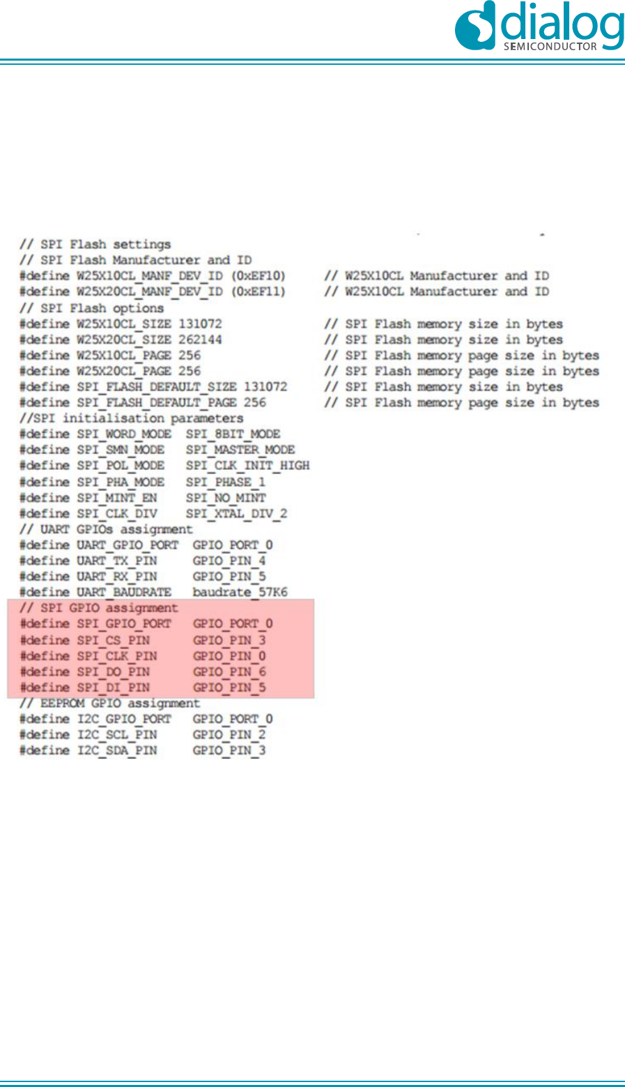
By default in the secondary boot loader4 all the SPI GPIO signals are assigned to Port0. However as
it has been mentioned in paragraph 4.4.1, P0_2 and P0_3 pins are utilized to extract the radio control
signals. So if SPI communication with a peripheral is needed, a modification in the configuration
settings for the peripherals contained in header file periph_setup.h can be made.
Figure 26: DA14580/581/583 configuration settings for peripherals, periph_setup.h
UM-B-045
DA14580 Range extender v.2 reference application
Company confidential
User manual
Revision 1.1
14-September-2015
CFR0012-00 Rev 1
32 of 60
© 2015 Dialog Semiconductor
Software 4.9
The following instructions are based DA14580_581_583_SDK_3.0.10.1. Instructions are valid for
both Keil 4 and Keil 5 projects. Screenshots shown are in Keil 5.
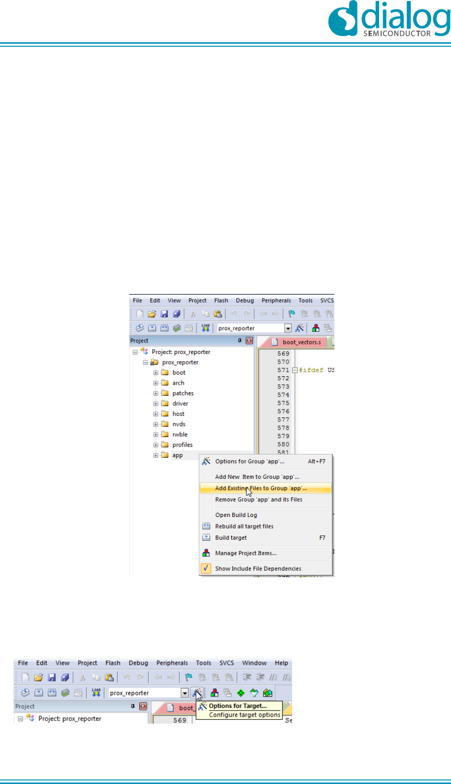
Inserting in a project (example in proximity reporter)
1. Copy app_range_extender folder to dk_apps\src\modules\app\src\app_utils
2. Open the project and add app_range_extender.c in app group of the keil project
Right click ‘apps’ and select “Add existing files to Group ‘app’ ”. Add
app_range_extender.c
Figure 27: Step 2 of adding app_range_extender
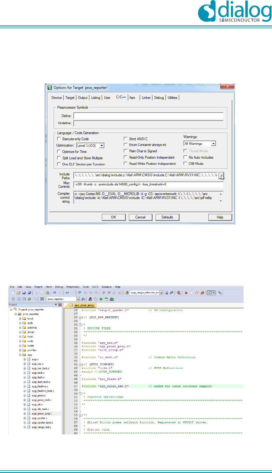
3. Add the app_range_extender folder in the compiler include paths.
Figure 28: Step 3a of adding app_range_extender
UM-B-045
DA14580 Range extender v.2 reference application
Company confidential
User manual
Revision 1.1
14-September-2015
CFR0012-00 Rev 1
33 of 60
© 2015 Dialog Semiconductor
In the target options, select the C/C++ tab and in the end add:
.\..\..\..\..\ src\modules\app\src\app_utils\app_range_extender
(separate from the previous path with a semicolon)
Figure 29: Step 3b of adding app_range_extender
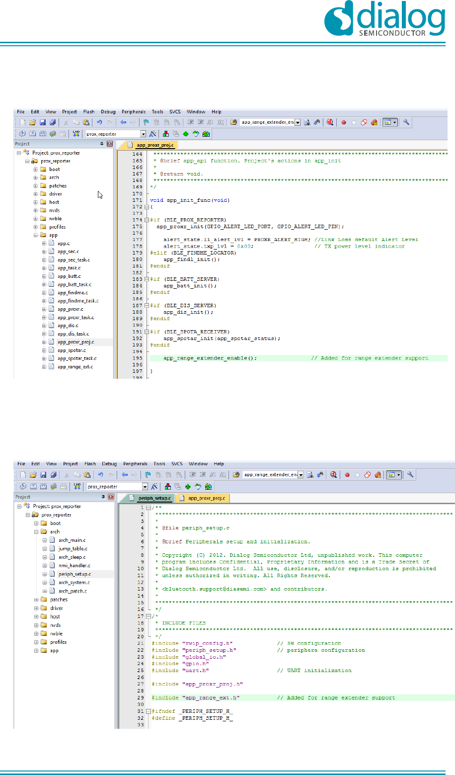
4. In app_<project>_proj file, add the line:
#include "app_range_ext.h" in the Include files section
Figure 30: Step 4a of adding app_range_extender
UM-B-045
DA14580 Range extender v.2 reference application
Company confidential
User manual
Revision 1.1
14-September-2015
CFR0012-00 Rev 1
34 of 60
© 2015 Dialog Semiconductor
and call app_range_extender_enable() in app_init_func()
Figure 31: Step 4b of adding app_range_extender
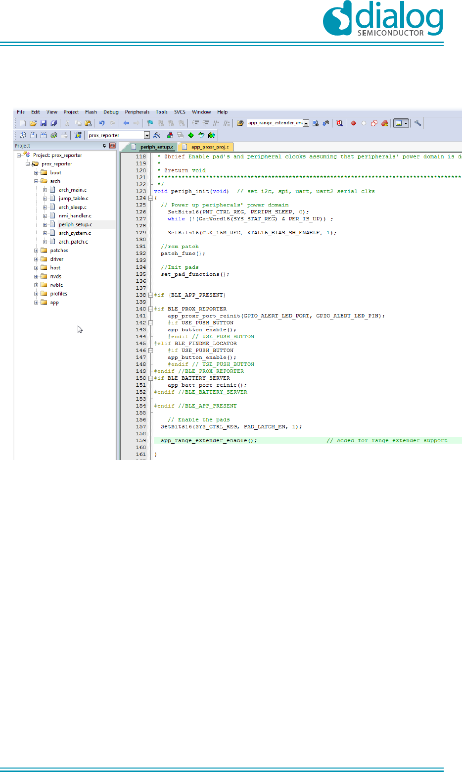
5. In periph_setup.c, add the line:
#include "app_range_ext.h" in the Include files section
Figure 32: Step 5a of adding app_range_extender
UM-B-045
DA14580 Range extender v.2 reference application
Company confidential
User manual
Revision 1.1
14-September-2015
CFR0012-00 Rev 1
35 of 60
© 2015 Dialog Semiconductor
and call app_range_extender_enable()at the end of periph_init()
Figure 33: Step 5b of adding app_range_extender
UM-B-045
DA14580 Range extender v.2 reference application
Company confidential
User manual
Revision 1.1
14-September-2015
CFR0012-00 Rev 1
36 of 60
© 2015 Dialog Semiconductor
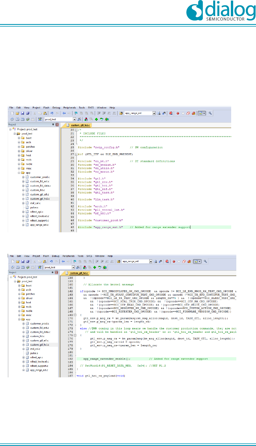
Inserting in the production test tool
1. Follow above steps 1-3
2. In custom_gtl_hci.c, add the line:
#include "app_range_ext.h" in the Include files section
and call app_range_extender_enable()in gtl_hci_rx_header_func()
Figure 34: Inserting app_range_extender in the production test tool

UM-B-045
DA14580 Range extender v.2 reference application
Company confidential
User manual
Revision 1.1
14-September-2015
CFR0012-00 Rev 1
37 of 60
© 2015 Dialog Semiconductor
5 Measurements
Basic performance measurements 5.1
Receiver sensitivity (conducted) 5.1.1
5.1.1.1 Test description
In this test the Rx sensitivity of Range Extender v.2 Module was measured.
5.1.1.2 Test setup
The Range Extender v.2 Module was mounted on a DK Development Board with the use of an
intermediate interposer board. The R&S®CBT Bluetooth® Tester from Rohde & Schwarz was used.
An RF cable assembly was connected to J1 connector (UMC RF Series) and at the other end
through an attenuator to the R&S®CBT Bluetooth® Tester from Rohde & Schwarz. The results from
a dirty transmitter on one of the boards are reported below.
5.1.1.3 Test results
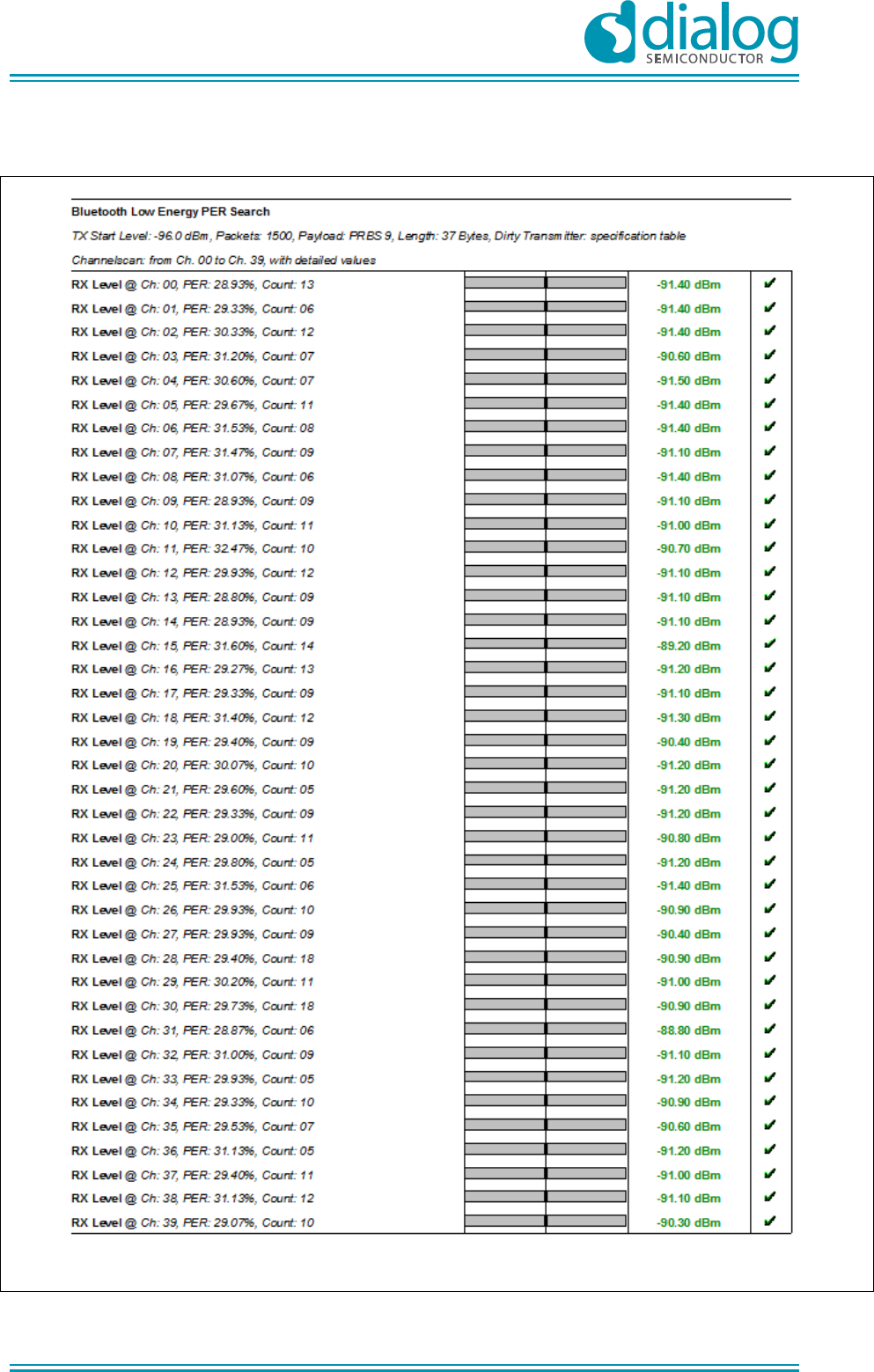
The conducted RF sensitivity with dirty transmitter shows that the sensitivity is better than -90 dBm
for the most of the channels.
UM-B-045
DA14580 Range extender v.2 reference application
Company confidential
User manual
Revision 1.1
14-September-2015
CFR0012-00 Rev 1
38 of 60
© 2015 Dialog Semiconductor
Table 11: Conducted Rx sensitivity
UM-B-045
DA14580 Range extender v.2 reference application
Company confidential
User manual
Revision 1.1
14-September-2015
CFR0012-00 Rev 1
39 of 60
© 2015 Dialog Semiconductor
Transmitter output power (conducted) 5.1.2
5.1.2.1 Test description
In this test the conducted RF output power of Range Extender v.2 Module was measured.
5.1.2.2 Test setup
The Range Extender v.2 Module was mounted on a DK Development Board with the use of an
intermediate interposer board. In order to evaluate the TX output power, production test firmware
was used. Conducted transmitted output power was measured by using the R&S®CBT Bluetooth®
Tester from Rohde & Schwarz. An RF cable assembly was connected to J1 connector (UMC RF
Series) and at the other end through an attenuator to the R&S®CBT Bluetooth® Tester. Bursts of 10
packets were transmitted by the DA14580. The packet length was 37 and the pattern was
“01010101”. Three channels were recorded, channels 0, 19 and 39.
5.1.2.3 Test results
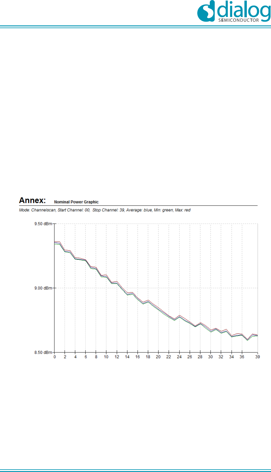
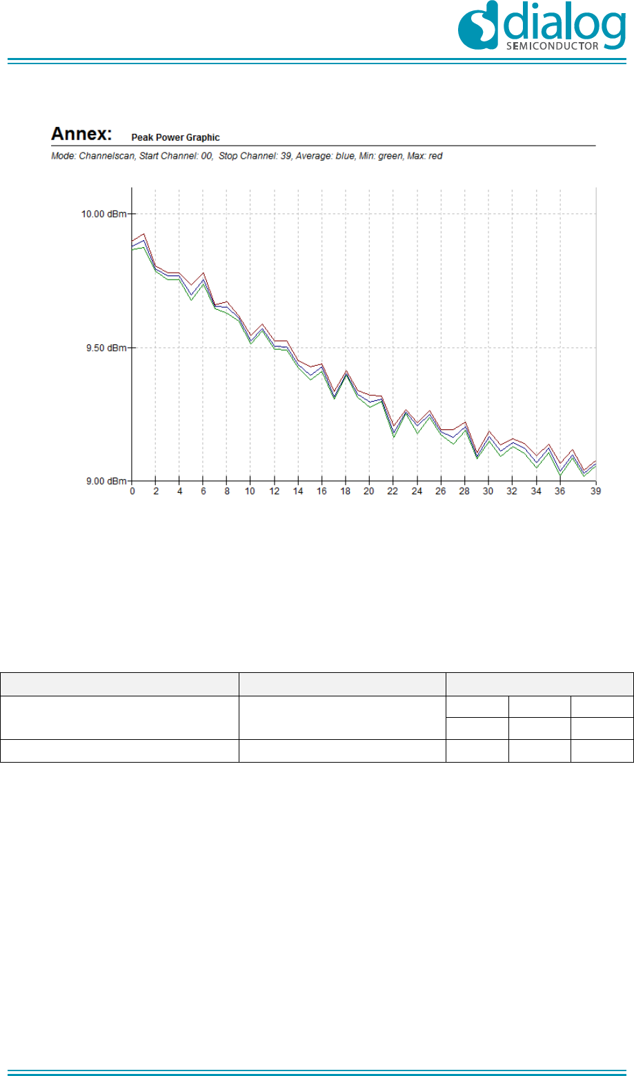
Measurements were performed on a number of samples.
Red: maximum
Blue: average
Green: minimum
Figure 35: Nominal conducted output power per channel
UM-B-045
DA14580 Range extender v.2 reference application
Company confidential
User manual
Revision 1.1
14-September-2015
CFR0012-00 Rev 1
40 of 60
© 2015 Dialog Semiconductor
Red: maximum
Blue: average
Green: minimum
Figure 36: Peak conducted output power per channel
Table 12: Tx output power
Parameter
VBAT_3V (V)
POUT (dBm)
Nominal Tx output power, average
+3.0
CH00
CH19
CH39
9.35
8.87
8.57
Peak Tx output power, average
+3.0
9.88
9.34
9.03
UM-B-045
DA14580 Range extender v.2 reference application
Company confidential
User manual
Revision 1.1
14-September-2015
CFR0012-00 Rev 1
41 of 60
© 2015 Dialog Semiconductor
Current consumption 5.1.3
5.1.3.1 Test setup
The board used in the test presented optimal RF performance. The integrated printed antenna was
used to perform the measurements.
Following instruments were used for the test:
● Multimeter
● 3 V, 100 mA power source
● Agilent N6705B
The current profiles were evaluated using proximity reporter firmware with embedded PA control.
During this test the Advertisement, Connection and Extended Sleep modes were evaluated.
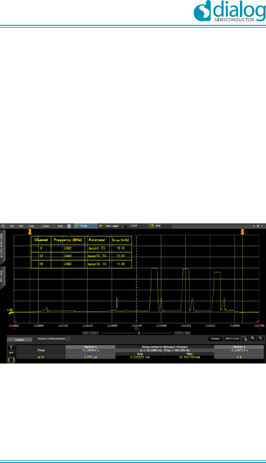
5.1.3.2 Advertisement mode
For this measurement the DUT was supplied by 3 V. FW was downloaded and the JTAG
programmer and then it was disconnected.
Table 13: Peak current during Advertisement mode
Channel
Frequency (MHz)
Parameter
IPEAK (mA)
0
2402
Ipeak0, TX
16.15
12
2440
Ipeak12, TX
15.91
39
2480
Ipeak39, TX
14.68
Figure 37: Supplu current during an Advertisement frame
UM-B-045
DA14580 Range extender v.2 reference application
Company confidential
User manual
Revision 1.1
14-September-2015
CFR0012-00 Rev 1
42 of 60
© 2015 Dialog Semiconductor
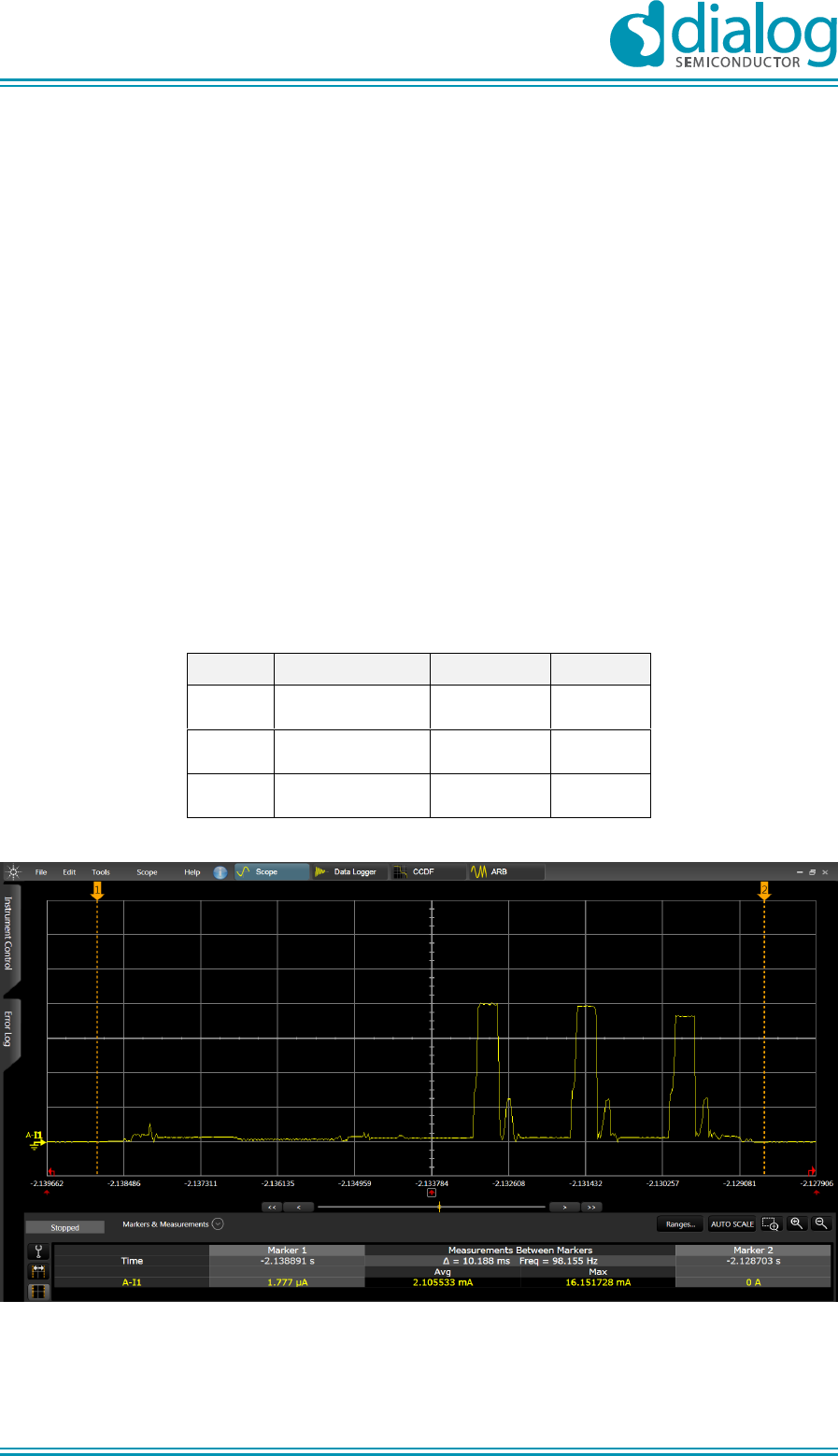
5.1.3.3 Connection mode
For this measurement the DUT was supplied by 3 V. FW was downloaded and the JTAG
programmer was disconnected and connection with an iPhone 4S was established.
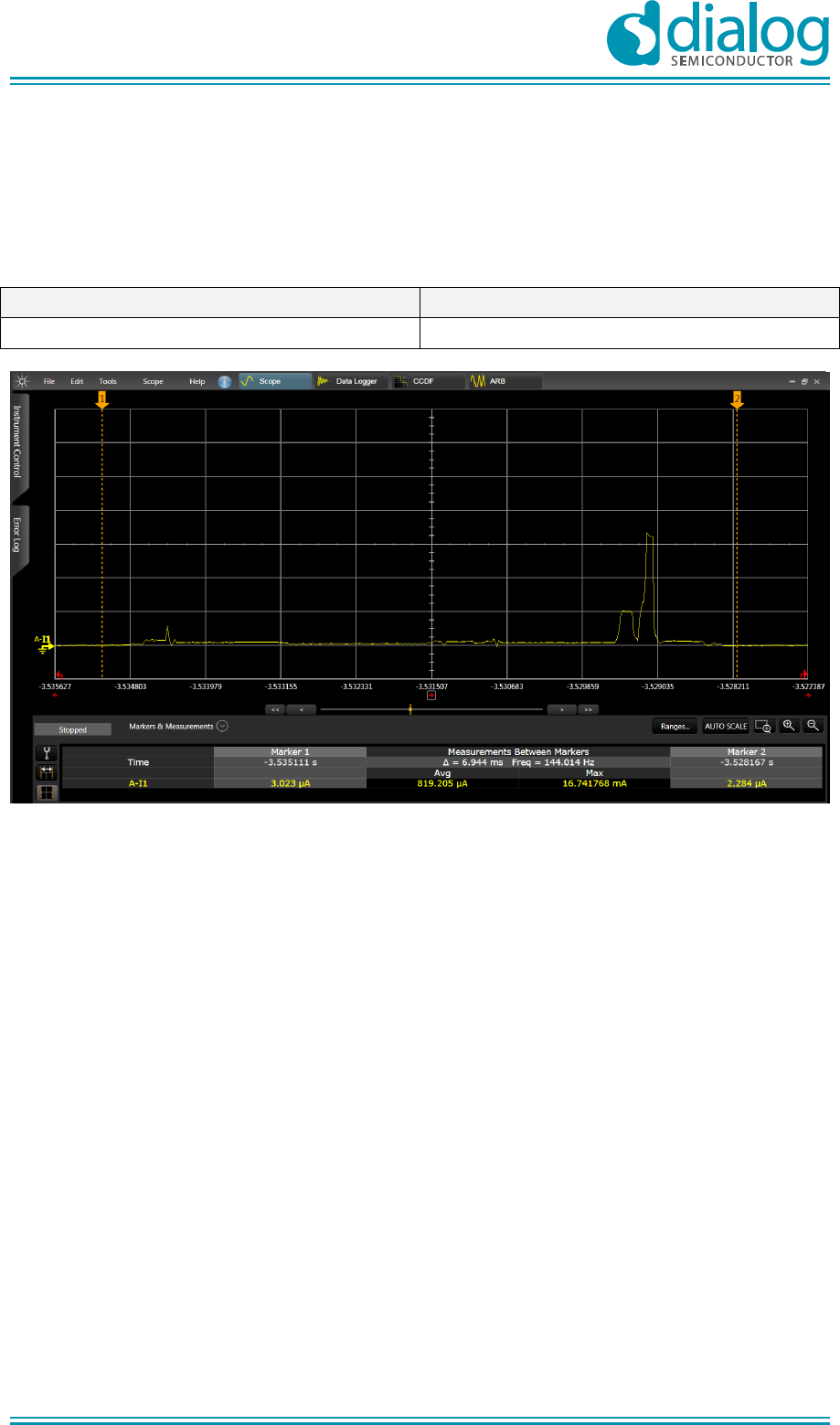
Table 14: Peak current during Connection mode
Parameter
IPEAK (mA)
Ipeak, TX
16.74
Figure 38: Supply current during a Connection frame
UM-B-045
DA14580 Range extender v.2 reference application
Company confidential
User manual
Revision 1.1
14-September-2015
CFR0012-00 Rev 1
43 of 60
© 2015 Dialog Semiconductor
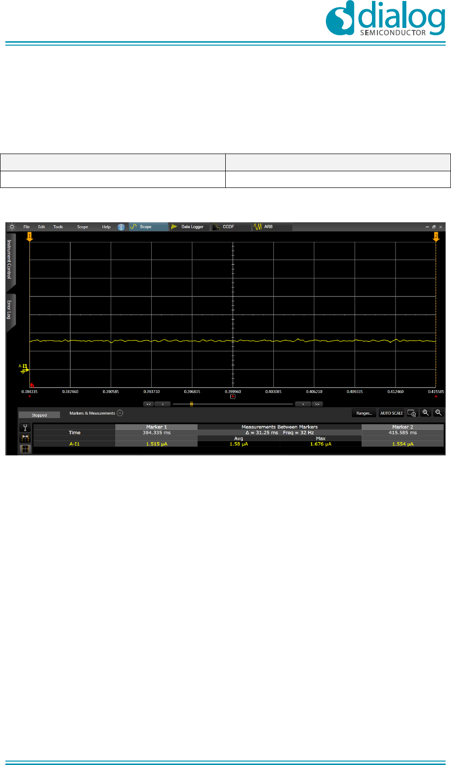
5.1.3.4 Extended sleep mode
For this measurement the DUT was supplied by 3 V. FW was downloaded and the JTAG
programmer was disconnected. FW was setting the RF path to Rx.
Table 15: Average current in Extended Sleep mode
Parameter
IAV (A)
Imean
1.58
Figure 39: Supply current during Extended Sleep mode
UM-B-045
DA14580 Range extender v.2 reference application
Company confidential
User manual
Revision 1.1
14-September-2015
CFR0012-00 Rev 1
44 of 60
© 2015 Dialog Semiconductor
FCC/ ETSI Measurements 5.3
Emission limitation conducted (transmitter) 5.3.1
5.3.1.1 Test description
In this test the level of the harmonics produced by the Tx path was measured.
5.3.1.2 Test setup
The Range Extender v.2 Module was mounted on a DK Development Board with the use of an
intermediate interposer board. In order to evaluate the harmonics levels production, the production
test firmware with embedded PA signal control was used. The boards under test, were set into
continuous transmit mode. An RF cable assembly was connected to J1 connector (UMC RF Series)
and in the other end were connected to the spectrum analyser. Three channels were tested,
channels 0, 19 and 39.
5.3.1.3 Test results
Table 16: Conducted Tx harmonics at VBAT_3V = 3.0 V @ CH00, CH19, CH39
Parameter (dBm)
CH00 – 2402MHz
CH19 – 2440MHz
CH39 – 2480 MHz
2nd harmonic power
-52.40
-52.56
-52.40
3rd harmonic power
-58.54
-58.04
-56.76
4th harmonic power
-55.70
-55.64
-56.81
5th harmonic power
-59.52
-58.06
-56.66
All measurements comply with the limits specified in FCC 15.247/ Sub clause (d). Please note that
the 2nd harmonic power is has a 11.2 dBm margin to the FCC limits (-41.2 dBm).
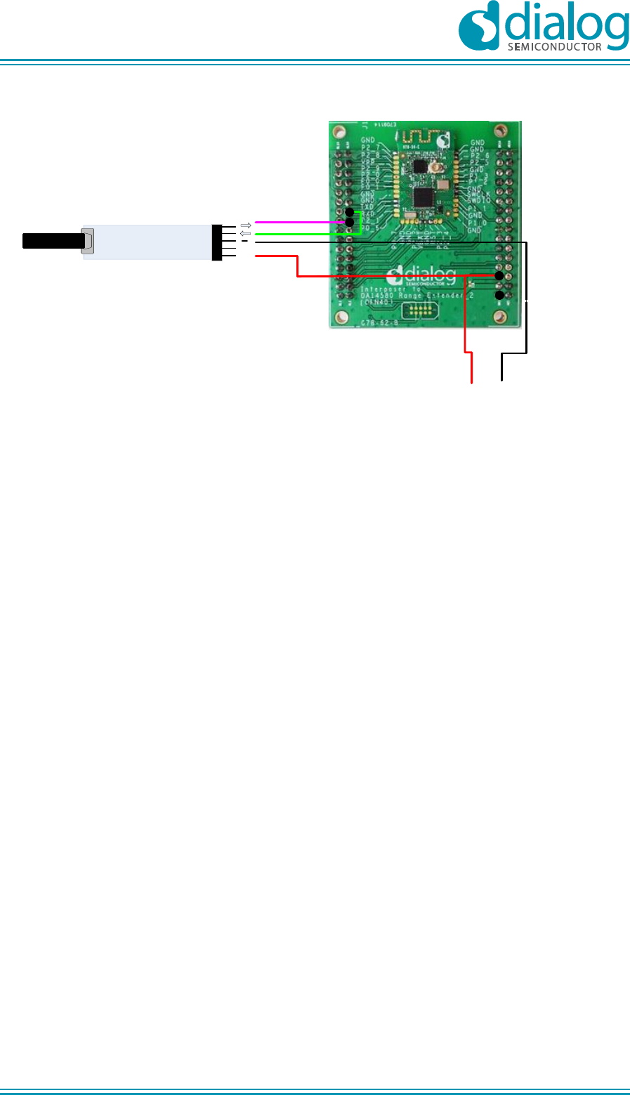
Emission limitation radiated (transmitter) 5.3.2
5.3.2.1 Test description
In this test the level of radiated spurious emissions produced in the Tx mode was measured in the
certified semi-anechoic RF chamber at AT4W labs.
5.3.2.2 Test setup
For the measurements, the device under test comes with its OTP preloaded with the production test
firmware with embedded PA signal control. This software can be configured to generate the required
test patterns. The hardware configuration for the test is shown in Figure 40.
UM-B-045
DA14580 Range extender v.2 reference application
Company confidential
User manual
Revision 1.1
14-September-2015
CFR0012-00 Rev 1
45 of 60
© 2015 Dialog Semiconductor
Rx of QFN40 module
GND
VCC(+3V)
Power Supply
Cable
UART
cable
Tx of QFN40 module
V
USB cable to PC
Figure 40: Range Extender v.2 mounted on the interposer board for radiated measurements
The board was set to continuous transmission mode with a 100% duty cycle.
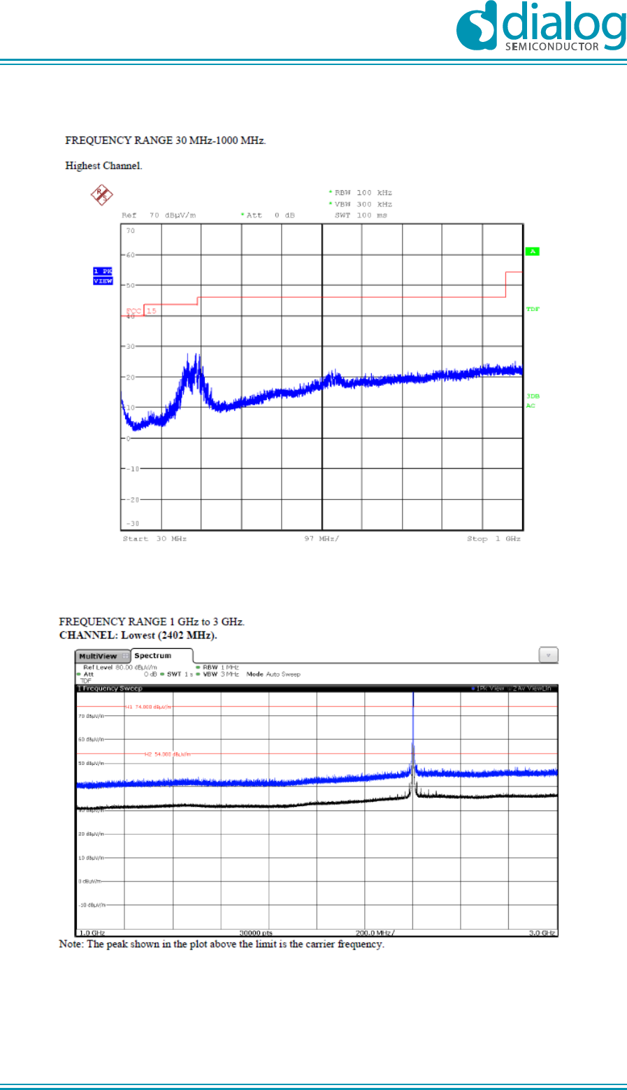
The measurements were conducted for the range of 30 to 1000MHz, 1 GHz to 3 GHz and from 3GHz
to 18 GHz according to FCC Part 15C and for the range of 30 to 1000 MHz and 1 to 12.75 GHz for
ETSI EN 300 328 1.8.1.
A board with Nominal RF Output Power equal to +9.3 dBm was used for this test.
The situation and orientation was varied to find the maximum radiated emission. It was also rotated
360º and the antenna height was varied from 1 to 4 meters to find the maximum radiated emission.
Measurements were made in both horizontal and vertical planes of polarization. All tests were
performed in a semi-anechoic chamber at a distance of 3 m for the frequency range 30 MHz-1000
MHz and at distance of 1m for the frequency ranges above 1 GHz.
5.3.2.3 Test results
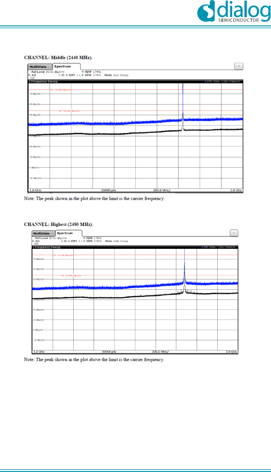
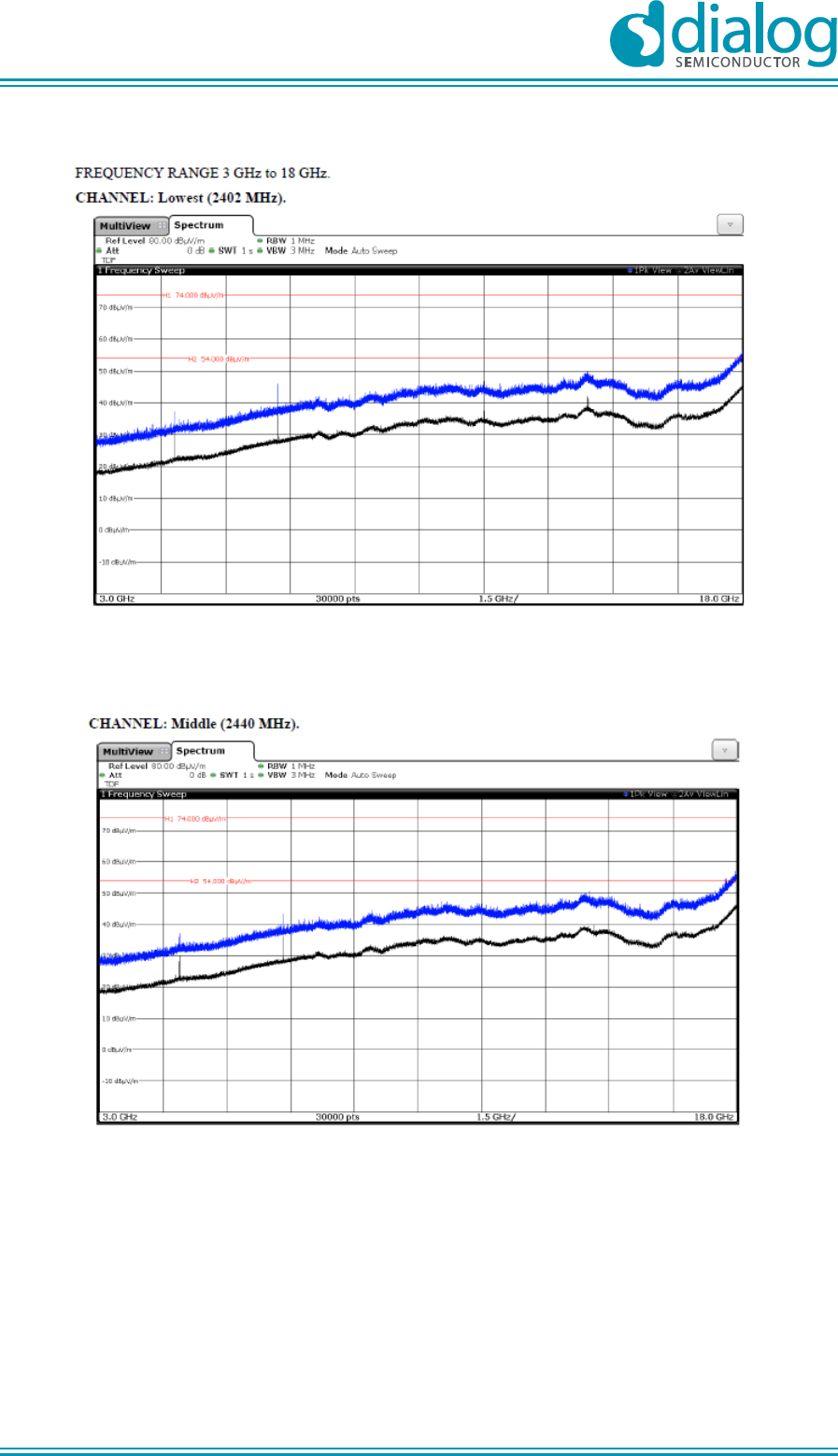
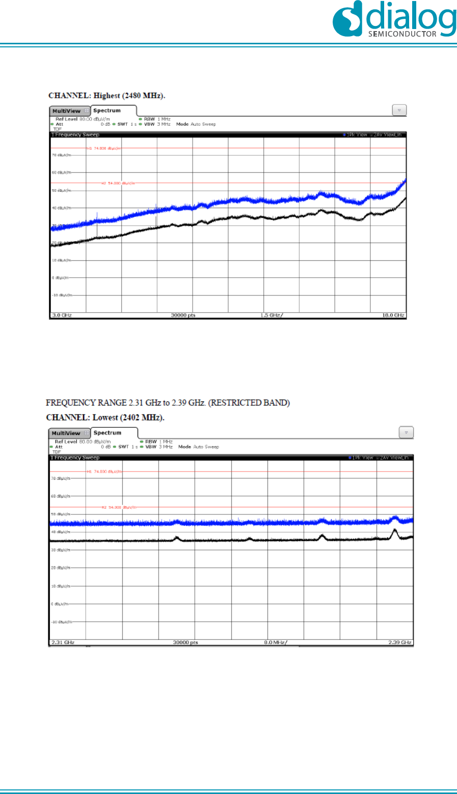
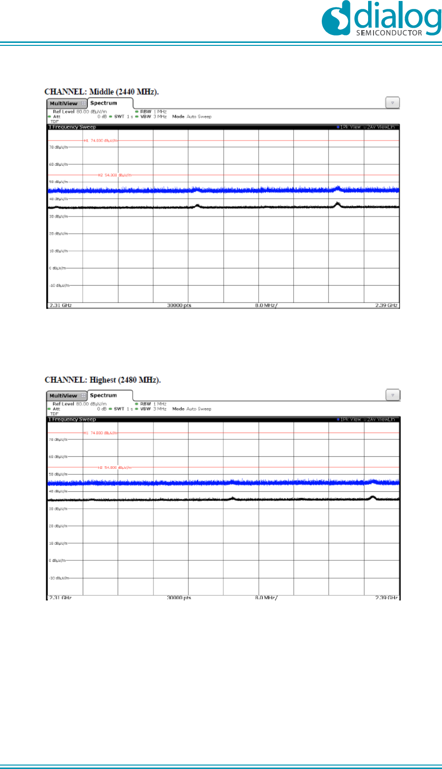
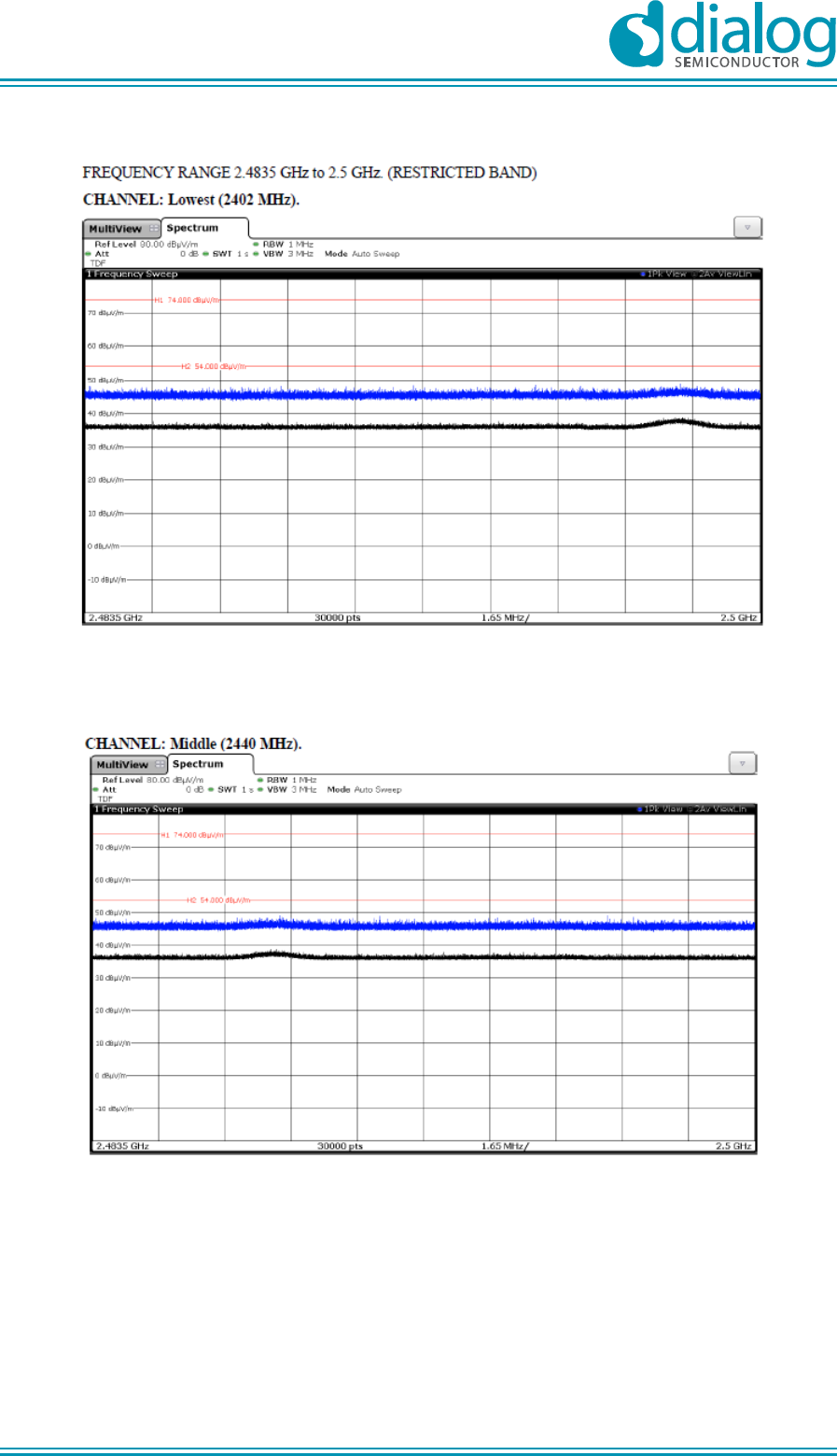
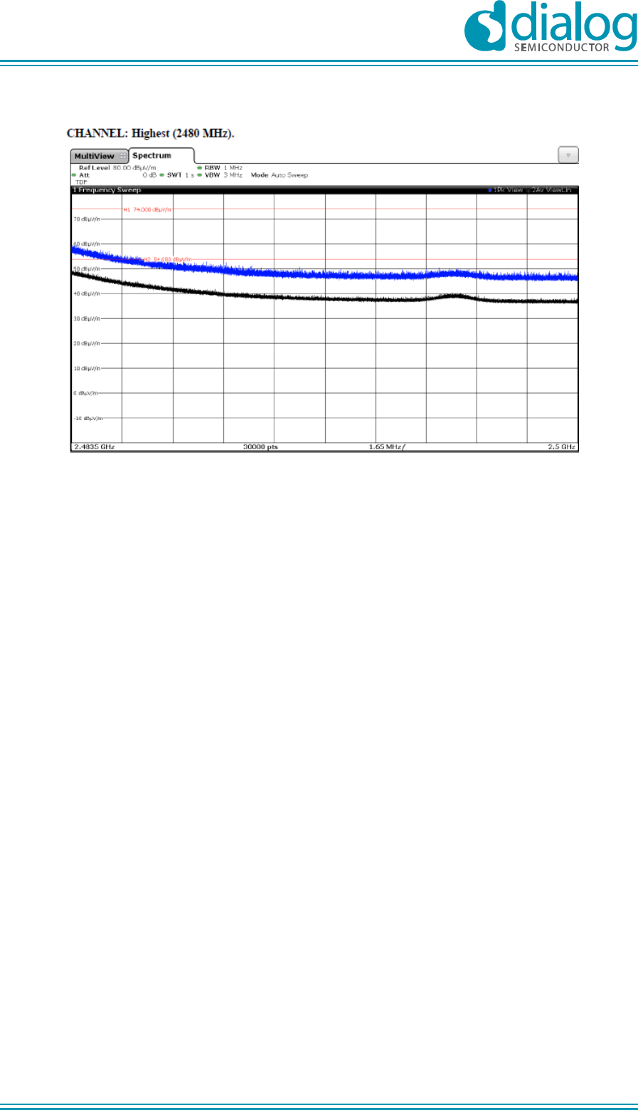
The results of the radiated measurements are given on Figure 41 to Figure 53. All measured FCC
values comply with the emission limits specified in FCC 14.247/ Sub-clause (d). Additionally radiated
emissions limits which fall in restricted bands, as defined in FCC 15.205(a) also comply with the
radiated emissions limits specified in 15.209.
As far as ETSI transmitter unwanted emission in the spurious domain, they all comply to the limits
described in ETSI 300 328 1.8.1 paragraph 4.3.1.9.2.
UM-B-045
DA14580 Range extender v.2 reference application
Company confidential
User manual
Revision 1.1
14-September-2015
CFR0012-00 Rev 1
46 of 60
© 2015 Dialog Semiconductor
Figure 41: FCC, Frequency Range from 30MHz to 1 GHz, CH39
Figure 42: FCC, Frequency from 1GHz to 3GHz, CH00
UM-B-045
DA14580 Range extender v.2 reference application
Company confidential
User manual
Revision 1.1
14-September-2015
CFR0012-00 Rev 1
47 of 60
© 2015 Dialog Semiconductor
Figure 43: FCC, Frequency from 1GHz to 3GHz, CH19
Figure 44: FCC, Frequency from 1GHz to 3GHz, CH39
UM-B-045
DA14580 Range extender v.2 reference application
Company confidential
User manual
Revision 1.1
14-September-2015
CFR0012-00 Rev 1
48 of 60
© 2015 Dialog Semiconductor
Figure 45: FCC, Frequency from 3GHz to 18GHz, CH00
Figure 46: FCC, Frequency from 3GHz to 18GHz, CH19
UM-B-045
DA14580 Range extender v.2 reference application
Company confidential
User manual
Revision 1.1
14-September-2015
CFR0012-00 Rev 1
49 of 60
© 2015 Dialog Semiconductor
Figure 47: FCC, Frequency from 3GHz to 18GHz, CH39
Figure 48: FCC, Frequency Range 2.31 GHz to 2.39 GHz (Restricted band- CH00)
UM-B-045
DA14580 Range extender v.2 reference application
Company confidential
User manual
Revision 1.1
14-September-2015
CFR0012-00 Rev 1
50 of 60
© 2015 Dialog Semiconductor
Figure 49: FCC, Frequency Range 2.31 GHz to 2.39 GHz (Restricted band- CH19)
Figure 50: FCC, Frequency Range 2.31 GHz to 2.39 GHz (Restricted band- CH39)
UM-B-045
DA14580 Range extender v.2 reference application
Company confidential
User manual
Revision 1.1
14-September-2015
CFR0012-00 Rev 1
51 of 60
© 2015 Dialog Semiconductor
Figure 51: FCC, Frequency Range 2.4385 GHz to 2.5 GHz (Restricted band- CH00)
Figure 52: FCC, Frequency Range 2.4385 GHz to 2.5 GHz (Restricted band- CH19)
UM-B-045
DA14580 Range extender v.2 reference application
Company confidential
User manual
Revision 1.1
14-September-2015
CFR0012-00 Rev 1
52 of 60
© 2015 Dialog Semiconductor
Figure 53: FCC, Frequency Range 2.4385 GHz to 2.5 GHz (Restricted band-CH39)

UM-B-045
DA14580 Range extender v.2 reference application
Company confidential
User manual
Revision 1.1
14-September-2015
CFR0012-00 Rev 1
53 of 60
© 2015 Dialog Semiconductor
6 FCC/IC Certification and CE marking
Standards and conformity assessment 6.1
The Range Extender v.2 module was tested and found compliant by a qualified laboratory to the
following standards:
For FCC/IC certification:
● Complete RF testing according to FCC part 15.247, 15.209.
● FCC Rules and Regulations 47 CFR Chapter I Part 15 Subpart B (10-01-12 Edition) and ICES-
003 ISSUE 5. This covers:
o Continuous Conducted Emission of Power Leads, frequency range 0.15 ÷ 30 MHz.
o Radiated Emission – Electromagnetic field, frequency range 30 MHz ÷ 26 GHz
For CE marking:
● Complete RF testing according to ETSI EN 300 328 v1.8.1
● EMC testing according to EN 301 489-1 V.1.9.2 & EN 301 489-17 V2.2.1
o Radiated Emission- Electromagnetic Field measure. Frequency Range 30 MHz ÷ 6 GHz.
Test standard EN 55022 (2010)/ AC (2011).
o Radiated RF Electromagnetic Field Immunity Test. Frequency Range 80 MHz ÷ 2.7 GHz.
Test standard, EN 61000-4-3 (2006) / A1 (2008) / A2 (2010).
● Electrical Safety testing according to EN 61010-1: 2010
o Electrostatic Discharge Immunity Test. Test standard EN 61000-4-2
● RoHS 2011/65/CE (includes screening for 20 elements).
FCC/IC Regulatory notices 6.2
Dialog Semiconductor has not approved any changes or modifications to this device by the user. Any
changes or modifications could void the user’s authority to operate the equipment.
Dialog Semiconductor n’approuve aucune modification apportée à l’appareil par l’utilisateur, quelle
qu’en soit la nature. Tout changement ou modification peuvent annuler le droit d’utilisation de
l’appareil par l’utilisateur.
This device complies with Part 15 of the FCC Rules and Industry Canada licence-exempt RSS
standard(s). Operation is subject to the following two conditions: (1) this device may not cause
interference, and (2) this device must accept any interference, including interference that may cause
undesired operation of the device.
Le présent appareil est conforme aux CNR d'Industrie Canada applicables aux appareils radio
exempts de licence. L'exploitation est autorisée aux deux conditions suivantes : (1) l'appareil ne doit
pas produire de brouillage, et (2) l'utilisateur de l'appareil doit accepter tout brouillage radioélectrique
subi, même si le brouillage est susceptible d'en compromettre le fonctionnement.
This device complies with FCC/IC radiation exposure limits set forth for an uncontrolled environment
and meets the FCC radio frequency (RF) Exposure Guidelines and RSS-102 of the IC radio
frequency (RF) Exposure rules. This transmitter must not be co-located or operating in conjunction
with any other antenna or transmitter.

UM-B-045
DA14580 Range extender v.2 reference application
Company confidential
User manual
Revision 1.1
14-September-2015
CFR0012-00 Rev 1
54 of 60
© 2015 Dialog Semiconductor
Le présent appareil est conforme à l'exposition aux radiations FCC / IC définies pour un
environnement non contrôlé et répond aux directives d'exposition de la fréquence de la FCC
radiofréquence (RF) et RSS-102 de la fréquence radio (RF) IC règles d'exposition. L'émetteur ne doit
pas être colocalisé ni fonctionner conjointement avec à autre antenne ou autre émetteur.
This equipment has been tested and found to comply with the limits for a Class B digital device,
pursuant to part 15 of the FCC Rules. These limits are designed to provide reasonable protection
against harmful interference in a residential installation. This equipment generates uses and can
radiate radio frequency energy and, if not installed and used in accordance with the instructions, may
cause harmful interference to radio communications. However, there is no guarantee that
interference will not occur in a particular installation. If this equipment does cause harmful
interference to radio or television reception, which can be determined by turning the equipment off
and on, the user is encouraged to try to correct the interference by one or more of the following
measures:
- Reorient or relocate the receiving antenna.
- Increase the separation between the equipment and receiver.
- Connect the equipment into an outlet on a circuit different from that to which the receiver is
connected.
- Consult the dealer or an experienced radio/TV technician for help.
CAN ICES-3 (B) / NMB-3 (B)
This Class B digital apparatus complies with Canadian ICES-003.
Cet appareil numérique de classe B est conforme à la norme canadienne NMB-003.
1999/5/EC Directive regulatory notices 6.3
This device has been evaluated against the essential requirements of the 1999/5/EC Directive.
Bulgarian
С настоящето Dialog Semiconductor декларира, че DA14580 RANGE EXTENDER
отговаря на съществените изисквания и другите приложими изисквания на
Директива 1999/5/ЕС.
Croatian
Ovime Dialog Semiconductor ”, izjavljuje da je ovaj DA14580 RANGE EXTENDER je u
skladu s osnovnim zahtjevima i drugim relevantnim odredbama Direktive 1999/5/EC.
Czech
Dialog Semiconductor tímto prohlašuje, že tento DA14580 RANGE EXTENDER je ve
shodě se základními požadavky a dalšími příslušnými ustanoveními směrnice
1999/5/ES.
Danish
Undertegnede Dialog Semiconductor erklærer herved, at følgende udstyr DA14580
RANGE EXTENDER overholder de væsentlige krav og øvrige relevante krav i direktiv
1999/5/EF.
Dutch
Hierbij verklaart Dialog Semiconductor dat het toestel DA14580 RANGE EXTENDER in
overeenstemming is met de essentiële eisen en de andere relevante bepalingen van
richtlijn 1999/5/EG.
English
Hereby, Dialog Semiconductor, declares that this DA14580 RANGE EXTENDER is in
compliance with the essential requirements and other relevant provisions of Directive
1999/5/EC.
UM-B-045
DA14580 Range extender v.2 reference application
Company confidential
User manual
Revision 1.1
14-September-2015
CFR0012-00 Rev 1
55 of 60
© 2015 Dialog Semiconductor
Estonian
Käesolevaga kinnitab Dialog Semiconductor seadme DA14580 RANGE EXTENDER
vastavust direktiivi 1999/5/EÜ põhinõuetele ja nimetatud direktiivist tulenevatele teistele
asjakohastele sätetele.
German
Hiermit erklärt Dialog Semiconductor, dass sich das Gerät DA14580 RANGE
EXTENDER in Übereinstimmung mit den grundlegenden Anforderungen und den
übrigen einschlägigen Bestimmungen der Richtlinie 1999/5/EG befindet.
Greek
ΜΕ ΤΗΝ ΠΑΡΟΥΣΑ Dialog Semiconductor ΔΗΛΩΝΕΙ ΟΤΙ DA14580 RANGE
EXTENDER ΣΥΜΜΟΡΦΩΝΕΤΑΙ ΠΡΟΣ ΤΙΣ ΟΥΣΙΩΔΕΙΣ ΑΠΑΙΤΗΣΕΙΣ ΚΑΙ ΤΙΣ ΛΟΙΠΕΣ
ΣΧΕΤΙΚΕΣ ΔΙΑΤΑΞΕΙΣ ΤΗΣ ΟΔΗΓΙΑΣ 1999/5/ΕΚ.
Hungarian
Alulírott, Dialog Semiconductor nyilatkozom, hogy a DA14580 RANGE EXTENDER
megfelel a vonatkozó alapvetõ követelményeknek és az 1999/5/EC irányelv egyéb
elõírásainak.
Finnish
Dialog Semiconductor vakuuttaa täten että NAME OF PRODUCT tyyppinen laite on
direktiivin 1999/5/EY oleellisten vaatimusten ja sitä koskevien direktiivin muiden ehtojen
mukainen.
French
Par la présente Dialog Semiconductor déclare que l'appareil DA14580 RANGE
EXTENDER est conforme aux exigences essentielles et aux autres dispositions
pertinentes de la directive 1999/5/CE.
Icelandic
Hér með lýsir Dialog Semiconductor yfir því að DA14580 RANGE EXTENDER er í
samræmi við grunnkröfur og aðrar kröfur, sem gerðar eru í tilskipun 1999/5/EC
Italian
Con la presente Dialog Semiconductor dichiara che questo DA14580 RANGE
EXTENDER è conforme ai requisiti essenziali ed alle altre disposizioni pertinenti
stabilite dalla direttiva 1999/5/CE.
Latvian
Ar šo Dialog Semiconductor deklarē, ka DA14580 RANGE EXTENDER atbilst
Direktīvas 1999/5/EK būtiskajām prasībām un citiem ar to saistītajiem noteikumiem.
Lithuanian
Šiuo Dialog Semiconductor deklaruoja, kad šis DA14580 RANGE EXTENDER atitinka
esminius reikalavimus ir kitas 1999/5/EB Direktyvos nuostatas.
Maltese
Hawnhekk, Dialog Semiconductor, jiddikjara li dan DA14580 RANGE EXTENDER
jikkonforma mal-ħtiġijiet essenzjali u ma provvedimenti oħrajn relevanti li hemm fid-
Dirrettiva 1999/5/EC.
Norwegian
Dialog Semiconductor erklærer herved at utstyret DA14580 RANGE EXTENDER er i
samsvar med de grunnleggende krav og øvrige relevante krav i direktiv 1999/5/EF.
Polish
Niniejszym Dialog Semiconductor oświadcza, że DA14580 RANGE EXTENDER jest
zgodny z zasadniczymi wymogami oraz pozostałymi stosownymi postanowieniami
Dyrektywy 1999/5/EC
Portuguese
Dialog Semiconductor declara que este DA14580 RANGE EXTENDER está conforme
com os requisitos essenciais e outras disposições da Directiva 1999/5/CE.
Slovak
Dialog Semiconductor týmto vyhlasuje, že DA14580 RANGE EXTENDER spĺňa
základné požiadavky a všetky príslušné ustanovenia Smernice 1999/5/ES.
Slovenian
Dialog Semiconductor izjavlja, da je ta DA14580 RANGE EXTENDER v skladu z
bistvenimi zahtevami in ostalimi relevantnimi določili direktive 1999/5/ES.
Spanish
Por medio de la presente Dialog Semiconductor declara que DA14580 RANGE
EXTENDER cumple con los requisitos esenciales y cualesquiera otras disposiciones
aplicables o exigibles de la Directiva 1999/5/CE.
Swedish
Härmed intygar Dialog Semiconductor att denna DA14580 RANGE EXTENDER står I
överensstämmelse med de väsentliga egenskapskrav och övriga relevanta
bestämmelser som framgår av direktiv 1999/5/EG.
In order to satisfy the essential requirements of 1999/5/EC Directive, the product is compliant with
the following standards:
UM-B-045
DA14580 Range extender v.2 reference application
Company confidential
User manual
Revision 1.1
14-September-2015
CFR0012-00 Rev 1
56 of 60
© 2015 Dialog Semiconductor
RF spectrum use (R&TTE art.
3.2)
EN 300 328 v1.8.1
EMC (R&TTE art. 3.1b)
EN 301 489-1 V1.9.2 + EN 301 489-17 V2.2.1
Health & Safety (R&TTE art.
3.1a)
EN 60950-1:2006 +A11:2009+ A12:2011 + A1:2010 +
AC:2011 + A2: 2013
The conformity assessment procedure referred to in Article 10 and detailed in Annex IV of Directive
1999/5/EC has been followed with the involvement of the following Notified Body:
AT4 wireless, S.A.
Parque Tecnologico de Andalucía
C/ Severo Ochoa 2
29590 Campanillas – Málaga
SPAIN
Notified Body No: 1909
Thus, the following marking is included in the product:
There is no restriction for the commercialization of this device in all the countries of the European Union.

UM-B-045
DA14580 Range extender v.2 reference application
Company confidential
User manual
Revision 1.1
14-September-2015
CFR0012-00 Rev 1
57 of 60
© 2015 Dialog Semiconductor
7 Appendix A: Range Extender v.2 with SPI Data Flash
Range Extender v.2 can be used with external SPI Data Flash Memory. Any available pins can be
used to interface the external data Flash. The appropriate configuration settings for peripherals must
be set in secondary boot loader as described in paragraph 4.8. The following application example
schematic contains Range Extender v.2 with external SPI Data Flash.
UM-B-045
DA14580 Range extender v.2 reference application
Company confidential
User manual
Revision 1.1
14-September-2015
CFR0012-00 Rev 1
58 of 60
© 2015 Dialog Semiconductor
Figure 54: Range Extender v.2 Module with external SPI Flash
UM-B-045
DA14580 Range extender v.2 reference application
Company confidential
User manual
Revision 1.1
14-September-2015
CFR0012-00 Rev 1
59 of 60
© 2015 Dialog Semiconductor
8 Revision history
Revision
Date
Description
1.0
16-07-2015
Initial version. FCC/ETSI final certification reports pending for
end of September 2015. All measurement regarding compliance
to FCC/ETSI will be updated from the final certification reports.
All FCC/ ETSI tests have been found to pass.
1.1
14-09-2015
Initial version: modification related to reduction of the output
power.
2.0
With final FCC/ETSI
reports
The document will be updated in the following sections.
- Chapter 4.9: Software: upgrade with version SDK 5.02
- Chapter 4.10: Test platform ( future chapter): PRO DK
Interposer Description
- Chapter 5.3: FCC/ETSI Measurements: upgrade with
final results
- Chapter 6: FCC/IC Certification and CE marking
UM-B-045
DA14580 Range extender v.2 reference application
Company confidential
User manual
Revision 1.1
14-September-2015
CFR0012-00 Rev 1
60 of 60
© 2015 Dialog Semiconductor
Status definitions
Status
Definition
DRAFT
The content of this document is under review and subject to formal approval, which may result in
modifications or additions.
APPROVED
or unmarked
The content of this document has been approved for publication.
Disclaimer
Information in this document is believed to be accurate and reliable. However, Dialog Semiconductor does not give any
representations or warranties, expressed or implied, as to the accuracy or completeness of such information. Dialog
Semiconductor furthermore takes no responsibility whatsoever for the content in this document if provided by any information
source outside of Dialog Semiconductor.
Dialog Semiconductor reserves the right to change without notice the information published in this document, including without
limitation the specification and the design of the related semiconductor products, software and applications.
Applications, software, and semiconductor products described in this document are for illustrative purposes only. Dialog
Semiconductor makes no representation or warranty that such applications, software and semiconductor products will be
suitable for the specified use without further testing or modification. Unless otherwise agreed in writing, such testing or
modification is the sole responsibility of the customer and Dialog Semiconductor excludes all liability in this respect.
Customer notes that nothing in this document may be construed as a license for customer to use the Dialog Semiconductor
products, software and applications referred to in this document. Such license must be separately sought by customer with
Dialog Semiconductor.
All use of Dialog Semiconductor products, software and applications referred to in this document are subject to Dialog
Semiconductor’s Standard Terms and Conditions of Sale, unless otherwise stated.
© Dialog Semiconductor. All rights reserved.
RoHS Compliance
Dialog Semiconductor complies with European Directive 2001/95/EC and from 2 January 2013 onwards to European Directive
2011/65/EU concerning Restriction of Hazardous Substances (RoHS/RoHS2).
Dialog Semiconductor’s statement on RoHS can be found on the customer portal https://support.diasemi.com/. RoHS
certificates from our suppliers are available on request.
Contacting Dialog Semiconductor
United Kingdom (Headquarters)
Dialog Semiconductor PLC
Phone: +44 1793 757700
Germany Headquarters
Dialog Semiconductor GmbH
Phone: +49 7021 805-0
The Netherlands
Dialog Semiconductor B.V.
Phone: +31 73 640 8822
North America
Dialog Semiconductor Inc.
Phone: +1 408 845 8500
Japan
Dialog Semiconductor K. K.
Phone: +81 3 5425 4567
Taiwan
Dialog Semiconductor Taiwan
Phone: +886 281 786 222
Singapore
Dialog Semiconductor Singapore
Phone: +65 64 849929
China
Dialog Semiconductor China
Phone: +86 21 5178 2561
Korea
Dialog Semiconductor Korea
Phone: +82 2 3469 8291
Email:
enquiry@diasemi.com
Web site:
www.dialog-semiconductor.com