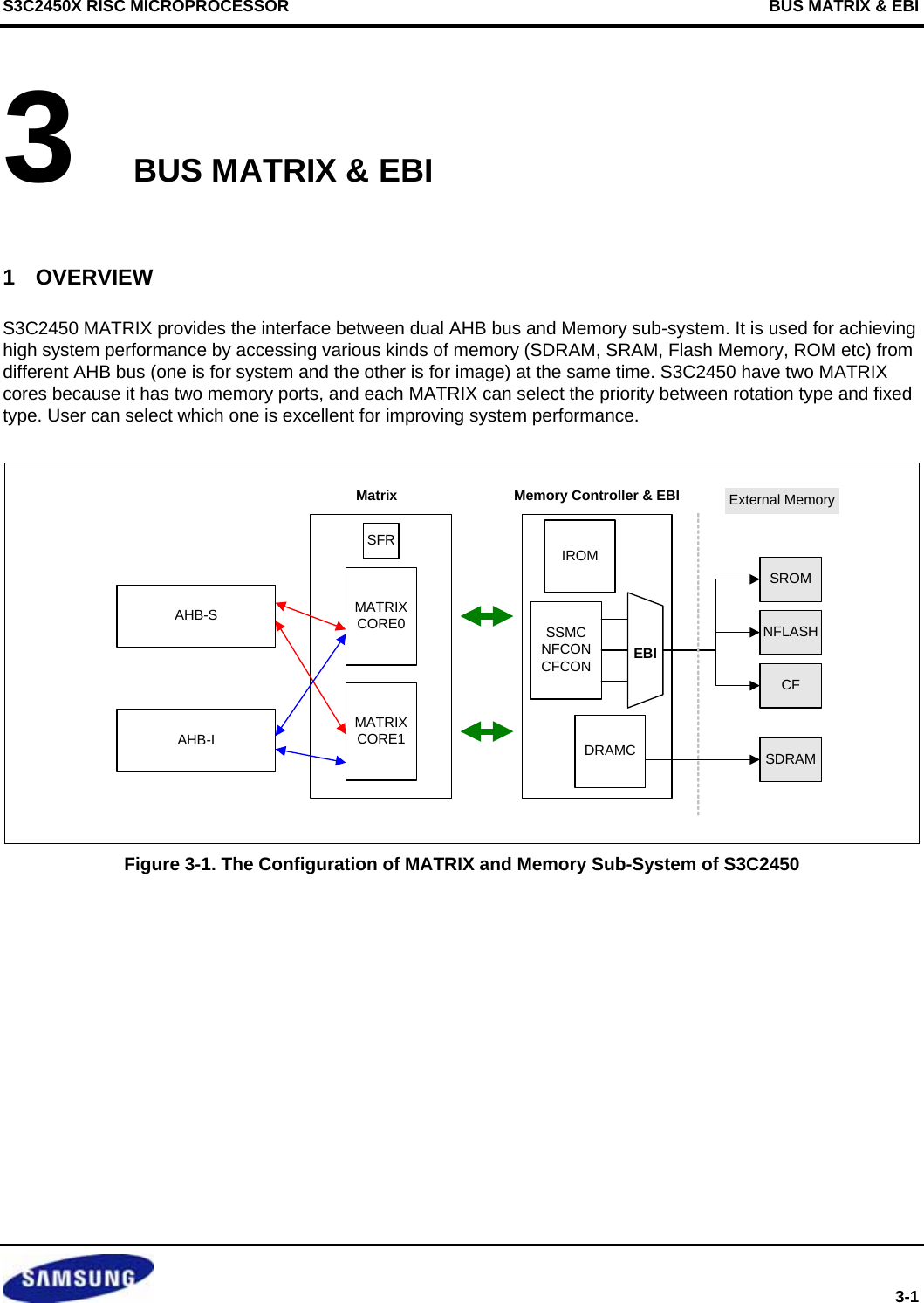
Diasonic Technology Co RVM-704M TOUCH SCREEN MONITOR User Manual KS88C0216
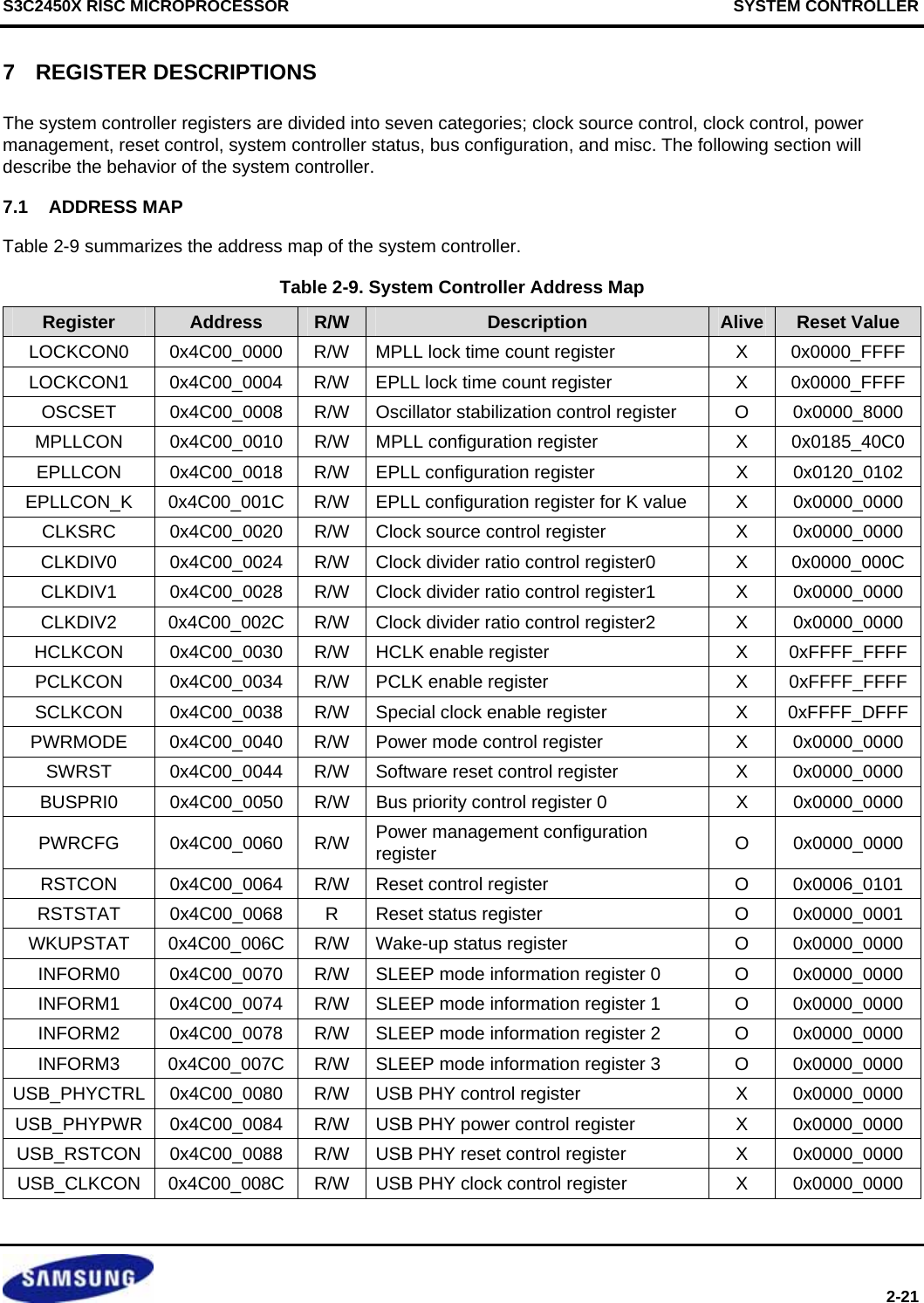
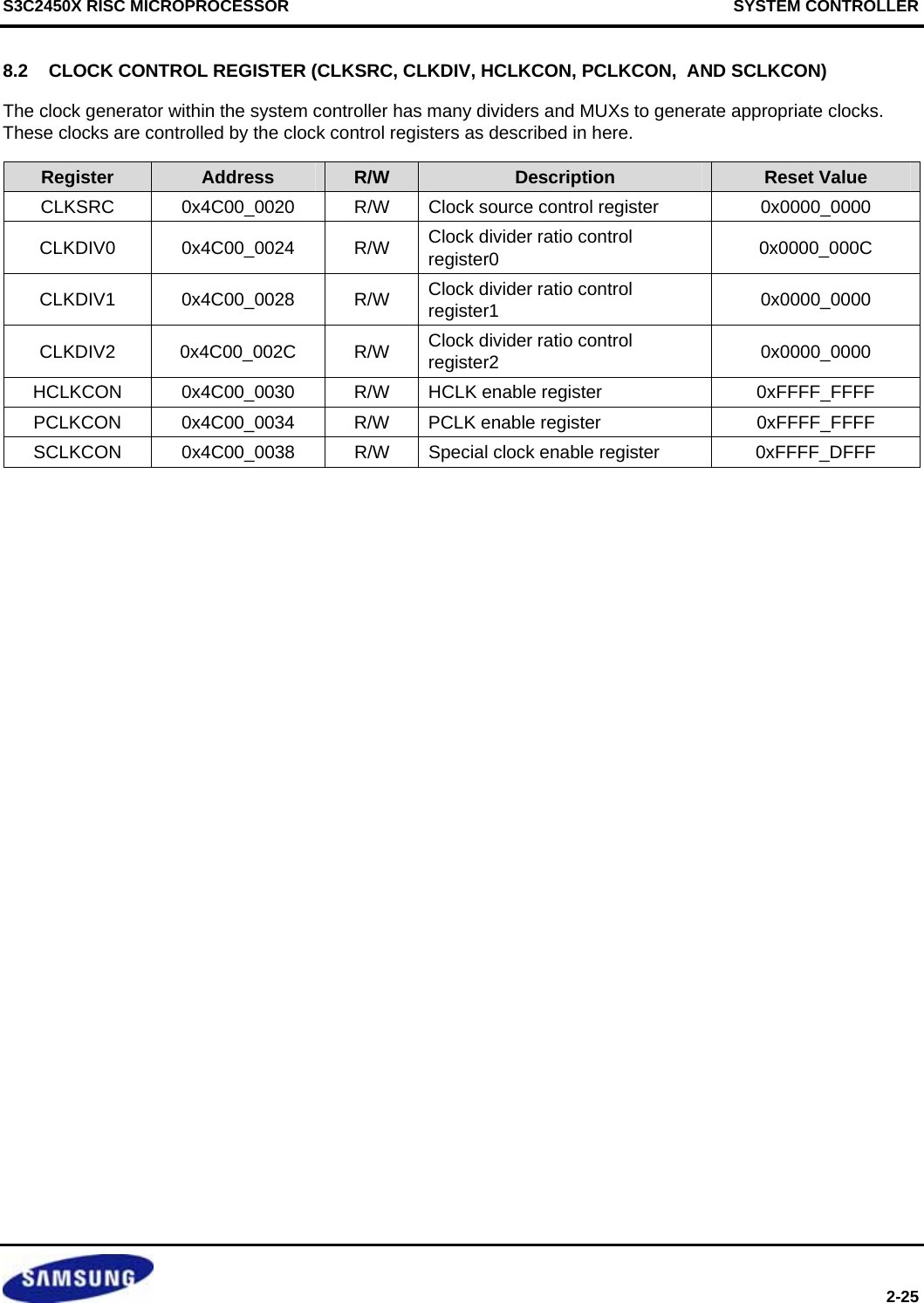
Diasonic Technology Co Ltd TOUCH SCREEN MONITOR KS88C0216
UserManual.wiki
>
Diasonic Technology Co
>
RVM-704M User Manual
>
Users Manual
Contents
1.
User Manual
2.
Users Manual
Users Manual
Navigation menu
Upload a User Manual
Namespaces
Wiki Guide
HTML
PDF
Info
Views
User Manual
Discussion / Help
Navigation
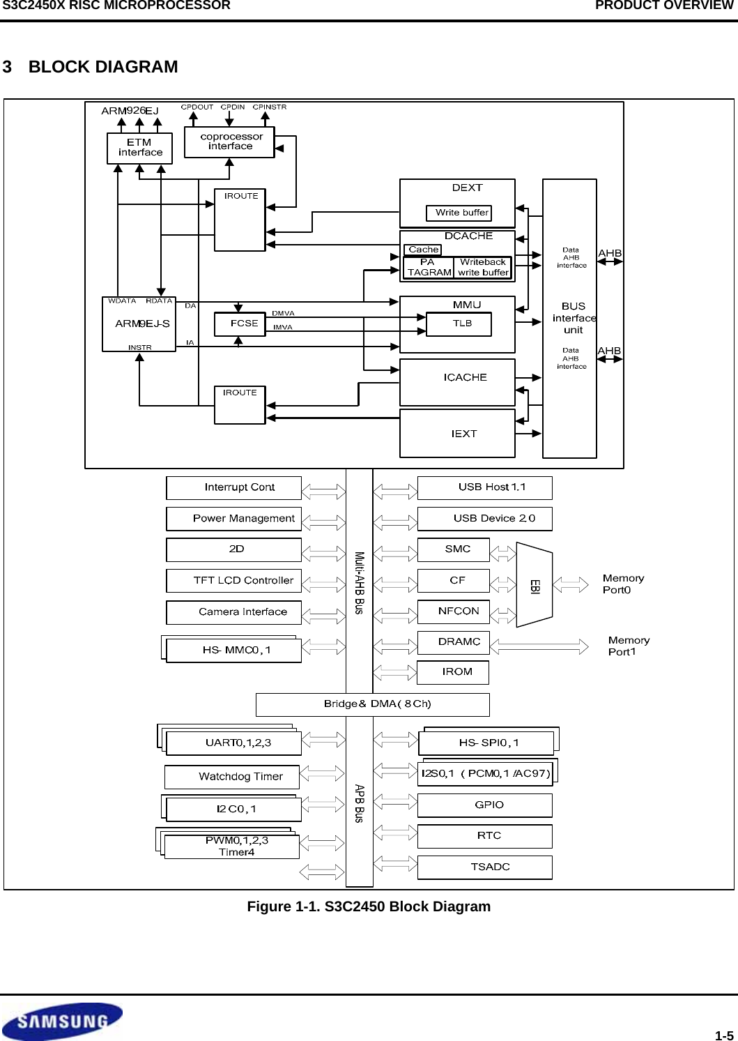
![PRODUCT OVERVIEW S3C2450X RISC MICROPROCESSOR 1-2 2 FEATURES 2.1.1 Architecture • Integrated system for hand-held devices and general embedded applications. • 16/32-Bit RISC architecture and powerful instruction set with ARM926EJ CPU core. • Enhanced ARM architecture MMU to support WinCE, EPOC 32 and Linux. • Instruction cache, data cache, write buffer and Physical address TAG RAM to reduce the effect of main memory bandwidth and latency on performance. • ARM926EJ CPU core supports the ARM debug architecture. • Internal Advanced Microcontroller Bus Architecture (AMBA) (AMBA2.0, AHB/APB). 2.1.2 System Manager • Little/Big Endian support. • Two independent memory bus - one for the ROM/SRAM bus (ROM Bank0~Bank5) and one for the DRAM bus (mSDR/mDDR/DDR2 SDRAM Bank0~Bank1) • Address space: 64M bytes for Rom bank0 ~ bank5, 128M bytes for SDRAM bank0 ~ bank1. • Supports programmable 8/16-bit data bus width for ROM/SRAM bank and programmable 16/32-bit data bus width for SDRAM bank • Fixed bank start address from Rom bank 0 to bank 5 and SDRAM bank 0 to bank1. • Eight memory banks: – Six memory banks for ROM, SRAM, and others (NAND/CF etc.). – Two memory banks for Synchronous DRAM. • Complete Programmable access cycles for all memory banks. • Supports external wait signals to expand the bus cycle. • Supports self-refresh mode in SDRAM for power-down. • Supports various types of ROM for booting (NOR Flash, EEPROM, OneNAND, IROM and others). 2.1.3 NAND Flash • Supports booting from NAND flash memory by selecting OM as IROM boot mode. (Only 8bit Nand and 8ECC is supported when it boots) • 64KB for internal SRAM Buffer(8KB internal buffer for booting) • Supports storage memory for NAND flash memory after booting. • Supports Advanced NAND flash 2.1.4 Cache Memory • 64-way set-associative cache with I-Cache (16KB) and D-Cache (16KB). • 8words length per line with one valid bit and two dirty bits per line. • Pseudo random or round robin replacement algorithm. • Write-through or write-back cache operation to update the main memory. • The write buffer can hold 16 words of data and four addresses. 2.1.5 Clock & Power Manager • On-chip MPLL and EPLL: EPLL generates the clock to operate USB Host, IIS, UART, etc. MPLL generates the clock to operate MCU at maximum 533MHz @ TBD V. • Clock can be fed selectively to each function block by software. • Power mode: Normal, Idle, Stop, Deep Stop and Sleep mode Normal mode: Normal operating mode Idle mode: The clock for only CPU is stopped. Stop mode: All clocks are stopped. Deep Stop mode: CPU power is gated and all clocks are stopped. Sleep mode: The Core power including all peripherals is shut down. • Woken up by EINT[15:0] or RTC alarm & tick interrupt from Sleep mode and (Deep)STOP mode.](https://usermanual.wiki/Diasonic-Technology-Co/RVM-704M.Users-Manual/User-Guide-1826140-Page-36.png)
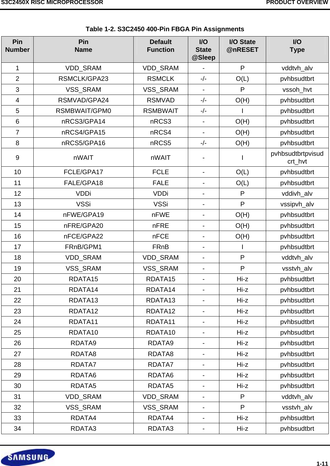
![PRODUCT OVERVIEW S3C2450X RISC MICROPROCESSOR 1-8 Table 1-1. 400-Pin FBGA Pin Assignments − Pin Number Order (2/4) Pin Pin Name Ball Pin Pin Name Ball Pin Pin Name Ball112 VSS_OP2 U7 137 VSS_OP2 Y9 162 SS[1]/GPL14 R13113 nXDACK1/I2CSDA1/GPB7 AC5 138 EINT20/GPG12/ nINPACK R10 163 SS[0]/GPL13 AC14114 nXDREQ1/I2CSCL1/GPB8 AA5 139 EINT21/GPG13/ nREG_CF AC10 164 SPIMISO1/GPL12 Y14115 nXDACK0/I2SSDO_1/GPB9 AB6 140 EINT22/GPG14/ RESET_CF T11 165 SPIMOSI1/GPL11 AB14116 nXDREQ0/I2SSDO_2/GPB10 U8 141 EINT23/GPG15/ CF_PWREN AA10 166 SPICLK1/GPL10 T14 117 VDDiarm Y6 142 VDDiarm AB11 167 SD1_nWP/GPJ15 AC15118 VSSiarm Y7 143 VSSiarm Y10 168 SD1_nCD/GPJ14 U14119 EXTUARTCLK/ GPH12 AC6 144 IICSCL/GPE14 U11 169 SD1_LED/GPJ13/I2S1_LRCK/PCM1_FSYNC AA14120 nCTS0/GPH8 AB7 145 IICSDA/GPE15 AC11 170 SD1_CLK/GPL9 R14121 nRTS0/GPH9 AA6 146 I2SLRCK/GPE0/ AC_nRESET/PCM0_FSYNC AA11 171 VSSi Y15122 TXD0/GPH0 AC7 147 I2SSCLK/GPE1/ AC_SYNC/PCM0_SCLK Y11 172 VDDi T15 123 RXD0/GPH1 AA7 148 I2SCDCLK/GPE2/ AC_BIT_CLK/PCM0_CDCLK R11 173 SD1_CMD/GPL8 AB15124 nCTS1/GPH10 T9 149 I2SSDI/GPE3/ AC_SDI/PCM0_SDI AA12 174 SD1_DAT[0]/GPL0 AC16125 nRTS1/GPH11 AB8 150 I2SSDO_0/GPE4/ AC_SDO/PCM0_SDO T12 175 SD1_DAT[1]/GPL1 AA15126 TXD1/GPH2 U9 151 SPIMISO0/GPE11 AC12 176 SD1_DAT[2]/GPL2 U15127 RXD1/GPH3 AA8 152 SPIMOSI0/GPE12 U12 177 SD1_DAT[3]/GPL3 AA16128 EINT16/GPG8 R9 153 SPICLK0/GPE13 AB12 178 SD1_DAT[4]/GPL4/I2S1_SCLK/PCM1_SCLK R15129 EINT17/GPG9 AB9 154 VDDi Y12 179 SD1_DAT[5]/GPL5/I2S1_CDCLK/PCM1_CDCLK AB16130 VDDiarm AC8 155 VSSi Y13 180 SD1_DAT[6]/GPL6/I2S1_SDI/PCM1_SDI U16131 VSSiarm Y8 156 VSS_SD R12 181 SD1_DAT[7]/GPL7/I2S1_SDO/PCM1_SDO AC17132 EINT18/CAM_FIELD_A/GPG10 T10 157 VDD_SD AC13 182 VDD_SD AA17133 EINT19/GPG11/ nIREQ_CF AA9 158 TXD2/GPH4 T13 183 VSS_SD AB17134 VDD_USBOSC U10 159 RXD2/GPH5 AB13 184 SD0_CLK/GPE5 Y16135 CLKOUT0/GPH13 AC9 160 TXD3/GPH6/nRTS2 U13 185 SD0_CMD/GPE6 AC18136 CLKOUT1/GPH14 AB10 161 RXD3/GPH7/nCTS2 AA13 186 SD0_DAT[0]/GPE7 Y17](https://usermanual.wiki/Diasonic-Technology-Co/RVM-704M.Users-Manual/User-Guide-1826140-Page-42.png)
![S3C2450X RISC MICROPROCESSOR PRODUCT OVERVIEW 1-9 Table 1-1. 400-Pin FBGA Pin Assignments − Pin Number Order (3/4) Pin Pin Name Ball Pin Pin Name Ball Pin Pin Name Ball187 SD0_DAT[1]/GPE8 AB18 228 EINT2/GPF2 R17 269 VDDA33T1 K16188 SD0_DAT[2]/GPE9 AA18 229 EINT3/GPF3 T23 270 VDDI_UDEV J23 189 SD0_DAT[3]/ GPE10 AC19 230 EINT4/GPF4 P15 271 VSSI_UDEV J21 190 VSSA_MPLL AB19 231 EINT5/GPF5 R22 272 SDATA31/GPK15 J22 191 NC Y18 232 EINT6/GPF6 P16 273 SDATA30/GPK14 K15192 VDDA_MPLL AC20 233 EINT7/GPF7 T21 274 SDATA29/GPK13 H23193 VSSA_EPLL AC21 234 PWR_EN R23 275 SDATA28/GPK12 J17 194 EPLLCAP AC22 235 BATT_FLT R20 276 VDD_SDRAM H20195 VDDA_EPLL AA19 236 NRESET P22 277 VSS_SDRAM J16 196 VSSA_ADC AB20 237 TDO P23 278 SDATA27/GPK11 H22197 AIN9 AA20 238 TMS R21 279 SDATA26/GPK10 H21198 AIN8 Y19 239 TDI P17 280 VDDi G23199 AIN7 AC23 240 TCK P20 281 VSSi H17200 AIN6 AB21 241 nTRST N15 282 SDATA25/GPK9 G21201 AIN5 AB22 242 EINT8/GPG0 N22 283 SDATA24/GPK8 F21 202 AIN4 AA22 243 EINT9/GPG1 N16 284 SDATA23/GPK7 G22203 AIN3 AB23 244 EINT10/GPG2 N23 285 SDATA22/GPK6 F23 204 AIN2 AA21 245 EINT11/GPG3 P21 286 SDATA21/GPK5 E23205 AIN1 AA23 246 EINT12/GPG4 N20 287 VDD_SDRAM E20206 AIN0 Y22 247 EINT13/GPG5 N17 288 VSS_SDRAM F22 207 Vref W20 248 EINT14/GPG6 N21 289 SDATA20/GPK4 F20 208 VDDA_ADC Y21 249 EINT15/GPG7 M15 290 SDATA19/GPK3 E21209 VDD_RTC Y23 250 VDD_OP1 M20 291 SDATA18/GPK2 G20210 Xtortc V20 251 DP M23 292 SDATA17/GPK1 D23211 Xtirtc W22 252 DN L23 293 SDATA16/GPK0 E22212 OM[4] Y20 253 VSS_OP1 M21 294 SDATA15 D21213 OM[3] U17 254 nRSTOUT M16 295 SDATA14 C23214 OM[2] W23 255 VDDalive M22 296 VDD_SDRAM C22215 OM[1] V23 256 VSSalive M17 297 VSS_SDRAM D22216 OM[0] V22 257 VDDalive L20 298 SDATA13 B23217 VDDi T16 258 XI_UDEV L21 299 SDATA12 A23218 VSSi W21 259 XO_UDEV L15 300 SDATA11 C21219 VSS_OP3 T17 260 VSSA33C L22 301 SDATA10 B22220 EXTCLK V21 261 VDDA33C L16 302 SDATA9 B21221 VDD_OP3 U22 262 REXT K23 303 SDATA8 B20222 VDDalive U20 263 VDDA33T1 K20 304 SDATA7 A22223 XTIpll R16 264 VSSA33T2 K22 305 SDATA6 A21224 XTOpll U23 265 DM_UDEV L17 306 SDATA5 D20225 VSSalive U21 266 VSSA33T2 K21 307 VDD_SDRAM C20226 EINT0/GPF0 T22 267 DP_UDEV K17 308 VSS_SDRAM D19227 EINT1/GPF1 T20 268 VSSA33T2 J20 309 SDATA4 A20](https://usermanual.wiki/Diasonic-Technology-Co/RVM-704M.Users-Manual/User-Guide-1826140-Page-43.png)
![PRODUCT OVERVIEW S3C2450X RISC MICROPROCESSOR 1-10 Table 1-1. 400-Pin FBGA Pin Assignments – Pin Number Order (4/4) Pin Pin Name Ball Pin Pin Name Ball Pin Pin Name Ball310 SDATA3 B19 341 SADDR3 D15 372 RADDR17/GPA2 G9 311 VSSi C19 342 SADDR4 B13 373 RADDR16/GPA1 A9 312 VDDi A19 343 VDD_SDRAM C13 374 RADDR15 H9 313 SDATA2 B18 344 VSS_SDRAM J13 375 RADDR14 B9 314 SDATA1 D18 345 SADDR5 A13 376 RADDR13 D8 315 SDATA0 C18 346 SADDR6 H13 377 RADDR12 A8 316 VDD_SDRAM G17 347 SADDR7 D14 378 RADDR11 C8 317 VSS_SDRAM A18 348 SADDR8 G12 379 RADDR10 B8 318 DQS1 B17 349 SADDR9 B12 380 VDDi H8 319 DQS0 C17 350 SADDR10 C12 381 VSSi D7 320 DQM3/GPA26 G16 351 SADDR11 A12 382 RADDR9 A7 321 DQM2/GPA25 C16 352 SADDR12 H12 383 RADDR8 C7 322 DQM1 H16 353 VDD_SDRAM D13 384 RADDR7 B7 323 DQM0 A17 354 VSS_SDRAM J12 385 RADDR6 A6 324 nSCS[0] H15 355 SADDR13 D12 386 RADDR5 G8 325 nSCS[1] D17 356 SADDR14 G11 387 VDD_SRAM C6 326 nSWE B16 357 SADDR15 D11 388 VSS_SRAM G7 327 VDD_SDRAM C15 358 VDDi C11 389 RADDR4 B6 328 VSS_SDRAM G15 359 VSSi A11 390 RADDR3 A5 329 SCLK A16 360 nWE_CF/GPA27 B11 391 RADDR2 B5 330 VDD_SDRAM J15 361 nOE_CF/GPA11 H11 392 RADDR1 D6 331 nSCLK B15 362 RADDR25/RDATA_OEN/GPA10 D10 393 RADDR0/GPA0 C5 332 VSS_SDRAM J14 363 RADDR24/GPA9 C10 394 nRBE1 D5 333 SCKE A15 364 RADDR23/GPA8 J11 395 nRBE0 A4 334 VSSi D16 365 RADDR22/GPA7 A10 396 nROE B4 335 VDDi B14 366 RADDR21/GPA6 G10 397 nRWE A3 336 nSRAS G14 367 RADDR20/GPA5 B10 398 nRCS0 A2 337 nSCAS C14 368 VDD_SRAM H10 399 nRCS1/GPA12 A1 338 SADDR0 H14 369 VSS_SRAM D9 400 nRCS2/GPA13 B3 339 SADDR1 A14 370 RADDR19/GPA4 J10 340 SADDR2 G13 371 RADDR18/GPA3 C9](https://usermanual.wiki/Diasonic-Technology-Co/RVM-704M.Users-Manual/User-Guide-1826140-Page-44.png)
![S3C2450X RISC MICROPROCESSOR PRODUCT OVERVIEW 1-15 Pin Number Pin Name Default Function I/O State @SleepI/O State @nRESET I/O Type 143 VSSiarm VSSiarm - P vssicvlh_alv 144 IICSCL/GPE14 GPE14 -/- I pvhbsudtart 145 IICSDA/GPE15 GPE15 -/- I pvhbsudtart 146 I2SLRCK/GPE0/ AC_nRESET/PCM0_FSYNC GPE0 -/-/- I pvhbsudtart 147 I2SSCLK/GPE1/AC_SYNC/ PCM0_SCLK GPE1 -/-/- I pvhbsudtart 148 I2SCDCLK/GPE2/ AC_BIT_CLK0/PCM0_CDCLK GPE2 -/-/- I pvhbsudtart 149 I2SSDI/GPE3/AC_ SDI0/PCM0_SDI GPE3 -/-/- I pvhbsudtart 150 I2SSDO_0/GPE4/AC_SDO0/ PCM0_SDO GPE4 -/-/- I pvhbsudtart 151 SPIMISO0/GPE11 GPE11 -/- I pvhbsudtart 152 SPIMOSI0/GPE12 GPE12 -/- I pvhbsudtart 153 SPICLK0/GPE13 GPE13 -/- I pvhbsudtart 154 VDDi VDDi - P vddivh_alv 155 VSSi VSSi - P vssipvh_alv 156 VSS_SD VSS_SD - P vsstvh_alv 157 VDD_SD VDD_SD - P vddtvh_alv 158 TXD2/GPH4 GPH4 -/- I pvhbsudtart 159 RXD2/GPH5 GPH5 -/- I pvhbsudtart 160 TXD3/GPH6/nRTS2 GPH6 -/-/- I pvhbsudtart 161 RXD3/GPH7/nCTS2 GPH7 -/-/- I pvhbsudtart 162 SS[1]/GPL14 GPL14 -/- I pvhbsudtart 163 SS[0]/GPL13 GPL13 -/- I pvhbsudtart 164 SPIMISO1/GPL12 GPL12 -/- I pvhbsudtart 165 SPIMOSI1/GPL11 GPL11 -/- I pvhbsudtart 166 SPICLK1/GPL10 GPL10 -/- I pvhbsudtart 167 SD1_nWP/GPJ15 GPJ15 -/- I pvhbsudtart 168 SD1_nCD/GPJ14 GPJ14 -/- I pvhbsudtart 169 SD1_LED/GPJ13/I2S1_LRCK/PCM1_FSYNC GPJ13 -/- I pvhbsudtart 170 SD1_CLK/GPL9 GPL9 -/- I pvhbsudtart 171 VSSi VSSi - P vssipvh_alv 172 VDDi VDDi - P vddivh_alv 173 SD1_CMD/GPL8 GPL8 -/- I pvhbsudtart 174 SD1_DAT[0]/GPL0 GPL0 -/- I pvhbsudtart](https://usermanual.wiki/Diasonic-Technology-Co/RVM-704M.Users-Manual/User-Guide-1826140-Page-49.png)
![PRODUCT OVERVIEW S3C2450X RISC MICROPROCESSOR 1-16 Pin Number Pin Name Default Function I/O State @SleepI/O State @nRESET I/O Type 175 SD1_DAT[1]/GPL1 GPL1 -/- I pvhbsudtart 176 SD1_DAT[2]/GPL2 GPL2 -/- I pvhbsudtart 177 SD1_DAT[3]/GPL3 GPL3 -/- I pvhbsudtart 178 SD1_DAT[4]/GPL4/I2S1_ SCLK/PCM1_SCLK GPL4 -/- I pvhbsudtart 179 SD1_DAT[5]/GPL5/I2S1_ CDCLK/PCM1_CDCLK GPL5 -/- I pvhbsudtart 180 SD1_DAT[6]/GPL6/I2S1_ SDI/PCM1_SDI GPL6 -/- I pvhbsudtart 181 SD1_DAT[7]/GPL7/I2S1_ SDO/PCM1_SDO GPL7 -/- I pvhbsudtart 182 VDD_SD VDD_SD - P vddtvh_alv 183 VSS_SD VSS_SD - P vsstvh_alv 184 SD0_CLK/GPE5 GPE5 -/-/- I pvhbsudtart 185 SD0_CMD/GPE6 GPE6 -/-/- I pvhbsudtart 186 SD0_DAT[0]/GPE7 GPE7 -/-/- I pvhbsudtart 187 SD0_DAT[1]/GPE8 GPE8 -/-/- I pvhbsudtart 188 SD0_DAT[2]/GPE9 GPE9 -/-/- I pvhbsudtart 189 SD0_DAT[3]/GPE10 GPE10 -/- I pvhbsudtart 190 VSSA_MPLL VSSA_MPLL - P vsstvlh_alv 191 NC NC 192 VDDA_MPLL VDDA_MPLL - P vddtvlh_alv 193 VSSA_EPLL VSSA_EPLL - P vsstvlh_alv 194 UPLLCAP UPLLCAP - AI pvhbr 195 VDDA_EPLL VDDA_EPLL - P vddtvlh_alv 196 VSSA_ADC VSSA_ADC - P 197 AIN9(XP) AIN9 AI vsstvh_alv 198 AIN8(XM) AIN8 - AI pvhbr 199 AIN7(YP) AIN7 - AI pvhbr 200 AIN6(YM) AIN6 - AI pvhbr 201 AIN5 AIN5 - AI pvhbr 202 AIN4 AIN4 - AI pvhbr 203 AIN3 AIN3 - AI pvhbr 204 AIN2 AIN2 - AI pvhbr 205 AIN1 AIN1 - AI pvhbr 206 AIN0 AIN0 - AI pvhbr 207 Vref Vref - AI pvhbr](https://usermanual.wiki/Diasonic-Technology-Co/RVM-704M.Users-Manual/User-Guide-1826140-Page-50.png)
![S3C2450X RISC MICROPROCESSOR PRODUCT OVERVIEW 1-17 Pin Number Pin Name Default Function I/O State @SleepI/O State @nRESET I/O Type 208 VDDA_ADC VDDA_ADC - P vddtvh_alv 209 VDD_RTC VDD_RTC - P vddrtcvh_alv 210 Xtortc Xtortc - AO pvhsosca 211 Xtirtc Xtirtc - AI pvhsosca 212 OM[4] OM[4] - I pvhbsudtart_alv 213 OM[3] OM[3] - I pvhbsudtart_alv 214 OM[2] OM[2] - I pvhbsudtart_alv 215 OM[1] OM[1] - I pvhbsudtart_alv 216 OM[0] OM[0] - I pvhbsudtart_alv 217 VDDi VDDi - P vddicvlh_alv 218 VSSi VSSi - P vssicvlh_alv 219 VSS_OP3 VSS_OP3 - P vsstvh_alv 220 EXTCLK EXTCLK - I pvhbsudtart 221 VDD_OP3 VDD_OP3 - P vddtvh_alv 222 VDDalive VDDalive - P vddivh_alv 223 XTIpll XTIpll - AI pvhsoscbrt 224 XTOpll XTOpll - AO pvhsoscbrt 225 VSSalive VSSalive - P vssipvh_alv 226 EINT0/GPF0 GPF0 -/- I pvhbsudtart_alv 227 EINT1/GPF1 GPF1 -/- I pvhbsudtart_alv 228 EINT2/GPF2 GPF2 -/- I pvhbsudtart_alv 229 EINT3/GPF3 GPF3 -/- I pvhbsudtart_alv 230 EINT4/GPF4 GPF4 -/- I pvhbsudtart_alv 231 EINT5/GPF5 GPF5 -/- I pvhbsudtart_alv 232 EINT6/GPF6 GPF6 -/- I pvhbsudtart_alv 233 EINT7/GPF7 GPF7 -/- I pvhbsudtart_alv 234 PWR_EN PWR_EN O(L) O(H) pvhbsudtart_alv 235 BATT_FLT BATT_FLT - I pvhbsudtart 236 nRESET nRESET - I pvhbsudtart 237 TDO TDO - O pvhbsudtart 238 TMS TMS - I pvhbsudtart 239 TDI TDI - I pvhbsudtart 240 TCK TCK - I pvhbsudtart 241 nTRST nTRST - I pvhbsudtart 242 EINT8/GPG0 GPG0 -/- I pvhbsudtart_alv 243 EINT9/GPG1 GPG1 -/- I pvhbsudtart_alv](https://usermanual.wiki/Diasonic-Technology-Co/RVM-704M.Users-Manual/User-Guide-1826140-Page-51.png)
![PRODUCT OVERVIEW S3C2450X RISC MICROPROCESSOR 1-20 Pin Number Pin Name Default Function I/O State @SleepI/O State @nRESET I/O Type 316 VDD_SDRAM VDD_SDRAM - P vddtvm_alv 317 VSS_SDRAM VSS_SDRAM - P vsstvm_alv 318 DQS1 DQS1 O(L) Hi-z pvmbsudtbrt 319 DQS0 DQS0 O(L) Hi-z pvmbsudtbrt 320 DQM3/GPA26 DQM3 O(H)- O(L) pvmbsudtbrt 321 DQM2/GPA25 DQM2 O(H) O(L) pvmbsudtbrt 322 DQM1 DQM1 O(H) O(L) pvmbsudtbrt 323 DQM0 DQM0 O(H) O(L) pvmbsudtbrt 324 nSCS[0] nSCS[0] O(H) O(H) pvmbsudtbrt 325 nSCS[1] nSCS[1] O(H) O(H) pvmbsudtbrt 326 nSWE nSWE O(H) O(H) pvmbsudtbrt 327 VDD_SDRAM VDD_SDRAM - P vddtvm_alv 328 VSS_SDRAM VSS_SDRAM - P vsstvm_alv 329 SCLK SCLK O(L) O(SCLK) pvmbsudtbrt 330 VDD_SDRAM VDD_SDRAM - P vddtvm_alv 331 nSCLK nSCLK O(H) O(nSCLK) pvmbsudtbrt 332 VSS_SDRAM VSS_SDRAM P vsstvm_alv 333 SCKE SCKE O(L) O(L) pvmbsudtbrt 334 VSSi VSSi - P vssipvh_alv 335 VDDi VDDi - P vddivh_alv 336 nSRAS nSRAS O(H) O(H) pvmbsudtbrt 337 nSCAS nSCAS O(H) O(H) pvmbsudtbrt 338 SADDR0 SADDR0 - O(L) pvmbsudtbrt 339 SADDR1 SADDR1 - O(L) pvmbsudtbrt 340 SADDR2 SADDR2 - O(L) pvmbsudtbrt 341 SADDR3 SADDR3 - O(L) pvmbsudtbrt 342 SADDR4 SADDR4 - O(L) pvmbsudtbrt 343 VDD_SDRAM VDD_SDRAM - P vddtvm_alv 344 VSS_SDRAM VSS_SDRAM - P vsstvm_alv 345 SADDR5 SADDR5 - O(L) pvmbsudtbrt 346 SADDR6 SADDR6 - O(L) pvmbsudtbrt 347 SADDR7 SADDR7 - O(L) pvmbsudtbrt 348 SADDR8 SADDR8 - O(L) pvmbsudtbrt 349 SADDR9 SADDR9 - O(L) pvmbsudtbrt 350 SADDR10 SADDR10 - O(L) pvmbsudtbrt 351 SADDR11 SADDR11 - O(L) pvmbsudtbrt](https://usermanual.wiki/Diasonic-Technology-Co/RVM-704M.Users-Manual/User-Guide-1826140-Page-54.png)
![PRODUCT OVERVIEW S3C2450X RISC MICROPROCESSOR 1-24 4.1 SIGNAL DESCRIPTIONS Table 1-4. S3C2450 Signal Descriptions Signal In/Out Description Reset, Clock & Power XTIpll AI Crystal input signals for internal osc circuit. When OM[0] = 0, XTIpll is used for MPLL CLK source and EPLL CLK source. If it isn't used, it has to be Low (0V) XTOpll AO Crystal output signals for internal osc circuit. When OM[0] = 0, XTIpll is used for MPLL CLK source and EPLL CLK source. If it isn't used, it has to be float NC AI Not connected. EPLLCAP AI Loop filter capacitor for Extra PLL XTIrtc AI 32.768 kHz crystal input for RTC. If it isn’t used, it has to be High (VDD_RTC=3.3V). XTOrtc AO 32.768 kHz crystal output for RTC. If it isn’t used, it has to be float. CLKOUT[1:0] O Clock output signal. The CLKSEL of MISCCR(GPIO register) register configures the clock output mode among the MPLL_CLK, EPLL CLK, ARMCLK, HCLK, PCLK. nRESET ST nRESET suspends any operation in progress and places S3C2450 into a known reset state. For a reset, nRESET must be held to L level for at least 4 OSCin after the processor power has been stabilized. nRSTOUT O For external device reset control (nRSTOUT = nRESET & nWDTRST & SW_RESET) *SW_RESET = nRSTCON of GPIO MISCCR PWREN O core power on-off control signal nBATT_FLT I Probe for battery state (Does not wake up at Sleep mode in case of low battery state). If it isn’t used, it has to be High (3.3V). OM[4:0] I OM[4:0] set operating modes of S3C2450 Refer to “S3C2450 Operation Mode Description Table” EXTCLK I External clock source. When OM[0] = 1, EXTCLK is used for MPLL and EPLL CLK source. If it isn't used, it has to be Low (0V). Memory Interface (ROM/SRAM/NAND/CF) RADDR[25:0] O RADDR[25:0] (Address Bus) outputs the memory address of the corresponding bank . RDATA[15:0] IO RDATA[15:0] (Data Bus) inputs data during memory read and outputs data during memory write. The bus width is programmable among 8/16-bit. nRCS[5:0] O nRCS[5:0] (Chip Select) are activated when the address of a memory is within the address region of each bank. The number of access cycles and the bank size can be programmed. nRWE O nRWE (Write Enable) indicates that the current bus cycle is a write cycle.nROE O nOE (Output Enable) indicates that the current bus cycle is a read cycle.](https://usermanual.wiki/Diasonic-Technology-Co/RVM-704M.Users-Manual/User-Guide-1826140-Page-58.png)
![S3C2450X RISC MICROPROCESSOR PRODUCT OVERVIEW 1-25 Signal In/Out Description nRBE[1:0] O Upper byte/lower byte enable (In case of 16-bit SRAM) nWAIT I nWAIT requests to prolong a current bus cycle. As long as nWAIT is L, the current bus cycle cannot be completed. If nWAIT signal isn’t used in your system, nWAIT signal must be tied on pull-up resistor. SDRAM I/F SADDR[15:0] O SDRAM Address bus SDATA[31:0] IO SDRAM Data Bus nSRAS O SDRAM row address strobe nSCAS O SDRAM column address strobe nSWE O SDRAM write enable nSCS[1:0] O SDRAM chip select DQM[3:0] O SDRAM data mask DQS[1:0] O mDDR/DDR2 Data Strobe SCLK O SDRAM clock nSCLK O mDDR/DDR2 Conversion clock SCKE O SDRAM clock enable NAND Flash FCLE O Command latch enable FALE O Address latch enable nFCE O Nand flash chip enable nFRE O Nand flash read enable nFWE O Nand flash write enable FRnB I Nand flash ready/busy SMC/OneNAND RSMCLK I/O SMC Clock RSMVAD O SMC Address Valid RSMBWAIT O SMC Burst Wait CF I/F nOE_CF O CF Output Enable Strobe nWE_CF O CF Write Enable Strobe nIREQ_CF I Interrupt request from CF card nINPACK_CF I Input acknowledge in I/O mode CardPWR_CF O Card Power Enable nREG_CF O Register in CF card strobe RESET_CF O CF card reset LCD Control Unit RGB_VD/SYS_VD[23:0] O RGB I/F Video Data: RGB_VD[23:0] i80 I/F Video DataSYS_VD[17:0]](https://usermanual.wiki/Diasonic-Technology-Co/RVM-704M.Users-Manual/User-Guide-1826140-Page-59.png)
![PRODUCT OVERVIEW S3C2450X RISC MICROPROCESSOR 1-26 Signal In/Out Description RGB_VCLK/SYS_WR O RGB I/F LCD Clock i80 I/F Write Enable RGB_VSYNC/SYS_CS1 O RGB I/F Vertical Sync. Signal i80 I/F Sub LCD Select RGB_HSYNC/SYS_CS0 O RGB I/F Horizontal Sync. Signal i80 I/F Main LCD Select RGB_VDEN/SYS_RS O RGB I/F Data Enable i80 I/F Register/ State select RGB_LEND/SYS_OE O RGB I/F Line End Signal i80 I/F Output Enable CAMERA Interface CAMRESET O Camera interface reset CAMCLKOUT O Camera interface master clock CAMPCLK I Camera interface pixel clock CAMHREF I Camera interface horizontal sync CAMVSYNC I Camera interface horizontal sync CAMDATA[7:0] I Camera interface data CAM_FIELD_A I Interlace field (only used in interlace mode) Interrupt Control Unit EINT[23:0] I External interrupt request External I/F nXDREQ[1:0] I External DMA request nXDACK[1:0] O External DMA acknowledge nXBREQ I nXBREQ (Bus Hold Request) allows another bus master to request control of the local bus. nXBACK active indicates that bus control has been granted. nXBACK O nXBACK (Bus Hold Acknowledge) indicates that the S3C2450 has surrendered control of the local bus to another bus master. UART RXD[3:0] I UART receives data input (ch. 0/1/2) TXD[3:0] O UART transmits data output (ch. 0/1/2) nCTS[2:0] I UART clear to send input signal (ch. 0/1) nRTS[2:0] O UART request to send output signal (ch. 0/1) EXTUARTCLK I External clock input for UART TSADC AIN[9:0] AI ADC input [9:0]. If do not use ADC function, AIN [9] and AIN [7] pins are tied to VDDA_ADC. Others are tied to GND. When touch screen device is used, A[6], A[7] , A[8] and A[9] are used as YM, YP, XM and XP, respectively.](https://usermanual.wiki/Diasonic-Technology-Co/RVM-704M.Users-Manual/User-Guide-1826140-Page-60.png)
![PRODUCT OVERVIEW S3C2450X RISC MICROPROCESSOR 1-28 Signal In/Out Description DN IO DATA(–) from USB host. (Need to 15kΩ pull-down) DP IO DATA(+) from USB host. (Need to 15kΩ pull-down) USB Device DM_UDEV IO DATA(–) for USB peripheral. DP_UDEV IO DATA(+) for USB peripheral. REXT O External Resistor ( 44.2ohm +/- 1%) XO_UDEV OSC Crystal output XI_UDEV OSC Crystal input SPI SPIMISO[1:0] IO SPIMISO is the master data input line, when SPI is configured as a master. When SPI is configured as a slave, these pins reverse its role. SPIMOSI[1:0] IO SPIMOSI is the master data output line, when SPI is configured as a master. When SPI is configured as a slave, these pins reverse its role. SPICLK[1:0] IO SPI clock nSS[1:0] I SPI chip select (only for slave mode) SDMMC Interface SD1_DAT[7:0] IO SD1 receive/transmit data SD1_CMD IO SD1 receive response/ transmit command SD1_CLK O SD1 clock SD1_nWP O SD1 Write Protect SD1_nCD O SD1 Card Detect SD1_nLED O SD1 LED SD0_DAT[3:0] IO SD0 receive/transmit data SD0_CMD IO SD0 receive response/ transmit command SD0_CLK O SD0 clock General Port GPn[173:0] IO General input/output ports, which are multiplexed with other function pins (some ports are output only). TIMMER/PWM TOUT[3:0] O Timer output[3:0] TCLK I External timer clock input JTAG TEST LOGIC nTRST I nTRST (TAP Controller Reset) resets the TAP controller at start. If debugger is used, A 10K pull-up resistor has to be connected. If debugger (black ICE) is not used, nTRST pin must be issued by a low active pulse (Typically connected to nRESET). TMS I TMS (TAP Controller Mode Select) controls the sequence of the TAP controller's states.](https://usermanual.wiki/Diasonic-Technology-Co/RVM-704M.Users-Manual/User-Guide-1826140-Page-62.png)
![S3C2450X RISC MICROPROCESSOR PRODUCT OVERVIEW 1-31 4.2 S3C2450 OPERATION MODE DESCRIPTION Table 1-5. S3C2450 Operation Mode Description OM[4] OM[3] OM[2] OM[1] OM[0] OM[4] OM[3] OM[2] OM[1] OM[0] Operation Mode 0 X-TAL 0 1 0 0 1 iROM EXTCLK iROM 0 Reserved Reserved0 1 JTAG JTAG 0 X-TAL 0 1 1 OneNAND(Muxed) 16-bit EXTCLK OneNAND(Muxed) 0 X-TAL 0 1 8-bit EXTCLK 0 X-TAL 1 0 1 1 1 OneNAND/ ROM ROM/ OneNAND(Demuxed) 16-bit EXTCLK ROM/ OneNAND(Demuxed) * OM[0] selects the clock source of MPLL/EPLL ( You can select different EPLL clock source with that of MPLL by software setting – refer to SYSCON)](https://usermanual.wiki/Diasonic-Technology-Co/RVM-704M.Users-Manual/User-Guide-1826140-Page-65.png)
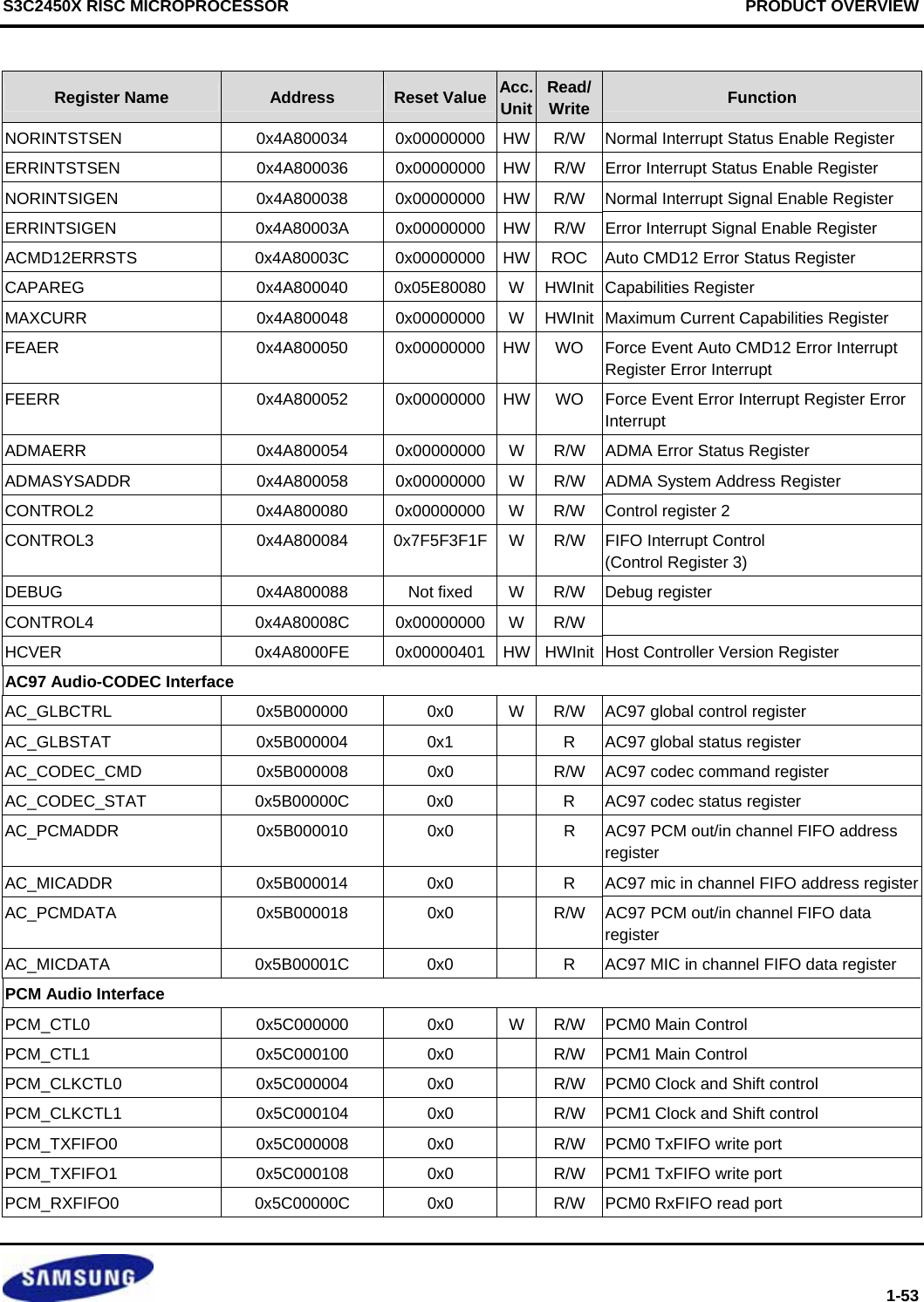
![S3C2450X RISC MICROPROCESSOR PRODUCT OVERVIEW 1-55 Register Name Address Reset ValueAcc. Unit Read/Write Function CW_RB_X_REG 0x4D408234 0x0000_0000 R/W Right X coordinate of Clip Window. CW_RB_Y_REG 0x4D408238 0x0000_0000 R/W Bottom Y coordinate of Clip Window. COORD0_REG 0x4D408300 0x0000_0000 R/W Coordinates 0 register. COORD0_X_REG 0x4D408304 0x0000_0000 R/W X coordinate of Coordinates 0. COORD0_Y_REG 0x4D408308 0x0000_0000 R/W Y coordinate of Coordinates 0. COORD1_REG 0x4D408310 0x0000_0000 R/W Coordinates 1 register. COORD1_X_REG 0x4D408314 0x0000_0000 R/W X coordinate of Coordinates 1. COORD1_Y_REG 0x4D408318 0x0000_0000 R/W Y coordinate of Coordinates 1. COORD2_REG 0x4D408320 0x0000_0000 R/W Coordinates 2 register. COORD2_X_REG 0x4D408324 0x0000_0000 R/W X coordinate of Coordinates 2. COORD2_Y_REG 0x4D408328 0x0000_0000 R/W Y coordinate of Coordinates 2. COORD3_REG 0x4D408330 0x0000_0000 R/W Coordinates 3 register. COORD3_X_REG 0x4D408334 0x0000_0000 R/W X coordinate of Coordinates 3. COORD3_Y_REG 0x4D408338 0x0000_0000 R/W Y coordinate of Coordinates 3. ROT_OC_REG 0x4D408340 0x0000_0000 R/W Rotation Origin Coordinates. ROT_OC_X_REG 0x4D408344 0x0000_0000 R/W X coordinate of Rotation Origin Coordinates. ROT_OC_Y_REG 0x4D408348 0x0000_0000 R/W Y coordinate of Rotation Origin Coordinates. ROTATE_REG 0x4D40834C 0x0000_0001 R/W Rotation Mode register. X_INCR_REG 0x4D408400 0x0000_0000 R/W X Increment register. Y_INCR_REG 0x4D408404 0x0000_0000 R/W Y Increment register. ROP_REG 0x4D408410 0x0000_0000 R/W Raster Operation register. ALPHA_REG 0x4D408420 0x0000_0000 R/W Alpha value, Fading offset. FG_COLOR_REG 0x4D408500 0x0000_0000 R/W Foreground Color / Alpha register. BG_COLOR_REG 0x4D408504 0x0000_0000 R/W Background Color register BS_COLOR_REG 0x4D408508 0x0000_0000 R/W Blue Screen Color register SRC_COLOR_MODE_REG 0x4D408510 0x0000_0000 R/W Src Image Color Mode register. DEST_COLOR_MODE_REG 0x4D408514 0x0000_0000 R/W Dest Image Color Mode register PATTERN_REG[0:31] 0x4D408600 ~ 0x4D80867C 0x0000_0000 R/W Pattern memory. PATOFF_REG 0x4D408700 0x0000_0000 R/W Pattern Offset XY register. PATOFF_X_REG 0x4D408704 0x0000_0000 R/W Pattern Offset X register. PATOFF_Y_REG 0x4D408708 0x0000_0000 R/W Pattern Offset Y register. STENCIL_CNTL_REG 0x4D408720 0x0000_0000 R/W Stencil control register STENCIL_DR_MIN_REG 0x4D408724 0x0000_0000 W Stencil decision reference MIN register STENCIL_DR_MAX_REG 0x4D408728 0xFFFF_FFFF W Stencil decision reference MAX register SRC_BASE_ADDR_REG 0x4D408730 0x0000_0000 R/W Source Image Base Address register](https://usermanual.wiki/Diasonic-Technology-Co/RVM-704M.Users-Manual/User-Guide-1826140-Page-89.png)

![SYSTEM CONTROLLER S3C2450X RISC MICROPROCESSOR 2-4 POWERnRESETEXTCLKor XTIpllVCOoutputSYSCLKPLL is configured by S/W first timeLock timeVCO is adapte to new clock frequency.The logic is operarted byEXTCLK or XTIpll SYSCLK is FOUTClockdisable Figure 2-2. Power-On Reset Sequence 4.3 WATCHDOG RESET Watchdog reset is invoked when software fails to prevent the watchdog timer from timing out. During the watchdog reset, the following actions occur : • All units(except some blocks listed in table 2-1 ) go into their pre-defined reset state. • All pins get their reset state, and BATT_FLT pin is ignored. • The nRSTOUT pin is asserted during watchdog reset. Watchdog reset can be activated in normal and idle mode because watchdog timer can expire with clock. Watchdog reset is invoked when watchdog timer and reset are enabled (WTCON[5] = 1, WTCON[0]=1) and watchdog timer is expired. Watchdog reset is invoked then, the following sequence occurs. : 1. Watchdog reset source asserts. 2. Internal reset signals and nRSTOUT are asserted and reset counter is activated. 3. Reset counter is expired then, internal reset signals and nRSTOUT are deasserted.](https://usermanual.wiki/Diasonic-Technology-Co/RVM-704M.Users-Manual/User-Guide-1826140-Page-96.png)
![S3C2450X RISC MICROPROCESSOR SYSTEM CONTROLLER 2-5 4.4 SOFTWARE RESET Software can initialize the device state itself when it writes “0x533C_2450” to SWRST register. During the software reset, the following actions occur : • All units(except some blocks listed in table 2-1 ) go into their pre-defined reset state. • All pins get their reset state, and BATT_FLT pin is ignored. • The nRSTOUT pin is asserted during software reset. Software reset is invoked then, the following sequence occurs. : 1. User write “0x533C_2450” to SWRST register. 2. System controller request bus controller to finish current transactions. 3. Bus controller send acknowledge to system controller after completed bus transactions. 4. System controller request memory controller to enter into self refresh mode. 5. System controller wait for self refresh acknowledge from memory controller. 6. Internal reset signals and nRSTOUT are asserted and reset counter is activated. 7. Reset counter is expired then, internal reset signals and nRSTOUT are deasserted. 4.5 WAKEUP RESET When S3C2450 is woken up from SLEEP mode by wakeup event, the wakeup reset is invoked. The detail description will be explained in the power management mode section. Table 2-1 lists alive registers which are not influenced various reset sources except nRESET. With the exception of below registers (in table 2-1), All S3C2450’s internal registers are reset by above-mentioned reset sources. Table 2-1. Registers & GPIO Status in RESET (R: reset, S: sustain previous value) Region Registers Software Wakeup Watchdog nRESET SYSCON OSCSET , PWRCFG, RSTCON, RSTSTAT, WKUPSTAT, INFORM0, INFORM1, INFORM2, INFORM3 S S S R GPIO GPFCON, GPFUDP, GPFDAT, GPGCON[7:0], GPGUDP, GPGDAT[7:0], EXTINT0 ~ EXTINT15 R S R R](https://usermanual.wiki/Diasonic-Technology-Co/RVM-704M.Users-Manual/User-Guide-1826140-Page-97.png)
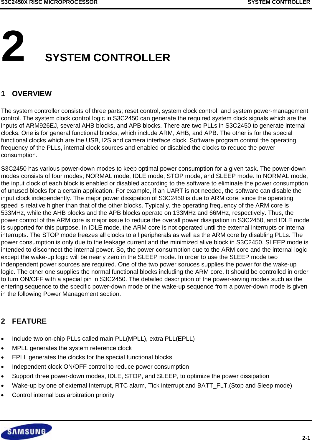
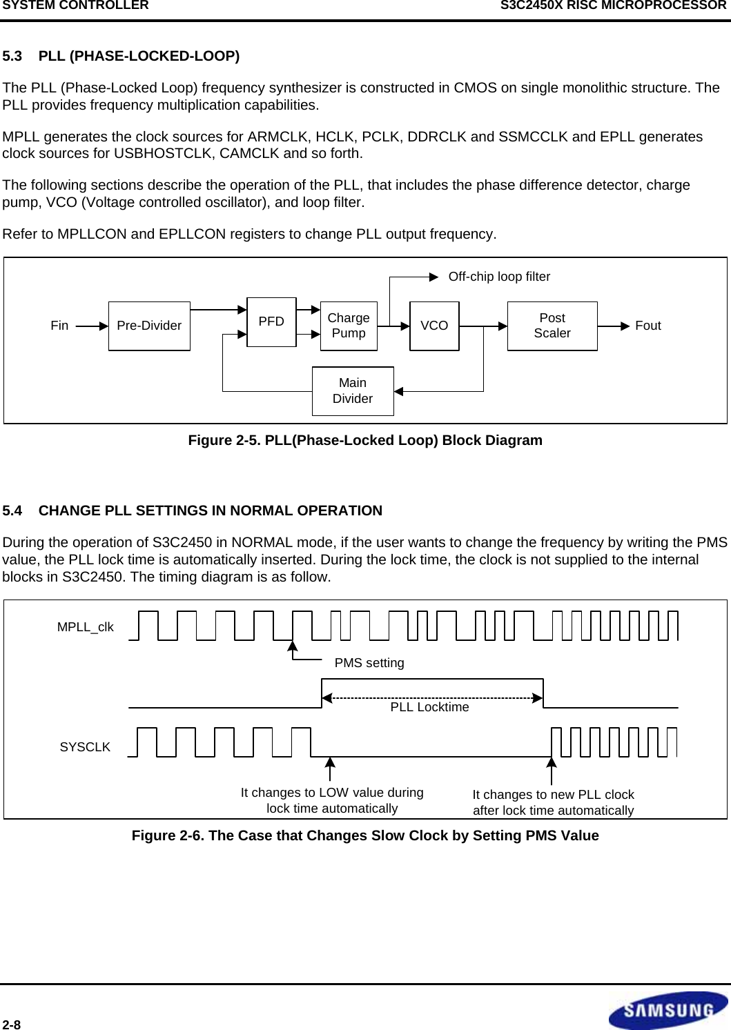
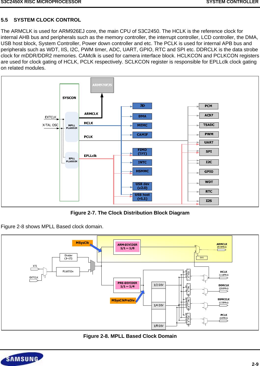
![SYSTEM CONTROLLER S3C2450X RISC MICROPROCESSOR 2-6 5 CLOCK MANAGEMENT 5.1 CLOCK GENERATION OVERVIEW Figure 2-3 shows the block diagram of the clock generation module. The main clock source comes from an external crystal (XTI) or external clock (EXTCLK). EPLL’s input clock is one of the XTI or EXTCLK. Clock selection can be done by configuring MUX selection signal. When both XTI and EXTCLK are running, GFM(Glitch Free Mux)’s output can be configured easily without generating glitch. But if you change or select EPLL input clock when either XTI or EXTCLK is running, disabled clock should be have logic LOW. XTI clock source can be reference of PLL after oscillated at PAD. User can configure stabilization time by setting OSCSET register and ON/OFF when power-down mode by setting PWRCFG register. The clock generator consists of two PLLs (Phase-Locked-Loop) which generate the high-frequency clock signals required in S3C2450. MPLLExtClk DivXTIEXTCLKOM[0]ARMCLKHCLKPCLKDDRCLKSYSCLKEPLLXTIEXTCLK ECLK USBHOSTCAMCLKI2SCLKUARTCLKLCDCLKOM[0]&CLKSRCClock Divider &Mux Figure 2-3. Clock Generator Block Diagram 5.2 CLOCK SOURCE SELECTION Table 2-2 and 2-3 show the relationship between the combination of mode control pins OM[0] and the selection of source clock for S3C2450. Table 2-2. Clock source selection for the main PLL and clock generation logic OM[0] MPLL Reference Clock (Main clock source) 0 XTI 1 EXTCLK](https://usermanual.wiki/Diasonic-Technology-Co/RVM-704M.Users-Manual/User-Guide-1826140-Page-98.png)
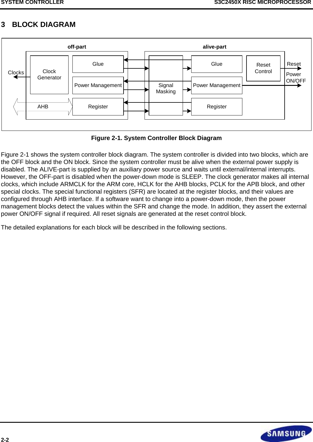
![S3C2450X RISC MICROPROCESSOR SYSTEM CONTROLLER 2-7 Table 2-3. Clock Source Selection for the EPLL CLKSRC[8] (register) CLKSRC[7] (register) OM[0] EPLL Reference Clock 0 X 0 XTI 0 X 1 EXTCLK 1 0 X XTI 1 1 X EXTCLK Table 2-4. PLL & Clock Generator Condition MPLLCAP : N/A Loop filter capacitance CLF EPLLCAP : Typical 1.8nF 5% Fin - MPLL: 10 − 30 MHz EPLL: 10 − 40 MHz Fout - MPLL: 40 − 1600 MHz EPLL: 20 − 600 MHz External capacitance used for X-tal CEXT 15 pF Feedback Resistor used for X-tal RF 1MΩ Figure 2-4. Main Oscillator Circuit Examples](https://usermanual.wiki/Diasonic-Technology-Co/RVM-704M.Users-Manual/User-Guide-1826140-Page-99.png)
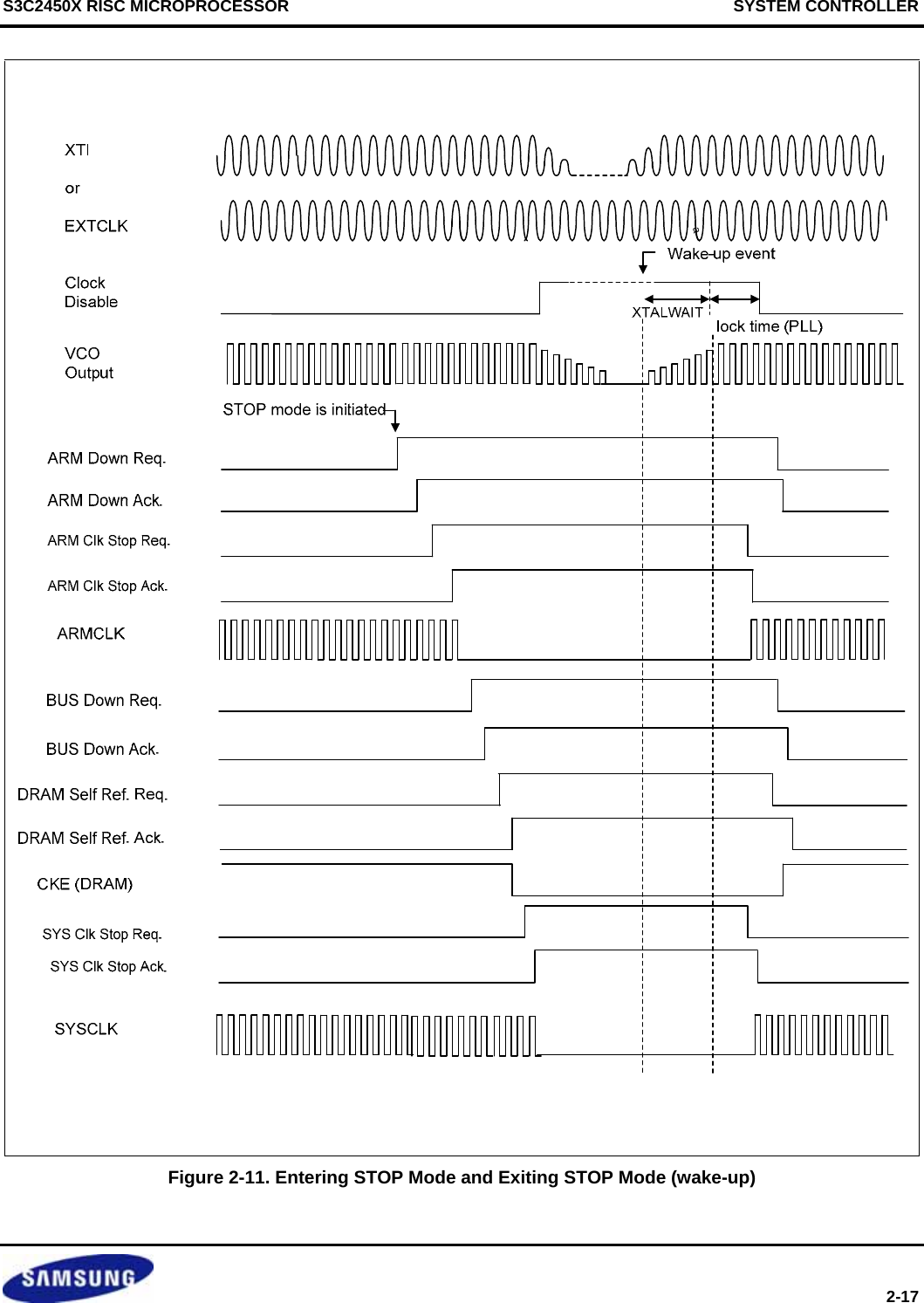
![SYSTEM CONTROLLER S3C2450X RISC MICROPROCESSOR 2-14 6.2 POWER SAVING MODES S3C2450 can support various power saving modes. These are Normal mode, idle mode, Stop mode, Deep-stop mode and Sleep mode. 6.2.1 Normal Mode (General Clock Gating Mode) In General Clock Gating mode, the On/Off clock gating of the individual clock source of each IP block is performed by controlling of each corresponding clock source enable bit. The Clock Gating is applied instantly whenever the corresponding bit (or bits) is changed. (these bits are set or cleared by the main CPU.) 6.2.2 IDLE Mode In IDLE mode, the clock to CPU core is stopped. To enter the idle mode, User must use ARM926EJ CP15 command (MCR p15, 0, Rd, c7, c0, 4). If user order this command, ARM core prepare to enter into power down mode. These are draining write buffer, letting memory system is in a quiescent state and confirming all external interface(AHB interface) is in idle state. After completing above operation, ARM asserted STANBYWFI signal. So, System Controller of S3C2450 check STANDBYWFI signal is asserted and disabe ARM clock. By doing that, System can go into idle mode safely. To exit the idle mode, All interrupt sources, RTC ALARM, RTC Tick Counter, Battery Fault signal should be activated. 6.2.3 STOP mode (Normal and Deep-stop) In STOP mode, all clocks are stopped for minimum power consumption. Therefore, the PLL and oscillator circuit are also stopped(oscillator circuit is stopped optionally, see PWRCFG register). The STOP Mode is activated after the execution of the STORE instruction that enables the STOP Mode bit. The STOP Mode bit should be cleared after the wake-up from the STOP state for the entering of next STOP Mode. The H/W logic only detects the low-to-high triggering of the STOP Mode bit. In Deep-STOP mode ARM core’s power is off by using internal power gating. By this way, the static current will be reduced remarkably compared with STOP mode. To enter the Deep-STOP mode, PWRMODE[18] register should be configured before entering STOP mode. After waking up from Deep-STOP mode, System controller resets ARM core only. To exit from STOP mode, External interrupt, RTC alarm, RTC Tick, or nRESET has to be activated. During the wake-up sequences, the crystal oscillator and PLL may begin to operate. The crystal-oscillator settle-down-time and the PLL locking-time is required to provide stabilized ARMCLK. Those time-waits are automatically inserted by the hardware of S3C2450. During these time-waits, the clock is not supplied to the internal logic circuitry. STOP mode Entering sequence is as follows 1. Set the STOP Mode bit (by the main CPU) 2. System controller requests bus controller to finish bus transactions of ARM Core. 3. System controller disable ARM clock after getting ARM Down acknowledge. 4. System controller requests bus controller to finish current transactions. 5. Bus controller send acknowledge to system controller after completed bus transactions.](https://usermanual.wiki/Diasonic-Technology-Co/RVM-704M.Users-Manual/User-Guide-1826140-Page-106.png)
![S3C2450X RISC MICROPROCESSOR SYSTEM CONTROLLER 2-15 6. System controller request memory controller to enter self refresh mode. It is for preserving contents in SDRAM. 7. System controller wait for self refresh acknowledge from memory controller. 8. After receiving the self-refresh acknowledge, system controller disables system clocks, and switches SYSCLK’s source to MPLL reference clock. 9. Disables PLLs and Crystal(XTI) oscillation. If OSC_EN_STOP bit in PWRCFG register is ‘high’ then system controller doesn’t disable crystal oscillation. 10. When PWRMODE[18] register is configured as ‘1’ (Deep-STOP Enabled), ARM_PWRENn signal change to enable ARM power gating. ARM Core is reset state during STOP mode. STOP mode Exiting sequence is as follows 1. Enable X-tal Oscillator if it is used, and wait the OSC settle down (around 1ms). 2. After the Oscillator settle-down, the System Clock is fed using the PLL input clock and also enable the PLLs and waits the PLL locking time 3. Switching the clock source, now the PLL is the clock source. 4. When waking up from Deep-STOP mode, ARM_PWRENn is restored to release ARM power gating. After producing SYSCLK ARM_RESETn will be released to let ARM work normally. NOTE DRAM has to be in self-refresh mode during STOP and SLEEP mode to retain valid memory data. LCD must be stopped before STOP and SLEEP mode, because DRAM can't be accessed when it is in self-refresh mode.](https://usermanual.wiki/Diasonic-Technology-Co/RVM-704M.Users-Manual/User-Guide-1826140-Page-107.png)
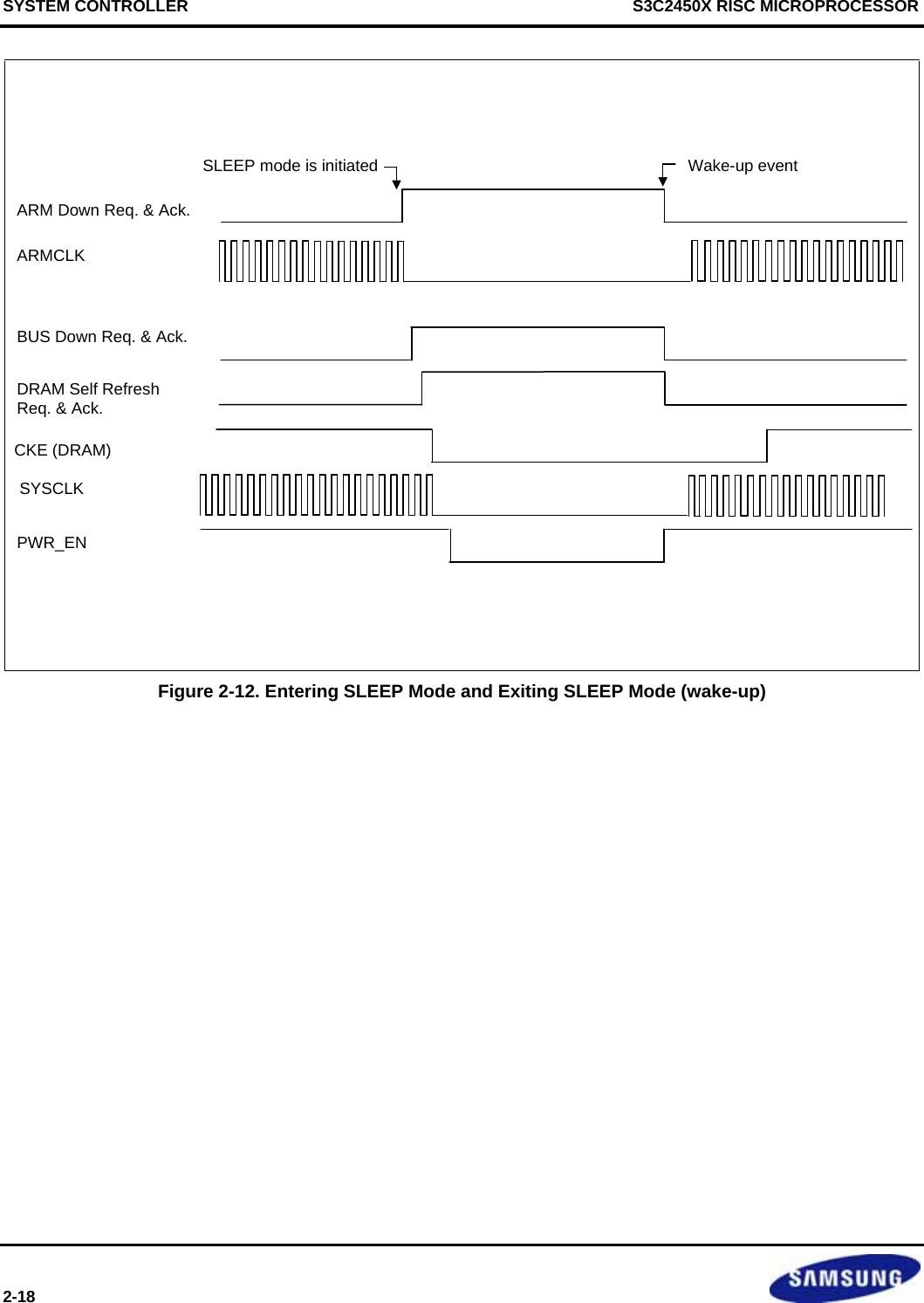
![SYSTEM CONTROLLER S3C2450X RISC MICROPROCESSOR 2-16 6.2.4 SLEEP MODE In the SLEEP Mode, all the clock sources are off and also the internal logic-power is not supplied except for the wake-up logic circuitry. In this mode, the static power-dissipation of internal logic can be minimized. SLEEP Mode Entering sequence is as follows. 1. User writes command into the system controller’s PWRMODE[15:0] register to let system enter into the SLEEP Mode. 2. System controller requests bus controller to finish bus transactions of ARM Core. 3. System controller disable ARM clock after getting ARM Down acknowledge. 4. System controller requests bus controller to finish current transactions. 5. Bus controller send acknowledge to system controller after completed bus transactions. 6. System controller request memory controller to enter self refresh mode. It is for preserving contents in SDRAM. 7. System controller wait for self refresh acknowledge from memory controller. 8. After receiving the self-refresh acknowledge, System controller disable system clocks(HCLK, PCLK and so on). 9. System controller asserts control signals to mask unknown state of ALIVE logics and to preserve data of retention Pads. 10. System controller asserts PWR_EN pin and disables the X-tal and PLL oscillation. PWR_EN pin is used to indicate the readiness for external power OFF and to enable and disable of of the power regulator which produces internal-logic power. SLEEP Mode Exiting sequence is as follows. 1. System controller enable external power source by deactivation of the PWR_EN pin and wait power settle down time (it is programmable by a register in the PWRSETCNT field of RSTCON register). 2. System controller asserts HRESETn and consequently all bus down, self refresh requests and acknowledge signals will be their reset state. 3. System controller release the HRESETn(synchronously, relatively to the system clock) after the power supply is stabilized.](https://usermanual.wiki/Diasonic-Technology-Co/RVM-704M.Users-Manual/User-Guide-1826140-Page-108.png)
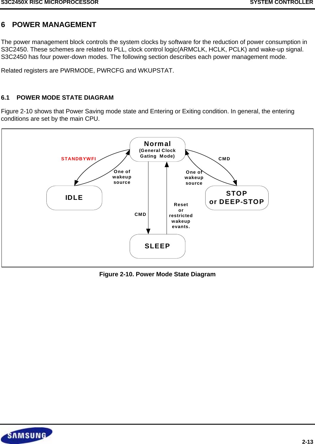
![SYSTEM CONTROLLER S3C2450X RISC MICROPROCESSOR 2-20 6.5 POWER SAVING MODE ENTERING/EXITING CONDITION Table 2-8 shows that Power Saving mode state and Entering or Exiting condition. In general, the entering conditions are set by the main CPU. Pleas refer to power-related registers(PWRMODE, PWRCFG and WKUPSTAT) before adopting power saving scheme on your system. In dealing with sleep mode, It is good for you to know following two restrictions. To enter sleep mode by BATT_FLT, you have to configure BATF_CFG bits of PWRCFG register. Not to exit from sleep mode when BATT_FLT is LOW, you have to configure SLEEP_CFG bit of PWRCFG register. Table 2-8. Power Saving Mode Entering/Exiting Condition Power down mode Enter Exit Clock Gating at NORMAL Clear a respective clock on/off bit for each IP to save power. Set a respective clock on/off bit for each IP to operate normally IDLE STANDBYWFI 1. All interrupt sources 2. RTC alarm 3. RTC Tick 4. BATT_FLT STOP CMD 1. EINT[15:0] (External Interrupt) 2. RTC alarm 3. RTC Tick 4. BATT_FLT SLEEP CMD 1. EINT[15:0] (External Interrupt) 2. RTC alarm 3. RTC Tick 4. BATT_FLT](https://usermanual.wiki/Diasonic-Technology-Co/RVM-704M.Users-Manual/User-Guide-1826140-Page-112.png)
![SYSTEM CONTROLLER S3C2450X RISC MICROPROCESSOR 2-22 8 INDIVIDUAL REGISTER DESCRIPTIONS 8.1 CLOCK SOURCE CONTROL REGISTERS (LOCKCON0, LOCKCON1, OSCSET, MPLLCON, AND EPLLCON) The six registers control two internal PLLs and an external oscillator. The output frequency of the PLL is determined by the divider values of MPLLCON and EPLLCON. The stabilization time for PLLs and the oscillator is controlled by LOCKCON0/1 and OSCSET, respectively. Register Address R/W Description Reset Value LOCKCON0 0x4C00_0000 R/W MPLL lock time count register 0x0000_FFFF LOCKCON1 0x4C00_0004 R/W EPLL lock time count register 0x0000_FFFF OSCSET 0x4C00_0008 R/W Oscillator stabilization control register 0x0000_8000 MPLLCON 0x4C00_0010 R/W MPLL configuration register 0x0185_40C0 EPLLCON 0x4C00_0018 R/W EPLL configuration register 0x0120_0102 EPLLCON_K 0x4C00_001C R/W EPLL configuration register for K value 0x0000_0000 Conventional PLL requires stabilization duration after the PLL is ON. The duration can be varied according to the device variation. Thus, software must adjust these fields with appropriate values in the LOCKCON0/1 register whose values mean the number of the external reference clock. LOCKCON0 Bit Description Initial ValueRESERVED [31:16] RESERVED 0x0000 M_LTIME [15:0] MPLL lock time count value for ARMCLK, HCLK, and PCLK Typically, M_LTIME must be longer than 300 usec. 0xFFFF LOCKCON1 Bit Description Initial ValueRESERVED [31:16] RESERVED 0x0000 E_LTIME [15:0] EPLL lock time count value for UARTCLK, SPICLK and etc. Typically, E_LTIME must be longer than 300 usec. 0xFFFF In general, an oscillator requires stabilization time. This register specifies the duration based on the reference clock. OSCSET Bit Description Initial ValueRESERVED [31:0] RESERVED 0x0000 XTALWAIT [15:0] Crystal oscillator settle-down wait time, this value is valid when s3c2450 is wakeup by stop mode 0x8000](https://usermanual.wiki/Diasonic-Technology-Co/RVM-704M.Users-Manual/User-Guide-1826140-Page-114.png)
![S3C2450X RISC MICROPROCESSOR SYSTEM CONTROLLER 2-23 MPLLCON Bit Description Initial ValueRESERVED [31:26] - 0x00 MPLLEN_STOP [25] MPLL ON/OFF in STOP mode. 0:OFF, 1:ON 0 ONOFF [24] MPLL ON/OFF. 0:ON, 1:OFF 1 MDIV [23:14] Main divider value of MPLL 0x215 RESERVED [13:11] - 0x0 PDIV [10:5] Pre-divider value of MPLL 0x6 RESERVED [4:3] - 0x0 SDIV [2:0] Post-divider value of MPLL 0x0 The output frequencies of MPLL can be calculated using the following equations: FOUT = (m x FIN) / (p x 2S) (should be 40~1600MHz) Fvco = (m x FIN) / p (should be 800~1600MHz) where, m = MDIV, p = PDIV, s = SDIV, Fin = 10~30Mhz Don't set the value PDIV[5:0] or MDIV[9:0] to all zeros. (6’b00 0000 / 10’b00 0000 0000) NOTE Although there is the equation for choosing PLL value, we strongly recommend only the values in the PLL value recommendation table. If you have to use other values, please contact us. FIN (MHz) Target FOUT (MHz) MDIV (decimal) PDIV (decimal) SDIV (decimal) Duty 12 240 320 4 2 40~60% 12 400 400 3 2 40~60% 12 450 225 3 1 40~60% 12 500 250 3 1 40~60% 12 534 267 3 1 40~60% 12 600 300 3 1 40~60% 12 800 400 3 1 40~60%](https://usermanual.wiki/Diasonic-Technology-Co/RVM-704M.Users-Manual/User-Guide-1826140-Page-115.png)
![SYSTEM CONTROLLER S3C2450X RISC MICROPROCESSOR 2-24 EPLLCON Bit Description Initial Value RESERVED [31:26] - 0x00 EPLLEN_STOP [25] EPLL ON/OFF in STOP mode. 0:OFF, 1:ON 0 ONOFF [24] EPLL ON/OFF. 0:ON, 1:OFF 1 MDIV [23:16] EPLL main divider value 0x20 RESERVED [15:14] - 0x0 PDIV [13:8] EPLL pre-divider value 0x1 RESERVED [7:3] - 0x00 SDIV [2:0] EPLL post-scaler value 0x2 EPLLCON_K Bit Description Initial Value RESERVED [31:16] - 0 KDIV [15:0] EPLL fractional modulator 0x0000 The output frequencies of EPLL can be calculated using the following equations: FOUT = ((m+k/216 )× FIN) / (p × 2s) (should be 20~600MHz) Fvco = (m x FIN) / p where, m = MDIV, p = PDIV, s =SDIV, k = KDIV Fin = 10~40MHz Don't set the value PDIV[5:0] or MDIV[7:0] to all zeros. (6’b00 0000 / 8’b0000 0000) NOTE Although there is the equation for choosing PLL value, we strongly recommend only the values in the PLL value recommendation table. If you have to use other values, please contact us. FIN (MHz) FOUT (MHz) MDIV (decimal) PDIV (decimal) SDIV (decimal) KDIV (decimal) Error [MHz]12 36 48 1 4 0 0 12 48 32 1 3 0 0 12 60 40 1 3 0 0 12 72 48 1 3 0 0 12 84 28 1 2 0 0 12 96 32 1 2 0 0](https://usermanual.wiki/Diasonic-Technology-Co/RVM-704M.Users-Manual/User-Guide-1826140-Page-116.png)
![SYSTEM CONTROLLER S3C2450X RISC MICROPROCESSOR 2-26 The CLKSRC selects the source input of the clocks. CLKSRC Bit Description Initial ValueRESERVED [31:21] - 0x0_0000 SEL_CAMCLK [20] Source clock of CAMCLK divider 0 = EPLL, 1 = HCLK 0 SELHSSPI1 [19] HS-SPI0 clock 0 = EPLL (divided), 1 = MPLL (divided) 0 SELHSSPI0 [18] HS-SPI0 clock 0 = EPLL (divided), 1 = MPLL (divided) 0 SELHSMMC1 [17] HSMMC1 clock 0 = EPLL (divided), 1 = EXTCLK 0 SELHSMMC0 [16] HSMMC0 clock 0 = EPLL (divided), 1 = EXTCLK 0 SELI2S [15:14] I2S clock source selection 00 = divided clock of EPLL, 01 = external I2S clock 1X = EpllRefClk 0x0 SELI2S_1 [13:12] I2S_1 clock source selection 00 = divided clock of EPLL, 01 = external I2S clock 1X = EpllRefClk 0x0 RESERVED [11:9] - 0 SELESRC [8:7] Selection EPLL reference clock 10 = XTAL, 11 = EXTCLK 0x = identical to that of MPLL reference clock Do not configure SELESRC & SELEPLL register simultaneously. 00 SELEPLL [6] EsysClk selection 0 = EPLL reference clock, 1 = EPLL output 0 RESERVED [5] - 0 SELMPLL [4] MSYSCLK selection 0 = MPLL reference clock (produced through clock divider) 1 = MPLL output 0 SELEXTCLK [3] Configure MPLL reference clock divider 0 = don’t use MPLL reference clock divider (means 1/1 divide ratio) 1 = use MPLL reference clock divider (See EXTDIV field of CLKDIV) 0 RESERVED [2:0] - 0x0](https://usermanual.wiki/Diasonic-Technology-Co/RVM-704M.Users-Manual/User-Guide-1826140-Page-118.png)
![S3C2450X RISC MICROPROCESSOR SYSTEM CONTROLLER 2-27 The CLKDIV0 configures the division ratio of each clock generator. The operating speed of ARM can be slow to reduce the overall power dissipation, if software doest not require full operating performance. In this case, the power dissipation due to the ARM core can be reduced if the DVS field is ON. The set of DVS field makes that the operating frequency of ARM is the same as system operating clock (HCLK). CLKDIV0 Bit Description Initial ValueRESERVED [31:14] - 0x0 DVS [13] Enable/disable DVS (Dynamic Voltage Scaling) feature 0 = Disable 1 = Enable (The frequency of ARMCLK is the same frequency of HCLK regardless of ARMDIV field.) 0 RESERVED [12] - 0 ARMDIV [11:9] ARM clock divider ratio ARMDIV values are recommended as below. 1/1 = 3'b000 1/2 = 3'b001 1/3 = 3'b010 1/4 = 3'b011 1/6 = 3'b101 1/8 = 3'b111 0x0 EXTDIV [8:6] External clock divider ratio ratio = (MPLL reference clock) / (EXTDIV*2 + 1) 0 PREDIV [5:4] Pre Divider for HCLK PREDIV value should be one of 0,1,2,3 Output frequency of PREDIVIDER should be less than 266MHz 0 HALFHCLK [3] HCLKx1_2(SSMC) clock divider ratio, 0 = HCLK, 1 = HCLK/2 User also has to configure SSMC’s special register which related with half clock. 1 PCLKDIV [2] PCLK clock divider ratio, 0 = HCLK, 1 = HCLK / 2 1 HCLKDIV [1:0] HCLK clock divider ratio HCLKDIV value should be one of 0,1,3. (2'b10 is invalid) 0x0 ARMCLK Ratio = (ARMDIV+1). HCLK Ratio = (PREDIV+1) * (HCLKDIV + 1) Restrictions about changing ARMDIV register. 1. Be careful that ARMCLK should be equal or faster than HCLK. (X times, X is integer) 2. Change PREDIV, HCLKDIV field after 12 HCLK periods as soon as nRESET is released. Basically, Changing ARMDIV and HCLKDIV simultaneously is supported. When modifying ARMDIV, PREDIV and HCLKDIV, User should pay attention to obey upper No 1 restriction.](https://usermanual.wiki/Diasonic-Technology-Co/RVM-704M.Users-Manual/User-Guide-1826140-Page-119.png)
![SYSTEM CONTROLLER S3C2450X RISC MICROPROCESSOR 2-28 CLKDIV1 configures the clock ratio related on EPLL. CLKDIV1 Bit Description Initial ValueRESERVED [31:30] - 0 CAMDIV [29:26] CAM clock divider ratio. ratio = CAMDIV + 1 0x0 SPIDIV_0 [25:24] HS-SPI clock divider ratio, ratio = (SPIDIV +1) 0x0 DISPDIV [23:16] Display controller clock divider ratio, ratio = (DISPDIV + 1) 0x0 I2SDIV_0 [15:12] I2S0 clock divider ratio, ratio = (I2SDIV_0 + 1) 0x0 UARTDIV [11:8] UART clock divider ratio, ratio = (UARTDIV + 1) 0x0 HSMMCDIV_1 [7:6] HSMMC_1 clock divider ratio, ratio = (HSMMCDIV_1 + 1) 0x0 USBHOSTDIV [5:4] Usb Host clock divider ratio, ratio = (USBHOSTDIV + 1) 0x0 RESERVED [3:0] - 0 CLKDIV2 configures the clock ratio related on EPLL or MPLL. CLKDIV2 Bit Description Initial ValueRESERVED [31:26] - 0 SPIDIV1_EPLL [25:24] HS-SPI_1 clock divider ratio(EPLL), ratio = (SPIDIV_1 +1) 0x0 RESERVED [23:21] - 0 SPIDIV1_MPLL [20:16] HS-SPI1 clock divider ratio(MPLL), ratio = (SPIDIV_1 +1) 0 I2SDIV_1 [15:12] I2S1 clock divider ratio(EPLL), ratio = (I2SDIV_1 + 1) 0x0 RESERVED [11:8] - 0 HSMMCDIV_0 [7:6] HSMMC_0 clock divider ratio(EPLL), ratio = (HSMMCDIV_1 + 1) 0x0 RESERVED [5] - 0 SPIDIV0_MPLL [4:0] HS-SPI0 clock divider ratio(MPLL), ratio = (SPIDIV_1 +1) 0](https://usermanual.wiki/Diasonic-Technology-Co/RVM-704M.Users-Manual/User-Guide-1826140-Page-120.png)
![S3C2450X RISC MICROPROCESSOR SYSTEM CONTROLLER 2-29 The AHB and APB clocks are en/disabled by HCLKCON register. All reserved bits have 1 value at initial state. HCLKCON Bit Description Initial ValueRESERVED [31:21] - 0x7FF 2D [20] Enable HCLK into 2D 1 DRAMC [19] Enable HCLK into DRAM controller 1 SSMC [18] Enable HCLK into the SSMC block 1 CFC [17] Enable HCLK into the CF 1 HSMMC1 [16] Enable HCLK into the HSMMC1 1 HSMMC0 [15] Enable HCLK into the HSMMC0 1 RESERVED [14] - 1 IROM [13] Enable HCLK into the IROM 1 USBDEV [12] Enable HCLK into the USB device 1 USBHOST [11] Enable HCLK into the USB HOST 1 RESERVED [10] - 1 DISPCON [9] Enable HCLK into the display controller 1 CAMIF [8] Enable HCLK into the camera interface 1 DMA0~7 [7:0] Enable HCLK into DMA channel 0~7 0xFF PCLKCON Bit Description Initial ValueRESERVED [31:20] - 0xFFF PCM [19] Enable PCLK into the PCM 1 RESERVED [18] - 1 I2S_1 [17] Enable PCLK into the I2S_1 1 I2C_1 [16] Enable PCLK into the I2C_1 1 CHIP_ID [15] Enable PCLK into the CHIP_ID 1 SPI_HS_1 [14] Enable PCLK into the SPI_HS1 (into SPI2.0) 1 GPIO [13] Enable PCLK into the GPIO 1 RTC [12] Enable PCLK into the RTC 1 WDT [11] Enable PCLK into the watch dog timer 1 PWM [10] Enable PCLK into the PWM 1 I2S_0 [9] Enable PCLK into the I2S_0 (I2S Æ I2S0) 1 AC97 [8] Enable PCLK into the AC97 1 TSADC [7] Enable PCLK into the TSADC 1 SPI_HS_0 [6] Enable PCLK into the SPI_HS0 (HS Æ HS0) 1 RESERVED [5] - 1 I2C_0 [4] Enable PCLK into the I2C_0 (I2C Æ I2C0) 1 UART0~3 [3:0] Enable PCLK into the UART0~3 0xF](https://usermanual.wiki/Diasonic-Technology-Co/RVM-704M.Users-Manual/User-Guide-1826140-Page-121.png)
![SYSTEM CONTROLLER S3C2450X RISC MICROPROCESSOR 2-30 The special clocks are controlled by SCLKCON register. Some blocks in the device require several operating frequencies, i.e., 48 MHz and 24 MHz for USB interface block. Thus, these output frequencies can be controlled by the CLKDIV values. SCLKCON Bit Description Initial Value RESERVED [31:21] - 0x7FF SPICLK_MPLL1 [20] Enable SPICLK1 (MPLL) 1 SPICLK_MPLL0 [19] Enable SPICLK0 (MPLL) 1 PCM1_EXT [18] Enable PCM1 External Clock 1 PCM0_EXT [17] Enable PCM0 External Clock 1 DDRCLK(Hx2CLK) [16] Enable DDRCLK 1 SSMCCLK(HX1_2CLK) [15] Enable SSMCCLK 1 SPICLK_0 [14] Enable HS-SPI_0 (EPLL) clock 1 HSMMCCLK_EXT [13] Enable HSMMC_EXT clock for HSMMC0, 1 (EXTCLK) Reference clock of MPLL 0 HSMMCCLK_1 [12] Enable HSMMC1_1 clock for (from EPLL or USB48M output) 1 CAMCLK [11] Enable CAM clock 1 DISPCLK [10] Enable display controller clock 1 I2SCLK_0 [9] Enable I2S_0 clock 1 UARTCLK [8] Enable UART clock 1 SPICLK_1 [7] Enable HS-SPI_1 (EPLL) clock 1 HSMMCCLK_0 [6] Enable HSMMC_0 clock for (from EPLL or USB48M output) 1 I2SCLK_1 [5] Enable I2S_1 clock 1 RESERVED [4:2] - 0x7 USB HOST [1] Enable USB HOST clock 1 RESERVED [0] - 1](https://usermanual.wiki/Diasonic-Technology-Co/RVM-704M.Users-Manual/User-Guide-1826140-Page-122.png)
![S3C2450X RISC MICROPROCESSOR SYSTEM CONTROLLER 2-31 8.3 POWER MANAGEMENT REGISTERS (PWRMODE AND PWRCFG) If you want to change the power management mode, you just write a bit(s) into PWRMODE register. Before writing, you must configure condition to wake-up from the power down mode. Register Address R/W Description Reset Value PWRMODE 0x4C00_0040 R/W Power mode control register 0x0000_0000 PWRCFG 0x4C00_0060 R/W Power management configuration register 0x0000_0000 S3C2450 consists of three power-down modes, which are IDLE, (Deep)STOP, and SLEEP. The mode transition from the NORMAL mode occurs when the appropriate value is written into PWRMODE & PWRCFG register. If software tries to write illegal value, i.e., tries to set multiple power modes concurrently, then the write operation will be ignored. PWRMODE Bit Description Initial ValueRESERVED [31:17] RESERVED 0 STOP [16] The system enters into STOP mode when this field is set to ‘1’. 0 SLEEP [15:0] The system enters into SLEEP mode when this field is set to ‘0x2BED’. The bit pattern, ‘0x2BED’, represents “Go To BED”. 0 PWRCFG register controls the configuration of power mode transition. PWRCFG Bit Description Initial Value RESERVED [31:18] - 0x0000 STANDBYWFI_EN [17] Enable entering of IDLE mode by STANDBYWFI. 0 = Disable, 1 = Enable 0 DEEP-STOP [16] Enable the system enters DEEP-STOP mode. If user set 16th register of PWRMODE reg. (ie. STOP) while this bit is configured to ‘1’, the system enters DEEP-STOP mode not STOP mode. To enter the DEEP-STOP mode properly, this bit should be configured prior to setting STOP mode bit. 0 SLEEP_CFG [15] Enable wakeup source 0 = Wakeup sources are enabled depending on BATT_FLT in sleep mode. If BATT_FLT pin is asserted logic ‘1’ system can be exit from sleep mode by appropriate wakeup sources. If not, system continuously remain it’s sleep state. 1 = Enable wakeup sources regardless of BATT_FLT in sleep mode. 0 RESERVED [14:10] - 0x00 NFRESET_CFG [9] Reset configuration when internal resets is generated 0 = Reset NAND flash controller. 1 = Do not reset NAND flash controller. 0](https://usermanual.wiki/Diasonic-Technology-Co/RVM-704M.Users-Manual/User-Guide-1826140-Page-123.png)
![SYSTEM CONTROLLER S3C2450X RISC MICROPROCESSOR 2-32 PWRCFG Bit Description Initial Value RTC_CFG [8] Configure RTC alarm interrupt wakeup mask 0 = Wake-up signal event is generated when RTC alarm occurs. 1 = Mask RTC alarm interrupt 0 RTCTICK_CFG [7] Configure RTC Tick interrupt wakeup mask 0 = wake-up signal event is generated when RTC Tick occurs. 1 = mask RTC alarm interrupt 0 RESERVED [6:5] These bits must be 0b’00 0 nSW_PHY_ OFF_USB [4] Power on/off of USB PHY. (See USB manual to get more details.) 0: OFF 1: ON 0 OSC_EN_SLP [3] Crystal oscillator enable bit in SLEEP mode 0 = Disable in SLEEP mode, 1 = Enable in SLEEP mode 0 OSC_EN_STOP [2] Crystal oscillator enable bit in STOP mode 0 = Disable in STOP mode, 1 = Enable in STOP mode 0 BATF_CFG [1:0] Configure BATT_FLT operation 00, 10 = Ignore, 01 = Generate interrupt in idle mode, It can be used as a wakeup source in stop and sleep mode when BATT_FLT is asserted (active LOW) 11 = Reserved (Please don’t use) 0x0](https://usermanual.wiki/Diasonic-Technology-Co/RVM-704M.Users-Manual/User-Guide-1826140-Page-124.png)
![S3C2450X RISC MICROPROCESSOR SYSTEM CONTROLLER 2-33 8.4 RESET CONTROL REGISTERS (SWRST AND RSTCON) Software can reset S3C2450 using SWRST register. The waveform of the reset signals are determined by RSTCON register. Register Address R/W Description Reset Value SWRST 0x4C00_0044 R/W Software reset control register 0x0000_0000 RSTCON 0x4C00_0064 R/W Reset control register 0x0006_0101 When software write the predefined value, 0x533C2450, into SWRST register, then the system controller asserts internal reset signal and initializes internal state. SWRST Bit Description Initial ValueSWRST [31:0] If this field has 0x533C2450, then the system will restart. 0x0000_0000 RSTCON register controls the duration of the system reset signal. RSTCON Bit Description Initial ValueRESERVED [31:19] - 0x0000 RESERVED [18:17] Should be set ‘0x3’ 0x3 PWROFF_SLP [16] Power Control on pad retention cell I/O. Retention cell I/O’s power will be off when sleep mode, but when wakeup process starts, User should write ‘1’ to produce power on retention I/O (see below detailed description) 1 = set automatically when sleep mode. 0 = cleared by user writing ‘1’ 0 RSTCNT [15:8] Only watch dog and software reset can start counter which is counted from RSTCNT value. This RSTCNT value effects delay of releasing reset. After this counter expired, internal reset (like HRESETn) will be HIGH state. Range which user can configure is from 0x01 to 0xFE. (Don’t write 0xFF to this field) 0x01 PWRSETCNT [7:0] This field configures value of Power Settle Down Counter. Only When waking up from sleep mode, Power Settle Down Counter starts counting to wait for stability of external voltage source. As soon as counter reaches PWRSETCNT value, the system escapes from sleep mode. Range which user can configure is from 0x01 to 0xFE. (Don’t write 0xFF to this field) Real count number = (PWRSETCNT[7:0] + 1) * 2048 0x01](https://usermanual.wiki/Diasonic-Technology-Co/RVM-704M.Users-Manual/User-Guide-1826140-Page-125.png)
![SYSTEM CONTROLLER S3C2450X RISC MICROPROCESSOR 2-34 8.5 CONTROL OF RETENTION PAD(I/O) WHEN NORMAL MODE AND WAKE-UP FROM SLEEP MODE. Figure 2-13. Usage of PWROFF_SLP S3C2450 has a lot of retention PADs. Retention pad’s ability is remaining data when internal logic power is off. In normal mode, PWROFF_SLP signal which from RSTCON register can control about PAD output. If SLP_IN signal has LOW value, data assigned to specific PAD go out through level shifter and latch. Otherwise If SLP_IN signal has HIGH value, output of level shifter cannot pass therefore retention PAD produces latched data only. When the system enters into a sleep mode, SLP_IN value has HIGH value as a result of PWROFF’s HIGH state. Futhermore, PWROFF_SLP register bit is automatically set to 1’b1. When the system wakeup from sleep mode, SLP_IN still remains HIGH state until user configure PWROFF_SLP bit as 1’b0. Therfore, user has to configure PWROFF_SLP bit to produce internal logic data through PAD after waking up from sleep mode. Pin lists that are not affected by PWROFF_SLP OM[4:0], EINT[15:0], AIN[9:0], Vref, DM_UDEV, DP_UDEV, REXT, X0_UDEV, X1_UDEV, nTRST, TMS, TCK, TDI, TDO, XTOpll, XTIpll, MPLLCAP, EPLLCAP, XTRrtc, XTOrtc, nRESET, nRSTOUT, PWREN, BATT_FLT, EXTCLK, GPF, GPG[7:0]](https://usermanual.wiki/Diasonic-Technology-Co/RVM-704M.Users-Manual/User-Guide-1826140-Page-126.png)
![S3C2450X RISC MICROPROCESSOR SYSTEM CONTROLLER 2-35 8.6 SYSTEM CONTROLLER STATUS REGISTERS (WKUPSTAT AND RSTSTAT) Software must know the status of the system controller after wakeup or reset. WKUPSTAT and RSTSTAT registers store the information. Register Address R/W Description Reset Value RSTSTAT 0x4C00_0068 R Reset status register 0x0000_0001 WKUPSTAT 0x4C00_006C R/W Wake-up status register 0x0000_0000 After S3C2450 is re-set or woken-up, the following two registers store the source of the activation. The value of RSTSTAT register is cleared by the other reset. If each bit has ‘1’ value, resets or wakeup events are occurred. The reset priority is as follows: nRESET > WDTRST > SLEEP > DEEP-STOP > SW Reset RSTSTAT Bit Description Initial ValueRESERVED [31:6] - 0x0000_000SWRST [5] Reset by software (see SWRST register) 0 DEEP-STOP [4] Wakeup from DEEP-STOP (ARM Reset only) 0 SLEEP [3] Wakeup from RTC_TICK, RTC_ALARM, EINT and battery fault from power-down mode. (Reset by waking-up from SLEEP mode) 0 WDTRST [2] Reset by Watch-dog reset 0 RESERVED [1] - 0 EXTRST [0] External reset by nRESET pin 1 WKUPSTAT register indicates that which source was used for changing system state into normal mode from idle, stop and sleep mode. The value of WKUPSTAT register can be cleared by writing ‘1’. WKUPSTAT Bit Description Initial ValueRESERVED [31:6] - 0x0000_000BATF [5] Waked-up by BATT_FLT assertion. This field is valid when PWRCFG[1:0] = 2’b01 0 RTC_TICK [4] Waked-up by RTC tick 0 RESERVED [3:2] - 0x0 RTC [1] Waked-up by RTC alarm 0 EINT [0] Waked-up by external interrupts 0](https://usermanual.wiki/Diasonic-Technology-Co/RVM-704M.Users-Manual/User-Guide-1826140-Page-127.png)
![SYSTEM CONTROLLER S3C2450X RISC MICROPROCESSOR 2-36 8.7 BUS CONFIGURATION REGISTER (BUSPRI0, BUSPRI1, AND BUSMISC) To improve AHB bus performance, software must control the arbitration scheme and type. Register Address R/W Description Reset Value BUSPRI0 0x4C00_0050 R/W Bus priority control register 0 0x0000_0000 S3C2450 consists of 2 hierarchical AHB buses. The arbitration priority and order can be configured with BUSPRI0 registers. You can see specific priority number that assigned to each AMBA master in User’s Manual section ‘04-BUS PRIORITIES’. The number of masters of AHB-S and AHB-I bus is 16 and 9 respectively. Each TYPE field of BUSPRI0 register has three possible choices as follows: 1. 2’b00: the fixed type 2. 2’b01: the last granted maser has the lowest priority 3. 2’b10: the rotated type 4. 2’b11: undefined BUSPRI0 Bit Description Initial Value RESERVED [31:16] - 0x0000TYPE_S [15:14] Priority type for AHB-System bus 0x0 RESERVED [13:12] - 0x0 ORDER_S [11:8] Fixed priority order for AHB-S bus Value Priority Value Priority 4’h0 0-1-2-3-4-5-6-7-8-9-10-11-12-13-14-15 4’h8 8-9-10-11-12-13-14-15-0-1-2-3-4-5-6-7 4’h1 1-2-3-4-5-6-7-8-9-10-11-12-13-14-15-0 4’h9 9-10-11-12-13-14-15-0-1-2-3-4-5-6-7-8 4’h2 2-3-4-5-6-7-8-9-10-11-12-13-14-15-0-1 4’ha 10-11-12-13-14-15-0-1-2-3-4-5-6-7-8-9 4’h3 3-4-5-6-7-8-9-10-11-12-0-1-2 4’hb 11-12-13-14-15-0-1-2-3-4-5-6-7-8-9-10 4’h4 4-5-6-7-8-9-10-11-12-13-14-15-0-1-2-3 4’hc 12-13-14-15-0-1-2-3-4-5-6-7-8-9-10-11 4’h5 5-6-7-8-9-10-11-12-13-14-15-0-1-2-3-4 4’hd 13-14-15-0-1-2-3-4-5-6-7-8-9-10-11-12 4’h6 6-7-8-9-10-11-12-13-14-15-0-1-2-3-4-5 4’he 14-15-0-1-2-3-4-5-6-7-8-9-10-11-12-13 4’h7 7-8-9-10-11-12-13-14-15-0-1-2-3-4-5-6 4’hf 15-0-1-2-3-4-5-6-7-8-9-10-11-12-13-14 0x0 TYPE_I [7:6] Priority type for AHB-Image bus 0x0 RESERVED [5:3] - 0x0](https://usermanual.wiki/Diasonic-Technology-Co/RVM-704M.Users-Manual/User-Guide-1826140-Page-128.png)
![S3C2450X RISC MICROPROCESSOR SYSTEM CONTROLLER 2-37 BUSPRI0 Bit Description Initial Value ORDER_I [2:0] Fixed priority order for AHB-I bus Value Priority Value Priority 3’b000 0-1-2-3-4-5-6-7 3’b100 4-5-6-0-1-2-3-7 3’b001 1-2-3-4-5-6-0-7 3’b101 5-6-0-1-2-3-4-7 3’b010 2-3-4-5-6-0-1-7 3’b110 6-0-1-2-3-4-5-7 3’b011 3-4-5-6-0-1-2-7 3’b111 undefined 0x0 8.8 INFORMATION REGISTER 0,1,2,3 Register Address R/W Description Reset Value INFORM0 0x4C00_0070 R/W SLEEP mode information register 0 0x0000_0000 INFORM1 0x4C00_0074 R/W SLEEP mode information register 1 0x0000_0000 INFORM2 0x4C00_0078 R/W SLEEP mode information register 2 0x0000_0000 INFORM3 0x4C00_007C R/W SLEEP mode information register 3 0x0000_0000 INFORM0~3 registers retain their contents during SLEEP mode. Thus, if you want to reserve some important data during SLEEP mode, you can use these registers. INFORM0~3 Bit Description Initial ValueDATA [31:0] User specific information 0x0000_0000](https://usermanual.wiki/Diasonic-Technology-Co/RVM-704M.Users-Manual/User-Guide-1826140-Page-129.png)
![SYSTEM CONTROLLER S3C2450X RISC MICROPROCESSOR 2-38 8.9 USB PHY CONTROL REGISTER (PHYCTRL) Register Address R/W Description Reset Value PHYCTRL 0x4C00_0080 R/W USB2.0 PHY Control Register 0x0000_0000 PHYCTRL Bit Description Initial State RESERVED [31:6] - 0 CLK_ON_OFF [5] Clock input on off control at pad input area Should be use with EXT_CLK [2]. When Combination of [5],[2] bit is 2’b11 , could be off clock input. 00 = Crystal Enable, 01 = Oscillator Enable, 11 = Crystal/Oscillator Disable(PAD Disable), 10 = reserved 0 CLK_SEL [4:3] Reference Clock Frequency Select 00 = 48MHz 01 = Reserved 10 = 12MHz 11 = 24MHz 2’b00 EXT_CLK [2] Clock Select 0 = Crystal 1 = Oscillator 0 INT_PLL_SEL [1] Host 1.1 uses which PLL Clock (48MHz) 0 = use EPLL (USBHOSTCLK should be 48MHz and The CLK_SEL[1:0] must be set to 2’b00) 1 = use USB own Internal PLL Clock 0 DOWNSTREAM_ PORT [0] Downstream Port Select 0 = Device (Function) Mode 1 = Host Mode 0](https://usermanual.wiki/Diasonic-Technology-Co/RVM-704M.Users-Manual/User-Guide-1826140-Page-130.png)
![S3C2450X RISC MICROPROCESSOR SYSTEM CONTROLLER 2-39 8.10 USB PHY POWER CONTROL REGISTER (PHYPWR) Register Address R/W Description Reset Value PHYPWR 0x4C00_0084 R/W USB2.0 PHY Power Control Register 0x0000_0000 PHYCTRL Bit Description Initial State RESERVED [31:6] Must be zero 0 RESERVED [5:4] Must be 0x3 2’b00 RESERVED [3:1] Must be zero 2’b000 FORCE_ SUSPEND [0] Apply Suspend signal for power save 0 = Disable (Normal Operation) 1 = Enable 0 8.11 USB RESET CONTROL REGISTER (URSTCON) Register Address R/W Description Reset Value URSTCON 0x4C00_0088 R/W USB Reset Control Register 0x0000_0000 URSTCON Bit Description Initial State RESERVED [31:3] - 0 FUNC_RESET [2] Function 2.0 S/W Reset 1 = Reset 0 HOST_RESET [1] Host 1.1 S/W Reset 1 = Reset 0 PHY_RESET [0] PHY 2.0 S/W Reset The PHY_RESET signal must be asserted for at least 10us 1 = Reset 0](https://usermanual.wiki/Diasonic-Technology-Co/RVM-704M.Users-Manual/User-Guide-1826140-Page-131.png)
![SYSTEM CONTROLLER S3C2450X RISC MICROPROCESSOR 2-40 8.12 USB CLOCK CONTROL REGISTER (UCLKCON) Register Address R/W Description Reset Value UCLKCON 0x4C00_008C R/W USB Clock Control Register 0x0000_0000 MSINTEN Bit Description Initial State DETECT_VBUS [31] VBUS Detect This VBUS indicator signal indicates that the VBUS signal on the USB cable is active. For the serial interface, this signal controls the pull-up resistance on the D+ line in Device mode only. 1 = Pull-up resistance on the D+ line is enabled based on the speed of operation. 0 = Pull-up resistance on the D+ line is disabled. 0 RESERVED [30:3] - 0 FUNC_CLK_EN [2] USB 2.0 Function Clock Enable 0 = Disable 1 = Enable 0 HOST_CLK_EN [1] USB 1.1 Host Clock Enable 0 = Disable 1 = Enable 0 RESERVED [0] - 0](https://usermanual.wiki/Diasonic-Technology-Co/RVM-704M.Users-Manual/User-Guide-1826140-Page-132.png)
![BUS MATRIX & EBI S3C2450X RISC MICROPROCESSOR 3-2 2 SPECIAL FUNCTION REGISTERS 2.1 MATRIX CORE 0 PRIORITY REGISTER (BPRIORITY0) Register Address R/W Description Reset Value BPRIORITY0 0X4E800000 R/W Matrix Core 0 priority control register 0x0000_0004 BPRIORITY0 Bit Description Initial State PRI_TYP [2] Priority type 0 = Fixed Type 1 = Rotation Type 1 FIX_PRI_TYP [0] Priority for the fixed priority type 0 = AHB_S > AHB_I 1 = AHB_I > AHB_S 0 2.2 MATRIX CORE 1 PRIORITY REGISTER (BPRIORITY1) Register Address R/W Description Reset Value BPRIORITY1 0X4E800004 R/W Matrix Core 1 priority control register 0x0000_0004 BPRIORITY1 Bit Description Initial State PRI_TYP [2] Priority type 0 = Fixed Type 1 = Rotation Type 1 FIX_PRI_TYP [0] Priority for the fixed priority type 0 = AHB_S > AHB_I 1 = AHB_I > AHB_S 0](https://usermanual.wiki/Diasonic-Technology-Co/RVM-704M.Users-Manual/User-Guide-1826140-Page-134.png)
![S3C2450X RISC MICROPROCESSOR BUS MATRIX & EBI 3-3 2.3 EBI CONTROL REGISTER (EBICON) Register Address R/W Description Reset Value EBICON 0X4E800008 R/W EBI control register 0x0000_0004 EBICON Bit Description Initial State BANK3_CFG [10] Bank3 Configuration 0 = SROM 1 = CF 0 BANK2_CFG [9] Bank2 Configuration 0 = SROM 1 = CF 0 BANK1_CFG [8] Bank1 Configuration 0 = SROM 1 = NAND 0 PRI_TYP [2] Priority type 0 = Fixed Type 1 = Rotation Type 1 FIX_PRI_TYP [1:0] Priority for the fixed priority type 0 = SSMC > NFCON > CFCON > ExtBusMaster 1 = SSMC > CFCON > NFCON > ExtBusMaster 2 = SSMC > ExtBusMaster > NFCON > CFCON 3 = ExtBusMaster > SSMC > NFCON > CFCON 00](https://usermanual.wiki/Diasonic-Technology-Co/RVM-704M.Users-Manual/User-Guide-1826140-Page-135.png)

![STATIC MEMORY CONTROLLER S3C2450X RISC MICROPROCESSOR 5-14 4 SPECIAL REGISTERS 4.1 BANK IDLE CYCLE CONTROL REGISTERS 0-5 Register Address R/W Description Reset ValueSMBIDCYR0 0x4F000000 R/W Bank0 idle cycle control register 0xF SMBIDCYR1 0x4F000020 R/W Bank1 idle cycle control register 0xF SMBIDCYR2 0x4F000040 R/W Bank2 idle cycle control register 0xF SMBIDCYR3 0x4F000060 R/W Bank3 idle cycle control register 0xF SMBIDCYR4 0x4F000080 R/W Bank4 idle cycle control register 0xF SMBIDCYR5 0x4F0000A0 R/W Bank5 idle cycle control register 0xF Bit Description Initial State [31:4] Read undefined. Write as zero. 0x0 IDCY [3:0] Idle or turnaround cycles. Default to 1111 at reset. This field controls the number of bus turnaround cycles added between read and write accesses to prevent bus contention on the external memory data bus. Turnaround time = IDCY x SMCLK period 0xF 4.2 BANK READ WAIT STATE CONTROL REGISTERS 0-5 Register Address R/W Description Reset ValueSMBWSTRDR0 0x4F000004 R/W Bank0 read wait state control register 0x1F SMBWSTRDR1 0x4F000024 R/W Bank1 read wait state control register 0x1F SMBWSTRDR2 0x4F000044 R/W Bank2 read wait state control register 0x1F SMBWSTRDR3 0x4F000064 R/W Bank3 read wait state control register 0x1F SMBWSTRDR4 0x4F000084 R/W Bank4 read wait state control register 0x1F SMBWSTRDR5 0x4F0000A4 R/W Bank5 read wait state control register 0x1F Bit Description Initial State [31:5] Read undefined. Write as zero. 0x0 WSTRD [4:0] Read wait state. Defaults to 11111 at reset. For SRAM and ROM, the wSTRD field controls the number of wait states for read accesses, and the external wait assertion timing for reads. For burst ROM, the WSTRD field controls the number of wait states for the first read access only. Wait state time = WSTRD x SMCLK period 0x1F](https://usermanual.wiki/Diasonic-Technology-Co/RVM-704M.Users-Manual/User-Guide-1826140-Page-152.png)
![S3C2450X RISC MICROPROCESSOR STATIC MEMORY CONTROLLER 5-15 4.3 BANK WRITE WAIT STATE CONTROL REGISTERS 0-5 Register Address R/W Description Reset ValueSMBWSTWRR0 0x4F000008 R/W Bank0 write wait state control register 0x1F SMBWSTWRR1 0x4F000028 R/W Bank1 write wait state control register 0x1F SMBWSTWRR2 0x4F000048 R/W Bank2 write wait state control register 0x1F SMBWSTWRR3 0x4F000068 R/W Bank3 write wait state control register 0x1F SMBWSTWRR4 0x4F000088 R/W Bank4 write wait state control register 0x1F SMBWSTWRR5 0x4F0000A8 R/W Bank5 write wait state control register 0x1F Bit Description Initial State [31:5] Read undefined. Write as zero. 0x0 WSTWR [4:0] Write wait state. Defaults to 11111 at reset. For SRAM , the WSTWR field controls the number of wait states for write accesses, and the external wait assertion timing for writes. Wait state time = WSTWR x SMCLK period WSTWR does not apply to read-only devices such as ROM. 0x1F 4.4 BANK OUTPUT ENABLE ASSERTION DELAY CONTROL REGISTERS 0-5 Register Address R/W Description Reset ValueSMBWSTOENR0 0x4F00000C R/W Bank0 output enable assertion delay control register 0x2 SMBWSTOENR1 0x4F00002C R/W Bank1 output enable assertion delay control register 0x2 SMBWSTOENR2 0x4F00004C R/W Bank2 output enable assertion delay control register 0x2 SMBWSTOENR3 0x4F00006C R/W Bank3 output enable assertion delay control register 0x2 SMBWSTOENR4 0x4F00008C R/W Bank4 output enable assertion delay control register 0x2 SMBWSTOENR5 0x4F0000AC R/W Bank5 output enable assertion delay control register 0x2 Bit Description Initial State [31:4] Read undefined. Write as zero. 0x0 WSTOEN [3:0] Output enable assertion delay from chip select assertion. Default to 0x2 at reset 0x2 NOTE: If you would use a muxed OneNAND, the regiseter value of WSTOEN should be larger than 2.](https://usermanual.wiki/Diasonic-Technology-Co/RVM-704M.Users-Manual/User-Guide-1826140-Page-153.png)
![STATIC MEMORY CONTROLLER S3C2450X RISC MICROPROCESSOR 5-16 4.5 BANK WRITE ENABLE ASSERTION DELAY CONTROL REGISTERS 0-5 Register Address R/W Description Reset ValueSMBWSTWENR0 0x4F000010 R/W Bank0 write enable assertion delay control register 0x2 SMBWSTWENR1 0x4F000030 R/W Bank1 write enable assertion delay control register 0x2 SMBWSTWENR2 0x4F000050 R/W Bank2 write enable assertion delay control register 0x2 SMBWSTWENR3 0x4F000070 R/W Bank3 write enable assertion delay control register 0x2 SMBWSTWENR4 0x4F000090 R/W Bank4 write enable assertion delay control register 0x2 SMBWSTWENR5 0x4F0000B0 R/W Bank5 write enable assertion delay control register 0x2 Bit Description Initial State [31:4] Read undefined. Write as zero. 0x0 WSTWEN [3:0] Write enable assertion delay from chip select assertion. Default to 0x2 at reset 0x2 NOTE: SMBWSTRDRx, SMBWSTWRRx, SMBWSTOENRx and SMBWSTWENRx registers are applied when nWAIT signal is not used(WaitEn bit in SMBCRx is set to ‘0’) . Otherwise, DRnOWE and DRnCS bits in SMBCRx register are applied when nWAIT signal is used(WaitEn bit in SMBCRx is set to ‘1’).](https://usermanual.wiki/Diasonic-Technology-Co/RVM-704M.Users-Manual/User-Guide-1826140-Page-154.png)
![S3C2450X RISC MICROPROCESSOR STATIC MEMORY CONTROLLER 5-17 4.6 BANK CONTROL REGISTERS 0-5 Register Address R/W Description Reset Value SMBCR0 0x4F000014 R/W Bank0 control register See note in p5-17 SMBCR1 0x4F000034 R/W Bank1 control register 0x303000 SMBCR2 0x4F000054 R/W Bank2 control register 0x303010 SMBCR3 0x4F000074 R/W Bank3 control register 0x303000 SMBCR4 0x4F000094 R/W Bank4 control register 0x303010 SMBCR5 0x4F0000B4 R/W Bank5 control register 0x303010 Bit Description Initial State [31:26] Read undefined. Write as zero. 0x0 DELAYnCS [25:22] Controls the delay between ADDR signal and nCS signal. The field is valid only when DRnCS bit is 1. 0x0 [21] not available(should be high) 0x1 AddrValid WriteEn [20] Controls the behavior of the signal RSMAVD during write operations: 0 = Signal always HIGH 1 = Signal active for asynchronous and synchronous write accesses (default). 0x1 BurstLenWrite [19:18] Burst transfer length. Sets the number of sequential transfers that the burst device supports for a write: 00 = 4-transfer burst (default) 01 = Reserved 10 = Reserved 11 = Reserved 0x0 SyncWriteDev [17] 0 = Asynchronous device (default). 1 = Synchronous device. 0x0 BMWrite [16] Burst mode write: 0 = Nonburst writes to memory devices (default at reset) 1 = Burst mode writes to memory devices. 0x0 DRnOWE [15] 0 = No delay (default) 1 = Get the delay between nCS signal and nOE/nWE signal. nOE: The number of cycle is defined by SMBWSTOENRx which must be larger than 1. nWE: The number of cycle is defined by SMBWSTWENRx which must be larger than 1. This bit is applied only when nWAIT signal is used. 0x0 Reserved [14] Reserved 0x0 Reserved [13] not available(should be high) 0x1 AddrValid ReadEn [12] Controls the behavior of the signal RSMAVD during read operations: 0 = Signal always HIGH. 1 = Signal active for asynchronous and synchronous read accesses (default). 0x1](https://usermanual.wiki/Diasonic-Technology-Co/RVM-704M.Users-Manual/User-Guide-1826140-Page-155.png)
![STATIC MEMORY CONTROLLER S3C2450X RISC MICROPROCESSOR 5-18 Bit Description Initial State BurstLen Read [11:10] Burst transfer length. Sets the number of sequential transfers that the burst device supports for a read: 00 = 4-transfer burst. 01 = 8-transfer burst. 10 = 16-transfer burst. 11 = Reserved 0x0 SyncReadDev [9] Synchronous access capable device connected. Access the device using synchronous accesses for reads: 0 = Asynchronous device (default). 1 = Synchronous device. 0x0 BMRead [8] Burst mode read and asynchronous page mode: 0 = Nonburst reads from memory devices (default at reset). 1 = Burst mode reads from memory devices. 0x0 DRnCS [7] 0 = No delay (defualt) 1 = Get the delay between ADDR signal and nCS signal. The number of cycle is defined by DELAYnCS field of SMBCRx. This bit is applied only when nWAIT signal is used. 0x0 SMBLSPOL [6] Polarity of signal nBE: 0 = Signal is active LOW (default). 1 = Signal is active HIGH. 0x0 MW [5:4] Memory width: 00 = 8-bit. 01 = 16-bit. 10 = Reserved. 11 = Reserved. Defaults to different values at reset for each bank. For SMBCR0, reset value is set according to OM. (See table 1-4) See note in p5-17 Reserved [3] Reserved 0x0 WaitEn [2] External memory controller wait signal enable: 0 = The SMC is not controlled by the external wait signal (default at reset). 1 = The SMC looks for the external wait input signal, nWAIT. 0x0 WaitPol [1] Polarity of the external wait input for activation: 0 = The nWAIT signal is active LOW (default at reset). 1 = The nWAIT signal is active HIGH. 0x0 RBLE [0] Read byte lane enable: 0 = nBE[1:0] all deasserted HIGH during system reads from external memory. This is for 8-bit devices where the byte lane enable is connected to the write enable pin so you must deassert it during a read (default at reset). The nBE signals act as write enables in this configuration. 1 = nBE[1:0] all asserted LOW during system reads from external memory. This is for 16 or 32-bit devices where you use the separate write enable signal, and you must hold the byte lane selects asserted during a read. The nBE signal acts as the write enable in this configuration. 0x0 NOTE: Initial value of SMBCR0 is 0x303010 or 0x303000 according to OM value(See table 1-4), because the memory width, MW, of the booting memory is determined by OM.](https://usermanual.wiki/Diasonic-Technology-Co/RVM-704M.Users-Manual/User-Guide-1826140-Page-156.png)
![S3C2450X RISC MICROPROCESSOR STATIC MEMORY CONTROLLER 5-19 4.7 BANK ONENAND TYPE SELECTION REGISTER Register Address R/W Description Reset Value SMBONETYPER 0x4F000100 R/W SMC Bank OneNAND type selection register 0x0 Bit Description Initial State [31:6] Read undefined. 0x0 BANK5TYPE [5] 0 = DEMUXED OneNAND 1 = MUXED OneNAND 0x0 BANK4TYPE [4] 0 = DEMUXED OneNAND 1 = MUXED OneNAND 0x0 BANK3TYPE [3] 0 = DEMUXED OneNAND 1 = MUXED OneNAND 0x0 BANK2TYPE [2] 0 = DEMUXED OneNAND 1 = MUXED OneNAND 0x0 BANK1TYPE [1] 0 = DEMUXED OneNAND 1 = MUXED OneNAND 0x0 [0] Reserved 0x0 NOTE: Type of bank0 OneNAND is determined by OM[4:2] signals (See table 1-4). 4.8 SMC STATUS REGISTER Register Address R/W Description Reset Value SMCSR 0x4F000200 R SMC status register 0x0 Bit Description Initial State [31:1] Read undefined. 0x0 WaitStatus [0] External wait status, read: 0 = nWAIT deasserted. 1 = nWAIT asserted. After an externally waited transfer that was terminated early, this bit value can detect when nWAIT is deasserted. At all other times, this bit reads zero. 0x0](https://usermanual.wiki/Diasonic-Technology-Co/RVM-704M.Users-Manual/User-Guide-1826140-Page-157.png)
![STATIC MEMORY CONTROLLER S3C2450X RISC MICROPROCESSOR 5-20 4.9 SMC CONTROL REGISTER Register Address R/W Description Reset Value SMCCR 0x4F000204 R/W SMC control register 0x3 Bit Description Initial State [31:2] Read undefined. Write as zero. 0x0 MemClkRatio [1] Defines the ratio of SMCLK to HCLK: 0 = SMCLK = HCLK. 1 = SMCLK = HCLK/2. 0x1 SMClockEn [0] SMCLK enable: 0 = Clock only active during memory accesses. 1 = Clock always running. Clock stopping saves power by stopping SMCLK when it is not required. If clock stopping is enabled before the memory access, the SMC stops SMCLK on the following conditions: • asynchronous read access to asynchronous memory • asynchronous write access to asynchronous memory • asynchronous read access to synchronous memory • asynchronous write access to synchronous memory. 0x1](https://usermanual.wiki/Diasonic-Technology-Co/RVM-704M.Users-Manual/User-Guide-1826140-Page-158.png)
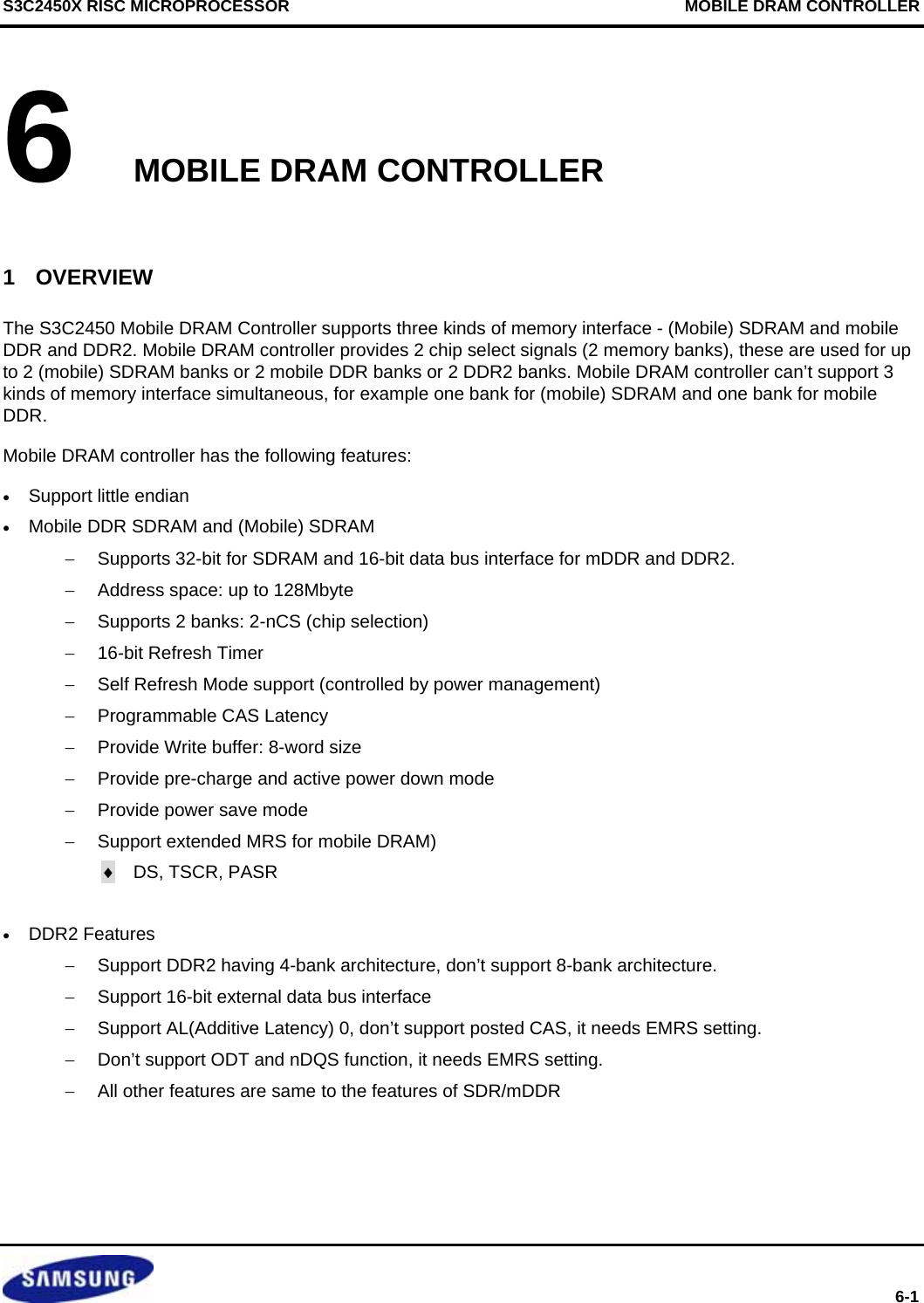
![S3C2450X RISC MICROPROCESSOR MOBILE DRAM CONTROLLER 6-3 3 MOBILE DRAM INITIALIZATION SEQUENCE On power-on reset, software must initialize the memory controller and the mobile DRAM connected to the controller. Refer to the mobile DRAM(SDRAM or mDDR or DDR2) data sheet for the start up procedure, and example sequences are given below: 3.1 MOBILE DRAM(SDRAM OR MOBILE DDR) INITIALIZATION SEQUENCE 1. Wait 200us to allow DRAM power and clock stabilize. 2. Setting the Configuration Register0. This is for MRS and EMRS command to DRAM. 3. Program the configuration register1, and 3 to their normal operation values 4. Program the INIT[1:0] to ‘01b’. This automatically issues a PALL(pre-charge all) cammand to the DRAM. 5. Write ‘0xff’ into the refresh timer register. This provides a refresh cycle every 255-clock cycles. 6. Wait minimum 2 auto-refresh cycle; DRAM requires minimun 2 auto-refresh cycle. 7. Program the INIT[1:0] of Control Register1 to ‘10b’. This automatically issues a MRS command to the DRAM 8. Program the normal operational value(auto-refresh ducy cycle) into the refresh timer. 9. Program the INIT[1:0] of Control Register1 to ‘11b’. This automatically issues a EMRS command to the Mobile DRAM, It’s only needed for Mobile DRAM. 10. Program the INIT[1:0] to ‘00b’. The controller enters the normal mode. 11. The external DRAM is now ready for normal operation. 3.2 DDR2 INITIALIZATION SEQUENCE 1. Setting the BANKCFG & BANKCON1, 2, 3 2. Wait 200us to allow DRAM power and clock stabilize. 3. Wait minimum of 400 ns then issue a PALL(pre-charge all) command. Program the INIT[1:0] to ‘01b’. This automatically issues a PALL(pre-charge all) cammand to the DRAM. 4. Issue an EMRS command to EMR(2), provide LOW to BA0, High to BA1. Program the INIT[1:0] of Control Register1 to ‘11b’ & BANKCON3[31]=’1b’ 5. Issue an EMRS command to EMR(3), provide High to BA0 and BA1. Program the INIT[1:0] of Control Register1 to ‘11b’ & BANKCON3[31:30]=’11b’ 6. Issue an EMRS to enable DLL and RDQS, nDQS, ODT disable. 7. Issue a Mode Register Set command for DLL reset.(To issue DLL Reset command, provide HIGH to A8 and LOW to BA0-BA1, and A13-A15.) Program the INIT[1:0] to ‘10b’. & BANKCON3[8]=’1b’ 8. Issue a PALL(pre-charge all) command. Program the INIT[1:0] to ‘01b’. This automatically issues a PALL(pre-charge all) cammand to the DRAM. 9. Issue 2 or more auto-refresh commands. 10. Issue a MRS command with LOW to A8 to initialize device operation. Program the INIT[1:0] to ‘10b’. & BANKCON3[8]=’0b’ 11. Wait 200 clock after step 7, execute OCD Calibration. 12. The external DRAM is now ready for normal operation](https://usermanual.wiki/Diasonic-Technology-Co/RVM-704M.Users-Manual/User-Guide-1826140-Page-161.png)
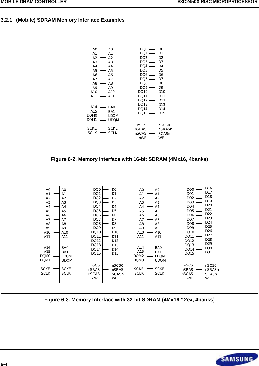
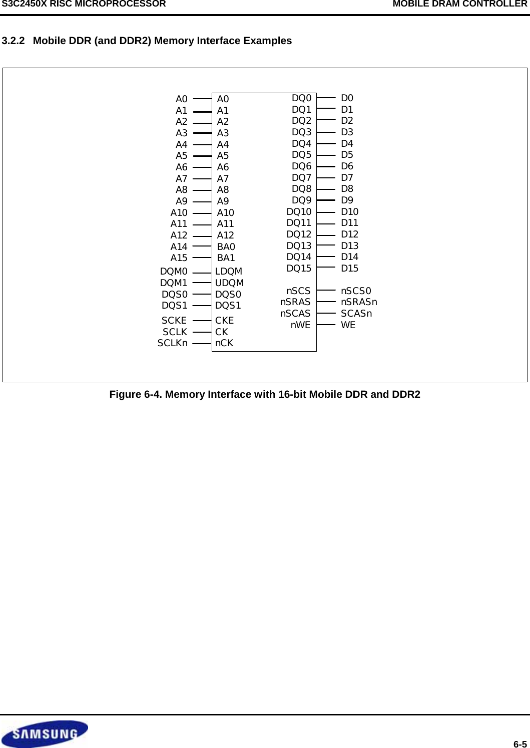
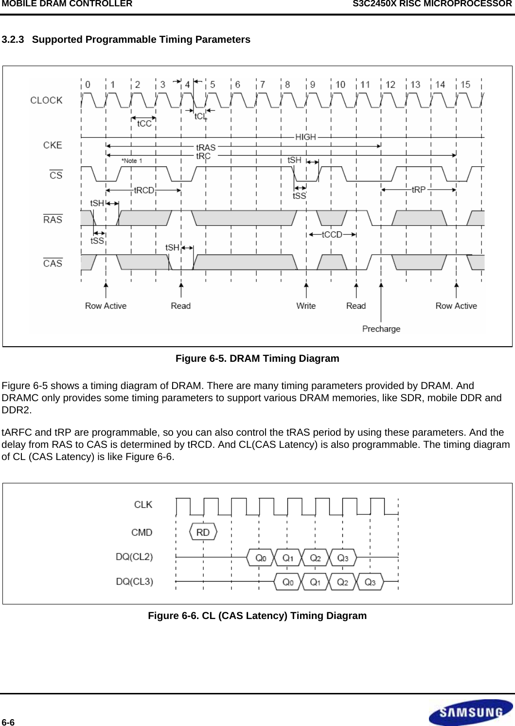
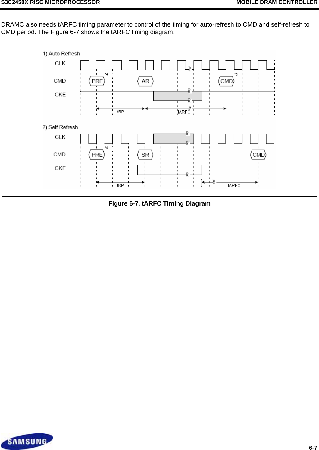
![MOBILE DRAM CONTROLLER S3C2450X RISC MICROPROCESSOR 6-8 3.3 MOBILE DRAM CONFIGURATION REGISTER Register Address R/W Description Reset Value BANKCFG 0x48000000 R/W Mobile DRAM configuration register 0x0000_000C BANKCFG Bit Description Initial State Reserved [31:19] Reserved 0x0000 RASBW0 [18:17] The bit width of RAS (row) address of bank 0 00 = 11-bit 01 = 12-bit 10 = 13-bit 11 = 14-bit 00b Reserved [16] Reserved 0b RASBW1 [15:14] The bit width of RAS (row) address of bank 1 00 = 11-bit 01 = 12-bit 10 = 13-bit 11 = 14-bit 00b Reserved [13] Reserved 0b CASBW0 [12:11] The bit width of CAS (column) address of bank 0 00 = 8-bit 01 = 9-bit 10 = 10-bit 11 = 11-bit 00b Reserved [10] Reserved 0b CASBW1 [9:8] The bit width of CAS (column) address of bank 1 00 = 8-bit 01 = 9-bit 10 = 10-bit 11 = 11-bit 00b ADDRCFG0 [7:6] Memory address configuration of 00 = {BA, RAS, CAS} 01 = {RAS, BA, CAS} 0b ADDRCFG1 [5:4] Memory address configuration 00 = {BA, RAS, CAS} 01 = {RAS, BA, CAS} 0b MEMCFG [3:1] 000 = SDR 001 = DDR2 010 = mSDR 110 = mDDR 011 = 100 = 101 = 111 = Reserved 110b BW [0] Determine external memory data bus width 0 = 32-bit 1 = 16-bit 0b](https://usermanual.wiki/Diasonic-Technology-Co/RVM-704M.Users-Manual/User-Guide-1826140-Page-166.png)
![S3C2450X RISC MICROPROCESSOR MOBILE DRAM CONTROLLER 6-9 3.4 MOBILE DRAM CONTROL REGISTER Register Address R/W Description Reset Value BANKCON1 0x48000004 R/W Mobile DRAM control register 0x4400_0040 BANKCON Bit Description Initial State BUSY [31] DRAM controller status bit (read only) 0 = IDLE 1 = BUSY 0b DQSInDLL* [30:28] DQSIn Delay selection Should be set ‘3’ 100b Reserved [27:26] Should be ‘1’ 01b Reserved [25:8] Should be ‘1’ 0 BStop [7] Read Burst stop control 0 = Not support Read Burst Stop 1 = Support Read Burst Stop Note: This function is only valid in mDDR interface. 0b WBUF [6] Write buffer control 0 = Disable 1 = Enable Note: Disabling the write buffer will flush any stored values to the external DRAM memory. 1b AP [5] Auto pre-charge control 0 = Enable auto pre-charge 1 = Disable auto pre-charge Note: If PWRDN is enabled, then AP=0 provides pre-charge power down and AP=1 provides active power down. 0b PWRDN [4] 0 = Not support DRAM power down control 1 = Support DRAM power down control 0b Reserved [3:2] Reserved 00b INIT [1:0] DRAM initialization control 00 = Normal operation 01 = Issue PALL command 10 = Issue MRS command 11 = Issue EMRS command 00b](https://usermanual.wiki/Diasonic-Technology-Co/RVM-704M.Users-Manual/User-Guide-1826140-Page-167.png)
![MOBILE DRAM CONTROLLER S3C2450X RISC MICROPROCESSOR 6-10 3.5 MOBILE DRAM TIMMING CONTROL REGISTER Register Address R/W Description Reset Value BANKCON2 0x48000008 R/W Mobile DRAM timing control register 0x0099_003F TIMECON Bit Description Initial State Reserved [31:24] Reserved 0x00 tRAS [23:20] Row active time 0000 = 1-clock 0001 = 2-clock 0010 = 3-clock 0011 = 4-clock 0100 = 5-clock 0101 = 6-clock 0110 = 7-clock 0111 = 8-clock 1000 = 9-clock 1001 = 10-clock 1010 = 11-clock 1011 = 12-clock 1100 = 13-clock 1101 = 14-clock 1110 = 15-clock 1111 = 16-clock 1001b tARFC [19:16] Self-refresh or Auto-refresh to next command cycle time 0000 = 1-clock 0001 = 2-clock 0010 = 3-clock 0011 = 4-clock 0100 = 5-clock 0101 = 6-clock 0110 = 7-clock 0111 = 8-clock 1000 = 9-clock 1001 = 10-clock 1010 = 11-clock 1011 = 12-clock 1100 = 13-clock 1101 = 14-clock 1110 = 15-clock 1111 = 16-clock 1001b Reserved [15:6] Reserved 0x000 CAS Latency [5:4] CAS Latency Control 00 = Reserved 01 = 1-clock 10 = 2-clock 11 = 3-clock 011b tRCD [3:2] RAS to CAS delay 00 = 1-clock 01 = 2-clock 10 = 3-clock 11 = 4-clock 11b tRP [1:0] Row pre-charge time 00 = 1-clock 01 = 2-clock 10 = 3-clock 11 = 4-clock 11b](https://usermanual.wiki/Diasonic-Technology-Co/RVM-704M.Users-Manual/User-Guide-1826140-Page-168.png)
![S3C2450X RISC MICROPROCESSOR MOBILE DRAM CONTROLLER 6-11 3.6 MOBILE DRAM (EXTENDED ) MODE REGISTER SET REGISTER Register Address R/W Description Reset Value BANKCON3 0x4800000C R/W Mobile DRAM (E)MRS Register 0x8000_0003 3.6.1 mSDRAM / mDDR PnBANKCON Bit Description Initial State BA [31:30] Bank address for EMRS 10b Reserved [29:23] Should be ‘0’ 0000000b DS [22:21] DS(Driver Strength) for EMRS 00b Reserved [20:19] Should be ‘0’ 00b PASR [18:16] PASR(Partial Array Self Refresh) for EMRS 000b BA [15:14] Bank address for MRS 0b Reserved [15:7] Should be ‘0’ 000000000b CAS Latency [6:4] CAS Latency for MRS 00 = Reserved 01 = 1-clock 10 = 2-clock 11 = 3-clock 000b Burst Type [3] DRAM Burst Type (Read Only) Only support sequential burst type. 0b Burst Length [2:0] DRAM Burst Length (Read Only) This value is determined internally. 011b NOTE: Bit[15:0] is used for MRS command cycle, and Bit[31:16] is for EMRS command cycle. You can program this register as memory type you are using. Each 16-bit exactly map the (E)MRS register bit location. Refer to memory data sheet.](https://usermanual.wiki/Diasonic-Technology-Co/RVM-704M.Users-Manual/User-Guide-1826140-Page-169.png)
![MOBILE DRAM CONTROLLER S3C2450X RISC MICROPROCESSOR 6-12 3.6.2 DDR2 Memory MRS[15:0] and EMRS(1)[31:16] PnBANKCON Bit Description Initial State BA [31:30] Bank address for EMRS 10b Reserved [29] Should be ‘0’ 0b Qoff [28] 0 = Output buffer enable 1 = Output buffer disable 0b RDQS [27] 0 = Disable 1 = Enable 0b nDQS [26] 0 = Enable 1 = Disable 0b OCD program [25:23] Refer to DDR2 spec. 000b Additive latency [21:19] Refer to DDR2 spec. 000b Rtt [22] [18] 00 = ODT disable 01 = 75Ω 10 = 150Ω 11 = 50Ω 00b D.I.C [17] 0 = Full strength 1 = Reduced strength 0b DLL enable [16] 0 = Enable 1 = Disable 0b Reserved [15:13] Should be ‘0’ 000b Active Power down exit time [12] 0 = Fast exit 1 = Slow exit 0b WR [11:9] Write recovery for auto pre-charge 000b DLL Reset [8] 0 = No 1 = Yes 0b TM [7] 0 = Normal 1 = Test 0b CAS Latency [6:4] CAS Latency for MRS 00 = Reserved 01 = 1-clock 10 = 2-clock 11 = 3-clock 000b Burst Type [3] DRAM Burst Type (Read Only) Only support sequential burst type. 0b Burst Length [2:0] DRAM Burst Length (Read Only) This value is determined internally. 011b](https://usermanual.wiki/Diasonic-Technology-Co/RVM-704M.Users-Manual/User-Guide-1826140-Page-170.png)
![S3C2450X RISC MICROPROCESSOR MOBILE DRAM CONTROLLER 6-13 3.6.3 DDR2 Memory EMRS(2)[31:16] PnBANKCON Bit Description Initial State BA [31:30] Bank address for EMRS 10b Reserved [29:24] Should be ‘0’ 000000b SRF [23] High Temperature Self-Refresh Rate Enable 0 = Disable 1 = Enable 0b Reserved [22:20] Should be ‘0’ 000b DCC [19] 0 = Disable 1 = Enable 0b PASR [18:16] PASR(Partial Array Self Refresh) for EMRS(2) 000b 3.6.4 DDR2 Memory EMRS(3)[31:16] PnBANKCON Bit Description Initial State BA [31:30] Bank address for EMRS 10b Reserved [29:16] Should be ‘0’ 0x0](https://usermanual.wiki/Diasonic-Technology-Co/RVM-704M.Users-Manual/User-Guide-1826140-Page-171.png)
![MOBILE DRAM CONTROLLER S3C2450X RISC MICROPROCESSOR 6-14 3.7 MOBILE DRAM REFRESH CONTROL REGISTER Register Address R/W Description Reset Value REFRESH 0x48000010 R/W Mobile DRAM refresh control register 0x0000_0020 REFRESH Bit Description Initial State Reserved [31:16] Reserved 0x0000 REFCYC [15:0] DRAM refresh cycle. Example: Refresh period is 15.6us, and HCLK is 66MHz. The value of REFCYC is as follows: REFCYC = 15.6 x 10-6 x 66 x 106 = 1029 0x0020 3.8 MOBILE DRAM WRITE BUFFER TIME OUT REGISTER A write to a enabling write buffer loads the value in the timeout register into timeout down counter of the buffer. When the timeout counter reached 0 the contents of write buffer is flushed to the external DRAM. The down counter is clocked HCLK. Writing a value of 0 in the TIMEOUT register disables the write buffer timeout function. Register Address R/W Description Reset ValueTIMEOUT 0x48000014 R/W Write Buffer Time out control register 0x0000_0000 TIMEOUT Bit Description Initial StateReserved [31:16] Reserved 0x0000 TIMEOUT [15:0] Write buffer time-out delay time 0x0000](https://usermanual.wiki/Diasonic-Technology-Co/RVM-704M.Users-Manual/User-Guide-1826140-Page-172.png)
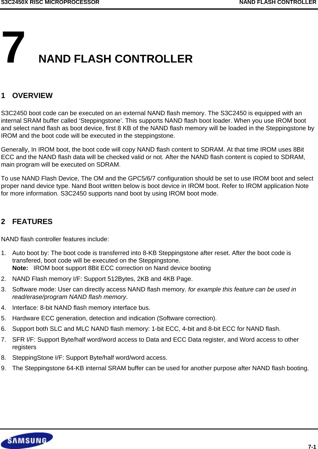
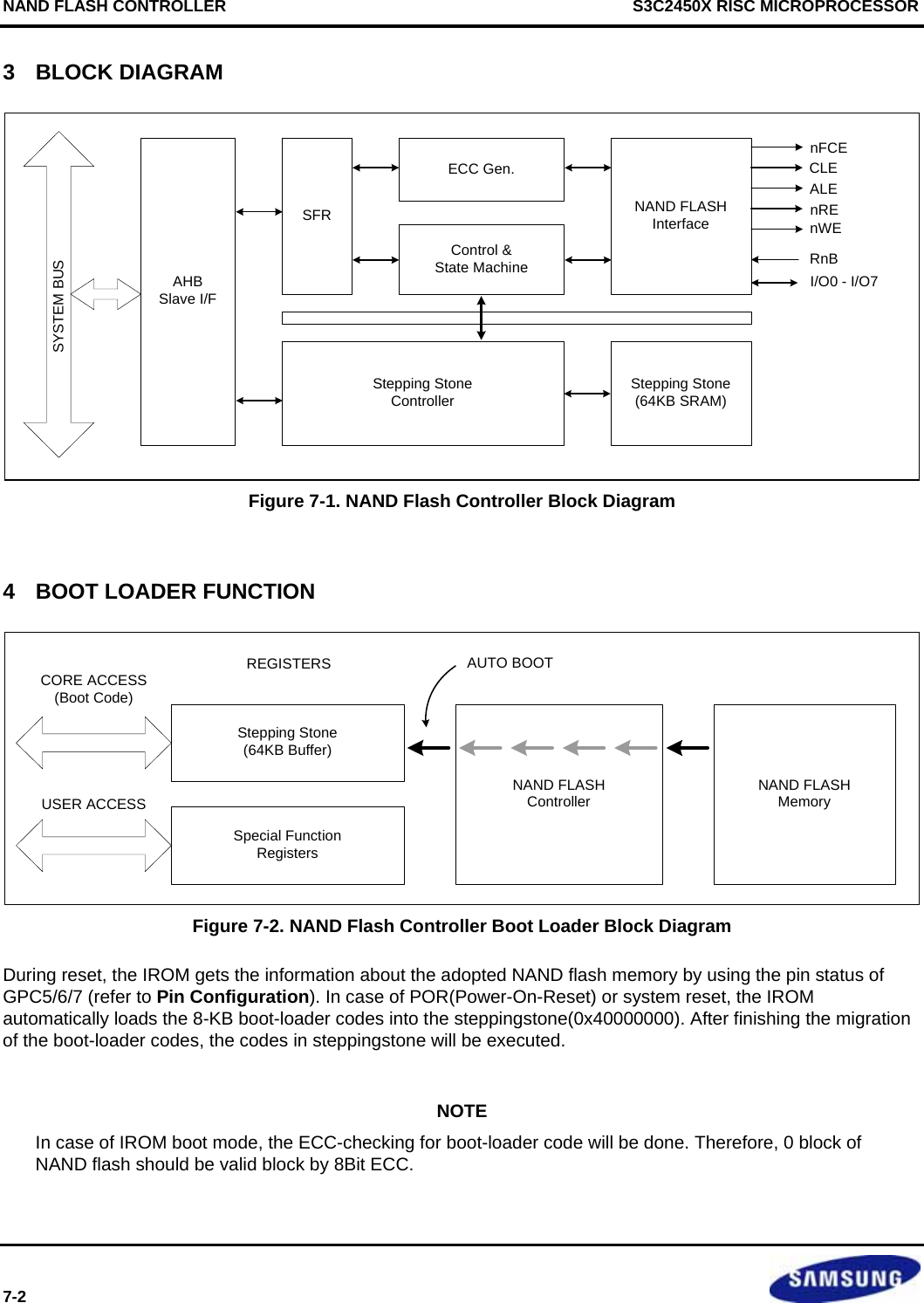
![S3C2450X RISC MICROPROCESSOR NAND FLASH CONTROLLER 7-3 5 GPC5/6/7 PIN CONFIGURATION TABLE IN IROM BOOT MODE Page Address Cycle GPC7 [2] GPC6 [1] GPC5 [0] MMC(MoviNAND/iNand) - - 0 0 0 Reserved - - 0 0 1 3 0 1 0 512 4 0 1 1 4 1 0 0 2048 5 1 0 1 Nand 4096 5 1 1 0 Above configuration is applicable when NAND Flash is used as booting memory in IROM boot mode. If NAND Flash is not used as boot memory, the configuration can be changed by setting NFCON SFR ’NFCONF’ (0x4E000000). PageSize, PageSize_Ext and AddrCycle are fields in NFCONF(0x4E000000). 6 NAND FLASH MEMORY TIMING HCLKCLE / ALEnWETACLS TWRPH0 TWRPH1DATA COMMAND / ADDRESS Figure 7-3. CLE & ALE Timing (TACLS=1, TWRPH0=0, TWRPH1=0) Block Diagram](https://usermanual.wiki/Diasonic-Technology-Co/RVM-704M.Users-Manual/User-Guide-1826140-Page-175.png)
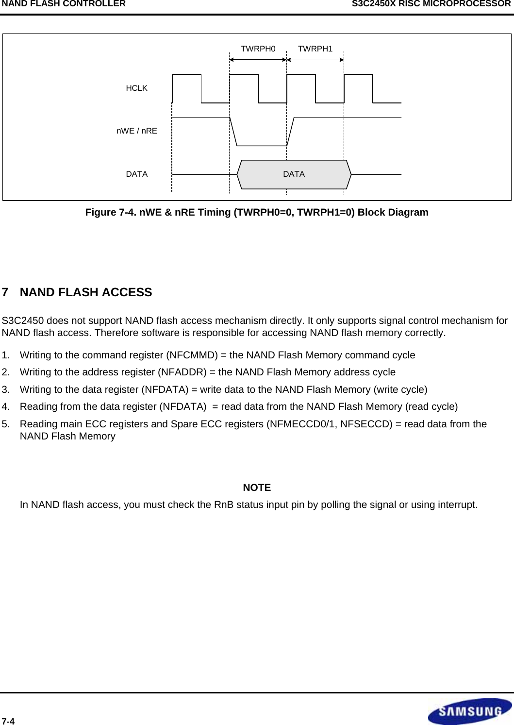
![S3C2450X RISC MICROPROCESSOR NAND FLASH CONTROLLER 7-5 8 DATA REGISTER CONFIGURATION 8.1.1 8-bit NAND Flash Memory Interface A. Word Access Register Bit [31:24] Bit [23:16] Bit [15:8] Bit [7:0] NFDATA 4th I/O[ 7:0] 3rd I/O[ 7:0] 2nd I/O[ 7:0] 1st I/O[ 7:0] B. Half-word Access Register Bit [31:24] Bit [23:16] Bit [15:8] Bit [7:0] NFDATA Invalid value Invalid value 2nd I/O[ 7:0] 1st I/O[ 7:0] C. Byte Access Register Bit [31:24] Bit [23:16] Bit [15:8] Bit [7:0] NFDATA Invalid value Invalid value Invalid value 1st I/O[ 7:0] 9 STEPPINGSTONE (8KB IN 64KB SRAM) The NAND Flash controller uses Steppingstone as the buffer on booting and also you can use this area for various other purpose. 10 1BIT / 4BIT / 8BIT ECC (ERROR CORRECTION CODE) NAND flash controller has four ECC (Error Correction Code) modules for 1 bit ECC, one for 4bit ECC and one for 8bit ECC. The 1bit ECC modules for main data area can be used for (up to) 2048 bytes ECC parity code generation, and 1 bit ECC module for spare area can be used for (up to) 4 bytes ECC Parity code generation. Both 4bit and 8bit ECC modules can be used for only 512 bytes ECC parity code generation. 4 bit and 8bit ECC modules generate the parity codes for each 512 byte. However, 1 bit ECC modules generate parity code per byte lane separately. 10.1 ECC MODULE FEATURES ECC generation is controlled by the ECC Lock (MainECCLock, SpareECCLock) bit of the Control register. When ECCLock is Low, ECC codes are generated by the H/W ECC modules.](https://usermanual.wiki/Diasonic-Technology-Co/RVM-704M.Users-Manual/User-Guide-1826140-Page-177.png)
![NAND FLASH CONTROLLER S3C2450X RISC MICROPROCESSOR 7-6 10.1.1 1-BIT ECC Register Configuration Following tables shows the configuration of 1-bit ECC value read from spare area of external NAND flash memory. For comparing to ECC parity code generated by the H/W modules, each ECC data read from memory must be written to NFMECCDn for main area and NFSECCD for spare area. NOTE 4-bit ECC decoding scheme is different to 1-bit ECC. 1. NAND Flash Memory Interface Register Bit [31:24] Bit [23:16] Bit [15:8] Bit [7:0] NFMECCD0 Not used 2nd ECC for I/O[7:0] Not used 1st ECC for I/O[7:0] NFMECCD1 Not used 4th ECC for I/O[7:0] Not used 3rd ECC for I/O[7:0] Register Bit [31:24] Bit [23:16] Bit [15:8] Bit [7:0] NFSECCD Not used 2nd ECC for I/O[7:0] Not used 1st ECC for I/O[7:0]](https://usermanual.wiki/Diasonic-Technology-Co/RVM-704M.Users-Manual/User-Guide-1826140-Page-178.png)
![S3C2450X RISC MICROPROCESSOR NAND FLASH CONTROLLER 7-7 10.2 1-BIT ECC PROGRAMMING ENCODING AND DECODING 1. To use 1-bit ECC in software mode, reset the ECCType to ‘0’ (enable 1-bit ECC)‘. ECC module generates ECC parity code for all read / write data when MainECCLock (NFCONT[7]) and SpareECCLock (NFCONT[6]) are unlocked(‘0’). You must reset ECC value by writing the InitMECC (NFCONT[5]) and InitSECC (NFCONT[4]) bit as ‘1’ and have to clear the MainECCLock (NFCONT[7]) bit to ‘0’(Unlock) before read or write data. MainECCLock (NFCONT[7]) and SpareECCLock(NFCONT[6]) bit controls whether ECC Parity code is generated or not. 2. Whenever data is read or written, the ECC module generates ECC parity code on register NFMECC0/1. 3. After you complete read or write one page (does not include spare area data), Set the MainECCLock bit to ‘1’ (Lock). ECC Parity code is locked and the value of the ECC status register will not be changed. 4. To generate spare area ECC parity code, Clear SpareECCLock (NFCONT[6]) bit to ‘0’ (unlock). 5. Whenever data is read or written, the spare area ECC module generates ECC parity code on register NFSECC. 6. After you complete read or write spare area, set the SpareECCLock bit to '1' (Lock). ECC Parity code is locked and the value of the ECC status register will not be changed. 7. From now on, you can use these values to record to the spare area or check the bit error. 8. For example, to check the bit error of main data area on page read operation, after generating of ECC codes for main data area, you have to move the ECC parity codes (is stored to spare area) to NFMECCD0 and NFMECCD1. From this time, the NFECCERR0 have the valid error status values. NOTE NFSECCD is for the ECC value in spare area. Usually, the user will write the ECC value generated from main data area to Spare area, which value will be the same as NFMECC0/1. 10.3 4-BIT ECC PROGRAMMING GUIDE (ENCODING) 1. To use 4-bit ECC in software mode, set the MsgLength to 0(512-byte message length) and set the ECCType to ‘1’(enable 4-bit ECC). ECC module generates ECC parity code for 512-byte write data. So, you have to reset ECC value by writing the InitMECC (NFCONT[5]) bit as ‘1’ and have to clear the MainECCLock (NFCONT[7]) bit to ‘0’(Unlock) before write data. MainECCLock (NFCONT[7]) bit controls whether ECC Parity code is generated or not. 2. Whenever data is written, the 4-bit ECC module generates ECC parity code internally. 3. After you finish writing 512-byte data (not include spare area data), the parity codes are automatically updated to NFMECC0, NFMECC1 register. If you use 512-byte NAND flash memory, you can program these values to spare area. However, if you use NAND flash memory more than 512-byte page, you can’t program immediately. In this case, you have to copy these parity codes to other memory like DRAM. After writing all main data, you can write the copied ECC values to spare area. The parity codes have self-correctable information include parity code itself. 4. To generate spare area ECC parity code, set the MsgLength to 1(24-byte message length), and set the ECCType to '1'(enable 4-bit ECC). ECC module generates ECC parity code for 24-byte write data. So you have to reset ECC value by writing the InitMECC (NFCONT[5]) bit as '1' and have to clear the MainECCLock (NFCONT[7]) bit to ‘0’(Unlock) before write data. MainECCLock (NFCONT[7]) bit controls whether ECC Parity code is generated or not. 5. Whenever data is written, the 4-bit ECC module generates ECC parity code internally. 6. When you finish writing 24-byte meta or extra data, the parity codes are automatically updated to NFMECC0, NFMECC1 register. You can program these parity codes to spare area. The parity codes have self-correctable information include parity code itself.](https://usermanual.wiki/Diasonic-Technology-Co/RVM-704M.Users-Manual/User-Guide-1826140-Page-179.png)
![NAND FLASH CONTROLLER S3C2450X RISC MICROPROCESSOR 7-8 10.4 4-BIT ECC PROGRAMMING GUIDE (DECODING) 1. To use 4-bit ECC, set the MsgLength to 0(512-byte message length) and set the ECCType to ‘1’(enable 4-bit ECC). ECC module generates ECC parity code for 512-byte read data. So, you have to reset ECC value by writing the InitMECC (NFCONT[5]) bit as ‘1’ and have to clear the MainECCLock (NFCONT[7]) bit to ‘0’(Unlock) before read data. MainECCLock (NFCONT[7]) bit controls whether ECC Parity code is generated or not. 2. Whenever data is read, the 4-bit ECC module generates ECC parity code internally. 3. After you complete read 512-byte (does not include spare area data), you have to read parity codes. 4-bit ECC module needs parity codes to detect whether error bits are or not. So you have to read ECC parity code right after read 512-byte. Once ECC parity code is read, 4-bit ECC engine start to search any error internally. 4-bit ECC error searching engine need minimum 155 cycles to find any error. During this time, you can continue read main data from external NAND flash memory. ECCDecDone(NFSTAT[6]) can be used to check whether ECC decoding is completed or not. 4. When ECCDecDone (NFSTAT[6]) is set (‘1’), NFECCERR0 indicates whether error bit exist or not. If any error exists, you can fix it by referencing NFECCERR0/1 and NFMLCBITPT register. 5. If you have more main data to read, continue to step 2. 6. For meta data error check, set the MsgLength to 1(24-byte message length) and set the ECCType to ‘1’(enable 4-bit ECC). ECC module generates ECC parity code for 24-byte read data. So you have to reset ECC value by writing the InitMECC (NFCONT[5]) bit as ‘1’ and have to clear the MainECCLock (NFCONT[7]) bit to ‘0’(Unlock) before read data. MainECCLock (NFCONT[7]) bit controls whether ECC Parity code is generated or not. 7. Whenever data is read, the 4-bit ECC module generates ECC parity code internally. 8. After you complete read 24-byte, you have to read parity codes. 4-bit ECC module needs parity codes to detect whether error bits are or not. So you have to read ECC parity codes right after read 24-byte. Once ECC parity code is read, 4-bit ECC engine start to search any error internally. 4-bit ECC error searching engine need minimum 155 cycles to find any error. During this time, you can continue read main data from external NAND flash memory. ECCDecDone(NFSTAT[6]) can be used to check whether ECC decoding is completed or not. 9. When ECCDecDone (NFSTAT[6]) is set (‘1’), NFECCERR0 indicates whether error bit exist or not. If any error exists, you can fix it by referencing NFECCERR0/1 and NFMLCBITPT register. 10.5 8-BIT ECC PROGRAMMING GUIDE (ENCODING) 1. To use 8-bit ECC in software mode, set the MsgLength to 0(512-byte message length) and set the ECCType to “01”(enable 8-bit ECC). ECC module generates ECC parity code for 512-byte write data. In order to start the ECC module, you have to write ‘1’ on the InitMECC (NFCONT[5]) bit after cleaning the MainECCLock (NFCONT[7]) bit to ‘0’ (Unlock). MainECCLock (NFCONT[7]) bit controls whether ECC Parity code is generated or not. NOTE: In 8bit ECC, MainECCLock should be cleared before initiating InitMECC. 2. Whenever data is written, the 8bit ECC module generates ECC parity code internally. 3. After you finish writing 512-byte data (not include spare area data), the parity codes are automatically updated to NF8MECC0, NFMECC1, NF8MECC2, NF8MECC3 register. If you use 512-byte NAND flash memory, you can program these values directly to spare area. However, if you use NAND flash memory more than 512-byte page, you can’t program immediately. In this case, you have to copy these parity codes to other memory like DRAM. After writing all main data, you can write the copied ECC values to spare area. The parity codes have self-correctable information include parity code itself.](https://usermanual.wiki/Diasonic-Technology-Co/RVM-704M.Users-Manual/User-Guide-1826140-Page-180.png)
![S3C2450X RISC MICROPROCESSOR NAND FLASH CONTROLLER 7-9 4. To generate spare area ECC parity code, set the MsgLength to 1(24-byte message length), and set the ECCType to “01”(enable 8bit ECC). 8bit ECC module generates the ECC parity code for 24-byte data. In order to initiating the module, you have to write ‘1’ on the InitMECC (NFCONT[5]) bit after clearing the MainECCLock (NFCONT[7]) bit to ‘0’(Unlock). MainECCLock (NFCONT[7]) bit controls whether ECC Parity code is generated or not. NOTE: In 8bit ECC, MainECCLock should be cleared before initiating InitMECC. 5. Whenever data is written, the 8bit ECC module generates ECC parity code internally. 6. When you finish writing 24-byte meta or extra data, the parity codes are automatically updated to NF8MECC0, NFMECC1, NF8MECC2, NF8MECC3 register. You can program these parity codes to spare area. The parity codes have self-correctable information include parity code itself. 10.6 8-BIT ECC PROGRAMMING GUIDE (DECODING) 1. To use 8bit ECC in software mode, set the MsgLength to 0(512-byte message length) and set the ECCType to “01”(enable 8bit ECC). 8bit ECC module generates ECC parity code for 512-byte read data. In order to initiating 8bit ECC module, you have to write ‘1’ on the InitMECC (NFCONT[5]) bit after clearing the MainECCLock (NFCONT[7]) bit to ‘0’(Unlock). MainECCLock (NFCONT[7]) bit controls whether ECC Parity code is generated or not. NOTE: In 8bit ECC, MainECCLock should be cleared before InitMECC 2. Whenever data is read, the MLC ECC module generates ECC parity code internally. 3. After you complete the reading of 512-byte data (not including spare area data), you must set the MainECCLock (NFCONT[7]) bit to ‘1’(Lock) and have to read parity codes. 8bit ECC module needs parity codes to detect whether error bits exists or not. So you have to read the ECC parity code of 512-byte main data right after reading the 512-byte data. Once the ECC parity code is read, 8bit ECC engine starts searching any error internally. 8bit ECC error searching engine needs minimum 372 cycles to find any error. During this time, you can continue reading data from external NAND flash memory. ECCDecDone(NFSTAT[6]) can be used to check whether ECC decoding is completed or not. 4. When ECCDecDone (NFSTAT[6]) is set (‘1’), NF8ECCERR0 indicates whether error bit exists or not. If any error exists, you can fix it by referencing NF8ECCERR0/1/2 and NFMLC8BITPT0/1 register. 5. If you have more main data to read, continue doing from step 1. 6. For meta data error check, set the MsgLength to 1(24-byte message length) and set the ECCType to “01”(enable 8bit ECC). ECC module generates the ECC parity code for 24-byte data. In order to initiating the 8bit ECC module, you have to write ‘1’ on the InitMECC (NFCONT[5]) bit after clearing the MainECCLock (NFCONT[7]) bit to ‘0’(Unlock). MainECCLock (NFCONT[7]) bit controls whether ECC Parity code is generated or not. 7. Whenever data is read, the 8bit ECC module generates ECC parity code internally. 8. After you complete reading 24-byte, you must set the MainECCLock (NFCONT[7]) bit to ‘1’(Lock) and read the parity code for 24-byte data. MLC ECC module needs parity codes to detect whether error bits exists or not. So you have to read ECC parity codes right after reading 24-byte data. Once ECC parity code is read, 8bit ECC engine starts searching any error internally. 8bit ECC error searching engine needs minimum 372 cycles to find any error. During this time, you can continue reading main data from external NAND flash memory. ECCDecDone(NFSTAT[6]) can be used to check whether ECC decoding is completed or not. 9. When ECCDecDone (NFSTAT[6]) is set (‘1’), NF8ECCERR0 indicates whether error bit exist or not. If any error exists, you can fix it by referencing NF8ECCERR0/1/2 and NF8MLCBITPT register.](https://usermanual.wiki/Diasonic-Technology-Co/RVM-704M.Users-Manual/User-Guide-1826140-Page-181.png)
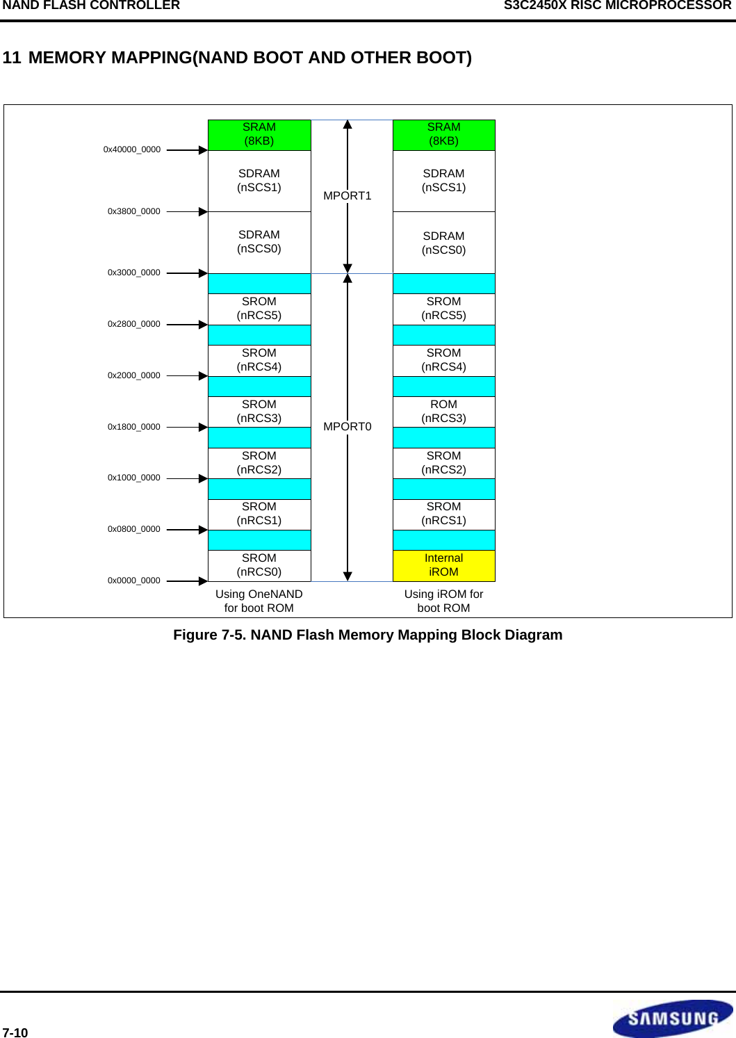
![S3C2450X RISC MICROPROCESSOR NAND FLASH CONTROLLER 7-11 12 NAND FLASH MEMORY CONFIGURATION Figure 7-6. A 8-bit NAND Flash Memory Interface Block Diagram NOTE: NAND CONTROLLER can support to control two nand flash memories . NAND CS Other BOOT nFCE NAND CONTROLLER CS0 Configurable nRCS[1] NAND CONTROLLER CS1 Configurable If you want NAND BOOT by IROM, nFCE must be used to boot.](https://usermanual.wiki/Diasonic-Technology-Co/RVM-704M.Users-Manual/User-Guide-1826140-Page-183.png)
![S3C2450X RISC MICROPROCESSOR NAND FLASH CONTROLLER 7-13 13.2 NAND FLASH CONFIGURATION REGISTER Register Address R/W Description Reset ValueNFCONF 0x4E000000 R/W NAND Flash Configuration register 0xX000100X NFCONF Bit Description Initial State Reserved [31] Reserved 0 Reserved [30] Should be 0 0 Reserved [29:26] Reserved 0000 MsgLength [25] Message (Data) length for 4/8 bit ECC 0 = 512-byte 1 = 24-byte 0 ECCType [24:23] This bit indicates what kind of ECC should be used. 00 = 1-bit ECC 10 = 4-bit ECC 01 = 8-bit ECC Note: Don’t confuse the value of 4-bit ECC and 8-bit ECC. H/W Set (CfgBootEcc) Reserved [22:15] Reserved 000000000 TACLS [14:12] CLE & ALE duration setting value (0~7) Duration = HCLK x TACLS 001 Reserved [11] Reserved 0 TWRPH0 [10:8] TWRPH0 duration setting value (0~7) Duration = HCLK x ( TWRPH0 + 1 ) 000 Reserved [7] Reserved 0 TWRPH1 [6:4] TWRPH1 duration setting value (0~7) Duration = HCLK x ( TWRPH1 + 1 ) 000 PageSize [3] This bit indicates the page size of NAND Flash Memory When PageSize_Ext is 1, the value of PageSize means following: 0 = 512 Bytes/page, 1 = 2048 Bytes/page When PageSize_Ext is 0, the value of PageSize means following: 0 = 2048 Bytes/page, 1 = 4096 Bytes/page H/W Set (CfgAdvFlash) PageSize_Ext [2] This bit indicated what kind of NAND Flash memory is used. 0 = Large Size NAND Flash 1 = Small Size NAND Flash This bit is determined by OM[2] pin status on reset and wake-up time from sleep mode. This bit can be changed by software later. 1](https://usermanual.wiki/Diasonic-Technology-Co/RVM-704M.Users-Manual/User-Guide-1826140-Page-185.png)
![NAND FLASH CONTROLLER S3C2450X RISC MICROPROCESSOR 7-14 NFCONF Bit Description Initial State AddrCycle [1] This bit indicates the number of Address cycle of NAND Flash memory. When Page Size is 512 Bytes, 0 = 3 address cycle 1 = 4 address cycle When page size is 2K or 4K, 0 = 4 address cycle 1 = 5 address cycle This bit is determined by OM[1] pin on reset and wake-up time from sleep mode. This bit can be changed by software later. H/W Set (CfgAddrCycle) BusWidth [0] This bit indicates the I/O bus width of NAND Flash Memory. The value of BusWidth means the followings. 0 = 8-bit bus This bit has no meaning in NAND-boot by IROM, when the I/O bus width is only 8-bit. BusWidth has effects on normal access.. This bit should be 0 H/W Set (CfgBusWidth)](https://usermanual.wiki/Diasonic-Technology-Co/RVM-704M.Users-Manual/User-Guide-1826140-Page-186.png)
![S3C2450X RISC MICROPROCESSOR NAND FLASH CONTROLLER 7-15 13.3 CONTROL REGISTER Register Address R/W Description Reset ValueNFCONT 0x4E000004 R/W NAND Flash control register 0x000100C6 NFCONT Bit Description Initial StateReserved [31:19] Reserved 0 ECC Direction [18] 4-bit, 8-bitECC encoding / decoding control 0 = Decoding 4-bit, 8bit ECC, It is used for page read 1 = Encoding 4-bit, 8-bit ECC, It is be used for page program 0 Lock-tight [17] Lock-tight configuration 0 = Disable lock-tight 1 = Enable lock-tight, Once this bit is set to 1, you cannot clear. Only reset or wake up from sleep mode can make this bit disable (cannot cleared by software). When it is set to 1, the area setting in NFSBLK (0x4E000020) to NFEBLK (0x4E000024) is unlocked, and except this area, write or erase command will be invalid and only read command is valid. When you try to write or erase locked area, the illegal access will be occurred (NFSTAT [5] bit will be set). If the NFSBLK and NFEBLK are same, entire area will be locked. 0 Soft Lock [16] Soft Lock configuration 0 = Disable lock 1 = Enable lock Soft lock area can be modified at any time by software. When it is set to 1, the area setting in NFSBLK (0x4E000020) to NFEBLK (0x4E000024) is unlocked, and except this area, write or erase command will be invalid and only read command is valid. When you try to write or erase locked area, the illegal access will be occurred (NFSTAT [5] bit will be set). If the NFSBLK and NFEBLK are same, entire area will be locked. 1 Reserved [15:13] Reserved. Should be written to 0. 000 EnbECCDecINT [12] 4-bit, 8-bit ECC decoding completion interrupt control 0 = Disable interrupt 1 = Enable interrupt 0 8bit Stop [11] 8-bit ECC encoding/decoding operation initialization 0](https://usermanual.wiki/Diasonic-Technology-Co/RVM-704M.Users-Manual/User-Guide-1826140-Page-187.png)
![NAND FLASH CONTROLLER S3C2450X RISC MICROPROCESSOR 7-16 NFCONT Bit Description Initial StateEnbIllegalAccINT [10] Illegal access interrupt control 0 = Disable interrupt 1 = Enable interrupt Illegal access interrupt will occurs when CPU tries to program or erase locking area (the area setting in NFSBLK (0x4E000020) to NFEBLK (0x4E000024)). 0 EnbRnBINT [9] RnB status input signal transition interrupt control 0 = Disable RnB interrupt 1 = Enable RnB interrupt 0 RnB_TransMode [8] RnB transition detection configuration 0 = Detect rising edge 1 = Detect falling edge 0 MainECCLock [7] Lock Main area ECC generation 0 = Unlock Main area ECC 1 = Lock Main area ECC Main area ECC status register is NFMECC0/1(0x4E000034/38), 1 SpareECCLock [6] Lock Spare area ECC generation. 0 = Unlock Spare ECC 1 = Lock Spare ECC Spare area ECC status register is NFSECC(0x4E00003C), 1 InitMECC [5] 1 = Initialize main area ECC decoder/encoder (write-only) 0 InitSECC [4] 1 = Initialize spare area ECC decoder/encoder (write-only) 0 Reserved [3] Reserved 0 Reg_nCE1 [2] NAND Flash Memory nRCS[1] signal control 0 = Force nRCS[1] to low(Enable chip select) 1 = Force nRCS[1] to High(Disable chip select) Note: Even Reg_nCE1 and Reg_nCE0 are set to zero simultaneously, only one of them is asserted. 1 Reg_nCE0 [1] NAND Flash Memory nFCE signal control 0 = Force nFCE to low(Enable chip select) 1 = Force nFCE to High(Disable chip select) Note: During boot time, it is controlled automatically. This value is only valid while MODE bit is 1 1 MODE [0] NAND Flash controller operating mode 0 = NAND Flash Controller Disable (Don’t work) 1 = NAND Flash Controller Enable 0](https://usermanual.wiki/Diasonic-Technology-Co/RVM-704M.Users-Manual/User-Guide-1826140-Page-188.png)
![S3C2450X RISC MICROPROCESSOR NAND FLASH CONTROLLER 7-17 13.4 COMMAND REGISTER Register Address R/W Description Reset ValueNFCMMD 0x4E000008 R/W NAND Flash command set register 0x00 NFCMMD Bit Description Initial StateReserved [31:8] Reserved 0x00 NFCMMD [7:0] NAND Flash memory command value 0x00 13.5 ADDRESS REGISTER Register Address R/W Description Reset ValueNFADDR 0x4E00000C R/W NAND Flash address set register 0x0000XX00 REG_ADDR Bit Description Initial StateReserved [31:8] Reserved 0x00 NFADDR [7:0] NAND Flash memory address value 0x00 13.6 DATA REGISTER Register Address R/W Description Reset ValueNFDATA 0x4E000010 R/W NAND Flash data register 0xXXXX NFDATA Bit Description Initial StateNFDATA [31:0] NAND Flash read/program data value for I/O Note: Refer to Data Register Configuration. 0xXXXX](https://usermanual.wiki/Diasonic-Technology-Co/RVM-704M.Users-Manual/User-Guide-1826140-Page-189.png)
![NAND FLASH CONTROLLER S3C2450X RISC MICROPROCESSOR 7-18 13.7 MAIN DATA AREA ECC REGISTER Register Address R/W Description Reset ValueNFMECCD0 0x4E000014 R/W NAND Flash ECC 1st 2nd register for main area data read Note: Refer to ECC Module Features. 0x00000000NFMECCD1 0x4E000018 R/W NAND Flash ECC 3rd 4th register for main area data read Note: Refer to ECC Module Features. 0x00000000 NFMECCD0 Bit Description Initial StateReserved [31:24] Not used 0x00 ECCData1 [23:16] ECC1 for I/O[7:0] 0x00 Reserved [15:8] Not used 0x00 ECCData0 [7:0] ECC0 for I/O[7:0] 0x00 NOTE: Only word access is valid. NFMECCD1 Bit Description Initial StateReserved [31:24] Not used 0x00 ECCData3 [23:16] ECC3 for I/O[7:0] 0x00 Reserved [15:8] Not used 0x00 ECCData2 [7:0] ECC2 for I/O[7:0] 0x00 13.8 SPARE AREA ECC REGISTER Register Address R/W Description Reset ValueNFSECCD 0x4E00001C R/W NAND Flash ECC(Error Correction Code) register for spare area data read 0x00000000 NFSECCD Bit Description Initial StateReserved [31:24] Not used 0x00 SECCData1 [23:16] 2nd Spare area ECC for I/O[7:0] 0x00 Reserved [15:8] Not used 0x00 SECCData0 [7:0] 1st Spare area ECC for I/O[ 7:0] 0x00 NOTE: Only word or half word access is valid.](https://usermanual.wiki/Diasonic-Technology-Co/RVM-704M.Users-Manual/User-Guide-1826140-Page-190.png)
![S3C2450X RISC MICROPROCESSOR NAND FLASH CONTROLLER 7-19 13.9 PROGRMMABLE BLOCK ADDRESS REGISTER Register Address R/W Description Reset ValueNFSBLK 0x4E000020 R/W NAND Flash programmable start block address 0x000000 NFEBLK 0x4E000024 R/W NAND Flash programmable end block address Nand Flash can be programmed between start and end address. When the Soft lock or Lock-tight is enabled and the Start and End address has same value, Entire area of NAND flash will be locked. 0x000000 NFSBLK Bit Description Initial StateReserved [31:24] Reserved 0x00 SBLK_ADDR2 [23:16] The 3rd block address of the block erase operation 0x00 SBLK_ADDR1 [15:8] The 2nd block address of the block erase operation 0x00 SBLK_ADDR0 [7:0] The 1st block address of the block erase operation (Only bit [7:5] are valid) 0x00 NFEBLK Bit Description Initial StateReserved [31:24] Reserved 0x00 EBLK_ADDR2 [23:16] The 3rd block address of the block erase operation 0x00 EBLK_ADDR1 [15:8] The 2nd block address of the block erase operation 0x00 EBLK_ADDR0 [7:0] The 1st block address of the block erase operation (Only bit [7:5] are valid) 0x00](https://usermanual.wiki/Diasonic-Technology-Co/RVM-704M.Users-Manual/User-Guide-1826140-Page-191.png)
![NAND FLASH CONTROLLER S3C2450X RISC MICROPROCESSOR 7-20 The NFSLK and NFEBLK can be changed while Soft lock bit(NFCONT[16]) is enabled. But cannot be changed when Lock-tight bit(NFCONT[17]) is set. when Lock-tight =1 or SoftLock=1NAND flash memoryLocked area(Read only)Prorammable/ReadableAreaLocked area(Read only)NFSBLKAddressHighLowNFEBLK+1NFEBLKNFSBLK Locked Area(Read only)When NFSBLK > NFEBLKNFEBLK Figure 7-7. Softlock and Lock-tight](https://usermanual.wiki/Diasonic-Technology-Co/RVM-704M.Users-Manual/User-Guide-1826140-Page-192.png)
![S3C2450X RISC MICROPROCESSOR NAND FLASH CONTROLLER 7-21 13.10 NFCON STATUS REGISTER Register Address R/W Description Reset ValueNFSTAT 0x4E000028 R/W NAND Flash operation status register 0x0080001D NFSTAT Bit Description Initial StateReserved [31:24] Read undefined 0x00 Reserved [23:7] Reserved 0x00 ECCDecDone [6] When 4-bit ECC or 8-bit ECC decoding is finished, this value set and issue interrupt if enabled. The NFMLCBITPT, NFMLCL0 and NFMLCEL1 have valid values. To clear this, write ‘1’. 1 = 4-bit ECC or 8-bit ECC decoding is completed 0 IllegalAccess [5] Once Soft Lock or Lock-tight is enabled, The illegal access (program, erase) to the memory makes this bit set. 0 = Illegal access is not detected 1 = Illegal access is detected 0 RnB_TransDetect [4] When RnB low to high transition is occurred, this value set and issue interrupt if enabled. To clear this write ‘1’. 0 = RnB transition is not detected 1 = RnB transition is detected Transition configuration is set in RnB_TransMode(NFCONT[8]). 1 NCE[1] (Read-only) [3] The status of nRCS[1] output pin 1 NCE[0] (Read-only) [2] The status of nFCE output pin 1 Reserved [1] Reserved 0 RnB (Read-only) [0] The status of RnB input pin. 0 = NAND Flash memory busy 1 = NAND Flash memory ready to operate 1](https://usermanual.wiki/Diasonic-Technology-Co/RVM-704M.Users-Manual/User-Guide-1826140-Page-193.png)
![NAND FLASH CONTROLLER S3C2450X RISC MICROPROCESSOR 7-22 13.11 ECC0/1 ERROR STATUS REGISTER Register Address R/W Description Reset ValueNFECCERR0 0x4E00002C R NAND Flash ECC Error Status register for I/O [7:0] 0xX0XX_XXXXNFECCERR1 0x4E000030 R NAND Flash ECC Error Status register for I/O [7:0] 0x0000_0000 13.11.1 When ECCType is 1-bit ECC. NFECCERR0 Bit Description Initial StateReserved [31:25] Reserved 0x00 SErrorDataNo [24:21] In spare area, Indicates which number data is error 0011 SErrorBitNo [20:18] In spare area, Indicates which bit is error 111 MErrorDataNo [17:7] In main data area, Indicates which number data is error 0x7FF MErrorBitNo [6:4] In main data area, Indicates which bit is error 111 SpareError [3:2] Indicates whether spare area bit fail error occurred 00 = No Error 01 = 1-bit error(correctable) 10 = Uncorrectable 11 = ECC area error 10 MainError [1:0] Indicates whether main data area bit fail error occurred 00 = No Error 01 = 1-bit error(correctable) 10 = Uncorrectable 11 = ECC area error 10 NFECCERR1 Bit Description Initial StateReserved [31:0] Reserved 0x00 NOTE: The above values are only valid when both ECC register and ECC status register have valid value.](https://usermanual.wiki/Diasonic-Technology-Co/RVM-704M.Users-Manual/User-Guide-1826140-Page-194.png)
![S3C2450X RISC MICROPROCESSOR NAND FLASH CONTROLLER 7-23 13.11.2 When ECCType is 4-bit ECC. NFECCERR0 Bit Description Initial StateECC Busy [31] Indicates the 4-bit ECC decoding engine is searching whether a error exists or not 0 = Idle 1 = Busy 0 ECC Ready [30] ECC Ready bit 1 Reserved [29] Reserved 0 4-bit MECC Error [28:26] 4-bit ECC decoding result 000 = No error 001 = 1-bit error 010 = 2-bit error 011 = 3-bit error 100 = 4-bit error 101 = Uncorrectable 11x = reserved Note: If it happens that there are more errors than 4 bits, 4-bit ECC module does not ensure right detection. 000 2nd Bit Error Location [25:16] Error byte location of 2nd bit error 0x00 Reserved [15:10] Reserved 1st Bit Error Location [9:0] Error byte location of 1st bit error 0x00 NOTE: These values are updated when ECCDecDone (NFSTAT[6]) is set (‘1’). NFECCERR1 Bit Description Initial StateReserved [31:26] Reserved 0x00 4th Bit Error Location [25:16] Error byte location of 4th bit error 0x00 Reserved [15:10] Reserved 3rd Bit Error Location [9:0] Error byte location of 3rd bit error 0x00 NOTE: These values are updated when ECCDecDone (NFSTAT[6]) is set (‘1’).](https://usermanual.wiki/Diasonic-Technology-Co/RVM-704M.Users-Manual/User-Guide-1826140-Page-195.png)
![NAND FLASH CONTROLLER S3C2450X RISC MICROPROCESSOR 7-24 13.12 MAIN DATA AREA ECC0 STATUS REGISTER Register Address R/W Description Reset ValueNFMECC0 0x4E000034 R NAND Flash ECC status register 0xXXXXXXNFMECC1 0x4E000038 R NAND Flash ECC status register 0xXXXXXX 13.12.1 When ECCType is 1-bit ECC NFMECC0 Bit Description Initial StateMECC0_3 [31:24] ECC3 for data[7:0] 0xXX MECC0_2 [23:16] ECC2 for data[7:0] 0xXX MECC0_1 [15:8] ECC1 for data[7:0] 0xXX MECC0_0 [7:0] ECC0 for data[7:0] 0xXX NFMECC1 Bit Description Initial State Reserved [31:0] Reserved 0x00000000 NOTE: The NAND flash controller generate NFMECC when read or write main area data while the MainECCLock (NFCONT[7]) bit is ‘0’(Unlock). 13.12.2 When ECCType is 4-bit ECC. NFMECC0 Bit Description Initial State 4th Parity [31:24] 4th Check Parity generated from main area 0x00 3rd Parity [23:16] 3rd Check Parity generated from main area 0x00 2nd Parity [15:8] 2nd Check Parity generated from main area 0x00 1st Parity [7:0] 1st Check Parity generated from main area 0x00 NFMECC1 Bit Description Initial State Reserved [31:24] Reserved 0x00 7th Parity [23:16] 7th Check Parity generated from main area 0x00 6th Parity [15:8] 6th Check Parity generated from main area 0x00 5th Parity [7:0] 5th Check Parity generated from main area 0x00 NOTE: The NAND flash controller generate these ECC parity codes when write main area data while the MainECCLock (NFCONT[7]) bit is ‘0’ (unlock).](https://usermanual.wiki/Diasonic-Technology-Co/RVM-704M.Users-Manual/User-Guide-1826140-Page-196.png)
![S3C2450X RISC MICROPROCESSOR NAND FLASH CONTROLLER 7-25 13.13 SPARE AREA ECC STATUS REGISTER Register Address R/W Description Reset ValueNFSECC 0x4E00003C R NAND Flash ECC register for I/O [7:0] 0xXXXXXX NFSECC Bit Description Initial StateReserved [31:16] Reserved 0xXXXX SECC0_1 [15:8] Spare area ECC1 Status for I/O[7:0] 0xXX SECC0_0 [7:0] Spare area ECC0 Status for I/O[7:0] 0xXX NOTE: The NAND flash controller generate NFSECC when read or write spare area data while the SpareECCLock (NFCONT[6]) bit is ‘0’ (Unlock). 13.14 4-BIT ECC ERROR PATTEN REGISTER Register Address R/W Description Reset ValueNFMLCBITPT 0x4E000040 R NAND Flash 4-bit ECC Error Pattern register for data[7:0] 0x00000000 NFMLCBITPT Bit Description Initial State4th Error bit pattern [31:24] 4th Error bit pattern 0x00 3rd Error bit pattern [23:16] 3rd Error bit pattern 0x00 2nd Error bit pattern [15:8] 2nd Error bit pattern 0x00 1st Error bit pattern [7:0] 1st Error bit pattern 0x00](https://usermanual.wiki/Diasonic-Technology-Co/RVM-704M.Users-Manual/User-Guide-1826140-Page-197.png)
![NAND FLASH CONTROLLER S3C2450X RISC MICROPROCESSOR 7-26 13.15 ECC 0/1/2 FOR 8BIT ECC STATUS REGISTER Register Address R/W Description Reset ValueNF8ECCERR0 0x4E00_0044 R NAND Flash ECC Error Status register 0 0x4000_0000NF8ECCERR1 0x4E00_0048 R NAND Flash ECC Error Status register 1 0x0000_0000NF8ECCERR2 0x4E00_004C R NAND Flash ECC Error Status register 2 0x0000_0000 NFECCERR0 Bit Description Initial StateMLC8ECCBusy [31] Indicates the 8-bit ECC decoding engine is searching whether a error exists or not 0 = Idle 1 = Busy b’0 MLC8ECCReady [30] ECC Ready bit b’1 Reserved [29] Reserved b’0 MLC8ECCError [28:25] 8-bit ECC decoding result 0000 = No error 0001 = 1-bit error 0010 = 2-bit error 0011 = 3-bit error 0100 = 4-bit error 0101 = 5-bit error 0110 = 6-bit error 0111 = 7-bit error 1000 = 8-bit error 1001 = Uncorrectable 1010 ~1111 = reserved b’0000 MLC8ErrLocation2 [24:15] Error byte location of 2nd bit error 0x000 Reserved [14:10] Reserved 0x00 MLC8ErrLocation1 [9:0] Error byte location of 1st bit error 0x000 NOTE: These values are updated when ECCDecodeDone (NFSTAT[6]) is set (‘1’). NFECCERR1 Bit Description Initial StateMLCErrLocation5 [31:22] Error byte location of 5th bit error 0x000 Reserved [21] Reserved b’0 MLCErrLocation4 [20:11] Error byte location of 4th bit error 0x000 Reserved [10] Reserved b’0 MLCErrLocation3 [9:0] Error byte location of 3rd bit error 0x000 NOTE: These values are updated when ECCDecodeDone (NFSTAT[6]) is set (‘1’). NFECCERR1 Bit Description Initial StateMLCErrLocation8 [31:22] Error byte location of 8th bit error 0x000 Reserved [21] Reserved b’0 MLCErrLocation7 [20:11] Error byte location of 7th bit error 0x000 Reserved [10] Reserved b’0 MLCErrLocation6 [9:0] Error byte location of 6th bit error 0x000 NOTE: These values are updated when ECCDecodeDone (NFSTAT[6]) is set (‘1’).](https://usermanual.wiki/Diasonic-Technology-Co/RVM-704M.Users-Manual/User-Guide-1826140-Page-198.png)
![S3C2450X RISC MICROPROCESSOR NAND FLASH CONTROLLER 7-27 13.16 8BIT ECC MAIN DATA ECC 0/1/2/3 STATUS REGISTER Register Address R/W Description Reset Value NFM8ECC0 0x4E00_0050 R 8bit ECC status register 0xXXXX_XXXX NFM8ECC1 0x4E00_0054 R 8bit ECC status register 0xXXXX_XXXXNFM8ECC2 0x4E00_0058 R 8bit ECC status register 0xXXXX_XXXXNFM8ECC3 0x4E00_005C R 8bit ECC status register 0xXXXX_XXXX NFM8ECC0 Bit Description Initial State 4th Parity [31:24] 4th Check Parity generated from main area (512-byte) 0xXX 3rd Parity [23:16] 3rd Check Parity generated from main area (512-byte) 0xXX 2nd Parity [15:8] 2nd Check Parity generated from main area (512-byte) 0xXX 1st Parity [7:0] 1st Check Parity generated from main area (512-byte) 0xXX NFM8ECC1 Bit Description Initial State 8th Parity [31:24] 8th Check Parity generated from main area (512-byte) 0xXX 7th Parity [23:16] 7th Check Parity generated from main area (512-byte) 0xXX 6th Parity [15:8] 6th Check Parity generated from main area (512-byte) 0xXX 5th Parity [7:0] 5th Check Parity generated from main area (512-byte) 0xXX NFM8ECC2 Bit Description Initial State 12th Parity [31:24] 12th Check Parity generated from main area (512-byte) 0xXX 11th Parity [23:16] 11th Check Parity generated from main area (512-byte) 0xXX 10th Parity [15:8] 10th Check Parity generated from main area (512-byte) 0xXX 9th Parity [7:0] 9th Check Parity generated from main area (512-byte) 0xXX NFM8ECC3 Bit Description Initial State Reserved [31:8] Reserved 0x000000 13th Parity [7:0] 13th Check Parity generated from main area (512-byte) 0x00 NOTE: The NAND flash controller generate these ECC parity codes when write main area data while the MainECCLock (NFCON[7]) bit is ‘0’(unlock).](https://usermanual.wiki/Diasonic-Technology-Co/RVM-704M.Users-Manual/User-Guide-1826140-Page-199.png)
![NAND FLASH CONTROLLER S3C2450X RISC MICROPROCESSOR 7-28 13.17 8BIT ECC ERROR PATTERN REGISTER Register Address R/W Description Reset ValueNFMLC8BITPT0 0x4E00_0060 R NAND Flash 8-bit ECC Error Pattern register0 for data[7:0] 0x0000_0000NFMLC8BITPT1 0x4E00_0064 R NAND Flash 8-bit ECC Error Pattern register1 for data[7:0] 0x0000_0000 NFMLC8BITPT0 Bit Description Initial State4th Error bit pattern [31:24] 4th Error bit pattern 0x00 3rd Error bit pattern [23:16] 3rd Error bit pattern 0x00 2nd Error bit pattern [15:8] 2nd Error bit pattern 0x00 1st Error bit pattern [7:0] 1st Error bit pattern 0x00 NFMLC8BITPT1 Bit Description Initial State8th Error bit pattern [31:24] 8th Error bit pattern 0x00 7th Error bit pattern [23:16] 7th Error bit pattern 0x00 6th Error bit pattern [15:8] 6th Error bit pattern 0x00 5th Error bit pattern [7:0] 5th Error bit pattern 0x00](https://usermanual.wiki/Diasonic-Technology-Co/RVM-704M.Users-Manual/User-Guide-1826140-Page-200.png)
![CF CONTROLLER S3C2450X RISC MICROPROCESSOR 8-2 1.2 SIGNAL DESCRIPTION CF Interface Signals Pins I/O Description nCD_CF 1 I Card detect signals (software control by GPIO MISCCR[30]) nIREQ_CF(EINT[19]) 1 I Interrupt request from CF card. PC card mode: active low (memory mode: level triggering, I/O mode: edge triggering). True-IDE mode: active high nWAIT_CF(nWAIT) 1 I Wait signal from CF card nINPACK(EINT[20]) 1 I Input acknowledge in I/O mode PC card mode: not used True-IDE mode: DMA request nCE1_CF(nRCS[2]) 1 O Card enable strobe PC card mode : lower byte enable strobe True-IDE mode : chip selection (nCS0) nCE2_CF(nRCS[3]) 1 O Card enable strobe PC card mode: higher byte enable strobe True-IDE mode: chip selection (nCS1) nREG_CF(EINT[21]) 1 O Register in CF card strobe PC card mode: It is used for accessing register in CF card True-IDE mode: DMA Acknowledge nOE_CF(nOE_CF) 1 O Output enable strobe PC card mode: output enable strobe for memory True-IDE mode: GND. nWE_CF(nWE_CF) 1 O Write enable strobe PC card mode: output enable strobe for memory True-IDE mode: VCC. nIORD_CF(nROE) 1 O Read strobe for I/O mode nIOWR_CF(nRWE) 1 O Write strobe for I/O mode RESET_CF(EINT[22]) 1 O CF card reset PC card mode: active high True-IDE mode: active low ADDR_CF(RADDR[10:0]) 11 O CF card address PC card mode: full address use True-IDE mode: only ADDR[2:0] use, The other address line is connected to GND. DATA_CF(RDATA[15:0]) 16 I/O CF data bus CARD_PWREN(EINT[23]) 1 O Card power enable strobe (active low)](https://usermanual.wiki/Diasonic-Technology-Co/RVM-704M.Users-Manual/User-Guide-1826140-Page-202.png)
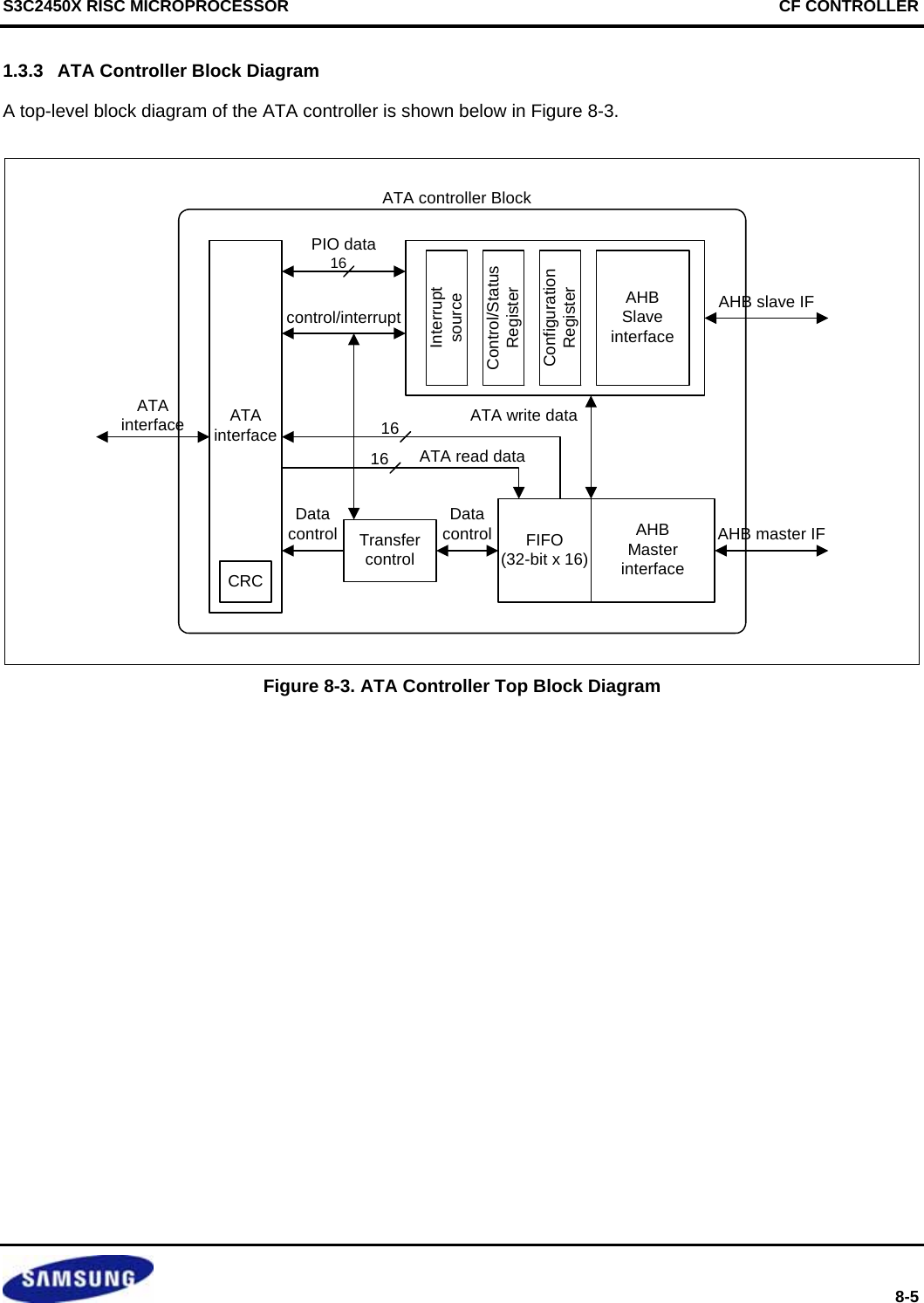
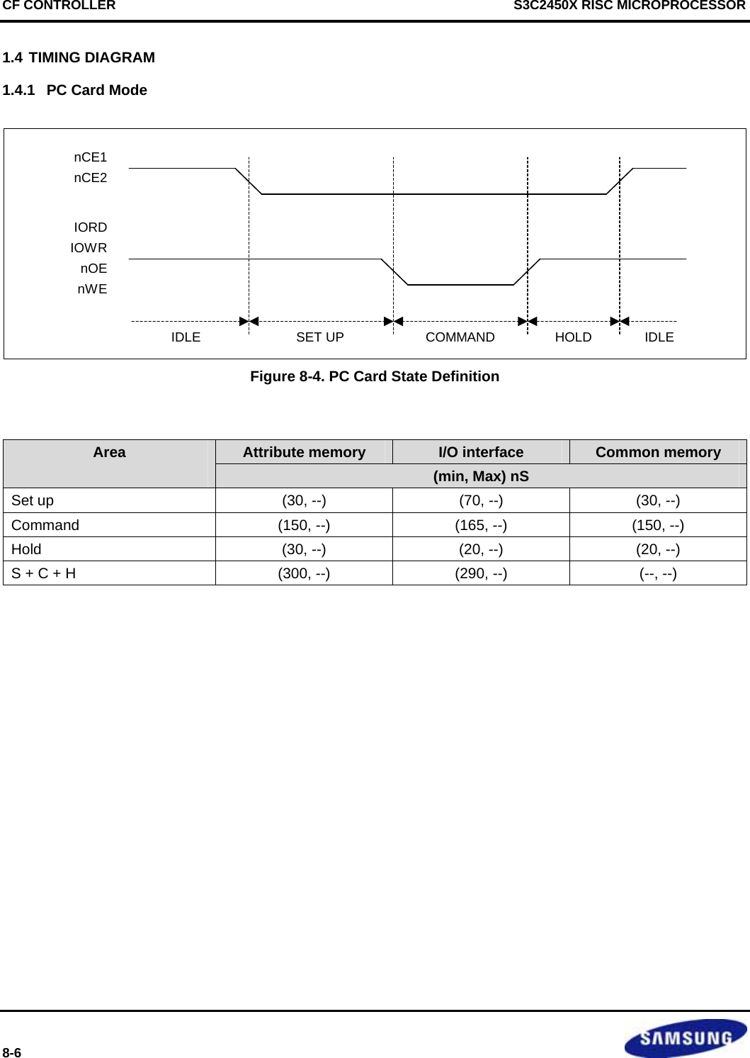
![S3C2450X RISC MICROPROCESSOR CF CONTROLLER 8-7 1.4.2 True-IDE Mode 1.4.3 PIO Mode PIO Mode Waveform t2t1teoct1CS0, CS1DA[2:0]DIOR-/DIOW-WRDD[15:0] orDD[7:0]RDDD[15:0] orDD[7:0] Figure 8-5. PIO Mode Waveform 1.4.4 Timing Parameter In PIO Mode Table 8-1. Timing Parameter Each PIO Mode PIO mode PIO 0 PIO 1 PIO 2 PIO 3 PIO 4 T1 (70, --) (50, --) (30, --) (30, --) (25, --) T2 (16bit) (165, --) (125, --) (100, --) (80, --) (70, --) T2 Register (8-bit) (290, --) (290, --) (290, --) (80, --) (70, --) TEOC (20, --) (15, --) (10, --) (10, --) (10, --) T1 + T2 + TEOC (600, --) (383, --) (240, --) (180, --) (120, --) ATA_PIO_TIME (Tpara) = PIO mode (min, max) / system clock − 1](https://usermanual.wiki/Diasonic-Technology-Co/RVM-704M.Users-Manual/User-Guide-1826140-Page-207.png)
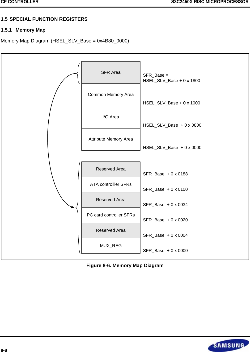
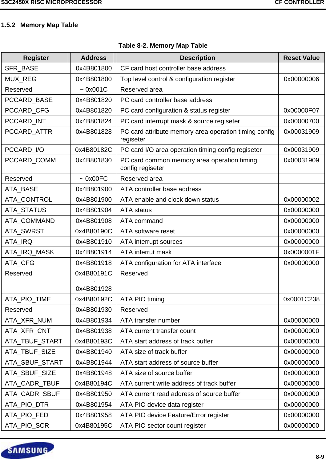
![S3C2450X RISC MICROPROCESSOR CF CONTROLLER 8-11 2 INDIVIDUAL REGISTER DESCRIPTIONS 2.1 MUX_REG REGISTER Register Address R/W Description Reset ValueMUX_REG 0x4B801800 R/W MUX_REG is used to set the internal mode, output port enable & card power enable. 0x0000_0006 MUX_REG Bit Description R/W Reset ValueReserved [31:3] Reserved bits R 0x0 OUTPUT_EN [2] Output port enable 0 = Output port enable 1 = Output port disable R/W 0x1 CARDPWR_EN [1] Card power supply enable 0 = Card power on 1 = Card power off R/W 0x1 IDE_MODE [0] Internal operation mode select 0 = PC card mode 1 = True-IDE mode R/W 0x0](https://usermanual.wiki/Diasonic-Technology-Co/RVM-704M.Users-Manual/User-Guide-1826140-Page-211.png)
![CF CONTROLLER S3C2450X RISC MICROPROCESSOR 8-12 2.2 PCCARD CONFIGURATION & STATUS REGISTER Register Address R/W Description Reset ValuePCCARD_CFG 0x4B801820 R/W PCCARD_CFG is used to set the configuration & read the status of card. 0x0000_0F07 PCCARD_CFG Bits Description R/W Reset ValueReserved [31:14] Reserved bits R 0x0 CARD_ RESET [13] CF card reset in PC card mode 0 = No reset 1 = Reset R/W 0x0 INT_SEL [12] Card interrupt request type select 0 = Edge triggering 1 = Level triggering R/W 0x0 nWAIT_EN [11] nWAIT(from CF card) enable 0 = Disable(always ready) 1 = Enable R/W 0x1 DEVICE_ATT [10] Device type is 16bits or 8bits (Attribute memory area) 0 = 8-bit device 1 = 16-bit device R/W 0x1 DEVICE_ COMM [9] Device type is 16bits or 8bits (Common memory area) 0 = 8-bit device 1 = 16-bit device R/W 0x1 DEVICE_IO [8] Device type is 16bits or 8bits (I/O area) 0 = 8-bit device 1 = 16-bit device R/W 0x1 Reserved [7:4] Reserved bits R 0x0 NOCARD_ERR [3] No card operation 0 = No error 1 = Error R 0x0 nWAIT [2] nWAIT from CF card 0 = Wait 1 = Ready R 0x1 nIREQ [1] Interrupt request from CF card 0 = Interrupt request 1 = No interrupt request R 0x1 nCD [0] Card detect 0 = Card detect 1 = Card not detect R 0x1](https://usermanual.wiki/Diasonic-Technology-Co/RVM-704M.Users-Manual/User-Guide-1826140-Page-212.png)
![S3C2450X RISC MICROPROCESSOR CF CONTROLLER 8-13 2.3 PCCARD INTERRUPT MASK & SOURCE REGISTER Register Address R/W Description Reset ValuePCCARD_INT 0x4B801824 R/W PCCARD_INT is interrupt source & interrupt mask register. 0x0000_0600 PCCARD_INT Bits Description R/W Reset ValueReserved [31:11] Reserved bits R 0x0 INTMSK_ERR_N [10] Interrupt mask bit of no card error 0 = Unmask 1 = Mask R/W 0x1 INTMSK_IREQ [9] Interrupt mask bit of CF card interrupt request 0 = Unmask 1 = Mask R/W 0x1 INTMSK_CD [8] Interrupt mask bit of CF card detect 0 = Unmask 1 = Mask R/W 0x0 Reserved [7:3] Reserved bits R 0x0 INTSRC_ERR_N [2] When host access no card in slot. CPU can clear this interrupt by writing “1”. R/W 0x0 INTSRC_IREQ [1] When CF card interrupt request CPU can clear this interrupt by writing “1”. R/W 0x0 INTSRC_CD [0] When CF card is detected in slot CPU can clear this interrupt by writing “1”. R/W 0x0](https://usermanual.wiki/Diasonic-Technology-Co/RVM-704M.Users-Manual/User-Guide-1826140-Page-213.png)
![CF CONTROLLER S3C2450X RISC MICROPROCESSOR 8-14 2.4 PCCARD_ATTR REGISTER Register Address R/W Description Reset ValuePCCARD_ATTR 0x4B801828 R/W PCCARD_ATTR is used to set the card access timing. 0x0003_1909 PCCARD_ATTR Bits Description R/W Reset ValueReserved [31:23] Reserved bits R 0x0 HOLD_ATTR [22:16] Hold state timing of attribute memory area Hold time = HCLK time * (HOLD_ATTR + 1) R/W 0x03 Reserved [15] Reserved bits R 0x0 CMND_ATTR [14:8] Command state timing of attribute memory area Command time = HCLK time * (CMND_ATTR + 1) R/W 0x19 Reserved [7] Reserved bits R 0x0 SETUP_ATTR [6:0] Setup state timing of attribute memory area Setup time = HCLK time * (SETUP_ATTR + 1) R/W 0x09 2.5 PCCARD_I/O REGISTER Register Address R/W Description Reset ValuePCCARD_I/O 0x4B80182C R/W PCCARD_I/O is used to set the card access timing. 0x0003_1909 PCCARD_I/O Bits Description R/W Reset ValueReserved [31:23] Reserved bits R 0x0 HOLD_IO [22:16] Hold state timing of I/O area Hold time = HCLK time * (HOLD_IO + 1) R/W 0x03 Reserved [15] Reserved bits R 0x0 CMND_IO [14:8] Command state timing of I/O area Command time = HCLK time * (CMND_IO + 1) R/W 0x19 Reserved [7] Reserved bits R 0x0 SETUP_IO [6:0] Setup state timing of I/O area Setup time = HCLK time * (SETUP_IO + 1) R/W 0x09](https://usermanual.wiki/Diasonic-Technology-Co/RVM-704M.Users-Manual/User-Guide-1826140-Page-214.png)
![S3C2450X RISC MICROPROCESSOR CF CONTROLLER 8-15 2.6 PCCARD_COMM REGISTER Register Address R/W Description Reset ValuePCCARD_COMM 0x4B801830 R/W PCCARD_COMM is used to set the card access timing. 0x0003_1909 PCCARD_COMM Bits Description R/W Reset ValueReserved [31:23] Reserved bits R 0x0 HOLD_COMM [22:16] Hold state timing of common memory area Hold time = HCLK time * (HOLD_COMM + 1) R/W 0x03 Reserved [15] Reserved bits R 0x0 CMND_COMM [14:8] Command state timing of common memory area Command time = HCLK time * (CMND_COMM + 1) R/W 0x19 Reserved [7] Reserved bits R 0x0 SETUP_COMM [6:0] Setup state timing of common memory area Setup time = HCLK time * (SETUP_COMM + 1) R/W 0x09](https://usermanual.wiki/Diasonic-Technology-Co/RVM-704M.Users-Manual/User-Guide-1826140-Page-215.png)
![CF CONTROLLER S3C2450X RISC MICROPROCESSOR 8-16 2.7 ATA_CONTROL REGISTER Register Address R/W Description Reset ValueATA_CONTROL 0x4B801900 R/W ATA Control register 0x0000_0002 ATA_CONTROL Bits Description R/W Reset ValueReserved [31:2] Reserved bits R 0x0 clk_down_ready [1] Status for clock down This bit is asserted in idle state when ATA_CONTROL bit [0] is zero. 0 = not ready for clock down 1 = ready for clock down R 0x1 ata_enable [0] ATA enable 0 = ATA is disabled and preparation for clock down maybe in progress 1 = ATA is enabled. R/W 0x0 2.8 ATA_STATUS REGISTER Register Address R/W Description Reset ValueATA_STATUS 0x4B801904 R ATA Status register 0x0000_0000 ATA_STATUS Bits Description R/W Reset ValueReserved [31:6] Reserved bits R 0x0 atadev_cblid [5] ATA cable identification R 0x0 atadev_irq [4] ATA interrupt signal line R 0x0 atadev_iordy [3] ATA iordy signal line R 0x0 atadev_dmareq [2] ATA dmareq signal line R 0x0 xfr_state [1:0] Transfer state 2’b00 = Idle state 2’b01 = Transfer state 2’b11 = Wait for completion state R 0x0](https://usermanual.wiki/Diasonic-Technology-Co/RVM-704M.Users-Manual/User-Guide-1826140-Page-216.png)
![S3C2450X RISC MICROPROCESSOR CF CONTROLLER 8-17 2.9 ATA_COMMAND REGISTER Register Address R/W Description Reset ValueATA_COMMAND 0x4B801908 R/W ATA Command register 0x0000_0000 ATA_COMMAND Bits Description R/W Reset ValueReserved [31:2] Reserved bits R 0x0 xfr_command [1:0] ATA transfer command Four command types (START, STOP, ABORT and CONTINUE) are supported for data transfer control. The “START” command is used to start data transfer. The “STOP” command can pause transfer temporarily. The “CONTINUE” command shall be used after “STOP” command or internal state of “pause” when track buffer is full. The “ABORT” command terminated current data transfer sequences and make ATA host controller move to idle state. 00 = command stop 01 = command start (Only available in idle state) 10 = command abort 11 = command continue (Only available in transfer pause) ** After CPU commands ABORT, make a software reset by ATA_SWRST to clear the leftover values of internal registers. R/W 0x0 The STOP command is a thing, which use when CPU wants to pause upon data transfer. When the CPU wants to judge the transmission data is valid or not while transfer transmits, for a moment. To send data continually, give a CONTINUE command to do data transmission continuously. The STOP command does control ATA Device side signal but does not control DMA side. Namely, if the FIFO has data after STOP command, DMA operation progresses until the FIFO has empty at read operation. In case of write operation, the DMA acts the same way until the FIFO has full. The ABORT command uses when the transmitting data has proved useless data or discontinues absurd state by error interrupt from device. At that time, all data in ATA Host controller (register, FIFO) cleared and the transmission state machine goes to IDLE. The Software Reset's meaning become clear all registers even though the ABORT command had been executed before do configuration register set for next transmission. But it is not mandatory.](https://usermanual.wiki/Diasonic-Technology-Co/RVM-704M.Users-Manual/User-Guide-1826140-Page-217.png)
![CF CONTROLLER S3C2450X RISC MICROPROCESSOR 8-18 2.10 ATA_SWRST REGISTER Register Address R/W Description Reset ValueATA_SWRST 0x4B80190C R/W ATA S/W RESET register 0x0000_0000 ATA_SWRST Bits Description R/W Reset ValueReserved [31:1] Reserved bits R 0x0 ata_swrstn [0] Software reset for the ATA host 0 = No reset 1 = Software reset for all ATA host module. After software reset, to continue transfer, user must configure all registers of host controller and device registers. R/W 0x0 2.11 ATA_IRQ REGISTER Register Address R/W Description Reset ValueATA_IRQ 0x4B801910 R/W ATA IRQ register 0x0000_0000 ATA_IRQ Bits Description R/W Reset ValueReserved [31:5] Reserved bits R 0x0 sbuf_empty_int [4] When source buffer is empty. CPU can clear this interrupt by writing “1”. R/W 0x0 tbuf_full_int [3] When track buffer is half full. CPU can clear this interrupt by writing “1”. R/W 0x0 atadev_irq_int [2] When ATA device generates interrupt. CPU can clear this interrupt by writing “1”. R/W 0x0 reserved [1] reserved R/W 0x0 xfr_done_int [0] When all data transfers are finished. CPU can clear this interrupt by writing “1”. R/W 0x0](https://usermanual.wiki/Diasonic-Technology-Co/RVM-704M.Users-Manual/User-Guide-1826140-Page-218.png)
![S3C2450X RISC MICROPROCESSOR CF CONTROLLER 8-19 2.12 ATA_IRQ_MASK REGISTER Register Address R/W Description Reset Value ATA_IRQ_MASK 0x4B801914 R/W ATA IRQ MASK register 0x0000_001F ATA_IRQ_MASK Bits Description R/W Reset ValueReserved [31:5] Reserved bits R 0x0 mask_sbut_ empty_int [4] Interrupt mask bit of source buffer empty 0 = Unmask 1 = Mask R/W 0x1 mask_tbuf_ full_int [3] Interrupt mask bit of target buffer full 0 = Unmask 1 = Mask R/W 0x1 mask_atadev_ irq_int [2] Interrupt mask bit of ATA device interrupt request 0 = Unmask 1 = Mask R/W 0x1 reserved [1] Reserved R/W 0x1 mask_xfr_ done_int [0] Interrupt mask bit of XFR done 0 = Unmask 1 = Mask R/W 0x1](https://usermanual.wiki/Diasonic-Technology-Co/RVM-704M.Users-Manual/User-Guide-1826140-Page-219.png)
![CF CONTROLLER S3C2450X RISC MICROPROCESSOR 8-20 2.13 ATA_CFG REGISTER Register Address R/W Description Reset ValueATA_CFG 0x4B801918 R/W ATA Configuration register 0x0000_0000 ATA_CFG Bits Description R/W Reset ValueReserved [31:9] Reserved bits R 0x0 sbuf_empty_ mode [8] Determines whether to continue automatically when source buffer is empty. This bit should not be changed during runtime operation. 0 = Continue automatically with new source buffer address. 1 = Stay in pause state and wait for CPU’s action. ** With the sbuf_empty mode is "0" and the transmission data size is bigger than the source buffer size, the source buffer empty interrupt(sbuf_empty_int) happens before setting of the second source buffer base address and size. Then ATA host controller brings data from the first source buffer repeatedly. To avoid this, after 1st source buffer is empty, the “sbuf_empty_mode” bit automatically goes to HIGH even though the default is “0”. So user must make a command “CONTINUE”. And then user don’t want that the CPU dose not interfere the change of the next source buffer address, set “0” at the bit 8 before/after the next base address and size. R/W 0x0 tbuf_full_mode [7] Determines whether to continue automatically when track buffer is full. This bit should not be changed during runtime operation. 0 = Continue automatically with new track buffer address. 1 = Stay in pause state and wait for CPU’s action. ** With the tbuf_full mode is "0" and the transmission data size is bigger than the target buffer size, the target buffer full interrupt(tbuf_full_int) happens before setting of the second target buffer base address and size. Then ATA host controller sends data to the first target buffer repeatedly. To avoid this, after 1st target buffer is full, the “tbuf_buf_mode” bit automatically goes to HIGH even though the default is “0”. So user must make a command “CONTINUE”. And then user don’t want that the CPU dose not interfere the change of the next target buffer address, set “0” at the bit 8 before/after the next base address and size. R/W 0x0 byte_swap [6] Determines whether data endian is little or big in 16bit data. 0 = Little endian ( data[15:8], data[7:0] ) 1 = Big endian ( data[7:0], data[15:8] ) R/W 0x0 atadev_irq_al [5] Device interrupt signal level 0 = Active high R/W 0x0](https://usermanual.wiki/Diasonic-Technology-Co/RVM-704M.Users-Manual/User-Guide-1826140-Page-220.png)
![S3C2450X RISC MICROPROCESSOR CF CONTROLLER 8-21 ATA_CFG Bits Description R/W Reset Value1 = Active low dma_dir [4] DMA transfer direction 0 = Host read data from device 1 = Host write data to device R/W 0x0 ata_class [3:2] ATA transfer class select 0 = Transfer class is PIO 1 = Transfer class is PIO DMA 2,3 = Reserved R/W 0x0 ata_iordy_en [1] Determines whether IORDY input can extend data transfer. 0 = IORDY disable( ignored ) 1 = IORDY enable ( can extend ) R/W 0x0 ata_rst [0] ATA device reset by this host. 0 = No reset 1 = Reset R/W 0x0](https://usermanual.wiki/Diasonic-Technology-Co/RVM-704M.Users-Manual/User-Guide-1826140-Page-221.png)
![CF CONTROLLER S3C2450X RISC MICROPROCESSOR 8-22 2.14 ATA_PIO_TIME REGISTER Register Address R/W Description Reset ValueATA_PIO_TIME 0x4B80192C R/W ATA PIO Timing Control register 0x0001_C238 ATA_PIO_TIME Bits Description R/W Reset ValueReserved [31:20] Reserved bits R 0x0 pio_teoc [19:12] PIO timing parameter, teoc, end of cycle time It shall not have zero value. teoc = HCLK time * (pio_teoc + 1) R/W 0x1C pio_t2 [11:4] PIO timing parameter, t2, DIOR/Wn pulse width It shall not have zero value. t2 = HCLK time * (pio_t2 + 1) R/W 0x23 pio_t1 [3:0] PIO timing parameter, t1, address valid to DIOR/Wn t1 = HCLK time * (pio_t1 + 1) R/W 0x8 2.15 ATA_XFR_NUM REGISTER Register Address R/W Description Reset ValueATA_XFR_NUM 0x4B801934 R/W ATA Data Transfer Number register 0x0000_0000 ATA_XFR_NUM Bits Description R/W Reset Valuexfr_num [31:1] Data transfer number. R/W 0x00000000Reserved [0] Reserved bits R 0x0 2.16 ATA_XFR_CNT REGISTER Register Address R/W Description Reset ValueATA_XFR_CNT 0x4B801938 R/W ATA Data Transfer Counter register 0x0000_0000 ATA_XFR_CNT Bits Description R/W Reset Valuexfr_cnt [31:1] Current remaining transfer counter. This value counts down from ATA_XFR_NUM. It goes to zero when pre-defined all data has been transferred. R/W 0x00000000Reserved [0] Reserved bits R 0x0](https://usermanual.wiki/Diasonic-Technology-Co/RVM-704M.Users-Manual/User-Guide-1826140-Page-222.png)
![S3C2450X RISC MICROPROCESSOR CF CONTROLLER 8-23 2.17 ATA_TBUF_START REGISTER Register Address R/W Description Reset ValueATA_TBUF_ START 0x4B80193C R/W Start address of track buffer 0x0000_0000 ATA_TBUF_ START Bits Description R/W Reset Valuetrack_buffer_ start [31:2] Start address of track buffer (4byte unit) R/W 0x00000000Reserved [1:0] Reserved bits R 0x0 2.18 ATA_TBUF_SIZE REGISTER Register Address R/W Description Reset ValueATA_TBUF_ SIZE 0x4B801940 R/W Size of track buffer 0x0000_0000 ATA_TBUF_ SIZE Bits Description R/W Reset Valuetrack_buffer_ size [31:5] Size of track buffer (32byte unit) This should be set to “size_of_data_in_bytes − 1”. For example, to transfer 1-sector (512-byte, 32’h200), user should set 32’h1FF ( = 32’h200 – 1). R/W 0x0000000 Reserved [4:0] Reserved bits R 0x00](https://usermanual.wiki/Diasonic-Technology-Co/RVM-704M.Users-Manual/User-Guide-1826140-Page-223.png)
![CF CONTROLLER S3C2450X RISC MICROPROCESSOR 8-24 2.19 ATA_SBUF_START REGISTER Register Address R/W Description Reset ValueATA_SBUF_ START 0x4B801944 R/W Start address of source buffer 0x0000_0000 ATA_SBUF_ START Bits Description R/W Reset Valuesrc_buffer_start [31:2] Start address of source buffer (4byte unit) R/W 0x00000000Reserved [1:0] Reserved bits R 0x0 2.20 ATA_SBUF_SIZE REGISTER Register Address R/W Description Reset ValueATA_SBUF_ SIZE 0x4B801948 R/W Size of source buffer 0x0000_0000 ATA_SBUF_ SIZE Bits Description R/W Reset Valuesrc_buffer_ size [31:5] Size of source buffer (32byte unit) This should be set to “size_of_data_in_bytes – 1”. For example, to transfer 1-sector (512-byte, 32’h200), user should set 32’h1FF ( = 32’h200 – 1). R/W 0x0000000 Reserved [4:0] Reserved bits R 0x00](https://usermanual.wiki/Diasonic-Technology-Co/RVM-704M.Users-Manual/User-Guide-1826140-Page-224.png)
![S3C2450X RISC MICROPROCESSOR CF CONTROLLER 8-25 2.21 ATA_CADDR_TBUF REGISTER Register Address R/W Description Reset ValueATA_CADDR_ TBUF 0x4B80194C R/W Current address of track buffer 0x0000_0000 ATA_CADDR_ TBUF Bits Description R/W Reset Valuetrack_buf_ cur_adr [31:2] Current address of track buffer R/W 0x00000000Reserved [1:0] Reserved bits R 0x0 2.22 ATA_CADDR_SBUF REGISTER Register Address R/W Description Reset ValueATA_CADDR_ SBUF 0x4B801950 R/W Current address of source buffer 0x0000_0000 ATA_CADDR_ SBUF Bits Description R/W Reset Valuesrc_buf_cur_ adr [31:2] Current address of source buffer R/W 0x00000000Reserved [1:0] Reserved bits R 0x0 2.23 ATA_PIO_DTR REGISTER Register Address R/W Description Reset ValueATA_PIO_DTR 0x4B801954 W 16bit PIO data register 0x0000_0000 ATA_PIO_DTR Bits Description R/W Reset ValueReserved [31:16] Reserved bits R 0x0 pio_dev_dtr* [15:0] 16-bit PIO data register W 0x0000 NOTE: pio_dev_dtr can be read by accessing register ATA_PIO_RDATA](https://usermanual.wiki/Diasonic-Technology-Co/RVM-704M.Users-Manual/User-Guide-1826140-Page-225.png)
![CF CONTROLLER S3C2450X RISC MICROPROCESSOR 8-26 2.24 ATA_PIO_FED REGISTER Register Address R/W Description Reset ValueATA_PIO_FED 0x4B801958 W 8bit PIO device feature/error register 0x0000_0000 ATA_PIO_FED Bits Description R/W Reset ValueReserved [31:8] Reserved bits R 0x0 pio_dev_fed [7:0] 8-bit PIO device feature/error (command block) register W 0x00 NOTE: pio_dev_fed can be read by accessing register ATA_PIO_RDATA 2.25 ATA_PIO_SCR REGISTER Register Address R/W Description Reset ValueATA_PIO_SCR 0x4B80195C W 8-bit PIO device sector count register 0x0000_0000 ATA_PIO_SCR Bits Description R/W Reset ValueReserved [31:8] Reserved bits R 0x0 pio_dev_scr [7:0] 8-bit PIO device sector count (command block) register W 0x00 NOTE: pio_dev_scr can be read by accessing register ATA_PIO_RDATA 2.26 ATA_PIO_LLR REGISTER Register Address R/W Description Reset ValueATA_PIO_LLR 0x4B801960 W 8-bit PIO device LBA low register 0x0000_0000 ATA_PIO_LLR Bits Description R/W Reset ValueReserved [31:8] Reserved bits R 0x0 pio_dev_llr [7:0] 8-bit PIO device LBA low (command block) register W 0x00 NOTE: pio_dev_llr can be read by accessing register ATA_PIO_RDATA](https://usermanual.wiki/Diasonic-Technology-Co/RVM-704M.Users-Manual/User-Guide-1826140-Page-226.png)
![S3C2450X RISC MICROPROCESSOR CF CONTROLLER 8-27 2.27 ATA_PIO_LMR REGISTER Register Address R/W Description Reset ValueATA_PIO_LMR 0x4B801964 W 8-bit PIO device LBA middle register 0x0000_0000 ATA_PIO_LMR Bits Description R/W Reset ValueReserved [31:8] Reserved bits R 0x0 pio_dev_lmr [7:0] 8-bit PIO device LBA middle (command block) register W 0x00 NOTE: pio_dev_lmr can be read by accessing register ATA_PIO_RDATA 2.28 ATA_PIO_LMR REGISTER Register Address R/W Description Reset ValueATA_PIO_LHR 0x4B801968 W 8-bit PIO device LBA high register 0x0000_0000 ATA_PIO_LHR Bits Description R/W Reset ValueReserved [31:8] Reserved bits R 0x0 pio_dev_lhr [7:0] 8-bit PIO LBA high (command block) register W 0x00 NOTE: pio_dev_lhr can be read by accessing register ATA_PIO_RDATA 2.29 ATA_PIO_DVR REGISTER Register Address R/W Description Reset ValueATA_PIO_DVR 0x4B80196C W 8-bit PIO device register 0x0000_0000 ATA_PIO_DVR Bits Description R/W Reset ValueReserved [31:8] Reserved bits R 0x0 pio_dev_dvr [7:0] 8-bit PIO device (command block) register W 0x00 NOTE: pio_dev_dvr can be read by accessing register ATA_PIO_RDATA](https://usermanual.wiki/Diasonic-Technology-Co/RVM-704M.Users-Manual/User-Guide-1826140-Page-227.png)
![CF CONTROLLER S3C2450X RISC MICROPROCESSOR 8-28 2.30 ATA_PIO_CSD REGISTER Register Address R/W Description Reset ValueATA_PIO_CSD 0x4B801970 W 8-bit PIO device command/status register 0x0000_0000 ATA_PIO_CSD Bits Description R/W Reset ValueReserved [31:8] Reserved bits R 0x0 pio_dev_csd [7:0] 8-bit PIO device command/status (command block) register W 0x00 NOTE: pio_dev_csd can be read by accessing register ATA_PIO_RDATA 2.31 ATA_PIO_DAD REGISTER Register Address R/W Description Reset ValueATA_PIO_DAD 0x4B801974 W 8-bit PIO device control/alternate status register 0x0000_0000 ATA_PIO_DAD Bits Description R/W Reset ValueReserved [31:8] Reserved bits R 0x0 pio_dev_dad [7:0] 8-bit PIO device control/alternate status (control block) register W 0x00 NOTE: pio_dev_dad can be read by accessing register ATA_PIO_RDATA 2.32 ATA_PIO_RDATA REGISTER Register Address R/W Description Reset ValueATA_PIO_ RDATA 0x4B80197C R PIO read data register 0x0000_0000 ATA_PIO_ RDATA Bits Description R/W Reset ValueReserved [31:16] Reserved bits R 0x0 pio_rdata [15:0] PIO read data register while HOST read from ATA device register R 0x0000](https://usermanual.wiki/Diasonic-Technology-Co/RVM-704M.Users-Manual/User-Guide-1826140-Page-228.png)
![S3C2450X RISC MICROPROCESSOR CF CONTROLLER 8-29 2.33 BUS_FIFO_STATUS REGISTER Register Address R/W Description Reset ValueBUS_FIFO_ STATUS 0x4B801990 R BUS FIFO status register 0x0000_0000 BUS_FIFO_ STATUS Bits Description R/W Reset ValueReserved [31:19] Reserved bits R 0x0 bus_state[2:0] [18:16] 3’b000 : IDLE Another value is in operation. R 0x00 Reserved [15:14] Reserved bits R 0x0 bus_fifo_rdpnt [13:8] bus fifo read pointer R 0x00 Reserved [7:6] Reserved bits R 0x0 bus_fifo_wrpnt [5:0] bus fifo write pointer R 0x00 2.34 ATA_FIFO_STATUS REGISTER Register Address R/W Description Reset ValueATA_FIFO_ STATUS 0x4B801994 R ATA FIFO status register 0x0000_0000 ATA_FIFO_ STATUS Bits Description R/W Reset ValueReserved [31] Reserved bit R 0x0 ata_state [30:28] PIO read data register while HOST read from ATA device register R 0x0000 pio_state [27:26] 2’b00 = IDLE 2’’b01 = T1 2’b10 = T2 2’b11 = TEOC R 0x0 pdma_state [25:24] 2’b00 = IDLE 2’b01 = T1 2’b10 = T2 2’b11 = TEOC R 0x0 Reserved [23:0] Reserved bits R 0x0](https://usermanual.wiki/Diasonic-Technology-Co/RVM-704M.Users-Manual/User-Guide-1826140-Page-229.png)

![DMA CONTROLLER S3C2450X RISC MICROPROCESSOR 9-2 2 DMA REQUEST SOURCES Each channel of DMA controller can select one source among 27 DMA sources if H/W DMA request mode is selected by REQSEL register. (Note that if S/W request mode is selected, this DMA request sources have no meaning at all.) The 27 DMA sources for each channel are as follows. Table 9-1. DMA request sources for each channel Bit Source Bit Source Bit Source Bit Source 0 SPI_0_TX 8 Reserved 16 Reserved 24 UART_2[1] 1 SPI_0_RX 9 PWM Timer 17 nXDREQ0 25 UART_3[0] 2 SPI_1_TX 10 Reserved 18 nXDREQ1 26 UART_3[1] 3 SPI_1_RX 11 Reserved 19 UART_0[0] 27 PCMOUT 4 I2S TX 12 PCM0 TX 20 UART_0[1] 28 PCMIN 5 I2S RX 13 PCM0 RX 21 UART_1[0] 29 MICIN 6 I2S1 TX 14 PCM1 TX 22 UART_1[1] 30 Reserved 7 I2S1 RX 15 PCM1 RX 23 UART_2[0] 31 Reserved Here, nXDREQ0 and nXDREQ1 represent two external sources (External Devices).](https://usermanual.wiki/Diasonic-Technology-Co/RVM-704M.Users-Manual/User-Guide-1826140-Page-232.png)
![S3C2450X RISC MICROPROCESSOR DMA CONTROLLER 9-3 3 DMA OPERATION The details of DMA operation can be explained using three-state FSM (finite state machine) as follows: State-1. As an initial state, it waits for the DMA request. If it comes, go to state-2. At this state, DMA ACK and INT REQ are 0. State-2. In this state, DMA ACK becomes 1 and the counter (CURR_TC) is loaded from DCON[19:0] register. Note that DMA ACK becomes 1 and remains 1 until it is cleared later. State-3. In this state, sub-FSM handling the atomic operation of DMA is initiated. The sub-FSM reads the data from the source address and then writes it to destination address. In this operation, data size and transfer size (single or burst) are considered. This operation is repeated until the counter (CURR_TC) becomes 0 in the whole service mode, while performed only once in a single service mode. The main FSM (this FSM) counts down the CURR_TC when the sub-FSM finishes each of atomic operation. In addition, this main FSM asserts the INT REQ signal when CURR_TC becomes 0 and the interrupt setting of DCON [29] register is set to 1. In addition, it clears DMA ACK if one of the following conditions is met. 1) CURR_TC becomes 0 in the whole service mode 2) atomic operation finishes in the single service mode. Note that in the single service mode, these three states of main FSM are performed and then stops, and wait for another DMA REQ. And if DMA REQ comes in all three states are repeated. Therefore, DMA ACK is asserted and then de-asserted for each atomic transfer. In contrast, in the whole service mode, main FSM waits at state-3 until CURR_TC becomes 0. Therefore, DMA ACK is asserted during all the transfers and then de-asserted when TC reaches 0. However, INT REQ is asserted only if CURR_TC becomes 0 regardless of the service mode (single service mode or whole service mode).](https://usermanual.wiki/Diasonic-Technology-Co/RVM-704M.Users-Manual/User-Guide-1826140-Page-233.png)
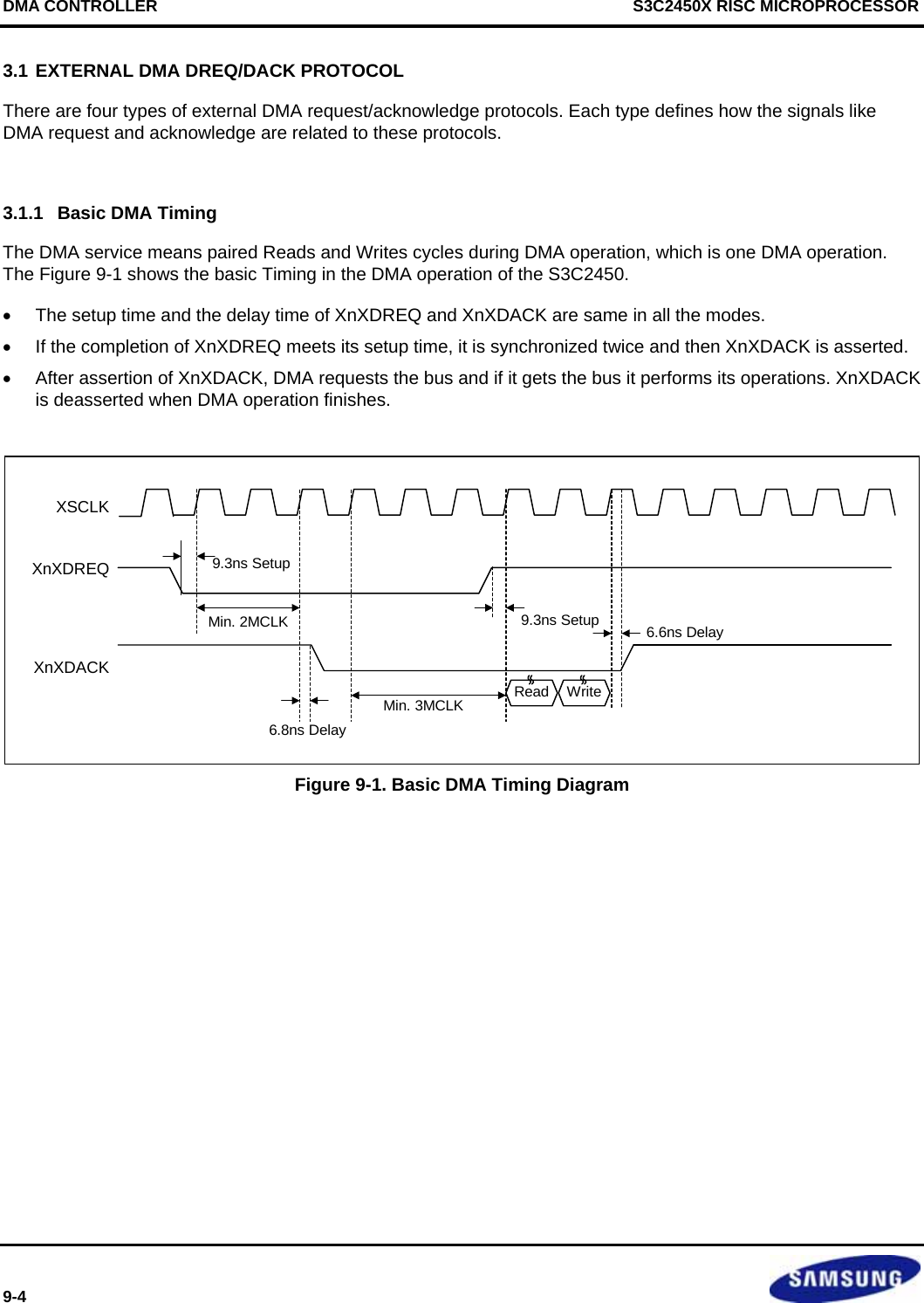
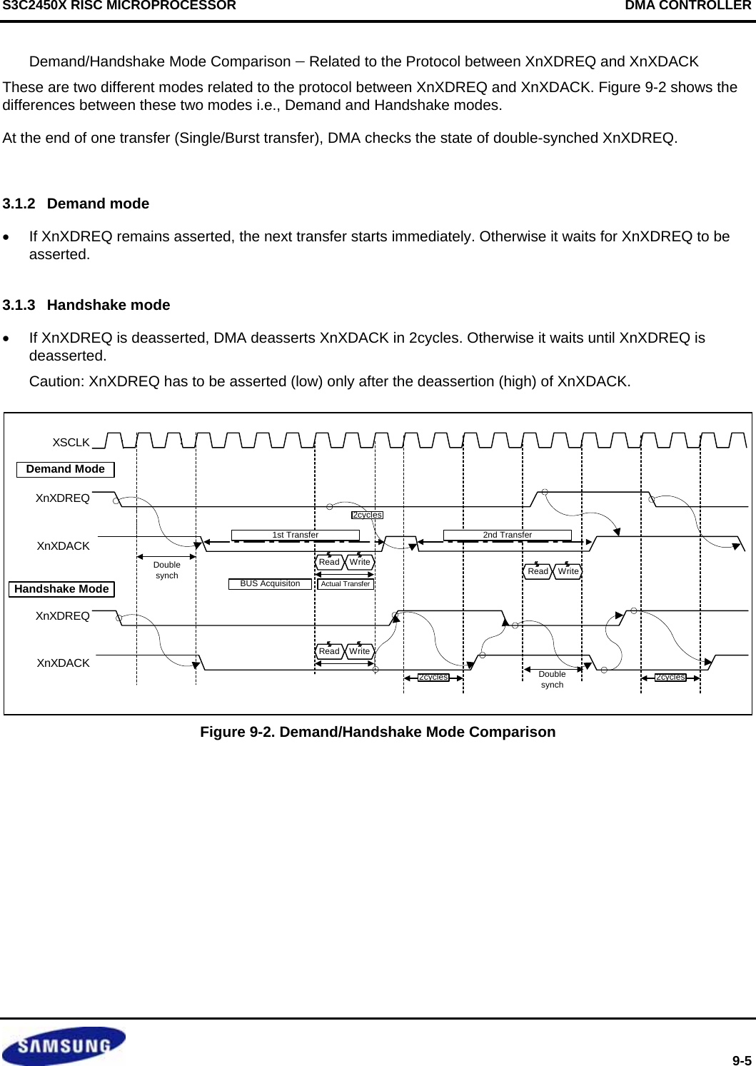
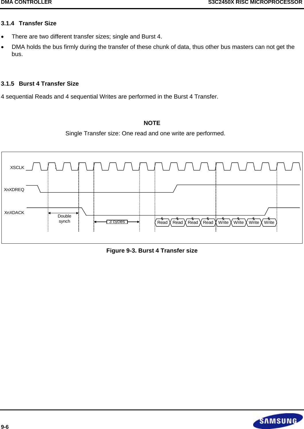
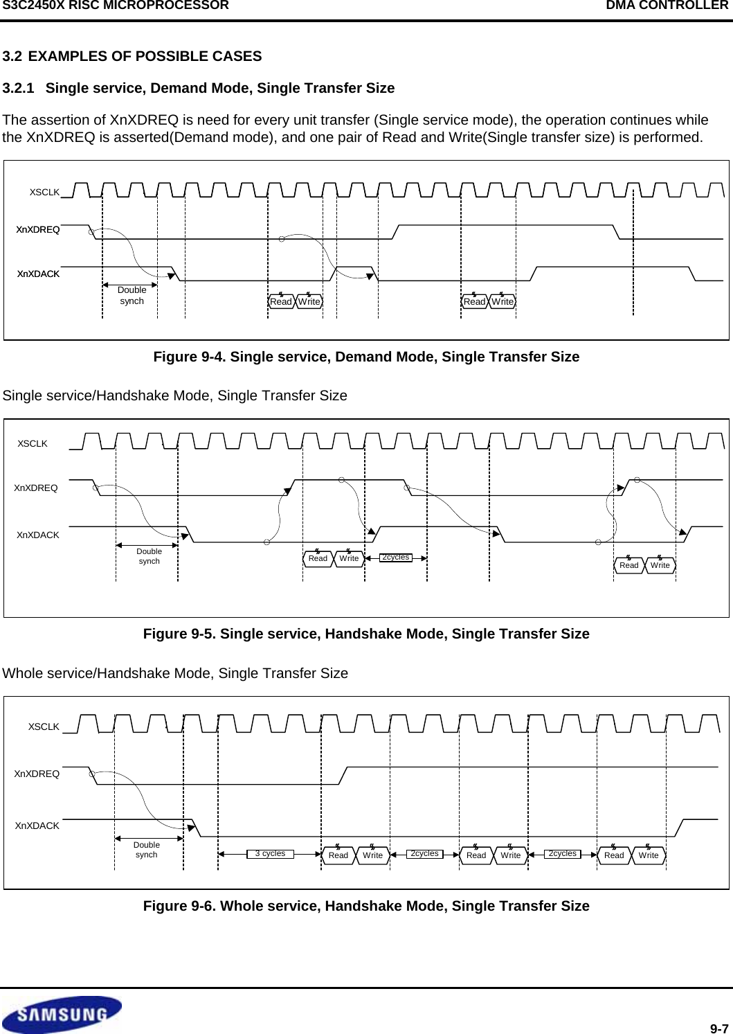
![DMA CONTROLLER S3C2450X RISC MICROPROCESSOR 9-8 4 DMA SPECIAL REGISTERS There are 10 control registers for each DMA channel. (Since there are six channels, the total number of control registers is 60.) Seven of them are to control the DMA transfer, and other three are to see the status of DMA controller. The details of those registers are as follows. 4.1 DMA INITIAL SOURCE REGISTER (DISRC) Register Address R/W Description Reset ValueDISRC0 0x4B000000 R/W DMA0 Initial Source Register 0x00000000DISRC1 0x4B000100 R/W DMA1 Initial Source Register 0x00000000DISRC2 0x4B000200 R/W DMA2 Initial Source Register 0x00000000DISRC3 0x4B000300 R/W DMA3 Initial Source Register 0x00000000DISRC4 0x4B000400 R/W DMA4 Initial Source Register 0x00000000DISRC5 0x4B000500 R/W DMA5 Initial Source Register 0x00000000DISRC6 0x4B000600 R/W DMA6 Initial Source Register 0x00000000DISRC7 0x4B000700 R/W DMA7 Initial Source Register 0x00000000 DISRCn Bit Description Initial State S_ADDR [30:0] These bits are the base address (start address) of source data to transfer. This value will be loaded into CURR_SRC only if the CURR_SRC is 0 and the DMA ACK is 1. 0x00000000](https://usermanual.wiki/Diasonic-Technology-Co/RVM-704M.Users-Manual/User-Guide-1826140-Page-238.png)
![S3C2450X RISC MICROPROCESSOR DMA CONTROLLER 9-9 4.2 DMA INITIAL SOURCE CONTROL REGISTER (DISRCC) Register Address R/W Description Reset ValueDISRCC0 0x4B000004 R/W DMA0 Initial Source Control Register 0x00000000DISRCC1 0x4B000104 R/W DMA1 Initial Source Control Register 0x00000000DISRCC2 0x4B000204 R/W DMA2 Initial Source Control Register 0x00000000DISRCC3 0x4B000304 R/W DMA3 Initial Source Control Register 0x00000000DISRCC4 0x4B000404 R/W DMA4 Initial Source Control Register 0x00000000DISRCC5 0x4B000504 R/W DMA5 Initial Source Control Register 0x00000000DISRCC6 0x4B000604 R/W DMA6 Initial Source Control Register 0x00000000DISRCC7 0x4B000704 R/W DMA7 Initial Source Control Register 0x00000000 DISRCn Bit Description Initial State LOC [1] Bit 1 is used to select the location of source. 0 = The source is in the system bus (AHB), 1 = The source is in the peripheral bus (APB) 0 INC [0] Bit 0 is used to select the address increment. 0 = Increment 1 = Fixed If it is 0, the address is increased by its data size after each transfer in burst and single transfer mode. If it is 1, the address is not changed after the transfer (In the burst mode, address is increased during the burst transfer, but the address is recovered to its first value after the transfer). 0](https://usermanual.wiki/Diasonic-Technology-Co/RVM-704M.Users-Manual/User-Guide-1826140-Page-239.png)
![DMA CONTROLLER S3C2450X RISC MICROPROCESSOR 9-10 4.3 DMA INITIAL DESTINATION REGISTER (DIDST) Register Address R/W Description Reset ValueDIDST0 0x4B000008 R/W DMA0 Initial Destination Register 0x00000000DIDST1 0x4B000108 R/W DMA1 Initial Destination Register 0x00000000DIDST2 0x4B000208 R/W DMA2 Initial Destination Register 0x00000000DIDST3 0x4B000308 R/W DMA3 Initial Destination Register 0x00000000DIDST4 0x4B000408 R/W DMA4 Initial Destination Register 0x00000000DIDST5 0x4B000508 R/W DMA5 Initial Destination Register 0x00000000DIDST6 0x4B000608 R/W DMA6 Initial Destination Register 0x00000000DIDST7 0x4B000708 R/W DMA7 Initial Destination Register 0x00000000 DIDSTn Bit Description Initial State D_ADDR [30:0] These bits are the base address (start address) of destination for the transfer. This value will be loaded into CURR_SRC only if the CURR_SRC is 0 and the DMA ACK is 1. 0x00000000](https://usermanual.wiki/Diasonic-Technology-Co/RVM-704M.Users-Manual/User-Guide-1826140-Page-240.png)
![S3C2450X RISC MICROPROCESSOR DMA CONTROLLER 9-11 4.4 DMA INITIAL DESTINATION CONTROL REGISTER (DIDSTC) Register Address R/W Description Reset ValueDIDSTC0 0x4B00000C R/W DMA0 Initial Destination Control Register 0x00000000DIDSTC1 0x4B00010C R/W DMA1 Initial Destination Control Register 0x00000000DIDSTC2 0x4B00020C R/W DMA2 Initial Destination Control Register 0x00000000DIDSTC3 0x4B00030C R/W DMA3 Initial Destination Control Register 0x00000000DIDSTC4 0x4B00040C R/W DMA4 Initial Destination Control Register 0x00000000DIDSTC5 0x4B00050C R/W DMA5 Initial Destination Control Register 0x00000000DIDSTC6 0x4B00060C R/W DMA6 Initial Destination Control Register 0x00000000DIDSTC7 0x4B00070C R/W DMA7 Initial Destination Control Register 0x00000000 DIDSTn Bit Description Initial State CHK_INT [2] Select interrupt occurrence time when auto reload is setting 0 = Interrupt will occur when TC reaches 0. 1 = Interrupt will occur after auto-reload is performed 0 LOC [1] Bit 1 is used to select the location of destination. 0 = The destination is in the system bus (AHB). 1 = The destination is in the peripheral bus (APB). 0 INC [0] Bit 0 is used to select the address increment. 0 = Increment 1 = Fixed If it is 0, the address is increased by its data size after each transfer in burst and single transfer mode. If it is 1, the address is not changed after the transfer (In the burst mode, address is increased during the burst transfer, but the address is recovered to its first value after the transfer). 0](https://usermanual.wiki/Diasonic-Technology-Co/RVM-704M.Users-Manual/User-Guide-1826140-Page-241.png)
![DMA CONTROLLER S3C2450X RISC MICROPROCESSOR 9-12 4.5 DMA CONTROL REGISTER (DCON) Register Address R/W Description Reset ValueDCON0 0x4B000010 R/W DMA0 Control Register 0x00000000DCON1 0x4B000110 R/W DMA1 Control Register 0x00000000DCON2 0x4B000210 R/W DMA2 Control Register 0x00000000DCON3 0x4B000310 R/W DMA3 Control Register 0x00000000DCON4 0x4B000410 R/W DMA4 Control Register 0x00000000DCON5 0x4B000510 R/W DMA5 Control Register 0x00000000DCON6 0x4B000610 R/W DMA6 Control Register 0x00000000DCON7 0x4B000710 R/W DMA7 Control Register 0x00000000 DCONn Bit Description Initial State DMD_HS [31] Select one between demand mode and handshake mode. 0 = demand mode is selected 1 = handshake mode is selected. In both modes, DMA controller starts its transfer and asserts DACK for a given asserted DREQ. The difference between two modes is whether it waits for the de-asserted DACK or not. In handshake mode, DMA controller waits for the de-asserted DREQ before starting a new transfer. If it sees the de-asserted DREQ, it de-asserts DACK and waits for another asserted DREQ. In contrast, in the demand mode, DMA controller does not wait until the DREQ is de-asserted. It just de-asserts DACK and then starts another transfer if DREQ is asserted. We recommend using handshake mode for external DMA request sources to prevent unintended starts of new transfers. 0 SYNC [30] Select DREQ/DACK synchronization. 0 = DREQ and DACK are synchronized to PCLK (APB clock). 1 = DREQ and DACK are synchronized to HCLK (AHB clock). Therefore, devices attached to AHB system bus, this bit has to be set to 1, while those attached to APB system, it should be set to 0. For the devices attached to external system, user should select this bit depending on whether the external system is synchronized with AHB system or APB system. 0 INT [29] Enable/Disable the interrupt setting for CURR_TC(terminal count) 0 = CURR_TC interrupt is disabled. User has to look the transfer count in the status register. (i.e., polling) 1 = Interrupt request is generated when all the transfer is done (i.e., CURR_TC becomes 0). 0 TSZ [28] Select the transfer size of an atomic transfer (i.e., transfer performed at each time DMA owns the bus before releasing the bus). 0 = A unit transfer is performed. 1 = A burst transfer of length four is performed. 0](https://usermanual.wiki/Diasonic-Technology-Co/RVM-704M.Users-Manual/User-Guide-1826140-Page-242.png)
![S3C2450X RISC MICROPROCESSOR DMA CONTROLLER 9-13 DCONn Bit Description Initial State SERVMODE [27] Select the service mode between single service mode and whole service mode. 0 = Single service mode is selected in which after each atomic transfer (single or burst of length four) DMA stops and waits for another DMA request. 1 = Whole service mode is selected in which one request gets atomic transfers to be repeated until the transfer count reaches to 0. In this mode, additional request is not required. Here, note that even in the whole service mode, DMA releases the bus after each atomic transfer and then tries to re-get the bus to prevent starving of other bus masters. 0 Reserved [26:25] Reserved for future use 00 PADDRFIX [24] APB Address fix control 0 = Increment 1 = Fix If you want to fix the APB address during burst operation, set this bit to 1. 0 Reserved [23] Reserved for future use 0 RELOAD [22] Set the reload on/off option. 0 = Auto reload is performed when a current value of transfer count becomes 0 (i.e., all the required transfers are performed). 1 = DMA channel (DMA REQ) is turned off when a current value of transfer count becomes 0. The channel on/off bit(DMASKTRIGn[1]) is set to 0(DREQ off) to prevent unintended further start of new DMA operation 0 DSZ [21:20] Data size to be transferred. 00 = Byte 01 = Half word 10 = Word 11 = Reserved 00 TC [19:0] Initial transfer count (or transfer beat). Note that the actual number of bytes that are transferred is computed by the following equation: DSZ x TSZ x TC, where DSZ, TSZ, and TC represent data size (DCONn[21:20]), transfer size (DCONn[28]), and initial transfer count, respectively. This value will be loaded into CURR_TC only if the CURR_TC is 0 and the DMA ACK is 1. 00000](https://usermanual.wiki/Diasonic-Technology-Co/RVM-704M.Users-Manual/User-Guide-1826140-Page-243.png)
![DMA CONTROLLER S3C2450X RISC MICROPROCESSOR 9-14 4.6 DMA STATUS REGISTER (DSTAT) Register Address R/W Description Reset ValueDSTAT0 0x4B000014 R DMA0 Count Register 000000h DSTAT1 0x4B000114 R DMA1 Count Register 000000h DSTAT2 0x4B000214 R DMA2 Count Register 000000h DSTAT3 0x4B000314 R DMA3 Count Register 000000h DSTAT4 0x4B000414 R DMA4 Count Register 000000h DSTAT5 0x4B000514 R DMA5 Count Register 000000h DSTAT6 0x4B000614 R DMA6 Count Register 000000h DSTAT7 0x4B000714 R DMA7 Count Register 000000h DSTATn Bit Description Initial StateSTAT [21:20] Status of this DMA controller. 00 = It indicates that DMA controller is ready for another DMA request. 01 = It indicates that DMA controller is busy for transfers. 00b CURR_TC [19:0] Current value of transfer count. Note that transfer count is initially set to the value of DCONn[19:0] register and decreased by one at the end of every atomic transfer. 00000h](https://usermanual.wiki/Diasonic-Technology-Co/RVM-704M.Users-Manual/User-Guide-1826140-Page-244.png)
![S3C2450X RISC MICROPROCESSOR DMA CONTROLLER 9-15 4.7 DMA CURRENT SOURCE REGISTER (DCSRC) Register Address R/W Description Reset ValueDCSRC0 0x4B000018 R DMA0 Current Source Register 0x00000000DCSRC1 0x4B000118 R DMA1 Current Source Register 0x00000000DCSRC2 0x4B000218 R DMA2 Current Source Register 0x00000000DCSRC3 0x4B000318 R DMA3 Current Source Register 0x00000000DCSRC4 0x4B000418 R DMA4 Current Source Register 0x00000000DCSRC5 0x4B000518 R DMA5 Current Source Register 0x00000000DCSRC6 0x4B000618 R DMA6 Current Source Register 0x00000000DCSRC7 0x4B000718 R DMA7 Current Source Register 0x00000000 DCSRCn Bit Description Initial State CURR_SRC [30:0] Current source address for DMAn. 0x00000000 4.8 CURRENT DESTINATION REGISTER (DCDST) Register Address R/W Description Reset ValueDCDST0 0x4B00001C R DMA0 Current Destination Register 0x00000000DCDST1 0x4B00011C R DMA1 Current Destination Register 0x00000000DCDST2 0x4B00021C R DMA2 Current Destination Register 0x00000000DCDST3 0x4B00031C R DMA3 Current Destination Register 0x00000000DCDST4 0x4B00041C R DMA4 Current Destination Register 0x00000000DCDST5 0x4B00051C R DMA5 Current Destination Register 0x00000000DCDST6 0x4B00061C R DMA6 Current Destination Register 0x00000000DCDST7 0x4B00071C R DMA7 Current Destination Register 0x00000000 DCDSTn Bit Description Initial State CURR_DST [30:0] Current destination address for DMAn. 0x00000000](https://usermanual.wiki/Diasonic-Technology-Co/RVM-704M.Users-Manual/User-Guide-1826140-Page-245.png)
![DMA CONTROLLER S3C2450X RISC MICROPROCESSOR 9-16 4.9 DMA MASK TRIGGER REGISTER (DMASKTRIG) Register Address R/W Description Reset ValueDMASKTRIG0 0x4B000020 R/W DMA0 Mask Trigger Register 000 DMASKTRIG1 0x4B000120 R/W DMA1 Mask Trigger Register 000 DMASKTRIG2 0x4B000220 R/W DMA2 Mask Trigger Register 000 DMASKTRIG3 0x4B000320 R/W DMA3 Mask Trigger Register 000 DMASKTRIG4 0x4B000420 R/W DMA4 Mask Trigger Register 000 DMASKTRIG5 0x4B000520 R/W DMA5 Mask Trigger Register 000 DMASKTRIG6 0x4B000620 R/W DMA6 Mask Trigger Register 000 DMASKTRIG7 0x4B000720 R/W DMA7 Mask Trigger Register 000 DMASKTRIGn Bit Description Initial State STOP [2] Stop the DMA operation. 1 = DMA stops as soon as the current atomic transfer ends. If there is no current running atomic transfer, DMA stops immediately. The CURR_TC, CURR_SRC, CURR_DST will be 0. Note: Due to possible current atomic transfer, “stop” may take several cycles. The finish of “stopping” operation (i.e., actual stop time) can be detected by waiting until the channel on/off bit (DMASKTRIGn[1]) is set to off. This stop is “actual stop”. 0 ON_OFF [1] DMA channel on/off bit. 0 = DMA channel is turned off. (DMA request to this channel is ignored.) 1 = DMA channel is turned on and the DMA request is handled. This bit is automatically set to off if we set the DCONn[22] bit to “no auto reload” and/or STOP bit of DMASKTRIGn to “stop”. Note that when DCON [22] bit is "no auto reload", this bit becomes 0 when CURR_TC reaches 0. If the STOP bit is 1, this bit becomes 0 as soon as the current atomic transfer finishes. Note: This bit should not be changed manually during DMA operations (i.e., this has to be changed only by using DCON [22] or STOP bit.) 0 SW_TRIG [0] Trigger the DMA channel in S/W request mode. 1 = it requests a DMA operation to this controller. However, note that for this trigger to have effects S/W request mode has to be selected (DCONn[23]) and channel ON_OFF bit has to be set to 1 (channel on). When DMA operation starts, this bit is cleared automatically. 0 NOTE: You can freely change the values of DISRC register, DIDST registers, and TC field of DCON register. Those changes take effect only after the finish of current transfer (i.e., when CURR_TC becomes 0). On the other hand, any change made to other registers and/or fields takes immediate effect. Therefore, be careful in changing those registers and fields.](https://usermanual.wiki/Diasonic-Technology-Co/RVM-704M.Users-Manual/User-Guide-1826140-Page-246.png)
![S3C2450X RISC MICROPROCESSOR DMA CONTROLLER 9-17 4.10 DMA REQUESET SELECTION REGISTER (DMAREQSEL) Register Address R/W Description Reset ValueDMAREQSEL0 0x4B000024 R/W DMA0 Request Selection Register 000 DMAREQSEL1 0x4B000124 R/W DMA1 Request Selection Register 000 DMAREQSEL2 0x4B000224 R/W DMA2 Request Selection Register 000 DMAREQSEL3 0x4B000324 R/W DMA3 Request Selection Register 000 DMAREQSEL4 0x4B000424 R/W DMA4 Request Selection Register 000 DMAREQSEL5 0x4B000524 R/W DMA5 Request Selection Register 000 DMAREQSEL6 0x4B000624 R/W DMA6 Request Selection Register 000 DMAREQSEL7 0x4B000724 R/W DMA7 Request Selection Register 000 DMAREQSELn Bit Description Initial State HWSRCSEL [5:1] Select DMA request source for each DMA. → Refer to the Table 11-1 on page 11-2. This bits control the 8-1 MUX to select the DMA request source of each DMA. These bits have meanings if and only if H/W request mode is selected by DMAREQSELn[0]. 00000 SWHW_SEL [0] Select the DMA source between software (S/W request mode) and hardware (H/W request mode). 0 = S/W request mode is selected and DMA is triggered by setting SW_TRIG bit of DMASKTRIG control register. 1 = DMA source selected by bit [5:1] is used to trigger the DMA operation. 0](https://usermanual.wiki/Diasonic-Technology-Co/RVM-704M.Users-Manual/User-Guide-1826140-Page-247.png)

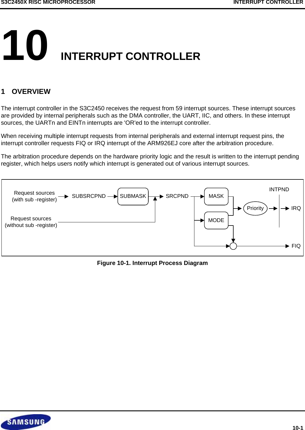
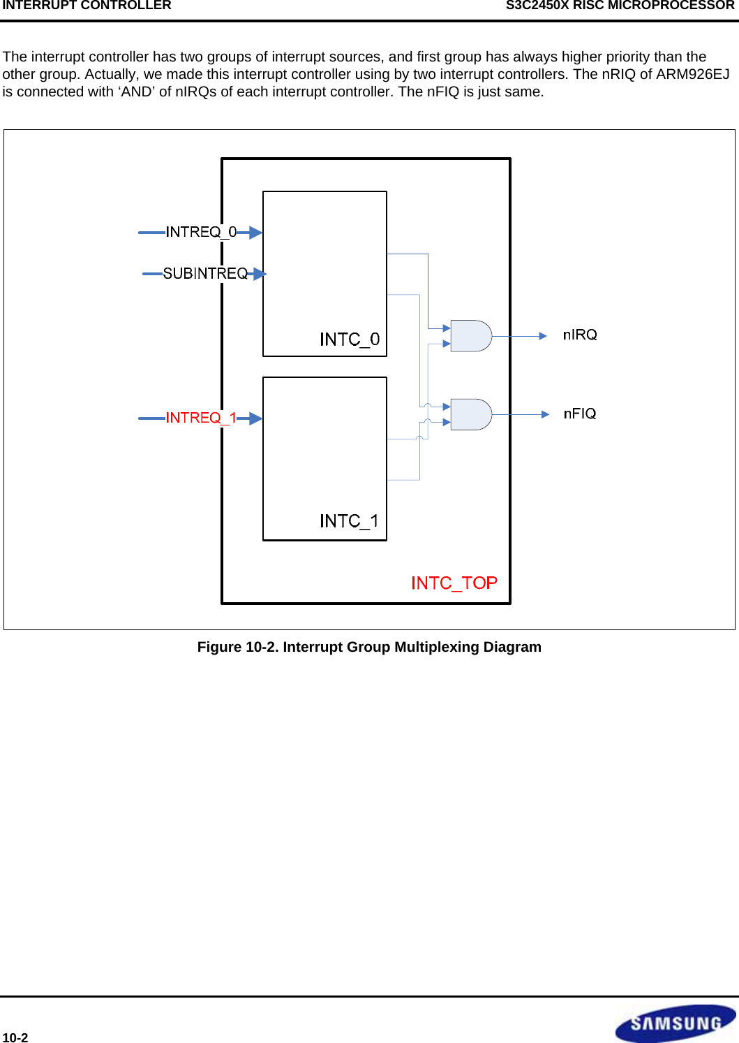
![INTERRUPT CONTROLLER S3C2450X RISC MICROPROCESSOR 10-10 2.1 SOURCE PENDING (SRCPND) REGISTER The SRCPND register is composed of 32 bits each of which is related to an interrupt source. Each bit is set to 1 if the corresponding interrupt source generates the interrupt request and waits for the interrupt to be serviced. Accordingly, this register indicates which interrupt source is waiting for the request to be serviced. Note that each bit of the SRCPND register is automatically set by the interrupt sources regardless of the masking bits in the INTMASK register. In addition, the SRCPND register is not affected by the priority logic of interrupt controller. In the interrupt service routine for a specific interrupt source, the corresponding bit of the SRCPND register has to be cleared to get the interrupt request from the same source correctly. If you return from the ISR without clearing the bit, the interrupt controller operates as if another interrupt request came in from the same source. In other words, if a specific bit of the SRCPND register is set to 1, it is always considered as a valid interrupt request waiting to be serviced. The time to clear the corresponding bit depends on the user's requirement. If you want to receive another valid request from the same source, you should clear the corresponding bit first, and then enable the interrupt. You can clear a specific bit of the SRCPND register by writing a data to this register. It clears only the bit positions of the SRCPND corresponding to those set to one in the data. The bit positions corresponding to those that are set to 0 in the data remains as they are. SOURCE PENDING (SRCPND 1) REGISTER FOR GROUP 1 Register Address R/W Description Reset ValueSRCPND 1 0X4A000000 R/W Indicate the interrupt request status for group 1. 0 = The interrupt has not been requested. 1 = The interrupt source has asserted the interrupt request. 0x00000000SRCPND 2 0X4A000040 R/W Indicate the interrupt request status for group 2.. 0 = The interrupt has not been requested. 1 = The interrupt source has asserted the interrupt request. 0x00000000 SRCPND 1 Bit Description Initial StateINT_ADC [31] 0 = Not requested, 1 = Requested 0 INT_RTC [30] 0 = Not requested, 1 = Requested 0 INT_SPI1 [29] 0 = Not requested, 1 = Requested 0 INT_UART0 [28] 0 = Not requested, 1 = Requested 0 INT_IIC0 [27] 0 = Not requested, 1 = Requested 0 INT_USBH [26] 0 = Not requested, 1 = Requested 0 INT_USBD [25] 0 = Not requested, 1 = Requested 0 INT_NAND [24] 0 = Not requested, 1 = Requested 0 INT_UART1 [23] 0 = Not requested, 1 = Requested 0 INT_SPI0 [22] 0 = Not requested, 1 = Requested 0 INT_SDI0 [21] 0 = Not requested, 1 = Requested 0 INT_SDI1 [20] 0 = Not requested, 1 = Requested 0 INT_CFCON [19] 0 = Not requested, 1 = Requested 0](https://usermanual.wiki/Diasonic-Technology-Co/RVM-704M.Users-Manual/User-Guide-1826140-Page-258.png)
![S3C2450X RISC MICROPROCESSOR INTERRUPT CONTROLLER 10-11 SRCPND 1 Bit Description Initial StateINT_UART3 [18] 0 = Not requested, 1 = Requested 0 INT_DMA [17] 0 = Not requested, 1 = Requested 0 INT_LCD [16] 0 = Not requested, 1 = Requested 0 INT_UART2 [15] 0 = Not requested, 1 = Requested 0 INT_TIMER4 [14] 0 = Not requested, 1 = Requested 0 INT_TIMER3 [13] 0 = Not requested, 1 = Requested 0 INT_TIMER2 [12] 0 = Not requested, 1 = Requested 0 INT_TIMER1 [11] 0 = Not requested, 1 = Requested 0 INT_TIMER0 [10] 0 = Not requested, 1 = Requested 0 INT_WDT/AC97 [9] 0 = Not requested, 1 = Requested 0 INT_TICK [8] 0 = Not requested, 1 = Requested 0 nBATT_FLT [7] 0 = Not requested, 1 = Requested 0 INT_CAM [6] 0 = Not requested, 1 = Requested 0 EINT8_23 [5] 0 = Not requested, 1 = Requested 0 EINT4_7 [4] 0 = Not requested, 1 = Requested 0 EINT3 [3] 0 = Not requested, 1 = Requested 0 EINT2 [2] 0 = Not requested, 1 = Requested 0 EINT1 [1] 0 = Not requested, 1 = Requested 0 EINT0 [0] 0 = Not requested, 1 = Requested 0 SRCPND 2 Bit Description Initial StateINT_I2S1 [7] 0 = Not requested, 1 = Requested 0 INT_I2S0 [6] 0 = Not requested, 1 = Requested 0 INT_PCM1 [5] 0 = Not requested, 1 = Requested 0 INT_PCM0 [4] 0 = Not requested, 1 = Requested 0 Reserved [3] 0 = Not requested, 1 = Requested 0 Reserved [2] 0 = Not requested, 1 = Requested 0 INT_IIC1 [1] 0 = Not requested, 1 = Requested 0 INT_2D [0] 0 = Not requested, 1 = Requested 0](https://usermanual.wiki/Diasonic-Technology-Co/RVM-704M.Users-Manual/User-Guide-1826140-Page-259.png)
![INTERRUPT CONTROLLER S3C2450X RISC MICROPROCESSOR 10-12 2.2 INTERRUPT MODE (INTMOD) REGISTER This register is composed of 32 bits each of which is related to an interrupt source. If a specific bit is set to 1, the corresponding interrupt is processed in the FIQ (fast interrupt) mode. Otherwise, it is processed in the IRQ mode (normal interrupt). Note that only one interrupt source can be serviced in the FIQ mode in the interrupt controller (you should use the FIQ mode only for the urgent interrupt). Thus, only one bit of INTMOD can be set to 1. Register Address R/W Description Reset ValueINTMOD 1 0X4A000004 R/W Interrupt mode regiseter for group 1. 0 = IRQ mode 1 = FIQ mode 0x00000000INTMOD 2 0X4A000044 R/W Interrupt mode regiseter for group 2. 0 = IRQ mode 1 = FIQ mode 0x00000000NOTE: If an interrupt mode is set to FIQ mode in the INTMOD register, FIQ interrupt will not affect both INTPND and INTOFFSET registers. In this case, the two registers are valid only for IRQ mode interrupt source. INTMOD1 Bit Description Initial StateINT_ADC [31] 0 = IRQ, 1 = FIQ 0 INT_RTC [30] 0 = IRQ, 1 = FIQ 0 INT_SPI1 [29] 0 = IRQ, 1 = FIQ 0 INT_UART0 [28] 0 = IRQ, 1 = FIQ 0 INT_IIC0 [27] 0 = IRQ, 1 = FIQ 0 INT_USBH [26] 0 = IRQ, 1 = FIQ 0 INT_USBD [25] 0 = IRQ, 1 = FIQ 0 INT_NAND [24] 0 = IRQ, 1 = FIQ 0 INT_UART1 [23] 0 = IRQ, 1 = FIQ 0 INT_SPI0 [22] 0 = IRQ, 1 = FIQ 0 INT_SDI0 [21] 0 = IRQ, 1 = FIQ 0 INT_SDI1 [20] 0 = IRQ, 1 = FIQ 0 INT_CFCON [19] 0 = IRQ, 1 = FIQ 0 INT_UART3 [18] 0 = IRQ, 1 = FIQ 0 INT_DMA [17] 0 = IRQ, 1 = FIQ 0 INT_LCD [16] 0 = IRQ, 1 = FIQ 0 INT_UART2 [15] 0 = IRQ, 1 = FIQ 0 INT_TIMER4 [14] 0 = IRQ, 1 = FIQ 0 INT_TIMER3 [13] 0 = IRQ, 1 = FIQ 0 INT_TIMER2 [12] 0 = IRQ, 1 = FIQ 0 INT_TIMER1 [11] 0 = IRQ, 1 = FIQ 0 INT_TIMER0 [10] 0 = IRQ, 1 = FIQ 0](https://usermanual.wiki/Diasonic-Technology-Co/RVM-704M.Users-Manual/User-Guide-1826140-Page-260.png)
![S3C2450X RISC MICROPROCESSOR INTERRUPT CONTROLLER 10-13 INTMOD1 Bit Description Initial StateINT_WDT/AC97 [9] 0 = IRQ, 1 = FIQ 0 INT_TICK [8] 0 = IRQ, 1 = FIQ 0 nBATT_FLT [7] 0 = IRQ, 1 = FIQ 0 INT_CAM [6] 0 = IRQ, 1 = FIQ 0 EINT8_23 [5] 0 = IRQ, 1 = FIQ 0 EINT4_7 [4] 0 = IRQ, 1 = FIQ 0 EINT3 [3] 0 = IRQ, 1 = FIQ 0 EINT2 [2] 0 = IRQ, 1 = FIQ 0 EINT1 [1] 0 = IRQ, 1 = FIQ 0 EINT0 [0] 0 = IRQ, 1 = FIQ 0 INTMOD2 Bit Description Initial StateINT_I2S1 [7] 0 = IRQ, 1 = FIQ 0 INT_I2S0 [6] 0 = IRQ, 1 = FIQ 0 INT_PCM1 [5] 0 = IRQ, 1 = FIQ 0 INT_PCM0 [4] 0 = IRQ, 1 = FIQ 0 Reserved [3] 0 = IRQ, 1 = FIQ 0 Reserved [2] 0 = IRQ, 1 = FIQ 0 INT_IIC1 [1] 0 = IRQ, 1 = FIQ 0 INT_2D [0] 0 = IRQ, 1 = FIQ 0](https://usermanual.wiki/Diasonic-Technology-Co/RVM-704M.Users-Manual/User-Guide-1826140-Page-261.png)
![INTERRUPT CONTROLLER S3C2450X RISC MICROPROCESSOR 10-14 2.3 INTERRUPT MASK (INTMSK) REGISTER This register also has 32 bits each of which is related to an interrupt source. If a specific bit is set to 1, the CPU does not service the interrupt request from the corresponding interrupt source (note that even in such a case, the corresponding bit of SRCPND register is set to 1). If the mask bit is 0, the interrupt request can be serviced. Register Address R/W Description Reset ValueINTMSK1 0X4A000008 R/W Determine which interrupt source of group 1is masked. The masked interrupt source will not be serviced. 0 = Interrupt service is available. 1 = Interrupt service is masked. 0xFFFFFFFFINTMSK2 0X4A000048 R/W Determine which interrupt source of group 2 is masked. The masked interrupt source will not be serviced. 0 = Interrupt service is available. 1 = Interrupt service is masked. 0xFFFFFFFF INTMSK1 Bit Description Initial StateINT_ADC [31] 0 = Service available, 1 = Masked 1 INT_RTC [30] 0 = Service available, 1 = Masked 1 INT_SPI1 [29] 0 = Service available, 1 = Masked 1 INT_UART0 [28] 0 = Service available, 1 = Masked 1 INT_IIC0 [27] 0 = Service available, 1 = Masked 1 INT_USBH [26] 0 = Service available, 1 = Masked 1 INT_USBD [25] 0 = Service available, 1 = Masked 1 INT_NAND [24] 0 = Service available, 1 = Masked 1 INT_UART1 [23] 0 = Service available, 1 = Masked 1 INT_SPI0 [22] 0 = Service available, 1 = Masked 1 INT_SDI0 [21] 0 = Service available, 1 = Masked 1 INT_SDI1 [20] 0 = Service available, 1 = Masked 1 INT_CFCON [19] 0 = Service available, 1 = Masked 1 INT_UART3 [18] 0 = Service available, 1 = Masked 1 INT_DMA [17] 0 = Service available, 1 = Masked 1 INT_LCD [16] 0 = Service available, 1 = Masked 1 INT_UART2 [15] 0 = Service available, 1 = Masked 1 INT_TIMER4 [14] 0 = Service available, 1 = Masked 1 INT_TIMER3 [13] 0 = Service available, 1 = Masked 1 INT_TIMER2 [12] 0 = Service available, 1 = Masked 1 INT_TIMER1 [11] 0 = Service available, 1 = Masked 1 INT_TIMER0 [10] 0 = Service available, 1 = Masked 1 INT_WDT/AC97 [9] 0 = Service available, 1 = Masked 1](https://usermanual.wiki/Diasonic-Technology-Co/RVM-704M.Users-Manual/User-Guide-1826140-Page-262.png)
![S3C2450X RISC MICROPROCESSOR INTERRUPT CONTROLLER 10-15 INTMSK1 Bit Description Initial StateINT_TICK [8] 0 = Service available, 1 = Masked 1 nBATT_FLT [7] 0 = Service available, 1 = Masked 1 INT_CAM [6] 0 = Service available, 1 = Masked 1 EINT8_23 [5] 0 = Service available, 1 = Masked 1 EINT4_7 [4] 0 = Service available, 1 = Masked 1 EINT3 [3] 0 = Service available, 1 = Masked 1 EINT2 [2] 0 = Service available, 1 = Masked 1 EINT1 [1] 0 = Service available, 1 = Masked 1 EINT0 [0] 0 = Service available, 1 = Masked 1 INTMSK2 Bit Description Initial StateINT_I2S1 [7] 0 = Service available, 1 = Masked 1 INT_I2S0 [6] 0 = Service available, 1 = Masked 1 INT_PCM1 [5] 0 = Service available, 1 = Masked 1 INT_PCM0 [4] 0 = Service available, 1 = Masked 1 Reserved [3] 0 = Service available, 1 = Masked 1 Reserved [2] 0 = Service available, 1 = Masked 1 INT_IIC1 [1] 0 = Service available, 1 = Masked 1 INT_2D [0] 0 = Service available, 1 = Masked 1](https://usermanual.wiki/Diasonic-Technology-Co/RVM-704M.Users-Manual/User-Guide-1826140-Page-263.png)
![INTERRUPT CONTROLLER S3C2450X RISC MICROPROCESSOR 10-16 2.4 INTERRUPT PENDING (INTPND) REGISTER Each of the 32 bits in the interrupt pending register shows whether the corresponding interrupt request, which is unmasked and waits for the interrupt to be serviced, has the highest priority. Since the INTPND register is located after the priority logic, only one bit can be set to 1, and that interrupt request generates IRQ to CPU. In interrupt service routine for IRQ, you can read this register to determine which interrupt source is serviced among the 32 sources. Like the SRCPND register, this register has to be cleared in the interrupt service routine after clearing the SRCPND register. We can clear a specific bit of the INTPND register by writing a data to this register. It clears only the bit positions of the INTPND register corresponding to those set to one in the data. The bit positions corresponding to those that are set to 0 in the data remains as they are. Register Address R/W Description Reset ValueINTPND1 0X4A000010 R/W Indicate the interrupt request status for group 1. 0 = The interrupt has not been requested. 1 = The interrupt source has asserted the interrupt request. 0x00000000INTPND2 0X4A000050 R/W Indicate the interrupt request status for group 2. 0 = The interrupt has not been requested. 1 = The interrupt source has asserted the interrupt request. 0x00000000NOTES: 1. If the FIQ mode interrupt occurs, the corresponding bit of INTPND will not be turned on as the INTPND register is available only for IRQ mode interrupt. 2. Cautions in clearing the INTPND register. The INTPND register is cleared to "0" by writing "1". If the INTPND bit, which has "1", is cleared by "0", the INTPND register & INTOFFSET register may have unexpected value in some case. So, you never write "0" on the INTPND bit having "1". The convenient method to clear the INTPND register is writing the INTPND register value on the INTPND register. (In even our example code, this guide hasn't been applied yet.) INTPND1 Bit Description Initial StateINT_ADC [31] 0 = Not requested, 1 = Requested 0 INT_RTC [30] 0 = Not requested, 1 = Requested 0 INT_SPI1 [29] 0 = Not requested, 1 = Requested 0 INT_UART0 [28] 0 = Not requested, 1 = Requested 0 INT_IIC0 [27] 0 = Not requested, 1 = Requested 0 INT_USBH [26] 0 = Not requested, 1 = Requested 0 INT_USBD [25] 0 = Not requested, 1 = Requested 0 INT_NAND [24] 0 = Not requested, 1 = Requested 0 INT_UART1 [23] 0 = Not requested, 1 = Requested 0 INT_SPI0 [22] 0 = Not requested, 1 = Requested 0 INT_SDI0 [21] 0 = Not requested, 1 = Requested 0 INT_SDI1 [20] 0 = Not requested, 1 = Requested 0 INT_CFCON [19] 0 = Not requested, 1 = Requested 0](https://usermanual.wiki/Diasonic-Technology-Co/RVM-704M.Users-Manual/User-Guide-1826140-Page-264.png)
![S3C2450X RISC MICROPROCESSOR INTERRUPT CONTROLLER 10-17 INTPND1 Bit Description Initial StateINT_UART3 [18] 0 = Not requested, 1 = Requested 0 INT_DMA [17] 0 = Not requested, 1 = Requested 0 INT_LCD [16] 0 = Not requested, 1 = Requested 0 INT_UART2 [15] 0 = Not requested, 1 = Requested 0 INT_TIMER4 [14] 0 = Not requested, 1 = Requested 0 INT_TIMER3 [13] 0 = Not requested, 1 = Requested 0 INT_TIMER2 [12] 0 = Not requested, 1 = Requested 0 INT_TIMER1 [11] 0 = Not requested, 1 = Requested 0 INT_TIMER0 [10] 0 = Not requested, 1 = Requested 0 INT_WDT/AC97 [9] 0 = Not requested, 1 = Requested 0 INT_TICK [8] 0 = Not requested, 1 = Requested 0 nBATT_FLT [7] 0 = Not requested, 1 = Requested 0 INT_CAM [6] 0 = Not requested, 1 = Requested 0 EINT8_23 [5] 0 = Not requested, 1 = Requested 0 EINT4_7 [4] 0 = Not requested, 1 = Requested 0 EINT3 [3] 0 = Not requested, 1 = Requested 0 EINT2 [2] 0 = Not requested, 1 = Requested 0 EINT1 [1] 0 = Not requested, 1 = Requested 0 EINT0 [0] 0 = Not requested, 1 = Requested 0 INT_I2S1 [7] 0 = Not requested, 1 = Requested 0 INT_I2S0 [6] 0 = Not requested, 1 = Requested 0 INT_PCM1 [5] 0 = Not requested, 1 = Requested 0 INT_PCM0 [4] 0 = Not requested, 1 = Requested 0 Reserved [3] 0 = Not requested, 1 = Requested 0 Reserved [2] 0 = Not requested, 1 = Requested 0 INT_IIC1 [1] 0 = Not requested, 1 = Requested 0 INT_2D [0] 0 = Not requested, 1 = Requested 0](https://usermanual.wiki/Diasonic-Technology-Co/RVM-704M.Users-Manual/User-Guide-1826140-Page-265.png)
![INTERRUPT CONTROLLER S3C2450X RISC MICROPROCESSOR 10-20 2.6 SUB SOURCE PENDING (SUBSRCPND) REGISTER You can clear a specific bit of the SUBSRCPND register by writing a data to this register. It clears only the bit positions of the SUBSRCPND register corresponding to those set to one in the data. The bit positions corresponding to those that are set to 0 in the data remains as they are. Register Address R/W Description Reset ValueSUBSRCPND 0X4A000018 R/W Indicate the interrupt request status. 0 = The interrupt has not been requested. 1 = The interrupt source has asserted the interrupt request. 0x00000000 SUBSRCPND Bit Description SRCPND Initial StateReserved [31] Not used 0 SUBINT_DMA7 [30] 0 = Not requested, 1 = Requested 0 SUBINT_DMA6 [29] 0 = Not requested, 1 = Requested INT_DMA 0 SUBINT_AC97 [28] 0 = Not requested, 1 = Requested 0 SUBINT_WDT [27] 0 = Not requested, 1 = Requested INT_WDT_AC97 0 SUBINT_ERR3 [26] 0 = Not requested, 1 = Requested 0 SUBINT_TXD3 [25] 0 = Not requested, 1 = Requested 0 SUBINT_RXD3 [24] 0 = Not requested, 1 = Requested INT_UART3 0 SUBINT_DMA5 [23] 0 = Not requested, 1 = Requested 0 SUBINT_DMA4 [22] 0 = Not requested, 1 = Requested 0 SUBINT_DMA3 [21] 0 = Not requested, 1 = Requested 0 SUBINT_DMA2 [20] 0 = Not requested, 1 = Requested 0 SUBINT_DMA1 [19] 0 = Not requested, 1 = Requested 0 SUBINT_DMA0 [18] 0 = Not requested, 1 = Requested INT_DMA 0 SUBINT_LCD4 (i80 I/F) [17] 0 = Not requested, 1 = Requested 0 SUBINT_LCD3 (LCD Frame) [16] 0 = Not requested, 1 = Requested 0 SUBINT_LCD2 (LCD FIFO) [15] 0 = Not requested, 1 = Requested 0 Reserved [14] Not used INT_LCD 0 Reserved [13] Reserved for future usage Reserved 0 SUBINT_CAM_P [12] 0 = Not requested, 1 = Requested 0 SUBINT_CAM_C [11] 0 = Not requested, 1 = Requested INT_CAM 0 SUBINT_ADC [10] 0 = Not requested, 1 = Requested 0 SUBINT_TC [9] 0 = Not requested, 1 = Requested INT_ADC 0 SUBINT_ERR2 [8] 0 = Not requested, 1 = Requested 0 SUBINT_TXD2 [7] 0 = Not requested, 1 = Requested 0 SUBINT_RXD2 [6] 0 = Not requested, 1 = Requested INT_UART2 0](https://usermanual.wiki/Diasonic-Technology-Co/RVM-704M.Users-Manual/User-Guide-1826140-Page-268.png)
![S3C2450X RISC MICROPROCESSOR INTERRUPT CONTROLLER 10-21 SUBSRCPND Bit Description SRCPND Initial StateSUBINT_ERR1 [5] 0 = Not requested, 1 = Requested 0 SUBINT_TXD1 [4] 0 = Not requested, 1 = Requested 0 SUBINT_RXD1 [3] 0 = Not requested, 1 = Requested INT_UART1 0 SUBINT_ERR0 [2] 0 = Not requested, 1 = Requested 0 SUBINT_TXD0 [1] 0 = Not requested, 1 = Requested 0 SUBINT_RXD0 [0] 0 = Not requested, 1 = Requested INT_UART0 0](https://usermanual.wiki/Diasonic-Technology-Co/RVM-704M.Users-Manual/User-Guide-1826140-Page-269.png)
![INTERRUPT CONTROLLER S3C2450X RISC MICROPROCESSOR 10-22 2.7 INTERRUPT SUB MASK (INTSUBMSK) REGISTER This register has 27 bits each of which is related to an interrupt source. If a specific bit is set to 1, the interrupt request from the corresponding interrupt source is not serviced by the CPU (note that even in such a case, the corresponding bit of the SUBSRCPND register is set to 1). If the mask bit is 0, the interrupt request can be serviced. Register Address R/W Description Reset ValueINTSUBMSK 0X4A00001C R/W Determine which interrupt source is masked. The masked interrupt source will not be serviced. 0 = Interrupt service is available. 1 = Interrupt service is masked. 0xFFFFFFFF INTSUBMASK Bit Description INTMASK Initial StateReserved [31] Not used 1 SUBINT_DMA7 [30] 0 = Service available, 1 = Masked SUBINT_DMA6 [29] 0 = Service available, 1 = Masked INT_DMA SUBINT_AC97 [28] 0 = Service available, 1 = Masked 1 SUBINT_WDT [27] 0 = Service available, 1 = Masked INT_WDT_AC97 1 SUBINT_ERR3 [26] 0 = Service available, 1 = Masked 1 SUBINT_TXD3 [25] 0 = Service available, 1 = Masked 1 SUBINT_RXD3 [24] 0 = Service available, 1 = Masked INT_UART3 1 SUBINT_DMA5 [23] 0 = Service available, 1 = Masked 1 SUBINT_DMA4 [22] 0 = Service available, 1 = Masked 1 SUBINT_DMA3 [21] 0 = Service available, 1 = Masked 1 SUBINT_DMA2 [20] 0 = Service available, 1 = Masked 1 SUBINT_DMA1 [19] 0 = Service available, 1 = Masked 1 SUBINT_DMA0 [18] 0 = Service available, 1 = Masked INT_DMA 1 SUBINT_LCD4 (i80 I/F) [17] 0 = Service available, 1 = Masked 1 SUBINT_LCD3 (LCD Frame) [16] 0 = Service available, 1 = Masked 1 SUBINT_LCD2 (LCD FIFO) [15] 0 = Service available, 1 = Masked 1 Reserved [14] Not used INT_LCD 1 Reserved [13] Reserved for future usage Reserved 1 SUBINT_CAM_P [12] 0 = Service available, 1 = Masked 1 SUBINT_CAM_C [11] 0 = Service available, 1 = Masked INT_CAM 1 SUBINT_ADC [10] 0 = Service available, 1 = Masked 1 SUBINT_TC [9] 0 = Service available, 1 = Masked INT_ADC 1 SUBINT_ERR2 [8] 0 = Service available, 1 = Masked 1 SUBINT_TXD2 [7] 0 = Service available, 1 = Masked INT_UART2 1](https://usermanual.wiki/Diasonic-Technology-Co/RVM-704M.Users-Manual/User-Guide-1826140-Page-270.png)
![S3C2450X RISC MICROPROCESSOR INTERRUPT CONTROLLER 10-23 INTSUBMASK Bit Description INTMASK Initial StateSUBINT_RXD2 [6] 0 = Service available, 1 = Masked 1 SUBINT_ERR1 [5] 0 = Service available, 1 = Masked 1 SUBINT_TXD1 [4] 0 = Service available, 1 = Masked 1 SUBINT_RXD1 [3] 0 = Service available, 1 = Masked INT_UART1 1 SUBINT_ERR0 [2] 0 = Service available, 1 = Masked 1 SUBINT_TXD0 [1] 0 = Service available, 1 = Masked 1 SUBINT_RXD0 [0] 0 = Service available, 1 = Masked INT_UART0 1](https://usermanual.wiki/Diasonic-Technology-Co/RVM-704M.Users-Manual/User-Guide-1826140-Page-271.png)
![INTERRUPT CONTROLLER S3C2450X RISC MICROPROCESSOR 10-24 2.8 PRIORITY MODE REGISTER (PRIORITY_MODE) Register Address R/W Description Reset ValuePRIORITY_MODE1 0x4A000030 R/W IRQ priority mode register 0x00000000PRIORITY_MODE2 0x4A000070 R/W IRQ priority mode register 0x00000000 PRIORITY_MODE1 Bit Description Initial StateARB_MODE6 [27] Arbiter 6 group priority mode selection 0 = Fixed ends & Rotate middle 1 = Rotate all 0 ARB_SEL6 [26:24] Arbiter 6 group priority order set 1) ARB_MODE6 = 1’b0 00 = REQ 0-1-2-3-4-5 01 = REQ 0-2-3-4-1-5 10 = REQ 0-3-4-1-2-5 11 = REQ 0-4-1-2-3-5 2) ARB_MODE6 = 1’b1 000 = REQ 0-1-2-3-4-5 001 = REQ 1-2-3-4-5-0 010 = REQ 2-3-4-5-0-1 011 = REQ 3-4-5-0-1-2 100 = REQ 4-5-0-1-2-3 101 = REQ 5-0-1-2-3-4 0 ARB_MODE5 [23] Arbiter 5 group priority mode selection 0 = Fixed ends & Rotate middle 0 ARB_SEL5 [22:20] Arbiter 5 group priority order set 1) ARB_MODE5 = 1’b0 00 = REQ 0-1-2-3-4-5 01 = REQ 0-2-3-4-1-5 10 = REQ 0-3-4-1-2-5 11 = REQ 0-4-1-2-3-5 0 ARB_MODE4 [19] Arbiter 4 group priority mode selection 0 = Fixed ends & Rotate middle 1 = Rotate all 0 ARB_SEL4 [18:16] Arbiter 4 group priority order set 1) ARB_MODE4 = 1’b0 00 = REQ 0-1-2-3-4-5 01 = REQ 0-2-3-4-1-5 10 = REQ 0-3-4-1-2-5 11 = REQ 0-4-1-2-3-5 2) ARB_MODE4 = 1’b1 000 = REQ 0-1-2-3-4-5 001 = REQ 1-2-3-4-5-0 010 = REQ 2-3-4-5-0-1 011 = REQ 3-4-5-0-1-2 100 = REQ 4-5-0-1-2-3 101 = REQ 5-0-1-2-3-4 0](https://usermanual.wiki/Diasonic-Technology-Co/RVM-704M.Users-Manual/User-Guide-1826140-Page-272.png)
![S3C2450X RISC MICROPROCESSOR INTERRUPT CONTROLLER 10-25 PRIORITY_MODE1 Bit Description Initial StateARB_MODE3 [15] Arbiter 3 group priority mode selection 0 = Fixed ends & Rotate middle 1 = Rotate all 0 ARB_SEL3 [14:12] Arbiter 3 group priority order set 1) ARB_MODE3 = 1’b0 00 = REQ 0-1-2-3-4-5 01 = REQ 0-2-3-4-1-5 10 = REQ 0-3-4-1-2-5 11 = REQ 0-4-1-2-3-5 2) ARB_MODE3 = 1’b1 000 = REQ 0-1-2-3-4-5 001 = REQ 1-2-3-4-5-0 010 = REQ 2-3-4-5-0-1 011 = REQ 3-4-5-0-1-2 100 = REQ 4-5-0-1-2-3 101 = REQ 5-0-1-2-3-4 0 ARB_MODE2 [11] Arbiter 2 group priority mode selection 0 = Fixed ends & Rotate middle 1 = Rotate all 0 ARB_SEL2 [10:8] Arbiter 2 group priority order set 1) ARB_MODE2 = 1’b0 00 = REQ 0-1-2-3-4-5 01 = REQ 0-2-3-4-1-5 10 = REQ 0-3-4-1-2-5 11 = REQ 0-4-1-2-3-5 2) ARB_MODE2 = 1’b1 000 = REQ 0-1-2-3-4-5 001 = REQ 1-2-3-4-5-0 010 = REQ 2-3-4-5-0-1 011 = REQ 3-4-5-0-1-2 100 = REQ 4-5-0-1-2-3 101 = REQ 5-0-1-2-3-4 0 ARB_MODE1 [7] Arbiter 1 group priority mode selection 0 = Fixed ends & Rotate middle 1 = Rotate all 0 ARB_SEL1 [6:4] Arbiter 1 group priority order set 1) ARB_MODE1 = 1’b0 00 = REQ 0-1-2-3-4-5 01 = REQ 0-2-3-4-1-5 10 = REQ 0-3-4-1-2-5 11 = REQ 0-4-1-2-3-5 2) ARB_MODE1 = 1’b1 000 = REQ 0-1-2-3-4-5 001 = REQ 1-2-3-4-5-0 010 = REQ 2-3-4-5-0-1 011 = REQ 3-4-5-0-1-2 100 = REQ 4-5-0-1-2-3 0](https://usermanual.wiki/Diasonic-Technology-Co/RVM-704M.Users-Manual/User-Guide-1826140-Page-273.png)
![INTERRUPT CONTROLLER S3C2450X RISC MICROPROCESSOR 10-26 PRIORITY_MODE1 Bit Description Initial State101 = REQ 5-0-1-2-3-4 ARB_MODE0 [3] Arbiter 0 group priority mode selection 0 = Fixed ends & Rotate middle 0 ARB_SEL0 [2:0] Arbiter 0 group priority order set 1) ARB_MODE0 = 1’b0 00 = REQ 0-1-2-3-4-5 01 = REQ 0-2-3-4-1-5 10 = REQ 0-3-4-1-2-5 11 = REQ 0-4-1-2-3-5 0](https://usermanual.wiki/Diasonic-Technology-Co/RVM-704M.Users-Manual/User-Guide-1826140-Page-274.png)
![S3C2450X RISC MICROPROCESSOR INTERRUPT CONTROLLER 10-27 PRIORITY_MODE2 Bit Description Initial StateARB_MODE13 [27] Arbiter 13 group priority mode selection 0 = Fixed ends & Rotate middle 1 = Rotate all 0 ARB_SEL13 [26:24] Arbiter 13 group priority order set 1) ARB_MODE13 = 1’b0 00 = REQ 0-1-2-3-4-5 01 = REQ 0-2-3-4-1-5 10 = REQ 0-3-4-1-2-5 11 = REQ 0-4-1-2-3-5 2) ARB_MODE13 = 1’b1 000 = REQ 0-1-2-3-4-5 001 = REQ 1-2-3-4-5-0 010 = REQ 2-3-4-5-0-1 011 = REQ 3-4-5-0-1-2 100 = REQ 4-5-0-1-2-3 101 = REQ 5-0-1-2-3-4 0 ARB_MODE12 [23] Arbiter 12 group priority mode selection 0 = Fixed ends & Rotate middle 0 ARB_SEL12 [22:20] Arbiter 12 group priority order set 1) ARB_MODE12 = 1’b0 00 = REQ 0-1-2-3-4-5 01 = REQ 0-2-3-4-1-5 10 = REQ 0-3-4-1-2-5 11 = REQ 0-4-1-2-3-5 0 ARB_MODE11 [19] Arbiter 11 group priority mode selection 0 = Fixed ends & Rotate middle 1 = Rotate all 0 ARB_SEL11 [18:16] Arbiter 11 group priority order set 1) ARB_MODE11 = 1’b0 00 = REQ 0-1-2-3-4-5 01 = REQ 0-2-3-4-1-5 10 = REQ 0-3-4-1-2-5 11 = REQ 0-4-1-2-3-5 2) ARB_MODE11 = 1’b1 000 = REQ 0-1-2-3-4-5 001 = REQ 1-2-3-4-5-0 010 = REQ 2-3-4-5-0-1 011 = REQ 3-4-5-0-1-2 100 = REQ 4-5-0-1-2-3 101 = REQ 5-0-1-2-3-4 0 ARB_MODE10 [15] Arbiter 10 group priority mode selection 0 = Fixed ends & Rotate middle 1 = Rotate all 0 ARB_SEL10 [14:12] Arbiter 10 group priority order set 0](https://usermanual.wiki/Diasonic-Technology-Co/RVM-704M.Users-Manual/User-Guide-1826140-Page-275.png)
![INTERRUPT CONTROLLER S3C2450X RISC MICROPROCESSOR 10-28 PRIORITY_MODE2 Bit Description Initial State1) ARB_MODE10 = 1’b0 00 = REQ 0-1-2-3-4-5 01 = REQ 0-2-3-4-1-5 10 = REQ 0-3-4-1-2-5 11 = REQ 0-4-1-2-3-5 2) ARB_MODE10 = 1’b1 000 = REQ 0-1-2-3-4-5 001 = REQ 1-2-3-4-5-0 010 = REQ 2-3-4-5-0-1 011 = REQ 3-4-5-0-1-2 100 = REQ 4-5-0-1-2-3 101 = REQ 5-0-1-2-3-4 ARB_MODE9 [11] Arbiter 9 group priority mode selection 0 = Fixed ends & Rotate middle 1 = Rotate all 0 ARB_SEL9 [10:8] Arbiter 9 group priority order set 1) ARB_MODE9 = 1’b0 00 = REQ 0-1-2-3-4-5 01 = REQ 0-2-3-4-1-5 10 = REQ 0-3-4-1-2-5 11 = REQ 0-4-1-2-3-5 2) ARB_MODE9 = 1’b1 000 = REQ 0-1-2-3-4-5 001 = REQ 1-2-3-4-5-0 010 = REQ 2-3-4-5-0-1 011 = REQ 3-4-5-0-1-2 100 = REQ 4-5-0-1-2-3 101 = REQ 5-0-1-2-3-4 0 ARB_MODE8 [7] Arbiter 8 group priority mode selection 0 = Fixed ends & Rotate middle 1 = Rotate all 0 ARB_SEL8 [6:4] Arbiter 8 group priority order set 1) ARB_MODE8 = 1’b0 00 = REQ 0-1-2-3-4-5 01 = REQ 0-2-3-4-1-5 10 = REQ 0-3-4-1-2-5 11 = REQ 0-4-1-2-3-5 2) ARB_MODE8 = 1’b1 000 = REQ 0-1-2-3-4-5 001 = REQ 1-2-3-4-5-0 010 = REQ 2-3-4-5-0-1 011 = REQ 3-4-5-0-1-2 100 = REQ 4-5-0-1-2-3 101 = REQ 5-0-1-2-3-4 0 ARB_MODE7 [3] Arbiter 7 group priority mode selection 0 = Fixed ends & Rotate middle 0](https://usermanual.wiki/Diasonic-Technology-Co/RVM-704M.Users-Manual/User-Guide-1826140-Page-276.png)
![S3C2450X RISC MICROPROCESSOR INTERRUPT CONTROLLER 10-29 PRIORITY_MODE2 Bit Description Initial StateARB_SEL7 [2:0] Arbiter 7 group priority order set 1) ARB_MODE7 = 1’b0 00 = REQ 0-1-2-3-4-5 01 = REQ 0-2-3-4-1-5 10 = REQ 0-3-4-1-2-5 11 = REQ 0-4-1-2-3-5 0 2.9 PRIORITY UPDATE REGISTER (PRIORITY_UPDATE) Register Address R/W Description Reset ValuePRIORITY_ UPDATE1 0x4A000034 R/W IRQ priority update register 0x7F PRIORITY_ UPDATE2 0x4A000074 R/W IRQ priority update register 0x7F PRIORITY_UPDATE1 Bit Description Initial StateARB_UPDATE6 [6] Arbiter 6 group priority rotate enable 0 = Priority does not rotate 1 = Priority rotate enable 1 ARB_UPDATE5 [5] Arbiter 5 group priority rotate enable 0 = Priority does not rotate 1 = Priority rotate enable 1 ARB_UPDATE4 [4] Arbiter 4 group priority rotate enable 0 = Priority does not rotate 1 = Priority rotate enable 1 ARB_UPDATE3 [3] Arbiter 3 group priority rotate enable 0 = Priority does not rotate 1 = Priority rotate enable 1 ARB_UPDATE2 [2] Arbiter 2 group priority rotate enable 0 = Priority does not rotate 1 = Priority rotate enable 1 ARB_UPDATE1 [1] Arbiter 1 group priority rotate enable 0 = Priority does not rotate 1 = Priority rotate enable 1 ARB_UPDATE0 [0] Arbiter 0 group priority rotate enable 0 = Priority does not rotate 1 = Priority rotate enable 1](https://usermanual.wiki/Diasonic-Technology-Co/RVM-704M.Users-Manual/User-Guide-1826140-Page-277.png)
![INTERRUPT CONTROLLER S3C2450X RISC MICROPROCESSOR 10-30 PRIORITY_UPDATE2 Bit Description Initial StateARB_UPDATE13 [6] Arbiter 13 group priority rotate enable 0 = Priority does not rotate 1 = Priority rotate enable 1 ARB_UPDATE12 [5] Arbiter 12 group priority rotate enable 0 = Priority does not rotate 1 = Priority rotate enable 1 ARB_UPDATE11 [4] Arbiter 11 group priority rotate enable 0 = Priority does not rotate 1 = Priority rotate enable 1 ARB_UPDATE10 [3] Arbiter 10 group priority rotate enable 0 = Priority does not rotate 1 = Priority rotate enable 1 ARB_UPDATE9 [2] Arbiter 9 group priority rotate enable 0 = Priority does not rotate 1 = Priority rotate enable 1 ARB_UPDATE8 [1] Arbiter 8 group priority rotate enable 0 = Priority does not rotate 1 = Priority rotate enable 1 ARB_UPDATE7 [0] Arbiter 7 group priority rotate enable 0 = Priority does not rotate 1 = Priority rotate enable 1](https://usermanual.wiki/Diasonic-Technology-Co/RVM-704M.Users-Manual/User-Guide-1826140-Page-278.png)
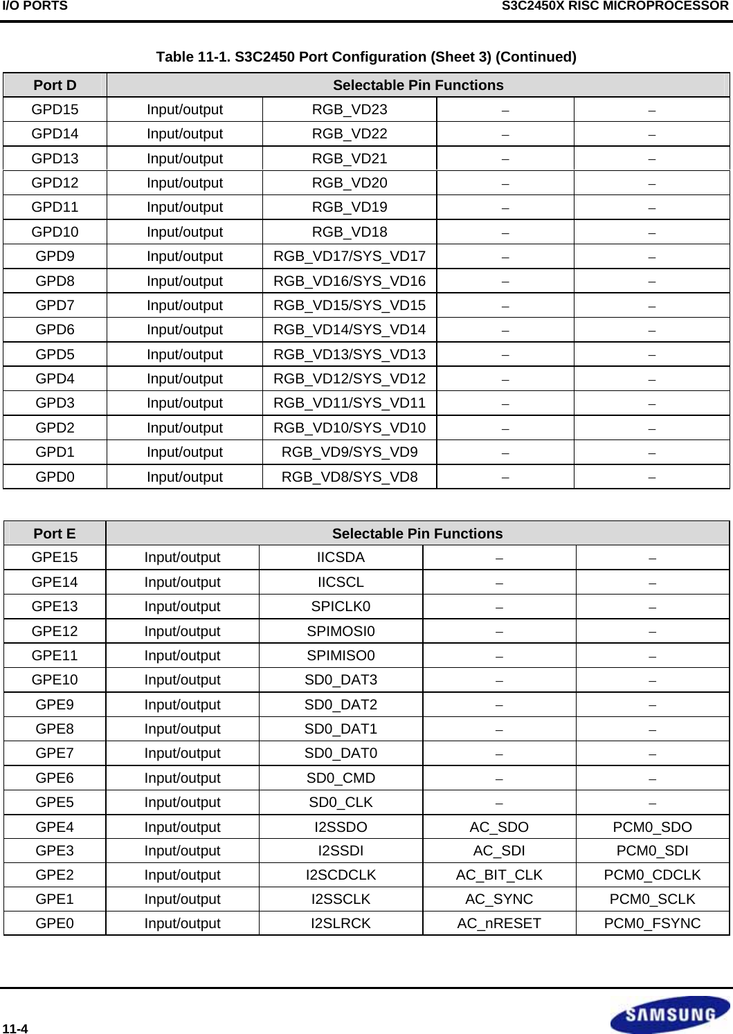
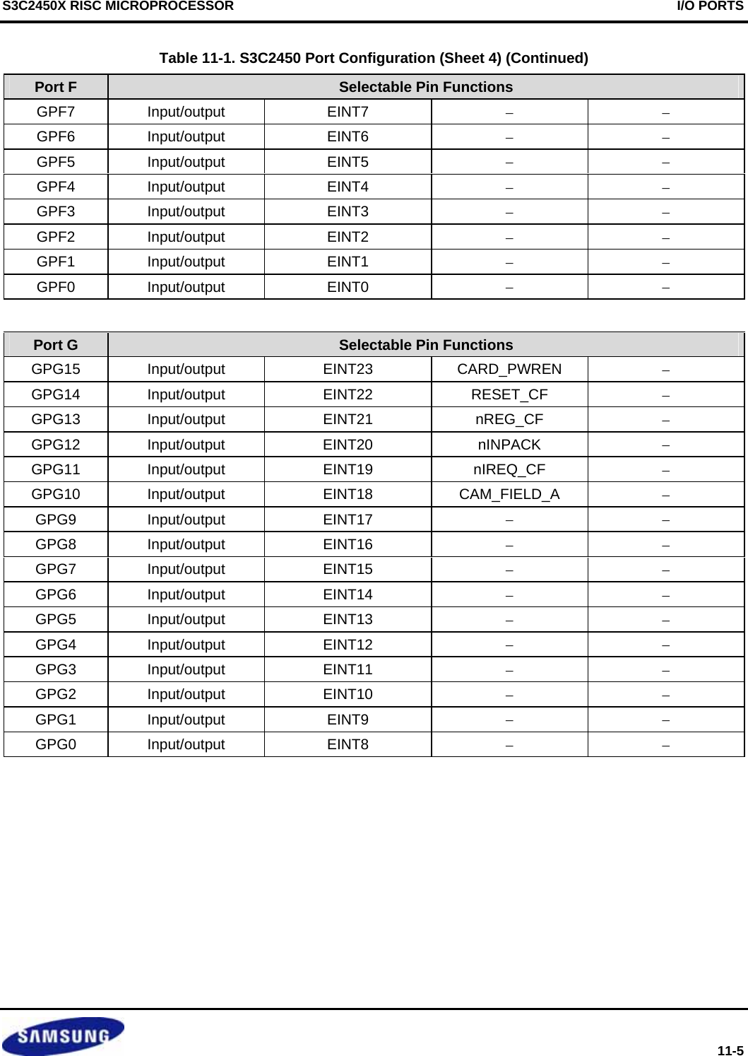
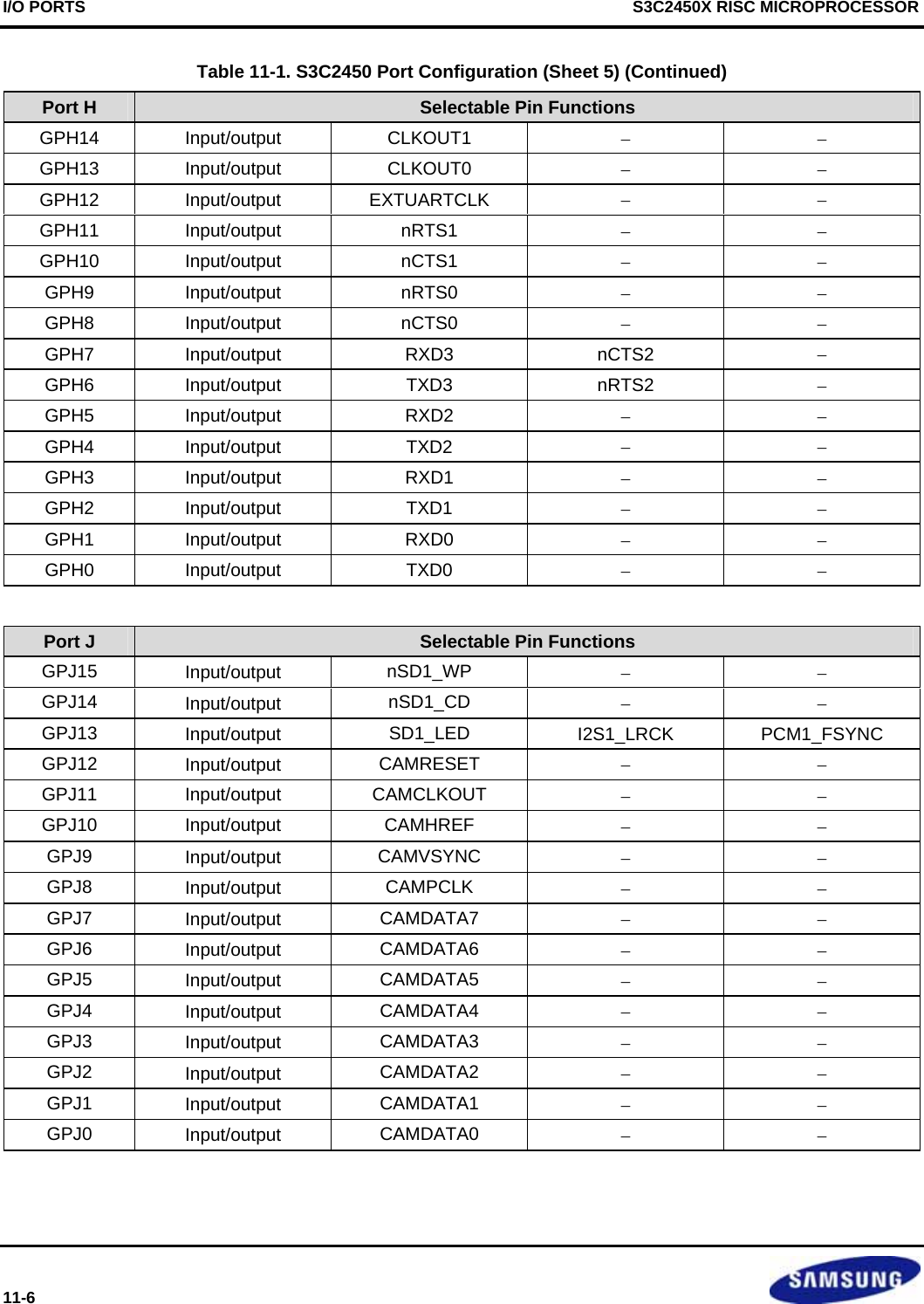
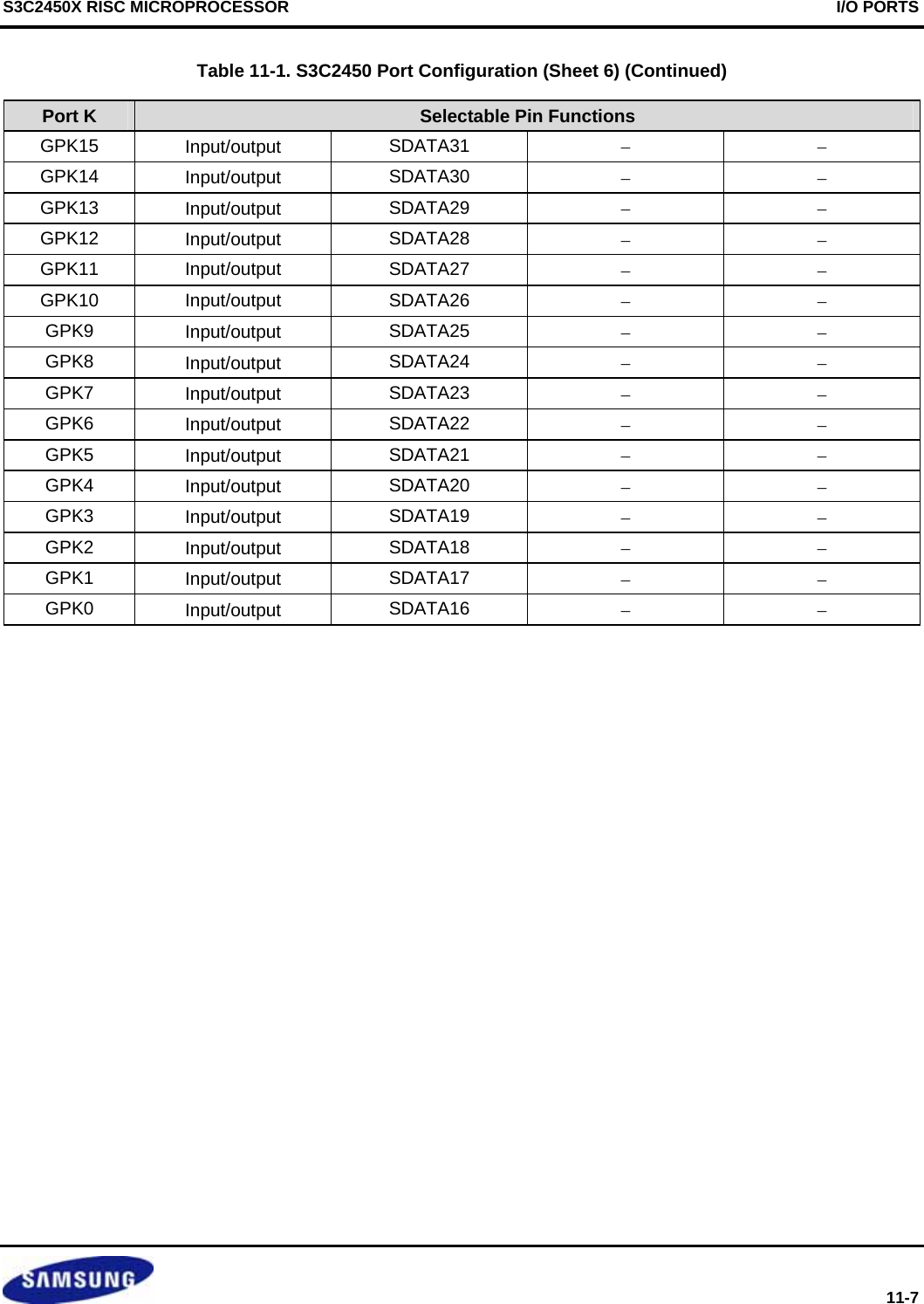
![S3C2450X RISC MICROPROCESSOR I/O PORTS 11-9 2 PORT CONTROL DESCRIPTIONS 2.1 PORT CONFIGURATION REGISTER (GPACON-GPMCON) In S3C2450, most of the pins are multiplexed pins. So, It is determined which function is selected for each pins. The GPxCON(port control register) determines which function is used for each pin. If GPF0 – GPF7, GPG0 – GPG7 is used for the wakeup signal in Sleep/Stop/DeepStop mode, these ports must be configured in EINT. 2.2 PORT DATA REGISTER (GPADAT-GPMDAT) If ports are configured as output ports, data can be written to the corresponding bit of GPxDAT. If Ports are configured as input ports, the data can be read from the corresponding bit of GPxDAT. 2.3 PORT PULL-UP/DOWN REGISTER (GPBUDP-GPMUDP) The port pull-up/down register controls the pull-up/down resister enable/disable of each port group. When the corresponding bit is 0, the pull-down resister of the pin is enabled. When 1, the pull-down resister is disabled. If the port pull-down register is enabled then the pull-down resisters work without pin’s functional setting(input, output, DATAn, EINTn and etc) 2.4 MISCELLANEOUS CONTROL REGISTER This register controls mode selection, and CLKOUT selection. 2.5 EXTERNAL INTERRUPT CONTROL REGISTER The 24 external interrupts are requested by various signaling methods. The EXTINT register configures the signaling method among the low level trigger, high level trigger, falling edge trigger, rising edge trigger, and both edge trigger for the external interrupt request Because each external interrupt pin has a digital filter, the interrupt controller can recognize the request signal that is longer than 3 clocks. EINT[15:0] are used for wakeup sources from Sleep/Stop/DeepStop mode. Caution I/O ports In VDD_SD power domain release retention automatically when I/O ports are waken up from sleep mode. In Stop/DeepStop/Sleep mode GPA/GPK status are controlled by PDSMCON/PDDMCON. They control GPA/GPK as a few groups. For example like GPA1 and GPA2 individual control is impossible in sleep mode.](https://usermanual.wiki/Diasonic-Technology-Co/RVM-704M.Users-Manual/User-Guide-1826140-Page-287.png)
![I/O PORTS S3C2450X RISC MICROPROCESSOR 11-10 3 I/O PORT CONTROL REGISTER 3.1 PORT A CONTROL REGISTERS (GPACON, GPADAT) Register Address R/W Description Reset ValueGPACON 0x56000000 R/W Configures the pins of port A 0x0fffffff GPADAT 0x56000004 R/W The data register for port A 0x0 Reserved 0x56000008 − − − Reserved 0x5600000c − − − GPACON Bit Description Reserved [31:28] Reserved GPA27 [27] 0 = Output 1 = nWE_CF GPA26 [26] 0 = Output 1 = DQM3 GPA25 [25] 0 = Output 1 = DQM2 GPA24 [24] 0 = Output 1 = RSMAVD GPA23 [23] 0 = Output 1 = RSMCLK GPA22 [22] 0 = Output 1 = nFCE GPA21 [21] 0 = Output 1 = nRSTOUT GPA20 [20] 0 = Output 1 = nFRE GPA19 [19] 0 = Output 1 = nFWE GPA18 [18] 0 = Output 1 = ALE GPA17 [17] 0 = Output 1 = CLE GPA16 [16] 0 = Output 1 = nRCS[5] GPA15 [15] 0 = Output 1 = nRCS[4] GPA14 [14] 0 = Output 1 = nRCS[3] GPA13 [13] 0 = Output 1 = nRCS[2] GPA12 [12] 0 = Output 1 = nRCS[1] GPA11 [11] 0 = Output 1 = nOE_CF GPA10 [10] 0 = Reserved 1 = RADDR25 GPA9 [9] 0 = Output 1 = RADDR24 GPA8 [8] 0 = Output 1 = RADDR23 GPA7 [7] 0 = Output 1 = RADDR22 GPA6 [6] 0 = Output 1 = RADDR21 GPA5 [5] 0 = Output 1 = RADDR20 GPA4 [4] 0 = Output 1 = RADDR19 GPA3 [3] 0 = Output 1 = RADDR18 GPA2 [2] 0 = Output 1 = RADDR17 GPA1 [1] 0 = Output 1 = RADDR16 GPA0 [0] 0 = Output 1 = RADDR0](https://usermanual.wiki/Diasonic-Technology-Co/RVM-704M.Users-Manual/User-Guide-1826140-Page-288.png)
![S3C2450X RISC MICROPROCESSOR I/O PORTS 11-11 GPADAT Bit Description Reserved [31:28] Reserved GPA[27:0] [27:0] When the port is configured as output port, the pin state is the same as the corresponding bit. When the port is configured as functional pin, the undefined value will be read. NOTE: GPA10 is excluded in data output mode.](https://usermanual.wiki/Diasonic-Technology-Co/RVM-704M.Users-Manual/User-Guide-1826140-Page-289.png)
![I/O PORTS S3C2450X RISC MICROPROCESSOR 11-12 3.2 PORT B CONTROL REGISTERS (GPBCON, GPBDAT, GPBUDP, GPBSEL) Register Address R/W Description Reset ValueGPBCON 0x56000010 R/W Configures the pins of port B 0x0 GPBDAT 0x56000014 R/W The data register for port B 0x0 GPBUDP 0x56000018 R/W Pull-up/down control register for port B 0x00154555GPBSEL 0x5600001c R/W Selects the function of port B 0x1 GPBCON Bit Description Reserved [31:22] Reserved GPB10 [21:20] 00 = Input 01 = Output 10 = nXDREQ[0] 11 = XDREQ[0] GPB9 [19:18] 00 = Input 01 = Output 10 = nXDACK[0] 11 = XDACK[0] GPB8 [17:16] 00 = Input 01 = Output 10 = nXDREQ[1] 11 = XDREQ[1] GPB7 [15:14] 00 = Input 01 = Output 10 = nXDACK[1] 11 = XDACK[1] GPB6 [13:12] 00 = Input 01 = Output 10 = nXBREQ 11 = XBREQ GPB5 [11:10] 00 = Input 01 = Output 10 = nXBACK 11 = XBACK GPB4 [9:8] 00 = Input 01 = Output 10 = TCLK 11 = reserved GPB3 [7:6] 00 = Input 01 = Output 10 = TOUT3 11 = reserved GPB2 [5:4] 00 = Input 01 = Output 10 = TOUT2 11 = reserved GPB1 [3:2] 00 = Input 01 = Output 10 = TOUT1 11 = reserved GPB0 [1:0] 00 = Input 01 = Output 10 = TOUT0 11 = reserved GPBDAT Bit Description Reserved [31:11] Reserved GPBDAT[10:0] [10:0] When the port is configured as input port, the corresponding bit is the pin state. When the port is configured as output port, the pin state is the same as the corresponding bit. When the port is configured as functional pin, the undefined value will be read.](https://usermanual.wiki/Diasonic-Technology-Co/RVM-704M.Users-Manual/User-Guide-1826140-Page-290.png)
![S3C2450X RISC MICROPROCESSOR I/O PORTS 11-13 GPBUDP Bit Description Reserved [31:22] Reserved GPBUDP10 ~ GPBUDP0 [21:20] ~ [1:0] [CPU:CPD] 00 = pull-up/down disable 01 = pull-down enable 10 = pull-up enable 11 = not-available GPBSEL Bit Description Reserved [31:5] Reserved GPB10SEL [4] 0 = GPB10 1 = I2SSDO_2 GPB9SEL [3] 0 = GPB9 1 = I2SSDO_1 GPB8SEL [2] 0 = GPB8 1 = I2CSCL GPB7SEL [1] 0 = GPB7 1 = I2CSDA GPB6SEL [0] 0 = GPB6 1 = RTCK](https://usermanual.wiki/Diasonic-Technology-Co/RVM-704M.Users-Manual/User-Guide-1826140-Page-291.png)
![I/O PORTS S3C2450X RISC MICROPROCESSOR 11-14 3.3 PORT C CONTROL REGISTERS (GPCCON, GPCDAT, GPCUDP) Register Address R/W Description Reset ValueGPCCON 0x56000020 R/W Configures the pins of port C 0x0 GPCDAT 0x56000024 R/W The data register for port C 0x0 GPCUDP 0x56000028 R/W Pull-up/down control for port C 0x55555555Reserved 0x5600002c − − − GPCCON Bit Description GPC15 [31:30] 00 = Input 01 = Output 10 = RGB/SYS_VD[7] 11 = Reserved GPC14 [29:28] 00 = Input 01 = Output 10 = RGB/SYS_VD[6] 11 = Reserved GPC13 [27:26] 00 = Input 01 = Output 10 = RGB/SYS_VD[5] 11 = Reserved GPC12 [25:24] 00 = Input 01 = Output 10 = RGB/SYS_VD[4] 11 = Reserved GPC11 [23:22] 00 = Input 01 = Output 10 = RGB/SYS_VD[3] 11 = Reserved GPC10 [21:20] 00 = Input 01 = Output 10 = RGB/SYS_VD[2] 11 = Reserved GPC9 [19:18] 00 = Input 01 = Output 10 = RGB/SYS_VD[1] 11 = Reserved GPC8 [17:16] 00 = Input 01 = Output 10 = RGB/SYS_VD[0] 11 = Reserved GPC7 [15:14] 00 = Input 01 = Output 10 = Reserved 11 = Reserved GPC6 [13:12] 00 = Input 01 = Output 10 = Reserved 11 = Reserved GPC5 [11:10] 00 = Input 01 = Output 10 = Reserved 11 = Reserved GPC4 [9:8] 00 = Input 01 = Output 10 = RGB_VDEN/SYS_RS 11 = Reserved GPC3 [7:6] 00 = Input 01 = Output 10 = RGB_VSYNC/SYS_CS1 11 = Reserved GPC2 [5:4] 00 = Input 01 = Output 10 = RGB_HSYNC/SYS_CS0 11 = Reserved GPC1 [3:2] 00 = Input 01 = Output 10 = RGB_VCLK/SYS_WR 11 = Reserved GPC0 [1:0] 00 = Input 01 = Output 10 = RGB_LEND/SYS_OE 11 = Reserved](https://usermanual.wiki/Diasonic-Technology-Co/RVM-704M.Users-Manual/User-Guide-1826140-Page-292.png)
![S3C2450X RISC MICROPROCESSOR I/O PORTS 11-15 GPCDAT Bit Description Reserved [31:16] Reserved GPC[15:0] [15:0] When the port is configured as input port, the corresponding bit is the pin state. When the port is configured as output port, the pin state is the same as the corresponding bit. When the port is configured as functional pin, the undefined value will be read. GPCUDP Bit Description GPCUDP15 ~ PCUDP0 [31:30] ~ [1:0] [CPU:CPD] 00 = pull-up/down disable 01 = pull-down enable 10 = pull-up enable 11 = not-available](https://usermanual.wiki/Diasonic-Technology-Co/RVM-704M.Users-Manual/User-Guide-1826140-Page-293.png)
![I/O PORTS S3C2450X RISC MICROPROCESSOR 11-16 3.4 PORT D CONTROL REGISTERS (GPDCON, GPDDAT, GPDUDP) Register Address R/W Description Reset ValueGPDCON 0x56000030 R/W Configures the pins of port D 0x0 GPDDAT 0x56000034 R/W The data register for port D 0x0 GPDUDP 0x56000038 R/W Pull-up/down control register for port D 0x55555555Reserved 0x5600003c − − − GPDCON Bit Description GPD15 [31:30] 00 = Input 01 = Output 10 = RGB_VD[23] 11 = Reserved GPD14 [29:28] 00 = Input 01 = Output 10 = RGB_VD[22] 11 = Reserved GPD13 [27:26] 00 = Input 01 = Output 10 = RGB_VD[21] 11 = Reserved GPD12 [25:24] 00 = Input 01 = Output 10 = RGB_VD[20] 11 = Reserved GPD11 [23:22] 00 = Input 01 = Output 10 = RGB_VD[19] 11 = Reserved GPD10 [21:20] 00 = Input 01 = Output 10 = RGB_VD[18] 11 = Reserved GPD9 [19:18] 00 = Input 01 = Output 10 = RGB/SYS_VD[17] 11 = Reserved GPD8 [17:16] 00 = Input 01 = Output 10 = RGB/SYS _VD[16] 11 = Reserved GPD7 [15:14] 00 = Input 01 = Output 10 = RGB/SYS _VD[15] 11 = Reserved GPD6 [13:12] 00 = Input 01 = Output 10 = RGB/SYS _VD[14] 11 = Reserved GPD5 [11:10] 00 = Input 01 = Output 10 = RGB/SYS _VD[13] 11 = Reserved GPD4 [9:8] 00 = Input 01 = Output 10 = RGB/SYS _VD[12] 11 = Reserved GPD3 [7:6] 00 = Input 01 = Output 10 = RGB/SYS _VD[11] 11 = Reserved GPD2 [5:4] 00 = Input 01 = Output 10 = RGB/SYS _VD[10] 11 = Reserved GPD1 [3:2] 00 = Input 01 = Output 10 = RGB/SYS _VD[9] 11 = Reserved GPD0 [1:0] 00 = Input 01 = Output 10 = RGB/SYS _VD[8] 11 = Reserved](https://usermanual.wiki/Diasonic-Technology-Co/RVM-704M.Users-Manual/User-Guide-1826140-Page-294.png)
![S3C2450X RISC MICROPROCESSOR I/O PORTS 11-17 GPDDAT Bit Description Reserved [31:16] Reserved GPD[15:0] [15:0] When the port is configured as input port, the corresponding bit is the pin state. When the port is configured as output port, the pin state is the same as the corresponding bit. When the port is configured as functional pin, the undefined value will be read. GPDUDP Bit Description GPDUDP15 ~ GPDUDP0 [31:30]~ [1:0] [CPU:CPD] 00 = pull-up/down disable 01 = pull-down enable 10 = pull-up enable 11 = not-available](https://usermanual.wiki/Diasonic-Technology-Co/RVM-704M.Users-Manual/User-Guide-1826140-Page-295.png)
![I/O PORTS S3C2450X RISC MICROPROCESSOR 11-18 3.5 PORT E CONTROL REGISTERS (GPECON, GPEDAT, GPEUDP, GPESEL) Register Address R/W Description Reset ValueGPECON 0x56000040 R/W Configures the pins of port E 0x0 GPEDAT 0x56000044 R/W The data register for port E 0x0 GPEUDP 0x56000048 R/W Pull-up/down control register for port E 0x55555555GPESEL 0x5600004c R/W Selects the function of port E 0x0 GPECON Bit Description GPE15 [31:30] 00 = Input 01 = Output 10 = IICSDA 11 = Reserved GPE14 [29:28] 00 = Input 01 = Output 10 = IICSCL 11 = Reserved GPE13 [27:26] 00 = Input 01 = Output 10 = SPICLK0 11 = Reserved GPE12 [25:24] 00 = Input 01 = Output 10 = SPIMOSI0 11 = Reserved GPE11 [23:22] 00 = Input 01 = Output 10 = SPIMISO0 11 = Reserved GPE10 [21:20] 00 = Input 01 = Output 10 = SD0_DAT3 11 = Reserved GPE9 [19:18] 00 = Input 01 = Output 10 = SD0_DAT2 11 = Reserved GPE8 [17:16] 00 = Input 01 = Output 10 = SD0_DAT1 11 = Reserved GPE7 [15:14] 00 = Input 01 = Output 10 = SD0_DAT0 11 = Reserved GPE6 [13:12] 00 = Input 01 = Output 10 = SD0_CMD 11 = Reserved GPE5 [11:10] 00 = Input 01 = Output 10 = SD0_CLK 11 = Reserved GPE4 [9:8] 00 = Input 01 = Output 10 = I2SDO 11 = AC_SDO GPE3 [7:6] 00 = Input 01 = Output 10 = I2SDI 11 = AC_SDI GPE2 [5:4] 00 = Input 01 = Output 10 = CDCLK 11 = AC_BIT_CLK GPE1 [3:2] 00 = Input 01 = Output 10 = I2SSCLK 11 = AC_SYNC GPE0 [1:0] 00 = Input 01 = Output 10 = I2SLRCK 11 = AC_nRESET](https://usermanual.wiki/Diasonic-Technology-Co/RVM-704M.Users-Manual/User-Guide-1826140-Page-296.png)
![S3C2450X RISC MICROPROCESSOR I/O PORTS 11-19 GPEDAT Bit Description Reserved [31:16] Reserved GPE[15:0] [15:0] When the port is configured as an input port, the corresponding bit is the pin state. When the port is configured as an output port, the pin state is the same as the corresponding bit. When the port is configured as a functional pin, the undefined value will be read. GPEUDP Bit Description GPEUDP15 ~ GPEUDP0 [31:30] ~ [1:0] [CPU:CPD] 00 = pull-up/down disable 01 = pull-down enable 10 = pull-up enable 11 = not-available GPESEL Bit Description Reserved [31:5] Reserved GPE4SEL [4] 0 = GPE4 1 = PCM0_SDO GPE3SEL [3] 0 = GPE3 1 = PCM0_SDI GPE2SEL [2] 0 = GPE2 1 = PCM0_CDCLK GPE1SEL [1] 0 = GPE1 1 = PCM0_SCLK GPE0SEL [0] 0 = GPE0 1 = PCM0_FSYNC](https://usermanual.wiki/Diasonic-Technology-Co/RVM-704M.Users-Manual/User-Guide-1826140-Page-297.png)
![I/O PORTS S3C2450X RISC MICROPROCESSOR 11-20 3.6 PORT F CONTROL REGISTERS (GPFCON, GPFDAT, GPFUDP) If GPF0 − GPF7 will be used for wake-up signals from Sleep/Stop/Deep Stop mode, the ports will be set in EINT. Register Address R/W Description Reset ValueGPFCON 0x56000050 R/W Configures the pins of port F 0x0 GPFDAT 0x56000054 R/W The data register for port F 0x0 GPFUDP 0x56000058 R/W Pull-up/down control register for port F 0x5555 Reserved 0x5600005c − − − GPFCON Bit Description Reserved [31:16] Reserved GPF7 [15:14] 00 = Input 01 = Output 10 = EINT[7] 11 = Reserved GPF6 [13:12] 00 = Input 01 = Output 10 = EINT[6] 11 = Reserved GPF5 [11:10] 00 = Input 01 = Output 10 = EINT[5] 11 = Reserved GPF4 [9:8] 00 = Input 01 = Output 10 = EINT[4] 11 = Reserved GPF3 [7:6] 00 = Input 01 = Output 10 = EINT[3] 11 = Reserved GPF2 [5:4] 00 = Input 01 = Output 10 = EINT[2] 11 = Reserved GPF1 [3:2] 00 = Input 01 = Output 10 = EINT[1] 11 = Reserved GPF0 [1:0] 00 = Input 01 = Output 10 = EINT[0] 11 = Reserved GPFDAT Bit Description Reserved [31:8] Reserved GPF[7:0] [7:0] When the port is configured as an input port, the corresponding bit is the pin state. When the port is configured as an output port, the pin state is the same as the corresponding bit. When the port is configured as functional pin, the undefined value will be read. GPFUDP Bit Description Reserved [31:16] Reserved GPFUDP7 ~ GPFUDP0 [15:14] ~ [1:0] [CPU:CPD] 00 = pull-up/down disable 01 = pull-down enable 10 = pull-up enable 11 = not-available](https://usermanual.wiki/Diasonic-Technology-Co/RVM-704M.Users-Manual/User-Guide-1826140-Page-298.png)
![S3C2450X RISC MICROPROCESSOR I/O PORTS 11-21 3.7 PORT G CONTROL REGISTERS (GPGCON, GPGDAT, GPGUDP) If GPG0–GPG7 will be used for wake-up signals from Sleep/Stop/Deep Stop mode, the ports will be set in EINT. Register Address R/W Description Reset ValueGPGCON 0x56000060 R/W Configures the pins of port G 0x0 GPGDAT 0x56000064 R/W The data register for port G 0x0 GPGUDP 0x56000068 R/W Pull-up/down control register for port G 0x55555555 GPGCON Bit Description GPG15 [31:30] 00 = Input 01 = Output 10 = EINT[23] 11 = CARD_PWREN GPG14 [29:28] 00 = Input 01 = Output 10 = EINT[22] 11 = RESET_CF GPG13* [27:26] 00 = Input 01 = Output 10 = EINT[21] 11 = nREG_CF GPG12 [25:24] 00 = Input 01 = Output 10 = EINT[20] 11 = nINPACK GPG11 [23:22] 00 = Input 01 = Output 10 = EINT[19] 11 = nIREQ_CF GPG10 [21:20] 00 = Input 01 = Output 10 = EINT[18] 11 = CAM_FIELD_A GPG9 [19:18] 00 = Input 01 = Output 10 = EINT[17] 11 = Reserved GPG8 [17:16] 00 = Input 01 = Output 10 = EINT[16] 11 = Reserved GPG7 [15:14] 00 = Input 01 = Output 10 = EINT[15] 11 = Reserved GPG6 [13:12] 00 = Input 01 = Output 10 = EINT[14] 11 = Reserved GPG5 [11:10] 00 = Input 01 = Output 10 = EINT[13] 11 = Reserved GPG4 [9:8] 00 = Input 01 = Output 10 = EINT[12] 11 = Reserved GPG3 [7:6] 00 = Input 01 = Output 10 = EINT[11] 11 = Reserved GPG2 [5:4] 00 = Input 01 = Output 10 = EINT[10] 11 = Reserved GPG1 [3:2] 00 = Input 01 = Output 10 = EINT[9] 11 = Reserved GPG0 [1:0] 00 = Input 01 = Output 10 = EINT[8] 11 = Reserved](https://usermanual.wiki/Diasonic-Technology-Co/RVM-704M.Users-Manual/User-Guide-1826140-Page-299.png)
![I/O PORTS S3C2450X RISC MICROPROCESSOR 11-22 GPGDAT Bit Description Reserved [31:16] Reserved GPG[15:0] [15:0] When the port is configured as an input port, the corresponding bit is the pin state. When the port is configured as an output port, the pin state is the same as the corresponding bit. When the port is configured as functional pin, the undefined value will be read. GPGUDP Bit Description GPGUDP15 ~ GPGUDP0 [31:30] ~ [1:0] [CPU:CPD] 00 = pull-up/down disable 01 = pull-down enable 10 = pull-up enable 11 = not-available](https://usermanual.wiki/Diasonic-Technology-Co/RVM-704M.Users-Manual/User-Guide-1826140-Page-300.png)
![S3C2450X RISC MICROPROCESSOR I/O PORTS 11-23 3.8 PORT H CONTROL REGISTERS (GPHCON, GPHDAT, GPHUDP) Register Address R/W Description Reset ValueGPHCON 0x56000070 R/W Configures the pins of port H 0x0 GPHDAT 0x56000074 R/W The data register for port H 0x0 GPHUDP 0x56000078 R/W pull-up/down control register for port H 0x15555555Reserved 0x5600007c − − − GPHCON Bit Description Reserved [31:30] Reserved GPH14 [29:28] 00 = Input 01 = Output 10 = CLKOUT1 11 = Reserved GPH13 [27:26] 00 = Input 01 = Output 10 = CLKOUT0 11 = Reserved GPH12 [25:24] 00 = Input 01 = Output 10 = EXTUARTCLK 11 = Reserved GPH11 [23:22] 00 = Input 01 = Output 10 = nRTS1 11 = Reserved GPH10 [21:20] 00 = Input 01 = Output 10 = nCTS1 11 = Reserved GPH9 [19:18] 00 = Input 01 = Output 10 = nRTS0 11 = Reserved GPH8 [17:16] 00 = Input 01 = Output 10 = nCTS0 11 = Reserved GPH7 [15:14] 00 = Input 01 = Output 10 = RXD[3] 11 = nCTS2 GPH6 [13:12] 00 = Input 01 = Output 10 = TXD[3] 11 = nRTS2 GPH5 [11:10] 00 = Input 01 = Output 10 = RXD[2] 11 = Reserved GPH4 [9:8] 00 = Input 01 = Output 10 = TXD[2] 11 = Reserved GPH3 [7:6] 00 = Input 01 = Output 10 = RXD[1] 11 = reserved GPH2 [5:4] 00 = Input 01 = Output 10 = TXD[1] 11 = Reserved GPH1 [3:2] 00 = Input 01 = Output 10 = RXD[0] 11 = Reserved GPH0 [1:0] 00 = Input 01 = Output 10 = TXD[0] 11 = Reserved](https://usermanual.wiki/Diasonic-Technology-Co/RVM-704M.Users-Manual/User-Guide-1826140-Page-301.png)
![I/O PORTS S3C2450X RISC MICROPROCESSOR 11-24 GPHDAT Bit Description Reserved [31:15] Reserved GPH[14:0] [14:0] When the port is configured as an input port, the corresponding bit is the pin state. When the port is configured as an output port, the pin state is the same as the corresponding bit. When the port is configured as functional pin, the undefined value will be read. GPHUDP Bit Description Reserved [31:30] Reserved GPHUDP14 ~ GPHUDP0 [29:28] ~ [1:0] [CPU:CPD] 00 = pull-up/down disable 01 = pull-down enable 10 = pull-up enable 11 = not-available](https://usermanual.wiki/Diasonic-Technology-Co/RVM-704M.Users-Manual/User-Guide-1826140-Page-302.png)
![S3C2450X RISC MICROPROCESSOR I/O PORTS 11-25 3.9 PORT J CONTROL REGISTERS (GPJCON, GPJDAT, GPJUDP, GPJSEL) Register Address R/W Description Reset ValueGPJCON 0x560000d0 R/W Configures the pins of port J 0x0 GPJDAT 0x560000d4 R/W The data register for port J 0x0 GPJUDP 0x560000d8 R/W pull-up/down control register for port J 0x55555555GPJSEL 0x560000dc R/W Selects the function of port J 0x0 GPJCON Bit Description GPJ15 [31:30] 00 = Input 01 = Output 10 = nSD1_WP 11 = Reserved GPJ14 [29:28] 00 = Input 01 = Output 10 = nSD1_CD 11 = Reserved GPJ13 [27:26] 00 = Input 01 = Output 10 = SD1_LED 11 = I2S1_LRCK GPJ12 [25:24] 00 = Input 01 = Output 10 = CAMRESET 11 = Reserved GPJ11 [23:22] 00 = Input 01 = Output 10 = CAMCLKOUT 11 = Reserved GPJ10 [21:20] 00 = Input 01 = Output 10 = CAMHREF 11 = Reserved GPJ9 [19:18] 00 = Input 01 = Output 10 = CAMVSYNC 11 = Reserved GPJ8 [17:16] 00 = Input 01 = Output 10 = CAMPCLK 11 = Reserved GPJ7 [15:14] 00 = Input 01 = Output 10 = CAMDATA[7] 11 = Reserved GPJ6 [13:12] 00 = Input 01 = Output 10 = CAMDATA[6] 11 = Reserved GPJ5 [11:10] 00 = Input 01 = Output 10 = CAMDATA[5] 11 = Reserved GPJ4 [9:8] 00 = Input 01 = Output 10 = CAMDATA[4] 11 = Reserved GPJ3 [7:6] 00 = Input 01 = Output 10 = CAMDATA[3] 11 = Reserved GPJ2 [5:4] 00 = Input 01 = Output 10 = CAMDATA[2] 11 = Reserved GPJ1 [3:2] 00 = Input 01 = Output 10 = CAMDATA[1] 11 = Reserved GPJ0 [1:0] 00 = Input 01 = Output 10 = CAMDATA[0] 11 = Reserved](https://usermanual.wiki/Diasonic-Technology-Co/RVM-704M.Users-Manual/User-Guide-1826140-Page-303.png)
![I/O PORTS S3C2450X RISC MICROPROCESSOR 11-26 GPJDAT Bit Description Reserved [31:16] Reserved GPJ[15:0] [15:0] When the port is configured as an input port, the corresponding bit is the pin state. When the port is configured as an output port, the pin state is the same as the corresponding bit. When the port is configured as functional pin, the undefined value will be read. GPJUDP Bit Description GPJUDP15 ~ GPJUDP0 [31:30] ~ [1:0] [CPU:CPD] 00 = pull-up/down disable 01 = pull-down enable 10 = pull-up enable 11 = not-available GPJSEL Bit Description Reserved [31:1] Reserved GPJ13SEL [0] 0 = GPJ13 1 = PCM1_FSYNC](https://usermanual.wiki/Diasonic-Technology-Co/RVM-704M.Users-Manual/User-Guide-1826140-Page-304.png)
![S3C2450X RISC MICROPROCESSOR I/O PORTS 11-27 3.10 PORT K CONTROL REGISTERS (GPKCON, GPKDAT, GPKUDP) Register Address R/W Description Reset ValueGPKCON 0x560000e0 R/W Configures the pins of port K 0xaaaaaaaaGPKDAT 0x560000e4 R/W The data register for port K 0x0 GPKUDP 0x560000e8 R/W pull-up/down control register for port K 0x55555555 GPKCON Bit Description GPK15 [31:30] 00 = Input 01 = Output 10 = Sdata[31] 11 = Reserved GPK14 [29:28] 00 = Input 01 = Output 10 = Sdata[30] 11 = Reserved GPK13 [27:26] 00 = Input 01 = Output 10 = Sdata[29] 11 = Reserved GPK12 [25:24] 00 = Input 01 = Output 10 = Sdata[28] 11 = Reserved GPK11 [23:22] 00 = Input 01 = Output 10 = Sdata[27] 11 = Reserved GPK10 [21:20] 00 = Input 01 = Output 10 = Sdata[26] 11 = Reserved GPK9 [19:18] 00 = Input 01 = Output 10 = Sdata[25] 11 = Reserved GPK8 [17:16] 00 = Input 01 = Output 10 = Sdata[24] 11 = Reserved GPK7 [15:14] 00 = Input 01 = Output 10 = Sdata[23] 11 = Reserved GPK6 [13:12] 00 = Input 01 = Output 10 = Sdata[22] 11 = Reserved GPK5 [11:10] 00 = Input 01 = Output 10 = Sdata[21] 11 = Reserved GPK4 [9:8] 00 = Input 01 = Output 10 = Sdata[20] 11 = Reserved GPK3 [7:6] 00 = Input 01 = Output 10 = Sdata[19] 11 = Reserved GPK2 [5:4] 00 = Input 01 = Output 10 = Sdata[18] 11 = Reserved GPK1 [3:2] 00 = Input 01 = Output 10 = Sdata[17] 11 = Reserved GPK0 [1:0] 00 = Input 01 = Output 10 = Sdata[16] 11 = Reserved](https://usermanual.wiki/Diasonic-Technology-Co/RVM-704M.Users-Manual/User-Guide-1826140-Page-305.png)
![I/O PORTS S3C2450X RISC MICROPROCESSOR 11-28 GPKDAT Bit Description GPK[15:0] [31:0] When the port is configured as an input port, the corresponding bit is the pin state. When the port is configured as an output port, the pin state is the same as the corresponding bit. When the port is configured as functional pin, the undefined value will be read. GPKUDP Bit Description GPKUDP15 ~ GPKUDP0 [31:30] ~ [1:0] [CPU:CPD] 00 = pull-up/down disable 01 = pull-down enable 10 = pull-up enable 11 = not-available](https://usermanual.wiki/Diasonic-Technology-Co/RVM-704M.Users-Manual/User-Guide-1826140-Page-306.png)
![S3C2450X RISC MICROPROCESSOR I/O PORTS 11-29 3.11 PORT L CONTROL REGISTERS (GPLCON, GPLDAT, GPLUDP, GPLSEL) Register Address R/W Description Reset ValueGPLCON 0x560000f0 R/W Configures the pins of port L 0x0 GPLDAT 0x560000f4 R/W The data register for port L 0x0 GPLUDP 0x560000f8 R/W pull-up/down control register for port L 0x15555555GPLSEL 0x560000fc R/W Selects the function of port L 0x0 GPLCON Bit Description Reserved [31:30] Reserved GPL14 [29:28] 00 = Input 01 = Output 10 = SS1 11 = Reserved GPL13 [27:26] 00 = Input 01 = Output 10 = SS0 11 = Reserved GPL12 [25:24] 00 = Input 01 = Output 10 = SPIMISO1 11 = Reserved GPL11 [23:22] 00 = Input 01 = Output 10 = SPIMOSI1 11 = Reserved GPL10 [21:20] 00 = Input 01 = Output 10 = SPICLK1 11 = Reserved GPL9 [19:18] 00 = Input 01 = Output 10 = SD1_CLK 11 = Reserved GPL8 [17:16] 00 = Input 01 = Output 10 = SD1_CMD 11 = Reserved GPL7 [15:14] 00 = Input 01 = Output 10 = SD1_DAT7 11 = I2S1_SDO GPL6 [13:12] 00 = Input 01 = Output 10 = SD1_DAT6 11 = I2S1_SDI GPL5 [11:10] 00 = Input 01 = Output 10 = SD1_DAT5 11 = I2S1_CDCLK GPL4 [9:8] 00 = Input 01 = Output 10 = SD1_DAT4 11 = I2S1_SCLK GPL3 [7:6] 00 = Input 01 = Output 10 = SD1_DAT3 11 = Reserved GPL2 [5:4] 00 = Input 01 = Output 10 = SD1_DAT2 11 = Reserved GPL1 [3:2] 00 = Input 01 = Output 10 = SD1_DAT1 11 = Reserved GPL0 [1:0] 00 = Input 01 = Output 10 = SD1_DAT0 11 = Reserved](https://usermanual.wiki/Diasonic-Technology-Co/RVM-704M.Users-Manual/User-Guide-1826140-Page-307.png)
![I/O PORTS S3C2450X RISC MICROPROCESSOR 11-30 GPLDAT Bit Description Reserved [31:15] Reserved GPL[14:0] [14:0] When the port is configured as an input port, the corresponding bit is the pin state. When the port is configured as an output port, the pin state is the same as the corresponding bit. When the port is configured as functional pin, the undefined value will be read. GPLUDP Bit Description Reserved [31:30] Reserved GPLUDP14 ~ GPLUDP0 [29:28] ~ [1:0] [CPU:CPD] 00 = pull-up/down disable 01 = pull-down enable 10 = pull-up enable 11 = not-available GPLSEL Bit Description Reserved [31:4] Reserved GPL7SEL [3] 0 = GPL7 1 = PCM1_SDO GPL6SEL [2] 0 = GPL6 1 = PCM1_SDI GPL5SEL [1] 0 = GPL5 1 = PCM1_CDCLK GPL4SEL [0] 0 = GPL4 1 = PCM1_SCLK](https://usermanual.wiki/Diasonic-Technology-Co/RVM-704M.Users-Manual/User-Guide-1826140-Page-308.png)
![S3C2450X RISC MICROPROCESSOR I/O PORTS 11-31 3.12 PORT M CONTROL REGISTERS (GPMCON, GPMDAT, GPMUDP) Register Address R/W Description Reset ValueGPMCON 0x56000100 R/W Configures the pins of port M 0xA GPMDAT 0x56000104 R The data register for port M 0x0 GPMUDP 0x560000108 R/W pull-up/down control register for port M 0x0 Reserved 0x56000010c − − − GPMCON Bit Description Reserved [31:4] Reserved GPM1 [3:2] Others = GPM Input 10 = FRnB GPM0 [1:0] Others = GPM Input 10 = RSMBWAIT GPMDAT Bit Description Reserved [31:2] Reserved GPM[1:0] [1:0] When the port is configured as an input port, the corresponding bit is the pin state When the port is configured as functional pin, the undefined value will be read. GPMUDP Bit Description Reserved [31:6] Reserved nWAIT [5:4] [CPU:CPD] 00 = pull-up/down disable 01 = pull-down enable 10 = pull-up enable 11 = not-available GPMUDP1 [3:2] [CPU:CPD] 00 = pull-up/down disable 01 = pull-down enable 10 = pull-up enable 11 = not-available GPMUDP0 [1:0] [CPU:CPD] 00 = pull-up/down disable 01 = pull-down enable 10 = pull-up enable 11 = not-available](https://usermanual.wiki/Diasonic-Technology-Co/RVM-704M.Users-Manual/User-Guide-1826140-Page-309.png)
![I/O PORTS S3C2450X RISC MICROPROCESSOR 11-32 3.13 MISCELLANEOUS CONTROL REGISTER (MISCCR) In Sleep mode, the data bus(SD[15:0] or RD[15:0] can be set as Hi-Z and Output ‘0’ state. But, because of the characteristics of IO pad, the data bus pull-up/down resisters have to be turned on or off to reduce the power consumption. SD[15:0] or RD[15:0] pin pull-up/down resisters can be controlled by MISCCR register. Pads related USB are controlled by this register for USB host, or for USB device. Register Address R/W Description Reset ValueMISCCR 0x56000080 R/W Miscellaneous control register 0xd0000020 MISCCR Bit Description Reset ValueHSSPI_EN2 [31] Must be set ‘1’ 1 nCD_CF [30] nCD_CF Signal Register 0 = Card detected 1 = Card not detected 1 Reserved [29] Reserved 0 Reserved [28] Should be ‘1’ 1 Reserved [27:25] Reserved 000 FLT_I2C [24] Clocked Noise Filter Enable for IIC 0 Reserved [23:15] Reserved 0 USB_DPPD [14] USB DP Pull-down control 0 = Disable 1 = Enable 0 USB_DNPD [13] USB DN Pull-down control 0 = Disable 1 = Enable 0 SEL_SUSPND [12] USB Port Suspend mode 0 = Normal mode 1 = Suspend mode 0 Reserved [11] Reserved 0 CLKSEL1 * [10:8] Select source clock with CLKOUT1 pad 000 = RESERVED 001 = Gated EPLL output 010 = RTC clock output 011 = HCLK 100 = PCLK 101 = DCLK1(Divided PCLK) 11x = Reserved 000 Reserved [7] Reserved 0](https://usermanual.wiki/Diasonic-Technology-Co/RVM-704M.Users-Manual/User-Guide-1826140-Page-310.png)
![S3C2450X RISC MICROPROCESSOR I/O PORTS 11-33 MISCCR Bit Description Reset ValueCLKSEL0 * [6:4] Select source clock with CLKOUT0 pad 000 = MPLL INPUT Clock(XTAL) 001 = EPLL output 010 = FCLK(ARMCLK) 011 = HCLK 100 = PCLK 101 = DCLK0 (Divided PCLK) 110 = OSC To PLL INPUT Clock 111 = Reserved 010 Reserved [3:0] Reserved 0 NOTES: 1. User must set first MISCCR[31] = 1’b1 when use the high speed SPI. 2. We recommend not using this output pad to other device’s pll clock source.](https://usermanual.wiki/Diasonic-Technology-Co/RVM-704M.Users-Manual/User-Guide-1826140-Page-311.png)
![I/O PORTS S3C2450X RISC MICROPROCESSOR 11-34 3.14 DCLK CONTROL REGISTERS (DCLKCON) Register Address R/W Description Reset ValueDCLKCON 0x56000084 R/W DCLK0/1 control register 0x0 DCLKCON Bit Description Reserved [31:28] Reserved DCLK1CMP [27:24] DCLK1 compare value clock toggle value. ( < DCLK1DIV) If the DCLK1CMP is n, Low level duration is( n + 1), High level duration is((DCLK1DIV + 1) –( n +1)) DCLK1DIV [23:20] DCLK1 divide value DCLK1 frequency = source clock /( DCLK1DIV + 1) DCLK1SelCK [17] Select DCLK1 source clock 0 = PCLK 1 = EPLL DCLK1EN [16] DCLK1 enable 0 = DCLK1 disable 1 = DCLK1 enable DCLK0CMP [11:8] DCLK0 compare value clock toggle value.( < DCLK0DIV) If the DCLK0CMP is n, Low level duration is( n + 1), High level duration is((DCLK0DIV + 1) –( n +1)) DCLK0DIV [7:4] DCLK0 divide value. DCLK0 frequency = source clock /( DCLK0DIV + 1) DCLK0SelCK [1] Select DCLK0 source clock 0 = PCLK 1 = EPLL DCLK0EN [0] DCLK0 enable 0 = DCLK0 disable 1 = DCLK0 enable DCLKnDIV + 1DCLKnCMP + 1](https://usermanual.wiki/Diasonic-Technology-Co/RVM-704M.Users-Manual/User-Guide-1826140-Page-312.png)
![S3C2450X RISC MICROPROCESSOR I/O PORTS 11-35 3.15 EXTINTn (External Interrupt Control Register n) The 8 external interrupts can be requested by various Signalling methods. The EXTINT register configures the Signalling method between the level trigger and edge trigger for the external interrupt request, and also configures the signal polarity. To recognize the level interrupt, the valid logic level on EXTINTn pin must be retained for 40ns at least because of the noise filter. Register Address R/W Description Reset ValueEXTINT0 0x56000088 R/W External interrupt control register 0 0x0 EXTINT1 0x5600008c R/W External interrupt control register 1 0x0 EXTINT2 0x56000090 R/W External interrupt control register 2 0x0 EXTINT0 Bit Description Reserved [31] Reserved EINT7 [30:28] Setting the signalling method of the EINT7. 000 = Low level 001 = High level 01x = Falling edge triggered 10x = Rising edge triggered 11x = Both edge triggered Reserved [27] Reserved EINT6 [26:24] Setting the ٛsignalling method of the EINT6. 000 = Low level 001 = High level 01x = Falling edge triggered 10x = Rising edge triggered 11x = Both edge triggered Reserved [23] Reserved EINT5 [22:20] Setting the signalling method of the EINT5. 000 = Low level 001 = High level 01x = Falling edge triggered 10x = Rising edge triggered 11x = Both edge triggered Reserved [19] Reserved EINT4 [18:16] Setting the signalling method of the EINT4. 000 = Low level 001 = High level 01x = Falling edge triggered 10x = Rising edge triggered 11x = Both edge triggered Reserved [15] Reserved](https://usermanual.wiki/Diasonic-Technology-Co/RVM-704M.Users-Manual/User-Guide-1826140-Page-313.png)
![I/O PORTS S3C2450X RISC MICROPROCESSOR 11-36 EXTINT0 Bit Description EINT3 [14:12] Setting the signalling method of the EINT3. 000 = Low level 001 = High level 01x = Falling edge triggered 10x = Rising edge triggered 11x = Both edge triggered Reserved [11] Reserved EINT2 [10:8] Setting the signalling method of the EINT2. 000 = Low level 001 = High level 01x = Falling edge triggered 10x = Rising edge triggered 11x = Both edge triggered Reserved [7] Reserved EINT1 [6:4] Setting the signalling method of the EINT1. 000 = Low level 001 = High level 01x = Falling edge triggered 10x = Rising edge triggered 11x = Both edge triggered Reserved [3] Reserved EINT0 [2:0] Setting the signalling method of the EINT0. 000 = Low level 001 = High level 01x = Falling edge triggered 10x = Rising edge triggered 11x = Both edge triggered](https://usermanual.wiki/Diasonic-Technology-Co/RVM-704M.Users-Manual/User-Guide-1826140-Page-314.png)
![S3C2450X RISC MICROPROCESSOR I/O PORTS 11-37 EXTINT1 Bit Description Reserved [31] Reserved EINT15 [30:28] Setting the signaling method of the EINT15. 000 = Low level 001 = High level 01x = Falling edge triggered 10x = Rising edge triggered 11x = Both edge triggered Reserved [27] Filter enable for EINT14 0 = Filter Enable 1 = Filter Disable EINT14 [26:24] Setting the signaling method of the EINT14. 000 = Low level 001 = High level 01x = Falling edge triggered 10x = Rising edge triggered 11x = Both edge triggered Reserved [23] Reserved EINT13 [22:20] Setting the signaling method of the EINT13. 000 = Low level 001 = High level 01x = Falling edge triggered 10x = Rising edge triggered 11x = Both edge triggered Reserved [19] Reserved EINT12 [18:16] Setting the signaling method of the EINT12. 000 = Low level 001 = High level 01x = Falling edge triggered 10x = Rising edge triggered 11x = Both edge triggered Reserved [15] Reserved EINT11 [14:12] Setting the signaling method of the EINT11. 000 = Low level 001 = High level 01x = Falling edge triggered 10x = Rising edge triggered 11x = Both edge triggered Reserved [11] Reserved EINT10 [10:8] Setting the signaling method of the EINT10. 000 = Low level 001 = High level 01x = Falling edge triggered 10x = Rising edge triggered 11x = Both edge triggered Reserved [7] Reserved EINT9 [6:4] Setting the signaling method of the EINT9. 000 = Low level 001 = High level 01x = Falling edge triggered 10x = Rising edge triggered 11x = Both edge triggered Reserved [3] Reserved EINT8 [2:0] Setting the signaling method of the EINT8. 000 = Low level 001 = High level 01x = Falling edge triggered 10x = Rising edge triggered 11x = Both edge triggered](https://usermanual.wiki/Diasonic-Technology-Co/RVM-704M.Users-Manual/User-Guide-1826140-Page-315.png)
![I/O PORTS S3C2450X RISC MICROPROCESSOR 11-38 EXTINT2 Bit Description Reset ValueFLTEN23 [31] Filter enable for EINT23 0 = Filter Enable 1 = Filter Disable 0 EINT23 [30:28] Setting the signaling method of the EINT23. 000 = Low level 001 = High level 01x = Falling edge triggered 10x = Rising edge triggered 11x = Both edge triggered 000 FLTEN22 [27] Filter Enable for EINT22 0 = Filter Enable 1 = Filter Disable 0 EINT22 [26:24] Setting the signaling method of the EINT22. 000 = Low level 001 = High level 01x = Falling edge triggered 10x = Rising edge triggered 11x = Both edge triggered 000 FLTEN21 [23] Filter Enable for EINT21 0 = Filter Enable 1 = Filter Disable 0 EINT21 [22:20] Setting the signaling method of the EINT21. 000 = Low level 001 = High level 01x = Falling edge triggered 10x = Rising edge triggered 11x = Both edge triggered 000 FLTEN20 [19] Filter Enable for EINT20 0 = Filter Enable 1 = Filter Disable 0 EINT20 [18:16] Setting the signaling method of the EINT20. 000 = Low level 001 = High level 01x = Falling edge triggered 10x = Rising edge triggered 11x = Both edge triggered 000 FLTEN19 [15] Filter enable for EINT19 0 = Filter Enable 1 = Filter Disable 0 EINT19 [14:12] Setting the signaling method of the EINT19. 000 = Low level 001 = High level 01x = Falling edge triggered 10x = Rising edge triggered 11x = Both edge triggered 000 FLTEN18 [11] Filter enable for EINT18 0 = Filter Enable 1 = Filter Disable 0 EINT18 [10:8] Setting the signaling method of the EINT18. 000 = Low level 001 = High level 01x = Falling edge triggered 10x = Rising edge triggered 11x = Both edge triggered 000](https://usermanual.wiki/Diasonic-Technology-Co/RVM-704M.Users-Manual/User-Guide-1826140-Page-316.png)
![S3C2450X RISC MICROPROCESSOR I/O PORTS 11-39 EXTINT2 Bit Description Reset ValueFLTEN17 [7] Filter enable for EINT17 0 = Filter Enable 1 = Filter Disable 0 EINT17 [6:4] Setting the signalling method of the EINT17. 000 = Low level 001 = High level 01x = Falling edge triggered 10x = Rising edge triggered 11x = Both edge triggered 000 FLTEN16 [3] Filter enable for EINT16 0 = Filter Enable 1 = Filter Disable 0 EINT16 [2:0] Setting the ٛsignalling method of the EINT16. 000 = Low level 001 = High level 01x = Falling edge triggered 10x = Rising edge triggered 11x = Both edge triggered 000](https://usermanual.wiki/Diasonic-Technology-Co/RVM-704M.Users-Manual/User-Guide-1826140-Page-317.png)
![I/O PORTS S3C2450X RISC MICROPROCESSOR 11-40 3.16 EINTFLTn (External Interrupt Filter Register n) To recognize the level interrupt, the valid logic level on EXTINTn pin must be retained for 40ns at least because of the noise filter. Register Address R/W Description Reset ValueEINTFLT0 0x56000094 R/W Reserved 0x0 EINTFLT1 0x56000098 R/W Reserved 0x0 EINTFLT2 0x5600009c R/W External interrupt control register 2 0x0 EINTFLT3 0x4c6000a0 R/W External interrupt control register 3 0x0 EINTFLT2 Bit Description FLTCLK19 [31] Filter clock of EINT19 (configured by OM) 0 = PCLK 1 = EXTCLK/OSC_CLK EINTFLT19 [30:24] Filtering width of EINT19 FLTCLK18 [23] Filter clock of EINT18 (configured by OM) 0 = PCLK 1 = EXTCLK/OSC_CLK EINTFLT18 [22:16] Filtering width of EINT18 FLTCLK17 [15] Filter clock of EINT17 (configured by OM) 0 = PCLK 1 = EXTCLK/OSC_CLK EINTFLT17 [14:8] Filtering width of EINT17 FLTCLK16 [7] Filter clock of EINT16 (configured by OM) 0 = PCLK 1 = EXTCLK/OSC_CLK EINTFLT16 [6:0] Filtering width of EINT16 EINTFLT3 Bit Description FLTCLK23 [31] Filter clock of EINT23 (configured by OM) 0 = PCLK 1 = EXTCLK/OSC_CLK EINTFLT23 [30:24] Filtering width of EINT23 FLTCLK22 [23] Filter clock of EINT22 (configured by OM) 0 = PCLK 1 = EXTCLK/OSC_CLK EINTFLT22 [22:16] Filtering width of EINT22 FLTCLK21 [15] Filter clock of EINT21(configured by OM) 0 = PCLK 1 = EXTCLK/OSC_CLK EINTFLT21 [14:8] Filtering width of EINT21 FLTCLK20 [7] Filter clock of EINT20 (configured by OM) 0 = PCLK 1 = EXTCLK/OSC_CLK EINTFLT20 [6:0] Filtering width of EINT20](https://usermanual.wiki/Diasonic-Technology-Co/RVM-704M.Users-Manual/User-Guide-1826140-Page-318.png)
![S3C2450X RISC MICROPROCESSOR I/O PORTS 11-41 3.17 EINTMASK (External Interrupt Mask Register) Register Address R/W Description Reset ValueEINTMASK 0x560000a4 R/W External interrupt mask register 0x00fffff0 EINTMASK Bit Description Reserved [31:24] Reserved EINT23 [23] 0 = enable interrupt 1 = masked EINT22 [22] 0 = enable interrupt 1 = masked EINT21 [21] 0 = enable interrupt 1 = masked EINT20 [20] 0 = enable interrupt 1 = masked EINT19 [19] 0 = enable interrupt 1 = masked EINT18 [18] 0 = enable interrupt 1 = masked EINT17 [17] 0 = enable interrupt 1 = masked EINT16 [16] 0 = enable interrupt 1 = masked EINT15 [15] 0 = enable interrupt 1 = masked EINT14 [14] 0 = enable interrupt 1 = masked EINT13 [13] 0 = enable interrupt 1 = masked EINT12 [12] 0 = enable interrupt 1 = masked EINT11 [11] 0 = enable interrupt 1 = masked EINT10 [10] 0 = enable interrupt 1 = masked EINT9 [9] 0 = enable interrupt 1 = masked EINT8 [8] 0 = enable interrupt 1 = masked EINT7 [7] 0 = enable interrupt 1 = masked EINT6 [6] 0 = enable interrupt 1 = masked EINT5 [5] 0 = enable interrupt 1 = masked EINT4 [4] 0 = enable interrupt 1 = masked Reserved [3:0] Reserved](https://usermanual.wiki/Diasonic-Technology-Co/RVM-704M.Users-Manual/User-Guide-1826140-Page-319.png)
![I/O PORTS S3C2450X RISC MICROPROCESSOR 11-42 3.18 EINTPEND (External Interrupt Pending Register) Register Address R/W Description Reset ValueEINTPEND 0x560000a8 R/W External interrupt pending register 0x0 EINTPEND Bit Description Reset ValueReserved [31:24] Reserved 0x0 EINT23 [23] It is cleared by writing “1” 0 = Not occur 1 = Occur interrupt 0 EINT22 [22] It is cleared by writing “1” 0 = Not occur 1 = Occur interrupt 0 EINT21 [21] It is cleared by writing “1” 0 = Not occur 1 = Occur interrupt 0 EINT20 [20] It is cleared by writing “1” 0 = Not occur 1 = Occur interrupt 0 EINT19 [19] It is cleared by writing “1” 0 = Not occur 1 = Occur interrupt 0 EINT18 [18] It is cleared by writing “1” 0 = Not occur 1 = Occur interrupt 0 EINT17 [17] It is cleared by writing “1” 0 = Not occur 1 = Occur interrupt 0 EINT16 [16] It is cleared by writing “1” 0 = Not occur 1 = Occur interrupt 0 EINT15 [15] It is cleared by writing “1” 0 = Not occur 1 = Occur interrupt 0 EINT14 [14] It is cleared by writing “1” 0 = Not occur 1 = Occur interrupt 0 EINT13 [13] It is cleared by writing “1” 0 = Not occur 1 = Occur interrupt 0 EINT12 [12] It is cleared by writing “1” 0 = Not occur 1 = Occur interrupt 0 EINT11 [11] It is cleared by writing “1” 0 = Not occur 1 = Occur interrupt 0 EINT10 [10] It is cleared by writing “1” 0 = Not occur 1 = Occur interrupt 0 EINT9 [9] It is cleared by writing “1” 0 = Not occur 1 = Occur interrupt 0 EINT8 [8] It is cleared by writing “1” 0 = Not occur 1 = Occur interrupt 0 EINT7 [7] It is cleared by writing “1” 0 = Not occur 1 = Occur interrupt 0 EINT6 [6] It is cleared by writing “1” 0 = Not occur 1 = Occur interrupt 0 EINT5 [5] It is cleared by writing “1” 0 = Not occur 1 = Occur interrupt 0 EINT4 [4] It is cleared by writing “1” 0 = Not occur 1 = Occur interrupt 0 Reserved [3:0] Reserved 0x0](https://usermanual.wiki/Diasonic-Technology-Co/RVM-704M.Users-Manual/User-Guide-1826140-Page-320.png)
![S3C2450X RISC MICROPROCESSOR I/O PORTS 11-43 3.19 GSTATUSn (General Status Registers) Register Address R/W Description Reset ValueGSTATUS0 0x560000ac R External pin status Not define GSTATUS1 0x560000b0 R Device ID 0x32450001 GSTATUS0 Bit Description Reserved [31:4] Reserved nWAIT [3] Status of nWAIT pin NCON [2] Status of NCON pin RnB [1] Status of RnB pin BATT_FLT [0] Status of BATT_FLT pin GSTATUS1 Bit Description Software Platform ID [31:0] Software Platform ID register = 0x32450003](https://usermanual.wiki/Diasonic-Technology-Co/RVM-704M.Users-Manual/User-Guide-1826140-Page-321.png)
![I/O PORTS S3C2450X RISC MICROPROCESSOR 11-44 3.20 DSCn (Drive Strength Control) Control the Memory I/O drive strength Register Address R/W Description Reset ValueDSC0 0x560000c0 R/W Strength control register 0 0x2aaa_aaaaDSC1 0x560000c4 R/W Strength control register 1 0xaaa_aaaaDSC2 0x560000c8 R/W Strength control register 2 0xaa8_aaaaDSC3 0x56000110 R/W Strength control register 3 0x2aa DSC0 Bit Description Reset ValueReserved [31:30] Reserved 0x0 DSC_CF [29:28] nWE_CF, nOE_CF Drive strength 00 = 5.2mA 01 = 10.5mA 10 = 15.7mA 11 = 21.0mA 10 DSC_nRBE [27:26] 10 DSC_nROE [25:24] 10 DSC_nRWE [23:22] nRBE, nROE, nRWE Drive strength 00 = 5.2mA 01 = 10.5mA 10 = 15.7mA 11 = 21.0mA 10 DSC_nRCS5 [21:20] 10 DSC_nRCS4 [19:18] 10 DSC_nRCS3 [17:16] 10 DSC_nRCS2 [15:14] 10 DSC_nRCS1 [13:12] 10 DSC_nRCS0 [11:10] nRCS5 ~ nRCS0 Address Bus Drive strength. 00 = 5.2mA 01 = 10.5mA 10 = 15.7mA 11 = 21.0mA 10 DSC_RADDRH [9:8] ROM Address Bus[25:16] Drive strength. 00 = 5.2mA 01 = 10.5mA 10 = 15.7mA 11 = 21.0mA 10 DSC_RADDRL [7:6] ROM Address Bus[15:1] Drive strength. 00 = 5.2mA 01 = 10.5mA 10 = 15.7mA 11 = 21.0mA 10 DSC_RADDR0 [5:4] ROM Address Bus[0] Drive strength. 00 = 5.2mA 01 = 10.5mA 10 = 15.7mA 11 = 21.0mA 10 DSC_RDATA1 [3:2] ROM DATA[15:8] I/O Drive strength. 00 = 5.2mA 01 = 10.5mA 10 = 15.7mA 11 = 21.0mA 10 DSC_RDATA0 [1:0] ROM DATA[7:0] I/O Drive strength. 00 = 5.2mA 01 = 10.5mA 10 = 15.7mA 11 = 21.0mA 10](https://usermanual.wiki/Diasonic-Technology-Co/RVM-704M.Users-Manual/User-Guide-1826140-Page-322.png)
![S3C2450X RISC MICROPROCESSOR I/O PORTS 11-45 DSC1 Bit Description Reset ValueReserved [31:28] Reserved 0x0 DSC_nSCLK [27:26] nSCLK drive strength. 00 = 4.9mA 01 = 9.8mA 10 = 14.8mA 11 = 19.7mA 10 DSC_SCLK [25:24] SCLK drive strength. 00 = 4.9mA 01 = 9.8mA 10 = 14.8mA 11 = 19.7mA 10 DSC_SCKE [23:22] SCKE Drive strength. 00 = 4.9mA 01 = 9.8mA 10 = 14.8mA 11 = 19.7mA 10 Reserved [21:20] Reserved 10 DSC_nSWE [19:18] nSWE drive strength. 00 = 4.9mA 01 = 9.8mA 10 = 14.8mA 11 = 19.7mA 10 DSC_nSCAS [17:16] nSCAS drive strength. 00 = 4.9mA 01 = 9.8mA 10 = 14.8mA 11 = 19.7mA 10 DSC_nSRAS [15:14] nSRAS drive strength. 00 = 4.9mA 01 = 9.8mA 10 = 14.8mA 11 = 19.7mA 10 DSC_nSCS1 [13:12] nSCS1 drive strength. 00 = 4.9mA 01 = 9.8mA 10 = 14.8mA 11 = 19.7mA 10 DSC_nSCS0 [11:10] nSCS0 drive strength. 00 = 4.9mA 01 = 9.8mA 10 = 14.8mA 11 = 19.7mA 10 DSC_SADDR [9:8] SADDR drive strength. 00 = 4.9mA 01 = 9.8mA 10 = 14.8mA 11 = 19.7mA 10 DSC_SDATA3 [7:6] SDATA[31:24] drive strength. 00 = 4.9mA 01 = 9.8mA 10 = 14.8mA 11 = 19.7mA 10 DSC_SDATA2 [5:4] SDATA[23:16] drive strength. 00 = 4.9mA 01 = 9.8mA 10 = 14.8mA 11 = 19.7mA 10 DSC_SDATA1 [3:2] SDATA[15:8] drive strength. 00 = 4.9mA 01 = 9.8mA 10 = 14.8mA 11 = 19.7mA 10 DSC_SDATA0 [1:0] SDATA[7:0] drive strength. 00 = 4.9mA 01 = 9.8mA 10 = 14.8mA 11 = 19.7mA 10](https://usermanual.wiki/Diasonic-Technology-Co/RVM-704M.Users-Manual/User-Guide-1826140-Page-323.png)
![I/O PORTS S3C2450X RISC MICROPROCESSOR 11-46 DSC2 Bit Description Reset ValueReserved [31:28] Reserved 0x0 DSC_nFCE [27:26] nFCE drive strength. 00 = 5.2mA 01 = 10.5mA 10 = 15.7mA 11 = 21.0mA 10 DSC_nFRE [25:24] nFRE drive strength. 00 = 5.2mA 01 = 10.5mA 10 = 15.7mA 11 = 21.0mA 10 DSC_nFWE [23:22] nFWE Drive strength. 00 = 5.2mA 01 = 10.5mA 10 = 15.7mA 11 = 21.0mA 10 DSC_ALE [21:20] ALE drive strength. 00 = 5.2mA 01 = 10.5mA 10 = 15.7mA 11 = 21.0mA 10 DSC_CLE [19:18] CLE drive strength. 00 = 5.2mA 01 = 10.5mA 10 = 15.7mA 11 = 21.0mA 10 Reserved [17:16] Reserved 00 DSC_RSMAVD [15:14] RSMAVD drive strength. 00 = 5.2mA 01 = 10.5mA 10 = 15.7mA 11 = 21.0mA 10 DSC_RSMCLK [13:12] RSMCLK drive strength. 00 = 5.2mA 01 = 10.5mA 10 = 15.7mA 11 = 21.0mA 10 DSC_DQM3 [11:10] DQM3 drive strength. 00 = 4.9mA 01 = 9.8mA 10 = 14.8mA 11 = 19.7mA 10 DSC_DQM2 [9:8] DQM2 drive strength. 00 = 4.9mA 01 = 9.8mA 10 = 14.8mA 11 = 19.7mA 10 DSC_DQM1 [7:6] DQM1 drive strength. 00 = 4.9mA 01 = 9.8mA 10 = 14.8mA 11 = 19.7mA 10 DSC_DQM0 [5:4] DQM0 drive strength. 00 = 4.9mA 01 = 9.8mA 10 = 14.8mA 11 = 19.7mA 10 DSC_DQS1 [3:2] DQS1 drive strength. 00 = 4.9mA 01 = 9.8mA 10 = 14.8mA 11 = 19.7mA 10 DSC_DQS0 [1:0] DQS0 drive strength. 00 = 4.9mA 01 = 9.8mA 10 = 14.8mA 11 = 19.7mA 10](https://usermanual.wiki/Diasonic-Technology-Co/RVM-704M.Users-Manual/User-Guide-1826140-Page-324.png)
![S3C2450X RISC MICROPROCESSOR I/O PORTS 11-47 DSC3 Bit Description Reset ValueReserved [31:10] Reserved 0x0 DSC_LCD2 [9:8] LCD_VD[23:16] drive strength. 00 = 2.6mA 01 = 5.2mA 10 = 7.8mA 11 = 10.5mA 10 DSC_LCD1 [7:6] LCD_VD[15:8] drive strength. 00 = 2.6mA 01 = 5.2mA 10 = 7.8mA 11 = 10.5mA 10 DSC_LCD0 [5:4] LCD_VD[7:0] drive strength. 00 = 2.6mA 01 = 5.2mA 10 = 7.8mA 11 = 10.5mA 10 DSC_HS_MMC [3:2] HS_MMC drive strength. 00 = 2.6mA 01 = 5.2mA 10 = 7.8mA 11 = 10.5mA 10 DSC_HS_SPI [1:0] HS_SPI drive strength. 00 = 2.6mA 01 = 5.2mA 10 = 7.8mA 11 = 10.5mA 10](https://usermanual.wiki/Diasonic-Technology-Co/RVM-704M.Users-Manual/User-Guide-1826140-Page-325.png)
![I/O PORTS S3C2450X RISC MICROPROCESSOR 11-48 3.21 PDDMCON (Power Down SDRAM Control Register) Register Address R/W Description Reset ValuePDDMCON 0x56000114 R/W Memory I/F control register 0x00411540 PDDMCON Bit Description Reset ValueReserved [31:24] Reserved 0x0 PSC_nSCLK [23:22] nSCLK pin status (inactive :”1” ) 00 = output 0 01 = output 1 10 = Hi-Z 11 = Not-Available 01 PSC_SCK [21:20] SCLK,SCKE pin status (inactive : “0”) 00 = output 0 01 = output 1 10 = Hi-Z 11 = Not-Available 00 PSC_DQMH [19:18] DQM[3:2]/GPA[26:25] pin status, (inactive : DQM[3:2] = “00”) 00 = output 0 01 = output 1 10 = Hi-Z 11 = Not-Available 00 PSC_DQML [17:16] DQM[1:0] pin status, (inactive : DQM[1:0] = “11”) 00 = output 0 01 = output 1 10 = Hi-Z 11 = Not-Available 01 PSC_DQS [15:14] DQS[1:0] pin status (inactive : “0”) 00 = output 0 01 = output 1 10 = Hi-Z 11 = Not-Available 00 PSC_nSWE [13:12] nSWE pin status (inactive : “1”) 00 = output 0 01 = output 1 10 = Hi-Z 11 = Not-Available 01 PSC_SDR [11:10] nSCAS, nSRAS pin status (inactive : “1”) 00 = output 0 01 = output 1 10 = Hi-Z 11 = Not-Available 01 PSC_nSCS1 [9:8] nSCS1 pin status (inactive : “1”) 00 = output 0 01 = output 1 10 = Hi-Z 11 = Not-Available 01 PSC_nSCS0 [7:6] nSCS0 pin status (inactive : “1”) 00 = output 0 01 = output 1 10 = Hi-Z 11 = Not-Available 01 PSC_SDATAH [5:4] SDATA[31:16]/GPK[15:0] pin status (inactive : “0”) 00 = output 0 01 = output 1 10 = Hi-Z 11 = Not-Available 00 PSC_SDATAL [3:2] SDATA[15:0] pin status (inactive : “0”) 00 = output 0 01 = output 1 10 = Hi-Z 11 = Not-Available 00 PSC_SADDR [1:0] SADDR[15:0] pin status (inactive : “0”) 00 = output 0 01 = output 1 10 = Hi-Z 11 = Not-Available 00](https://usermanual.wiki/Diasonic-Technology-Co/RVM-704M.Users-Manual/User-Guide-1826140-Page-326.png)
![S3C2450X RISC MICROPROCESSOR I/O PORTS 11-49 3.22 PDSMCON (Power Down SRAM Control Register) Register Address R/W Description Reset ValuePDSMCON 0x56000118 R/W Memory I/F control register 0x05451500 PDSMCON Bit Description Reset ValueReserved [31:28] Reserved 0x0 PSC_CF1 [27:26] nOE_CF/GPA[11], nWE_CF/GPA[27] (inactive : “1”) 00 = output 0 01 = output 1 10 = Hi-Z 11 = Not-Available 01 Reserved [25:24] Reserved 01 PSC_NF1 [23:22] nFCE/GPA[22], nFRE/GPA[20], nFWE/GPA[19] pin status (inactive : “1”) 00 = output 0 01 = output 1 10 = Hi-Z 11 = Not-Available 01 PSC_NF0 [21:20] ALC/GPA18, CLE/GPA17 pin status (inactive : “0”) 00 = output 0 01 = output 1 10 = Hi-Z 11 = Not-Available 00 PSC_nRWE [19:18] nRWE pin status (inactive : “1”) 00 = output 0 01 = output 1 10 = Hi-Z 11 = Not-Available 01 PSC_nROE [17:16] nROE pin status (inactive : “1”) 00 = output 0 01 = output 1 10 = Hi-Z 11 = Not-Available 01 PSC_RSM [15:14] RSMCLK/GPA23,RSMAVD/GPA24 pin status (inactive : “0”) 00 = output 0 01 = output 1 10 = Hi-Z 11 = Not-Available 00 PSC_nRBE [13:12] nRBE[1:0] pin status (inactive : “1”) 00 = output 0 01 = output 1 10 = Hi-Z 11 = Not-Available 01 PSC_nRCS51 [11:10] nRCS[5:1]/GPA[16:12] pin status (inactive : “1”) 00 = output 0 01 = output 1 10 = Hi-Z 11 = Not-Available 01 PSC_nRCS0 [9:8] nRCS0 pin status (inactive : “1”) 00 = output 0 01 = output 1 10 = Hi-Z 11 = Not-Available 01 PSC_RDATA [7:6] RDATA[15:0] pin status (inactive : “0”) 00 = output 0 01 = output 1 10 = Hi-Z 11 = Not-Available 00](https://usermanual.wiki/Diasonic-Technology-Co/RVM-704M.Users-Manual/User-Guide-1826140-Page-327.png)
![I/O PORTS S3C2450X RISC MICROPROCESSOR 11-50 PDSMCON Bit Description Reset ValuePSC_RADDRH [5:4] RADDR[25:16]/GPA[GPA10:1] pin status (inactive : “0”) 00 = output 0 01 = output 1 10 = Hi-Z 11 = Not-Available 00 PSC_RADDRL [3:2] RADDR[15:1] pin status (inactive : “0”) 00 = output 0 01 = output 1 10 = Hi-Z 11 = Not-Available 00 PSC_RADDR0 [1:0] RADDR[0]/GPA[0] pin status (inactive : “0”) 00 = output 0 01 = output 1 10 = Hi-Z 11 = Not-Available 00](https://usermanual.wiki/Diasonic-Technology-Co/RVM-704M.Users-Manual/User-Guide-1826140-Page-328.png)
![S3C2450X RISC MICROPROCESSOR I/O PORTS 11-51 4 GPIO ALIVE & SLEEP PART Alive Sleep PAD GPF[7:0], GPG[7:0] GPA, GPB, GPC, GPD, GPE, GPG[15:8], GPH, GPJ, GPK, GPL ,GPM SFR GPACON[27;0], GPADAT[27:0] GPFCON[15;0], GPFDAT[7:0], GPFUDP[15:0] GPGCONL[15:0], GPGDATL[7:0], GPGUDPL[15:0] GPKCON[31:0], GPKDAT[15:0], GPKUDP[31:0] EXTINT0[31:0], EXINT1[31:0] PDDMCON, PDSMCON All registers except alive SFR GP*CON, GP*DAT, GP*UDP](https://usermanual.wiki/Diasonic-Technology-Co/RVM-704M.Users-Manual/User-Guide-1826140-Page-329.png)

![WATCHDOG TIMER S3C2450X RISC MICROPROCESSOR 12-2 2 WATCHDOG TIMER OPERATION 2.1 BLOCK DIAGRAM Figure 12-1 shows the functional block diagram of the watchdog timer. The watchdog timer uses only PCLK as its source clock. The PCLK frequency is prescaled to generate the corresponding watchdog timer clock, and the resulting frequency is divided again. Reset Signal GeneratorWTCNT(Down Counter)PCLKWTCON[4:3]WTDATRESET1/161/321/641/1288-bit PrescalerWTCON[15:8] WTCON[2] WTCON[0]InterruptMUX Figure 12-1. Watchdog Timer Block Diagram The prescaler value and the frequency division factor are specified in the watchdog timer control (WTCON) register. Valid prescaler values range from 0 to 28-1. The frequency division factor can be selected as 16, 32, 64, or 128. Use the following equation to calculate the watchdog timer clock frequency and the duration of each timer clock cycle: t_watchdog = 1 / [ PCLK / (Prescaler value + 1) / Division_factor ] 2.2 WTDAT & WTCNT Watchdog Timer operation based on the value of watchdog timer count (WTCNT) register. Once timer is operated, count value will be down counting from the initial value of WTCNT register. During the watchdog timer operation, it contains the current count values. The value of WDTAT register will be automatically reloaded into WTCNT at every time-out, if watchdog timer is used for the normal timer. NOTE At initial watchdog timer operation(of enable), the value of watchdog timer data (WTDAT) register is not automatically loaded into the timer counter (WTCNT). An initial value MUST be written to the watchdog timer count (WTCNT) register, before the watchdog timer starts.](https://usermanual.wiki/Diasonic-Technology-Co/RVM-704M.Users-Manual/User-Guide-1826140-Page-332.png)
![WATCHDOG TIMER S3C2450X RISC MICROPROCESSOR 12-4 3 WATCHDOG TIMER SPECIAL REGISTERS 3.1 WATCHDOG TIMER CONTROL (WTCON) REGISTER The WTCON register allows the user to enable/disable the watchdog timer, select the clock signal from 4 different sources, enable/disable interrupts, and enable/disable the watchdog timer output. The Watchdog timer is used to resume the S3C2450 restart on malfunction after its power on. At this time, disable the interrupt generation and enable the Watchdog timer output for reset signal. If controller restart is not desired and if the user wants to use the normal timer only, which is provided by the Watchdog timer, enable the interrupt generation and disable the Watchdog timer output for reset signal. Register Address R/W Description Reset ValueWTCON 0x53000000 R/W Watchdog timer control register 0x8021 WTCON Bit Description Initial StatePrescaler value [15:8] Prescaler value. The valid range is from 0 to 255(28-1). 0x80 Reserved [7:6] Reserved. These two bits must be 00 in normal operation. 00 Watchdog timer [5] Enable or disable bit of Watchdog timer. 0 = Disable 1 = Enable 1 Clock select [4:3] Determine the clock division factor. 00 = 16 01 = 32 10 = 64 11 = 128 00 Interrupt generation [2] Enable or disable bit of the interrupt. 0 = Disable 1 = Enable 0 Reserved [1] Reserved. This bit must be 0 in normal operation. 0 Reset enable/disable [0] Enable or disable bit of Watchdog timer output for reset signal. 1 = Assert reset signal of the S3C2450 at watchdog time-out 0 = Disable the reset function of the watchdog timer. 1 NOTE: Initial state of ‘Reset enable/disable’ is 1(reset enable). If user do not disable this bit, S3C2450 will be rebooted in about 5.63sec (In the case of PCLK is 12MHz). So at boot loader, this bit should be disabled before under control of Operating System, or Firmware.](https://usermanual.wiki/Diasonic-Technology-Co/RVM-704M.Users-Manual/User-Guide-1826140-Page-334.png)
![S3C2450X RISC MICROPROCESSOR WATCHDOG TIMER 12-5 3.2 WATCHDOG TIMER DATA (WTDAT) REGISTER The WTDAT register is used to specify the time-out duration. The content of WTDAT cannot be automatically loaded into the timer counter at initial watchdog timer operation. However, using 0x8000 (initial value) will drive the first time-out. In this case, the value of WTDAT will be automatically reloaded into WTCNT. Register Address R/W Description Reset ValueWTDAT 0x53000004 R/W Watchdog timer data register 0x8000 WTDAT Bit Description Initial StateCount reload value [15:0] Watchdog timer count value for reload. 0x8000 3.3 WATCHDOG TIMER COUNT (WTCNT) REGISTER The WTCNT register contains the current count values for the watchdog timer during normal operation. Note that the content of the WTDAT register cannot be automatically loaded into the timer count register when the watchdog timer is enabled initially, so the WTCNT register must be set to an initial value before enabling it. Register Address R/W Description Reset ValueWTCNT 0x53000008 R/W Watchdog timer count register 0x8000 WTCNT Bit Description Initial StateCount value [15:0] The current count value of the watchdog timer 0x8000](https://usermanual.wiki/Diasonic-Technology-Co/RVM-704M.Users-Manual/User-Guide-1826140-Page-335.png)

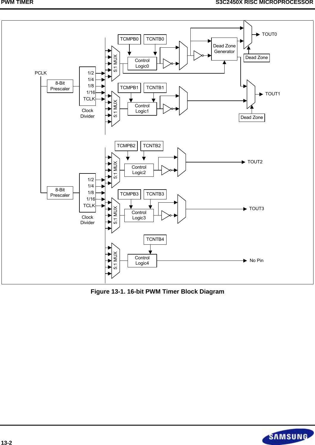
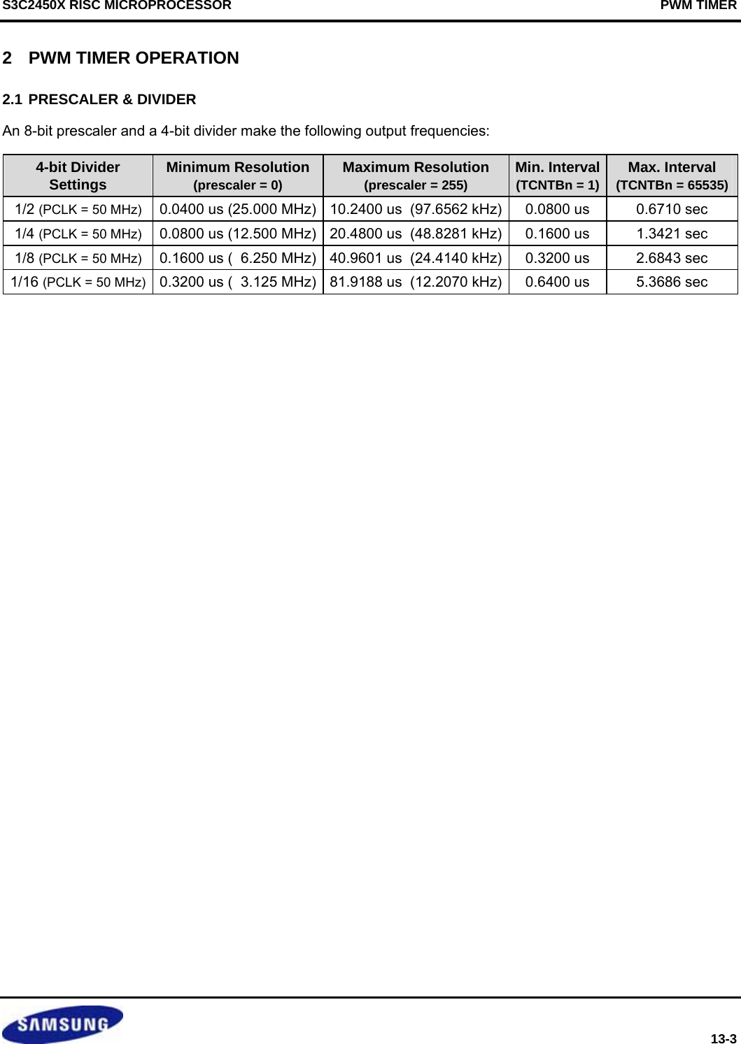
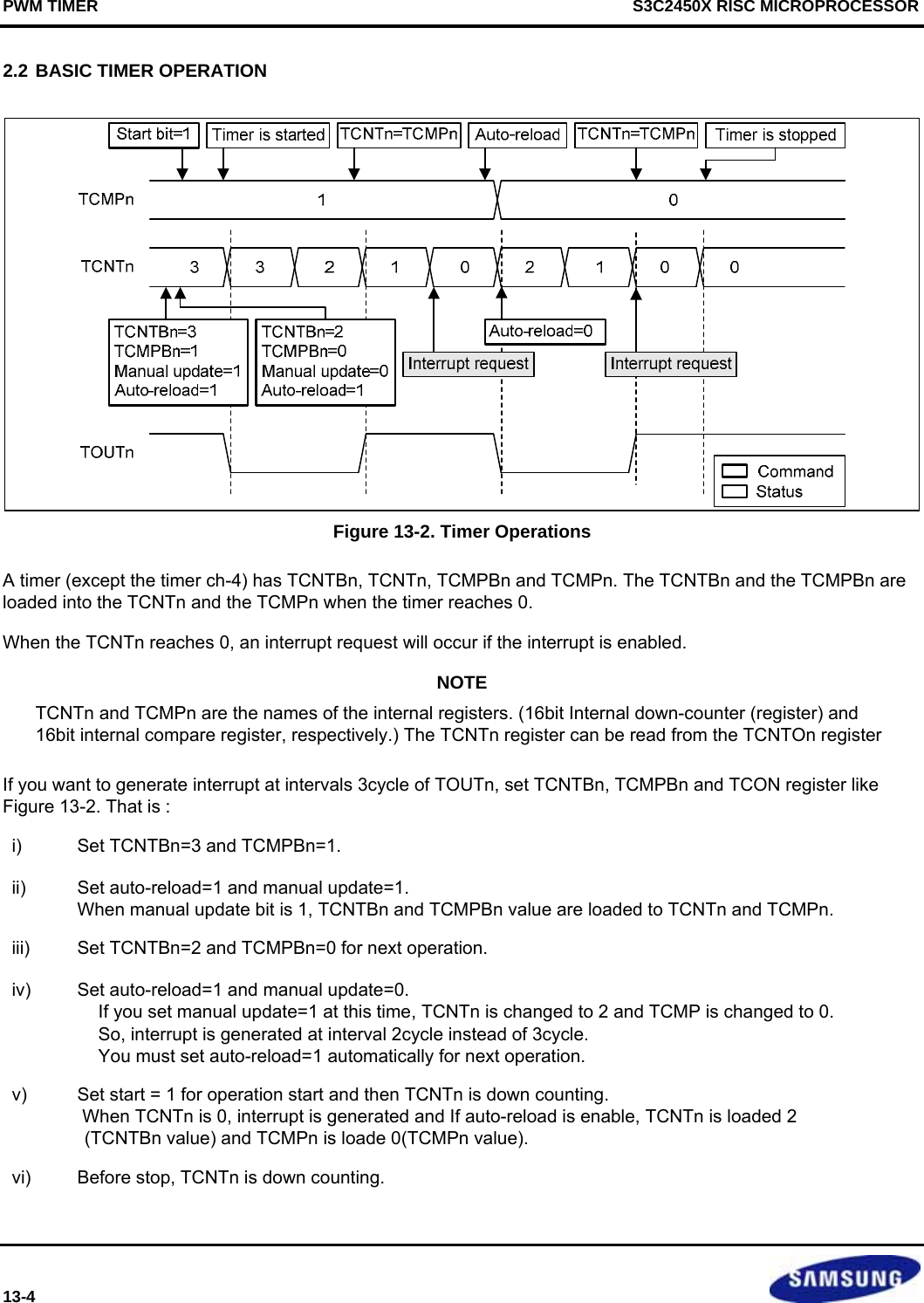
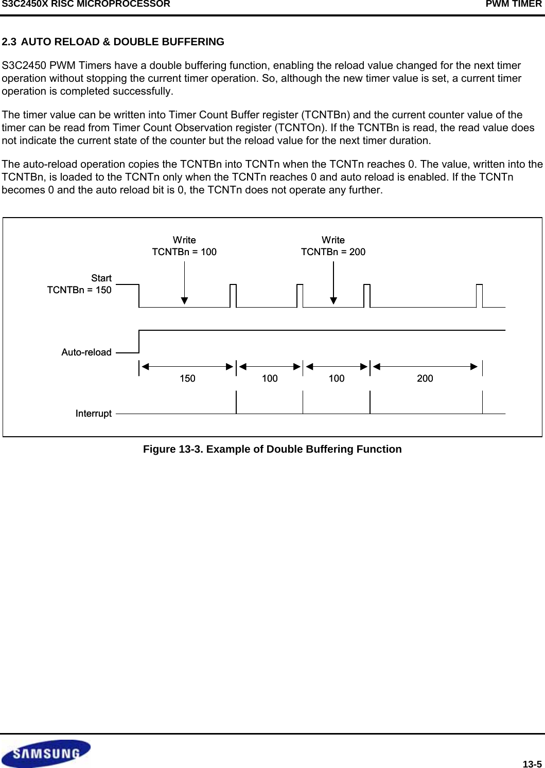
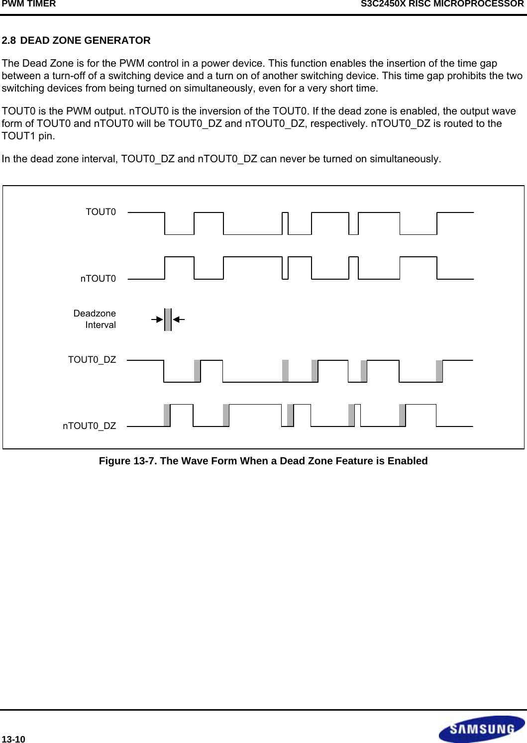
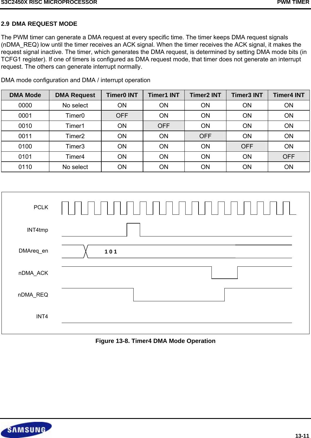
![PWM TIMER S3C2450X RISC MICROPROCESSOR 13-12 3 PWM TIMER CONTROL REGISTERS 3.1 TIMER CONFIGURATION REGISTER0 (TCFG0) Timer input clock Frequency = PCLK / {prescaler value+1} / {divider value} {prescaler value} = 0~255 {divider value} = 2, 4, 8, 16 Register Address R/W Description Reset ValueTCFG0 0x51000000 R/W Configures the two 8-bit prescalers 0x00000000 TCFG0 Bit Description Initial StateReserved [31:24] 0x00 Dead zone length [23:16] These 8 bits determine the dead zone length. The 1 unit time of the dead zone length is equal to that of timer 0. 0x00 Prescaler 1 [15:8] These 8 bits determine prescaler value for Timer 2, 3 and 4. 0x00 Prescaler 0 [7:0] These 8 bits determine prescaler value for Timer 0 and 1. 0x00](https://usermanual.wiki/Diasonic-Technology-Co/RVM-704M.Users-Manual/User-Guide-1826140-Page-348.png)
![S3C2450X RISC MICROPROCESSOR PWM TIMER 13-13 3.2 TIMER CONFIGURATION REGISTER1 (TCFG1) Register Address R/W Description Reset ValueTCFG1 0x51000004 R/W 5-MUX & DMA mode selection register 0x00000000 TCFG1 Bit Description Initial StateReserved [31:24] 00000000 DMA mode [23:20] Select DMA request channel 0000 = No select (all interrupt) 0001 = Timer0 0010 = Timer1 0011 = Timer2 0100 = Timer3 0101 = Timer4 0110 = Reserved 0000 MUX 4 [19:16] Select MUX input for PWM Timer4. 0000 = 1/2 0001 = 1/4 0010 = 1/8 0011 = 1/16 01xx = External TCLK 0000 MUX 3 [15:12] Select MUX input for PWM Timer3. 0000 = 1/2 0001 = 1/4 0010 = 1/8 0011 = 1/16 01xx = External TCLK 0000 MUX 2 [11:8] Select MUX input for PWM Timer2. 0000 = 1/2 0001 = 1/4 0010 = 1/8 0011 = 1/16 01xx = External TCLK 0000 MUX 1 [7:4] Select MUX input for PWM Timer1. 0000 = 1/2 0001 = 1/4 0010 = 1/8 0011 = 1/16 01xx = External TCLK 0000 MUX 0 [3:0] Select MUX input for PWM Timer0. 0000 = 1/2 0001 = 1/4 0010 = 1/8 0011 = 1/16 01xx = External TCLK 0000 Notice) When you use External TCLK, duty of TOUT may show slight error. External TCLK is sampled by PCLK in PWM module. But External TCLK and PCLK is asynchronous clock. So External TCLK may not be sampled at exact time. This slight error can be reduced when External clock is slower than PCLK. So we recommend using External PCLK under 1MHz. (Ex. When PCLK is 66MHz and External PCLK is 1MHz, duty or jitter error can be 1.5%. When PCLK is 66MHz and External PCLK is 0.5MHz, duty or jitter error can be 0.75%)](https://usermanual.wiki/Diasonic-Technology-Co/RVM-704M.Users-Manual/User-Guide-1826140-Page-349.png)
![PWM TIMER S3C2450X RISC MICROPROCESSOR 13-14 3.3 TIMER CONTROL (TCON) REGISTER Register Address R/W Description Reset ValueTCON 0x51000008 R/W Timer control register 0x00000000 TCON Bit Description Initial state Timer 4 auto reload on/off [22] Determine auto reload on/off for Timer 4. 0 = One-shot 1 = Interval mode (auto reload) 0 Timer 4 manual update (note) [21] Determine the manual update for Timer 4. 0 = No operation 1 = Update TCNTB4 0 Timer 4 start/stop [20] Determine start/stop for Timer 4. 0 = Stop 1 = Start for Timer 4 0 Timer 3 auto reload on/off [19] Determine auto reload on/off for Timer 3. 0 = One-shot 1 = Interval mode (auto reload) 0 Timer 3 output inverter on/off [18] Determine output inverter on/off for Timer 3. 0 = Inverter off 1 = Inverter on for TOUT3 0 Timer 3 manual update (note) [17] Determine manual update for Timer 3. 0 = No operation 1 = Update TCNTB3 & TCMPB3 0 Timer 3 start/stop [16] Determine start/stop for Timer 3. 0 = Stop 1 = Start for Timer 3 0 Timer 2 auto reload on/off [15] Determine auto reload on/off for Timer 2. 0 = One-shot 1 = Interval mode (auto reload) 0 Timer 2 output inverter on/off [14] Determine output inverter on/off for Timer 2. 0 = Inverter off 1 = Inverter on for TOUT2 0 Timer 2 manual update (note) [13] Determine the manual update for Timer 2. 0 = No operation 1 = Update TCNTB2 & TCMPB2 0 Timer 2 start/stop [12] Determine start/stop for Timer 2. 0 = Stop 1 = Start for Timer 2 0 Timer 1 auto reload on/off [11] Determine the auto reload on/off for Timer1. 0 = One-shot 1 = Interval mode (auto reload) 0 Timer 1 output inverter on/off [10] Determine the output inverter on/off for Timer1. 0 = Inverter off 1 = Inverter on for TOUT1 0 Timer 1 manual update (note) [9] Determine the manual update for Timer 1. 0 = No operation 1 = Update TCNTB1 & TCMPB1 0 Timer 1 start/stop [8] Determine start/stop for Timer 1. 0 = Stop 1 = Start for Timer 1 0 NOTE: The bits have to be cleared at next writing.](https://usermanual.wiki/Diasonic-Technology-Co/RVM-704M.Users-Manual/User-Guide-1826140-Page-350.png)
![S3C2450X RISC MICROPROCESSOR PWM TIMER 13-15 TCON Bit Description Initial state Reserved [7:5] Reserved Dead zone enable [4] Determine the dead zone operation. 0 = Disable 1 = Enable 0 Timer 0 auto reload on/off [3] Determine auto reload on/off for Timer 0. 0 = One-shot 1 = Interval mode(auto reload) 0 Timer 0 output inverter on/off [2] Determine the output inverter on/off for Timer 0. 0 = Inverter off 1 = Inverter on for TOUT0 0 Timer 0 manual update (note) [1] Determine the manual update for Timer 0. 0 = No operation 1 = Update TCNTB0 & TCMPB0 0 Timer 0 start/stop [0] Determine start/stop for Timer 0. 0 = Stop 1 = Start for Timer 0 0 NOTE: The bit has to be cleared at next writing.](https://usermanual.wiki/Diasonic-Technology-Co/RVM-704M.Users-Manual/User-Guide-1826140-Page-351.png)
![PWM TIMER S3C2450X RISC MICROPROCESSOR 13-16 3.4 TIMER 0 COUNT BUFFER REGISTER & COMPARE BUFFER REGISTER (TCNTB0/TCMPB0) Register Address R/W Description Reset ValueTCNTB0 0x5100000C R/W Timer 0 count buffer register 0x00000000TCMPB0 0x51000010 R/W Timer 0 compare buffer register 0x00000000 TCMPB0 Bit Description Initial StateTimer 0 compare buffer register [15:0] Set compare buffer value for Timer 0 0x00000000 TCNTB0 Bit Description Initial StateTimer 0 count buffer register [15:0] Set count buffer value for Timer 0 0x00000000 3.5 TIMER 0 COUNT OBSERVATION REGISTER (TCNTO0) Register Address R/W Description Reset ValueTCNTO0 0x51000014 R Timer 0 count observation register 0x00000000 TCNTO0 Bit Description Initial StateTimer 0 observation register [15:0] Set count observation value for Timer 0 0x00000000](https://usermanual.wiki/Diasonic-Technology-Co/RVM-704M.Users-Manual/User-Guide-1826140-Page-352.png)
![S3C2450X RISC MICROPROCESSOR PWM TIMER 13-17 3.6 TIMER 1 COUNT BUFFER REGISTER & COMPARE BUFFER REGISTER (TCNTB1/TCMPB1) Register Address R/W Description Reset ValueTCNTB1 0x51000018 R/W Timer 1 count buffer register 0x00000000TCMPB1 0x5100001C R/W Timer 1 compare buffer register 0x00000000 TCMPB1 Bit Description Initial StateTimer 1 compare buffer register [15:0] Set compare buffer value for Timer 1 0x00000000 TCNTB1 Bit Description Initial StateTimer 1 count buffer register [15:0] Set count buffer value for Timer 1 0x00000000 3.7 TIMER 1 COUNT OBSERVATION REGISTER (TCNTO1) Register Address R/W Description Reset ValueTCNTO1 0x51000020 R Timer 1 count observation register 0x00000000 TCNTO1 Bit Description Initial StateTimer 1 observation register [15:0] Set count observation value for Timer 1 0x00000000](https://usermanual.wiki/Diasonic-Technology-Co/RVM-704M.Users-Manual/User-Guide-1826140-Page-353.png)
![PWM TIMER S3C2450X RISC MICROPROCESSOR 13-18 3.8 TIMER 2 COUNT BUFFER REGISTER & COMPARE BUFFER REGISTER (TCNTB2/TCMPB2) Register Address R/W Description Reset ValueTCNTB2 0x51000024 R/W Timer 2 count buffer register 0x00000000TCMPB2 0x51000028 R/W Timer 2 compare buffer register 0x00000000 TCMPB2 Bit Description Initial StateTimer 2 compare buffer register [15:0] Set compare buffer value for Timer 2 0x00000000 TCNTB2 Bit Description Initial StateTimer 2 count buffer register [15:0] Set count buffer value for Timer 2 0x00000000 3.9 TIMER 2 COUNT OBSERVATION REGISTER (TCNTO2) Register Address R/W Description Reset ValueTCNTO2 0x5100002C R Timer 2 count observation register 0x00000000 TCNTO2 Bit Description Initial StateTimer 2 observation register [15:0] Set count observation value for Timer 2 0x00000000](https://usermanual.wiki/Diasonic-Technology-Co/RVM-704M.Users-Manual/User-Guide-1826140-Page-354.png)
![S3C2450X RISC MICROPROCESSOR PWM TIMER 13-19 3.10 TIMER 3 COUNT BUFFER REGISTER & COMPARE BUFFER REGISTER (TCNTB3/TCMPB3) Register Address R/W Description Reset ValueTCNTB3 0x51000030 R/W Timer 3 count buffer register 0x00000000TCMPB3 0x51000034 R/W Timer 3 compare buffer register 0x00000000 TCMPB3 Bit Description Initial StateTimer 3 compare buffer register [15:0] Set compare buffer value for Timer 3 0x00000000 TCNTB3 Bit Description Initial StateTimer 3 count buffer register [15:0] Set count buffer value for Timer 3 0x00000000 3.11 TIMER 3 COUNT OBSERVATION REGISTER (TCNTO3) Register Address R/W Description Reset ValueTCNTO3 0x51000038 R Timer 3 count observation register 0x00000000 TCNTO3 Bit Description Initial StateTimer 3 observation register [15:0] Set count observation value for Timer 3 0x00000000](https://usermanual.wiki/Diasonic-Technology-Co/RVM-704M.Users-Manual/User-Guide-1826140-Page-355.png)
![PWM TIMER S3C2450X RISC MICROPROCESSOR 13-20 3.12 TIMER 4 COUNT BUFFER REGISTER (TCNTB4) Register Address R/W Description Reset ValueTCNTB4 0x5100003C R/W Timer 4 count buffer register 0x00000000 TCNTB4 Bit Description Initial StateTimer 4 count buffer register [15:0] Set count buffer value for Timer 4 0x00000000 3.13 TIMER 4 COUNT OBSERVATION REGISTER (TCNTO4) Register Address R/W Description Reset ValueTCNTO4 0x51000040 R Timer 4 count observation register 0x00000000 TCNTO4 Bit Description Initial StateTimer 4 observation register [15:0] Set count observation value for Timer 4 0x00000000](https://usermanual.wiki/Diasonic-Technology-Co/RVM-704M.Users-Manual/User-Guide-1826140-Page-356.png)
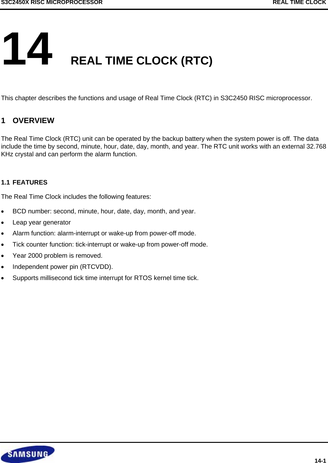
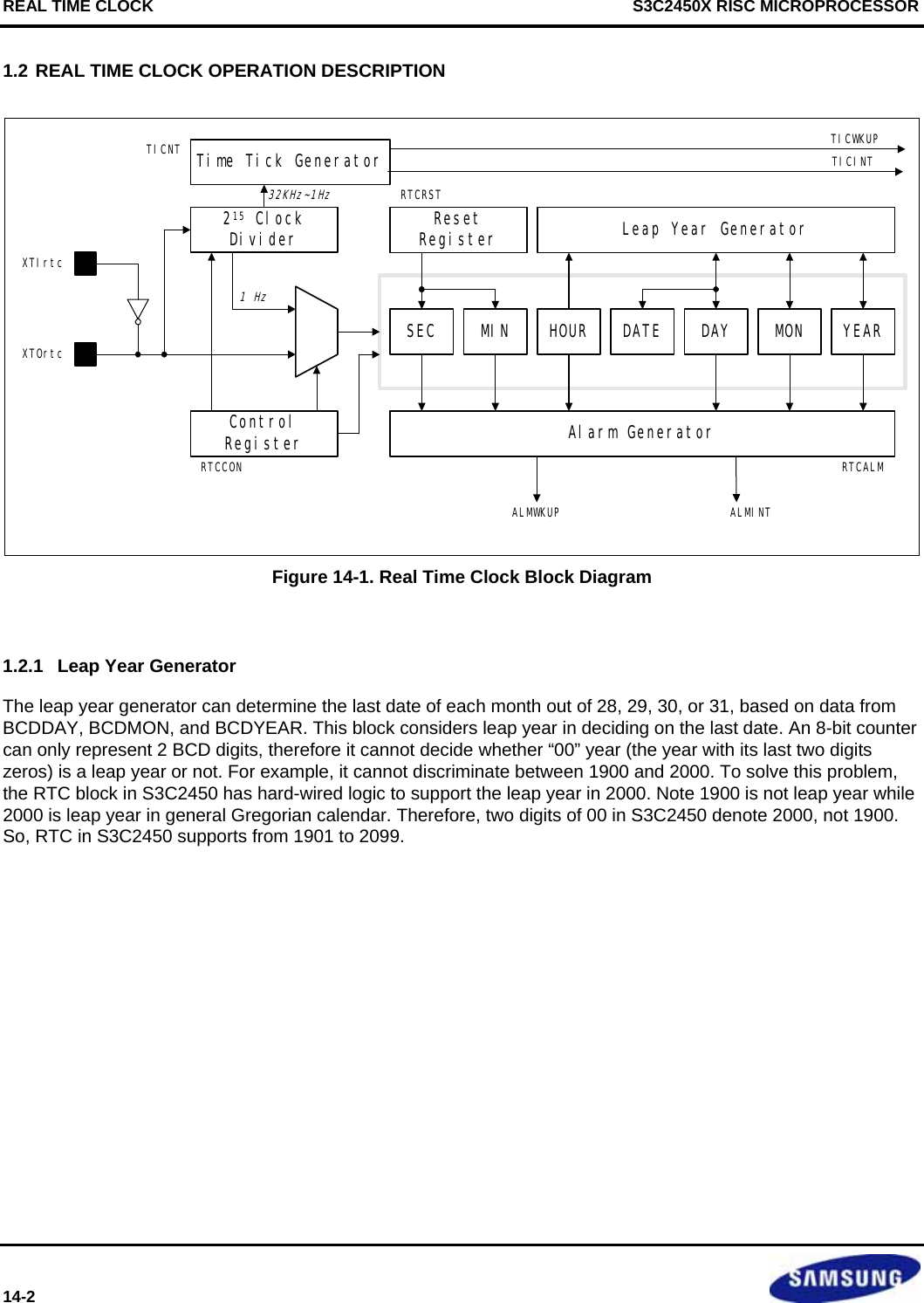
![REAL TIME CLOCK S3C2450X RISC MICROPROCESSOR 14-4 1.2.5 Tick time interrupt The RTC tick time is used for interrupt request. The TICNT register has an interrupt enable bit and the count value for the interrupt. The count value reaches ‘0’ when the tick time interrupt occurs. Then the period of interrupt is as follows: • Tick clock frequency (Hz) = RTC clock / 2n - n: RTC clock divide value(decided by RTCCON[8:4] ) • Resolution = 1 / Tick clock frequency • Clock range = Resolution * 232 Tick counter clock source selection Tick clock source frequency(Hz) Clock range (s) Resolution (ms) TICSel = 1 32768 (2^15) 0 ~ 217 0.03 TICsel2 = 0, TICSel =0 16384 (2^14) 0 ~ 218 0.06 TICsel2 = 1, TICSel =0 8192 (2^13) 0 ~ 219 0.12 TICsel2 = 2, TICSel =0 4096 (2^12) 0 ~220 0.24 TICsel2 = 3, TICSel =0 2048 (2^11) 0 ~ 221 0.49 TICsel2 = 6, TICSel =0 1024 (2^10) 0 ~ 222 0.97 TICsel2 = 7, TICSel =0 512 (2^9) 0 ~ 223 1.95 TICsel2 = 8, TICSel =0 256 (2^8) 0 ~ 224 3.90 TICsel2 = 4, TICSel =0 128 (2^7) 0 ~ 225 7.81 TICsel2 = 9, TICSel =0 64 (2^6) 0 ~ 226 15.62 TICsel2 = 10, TICSel =0 32 (2^5) 0 ~ 227 31.25 TICsel2 = 11, TICSel =0 16 (2^4) 0 ~ 228 62.50 TICsel2 = 12, TICSel =0 8 (2^3) 0 ~ 229 125 TICsel2 = 13, TICSel =0 4 (2^2) 0 ~ 230 250 TICsel2 = 14, TICSel =0 2 0 ~231 500 TICsel2 = 5, TICSel =0 1 0 ~232 1000 NOTE: This RTC time tick may be used for real time operating system (RTOS) kernel time tick. If time tick is generated by the RTC time tick, the time related function of RTOS will always synchronized in real time.](https://usermanual.wiki/Diasonic-Technology-Co/RVM-704M.Users-Manual/User-Guide-1826140-Page-360.png)
![S3C2450X RISC MICROPROCESSOR REAL TIME CLOCK 14-5 Figure 14-2. RTC Tick Interrupt Clock Scheme Example) For 1 ms Tick interrupt generation. 1st ) RTCCON[0]= 1’b1 ( RTC enable ) 2nd) RTCCON[3]=1’b1 ( RTC clock counter reset). 3rd) RTCCON[3] = 1’b0 ( RTC clock counter enable) 4th) RTCCON[8:5] = 4’b0011 ( RTC divide clock selection.) 5th) TICNT1[6:0] = 7’h1 (Tick counter value setting). 6th) TICNT0[7] = 1’b1 (Tick counter enable).](https://usermanual.wiki/Diasonic-Technology-Co/RVM-704M.Users-Manual/User-Guide-1826140-Page-361.png)
![REAL TIME CLOCK S3C2450X RISC MICROPROCESSOR 14-8 1.5 INDIVIDUAL REGISTER DESCRIPTIONS 1.5.1 REAL TIME CLOCK CONTROL (RTCCON) REGISTER The RTCCON register consists of 9 bits. It controls the read/write enable of the CLKSEL, CNTSEL and CLKRST for testing. RTCEN bit can control all interfaces between the CPU and the RTC, Therefore it must be set to 1 in an RTC control routine to enable data read/write after a system reset. Before power off, the RTCEN bit is cleared to 0 to prevent inadvertent writing into BCD counter register. CLKRST is counter reset for 215 Clock divider.(reference to Figure 15-1) Before RTC clock setting, 215 Clock divider must be reset for exact RTC operation. Register Address R/W Description Reset ValueRTCCON 0x57000040 R/W RTC control register 0x00 RTCCON Bit Description Initial State TICsel2 [8:5] Tick Time clock select2. 0 = clock period of 1/16384 second select 1 = clock period of 1/8192 second select 2 = clock period of 1/4096 second select 3 = clock period of 1/2048 second select 4 = clock period of 1/128 second select 5 = clock period of 1 second select 6 = clock period of 1/1024 second select 7 = clock period of 1/512 second select 8 = clock period of 1/256 second select 9 = clock period of 1/64 second select 10 = clock period of 1/32 second select 11 = clock period of 1/16 second select 12 = clock period of 1/8 second select 13 = clock period of 1/4 second select 14 = clock period of 1/2 second select 0x0 TICsel [4] Tick Time clock select1. 0 = Clock period select at TICsel2 1 = Clock period of 1/32768 second 0 CLKRST [3] RTC clock count reset. 0 = No reset 1 = Reset 0 CNTSEL [2] BCD count select. 0 = Merge BCD counters 1 = Reserved (Separate BCD counters) 0 CLKSEL [1] BCD clock select. 0 = XTAL 1/215 divided clock 1 = Reserved (XTAL clock only for test) 0 RTCEN [0] RTC control enable. 0 = Disable 1 = Enable Note: Only BCD time count and read operation can be performed. 0](https://usermanual.wiki/Diasonic-Technology-Co/RVM-704M.Users-Manual/User-Guide-1826140-Page-364.png)
![S3C2450X RISC MICROPROCESSOR REAL TIME CLOCK 14-9 1.5.2 Tick Time Count Register 0 (TICNT0) The TICNT0 register determines tick interrupt enable and tick counter value S3C2450 supports 32bits tic time counter. So, from 14 to 8bits of 32bit tick time count value is selected at TICNT0 register (TICNT0[6:0]). Lower 8bits of 15bit tick time count value is selected at TICNT1 register (TICNT1[7:0]). Upper 17 bits of 32bit tick time count value is selected at TICNT2 register (TICNT0[16:0]). NOTE Tick time count value = (TICK TIME COUNT 0) x 28 + (T ICK TIME COUNT 1) + (TICK TIME COUNT2) x 215 Register Address R/W Description Reset ValueTICNT0 0x57000044 R/W Tick time count register 0x00 TICNT Bit Description Initial StateTICK INT ENABLE [7] Tick time interrupt enable. 0 = Disable 1 = Enable b’0 TICK TIME COUNT 0 [6:0] [14:8] bits of 32 bit tick time count value b’0 1.5.3 Tick Time Count Register 1 (TICNT1) Register Address R/W Description Reset ValueTICNT1 0x5700004C R/W Tick time count register 1 0x00 TICNT1 Bit Description Initial StateTICK TIME COUNT 1 [7:0] Lower 8 bits of 32bit tick time count value b’000000](https://usermanual.wiki/Diasonic-Technology-Co/RVM-704M.Users-Manual/User-Guide-1826140-Page-365.png)
![REAL TIME CLOCK S3C2450X RISC MICROPROCESSOR 14-10 1.5.4 Tick Time Count Register 2 (TICNT2) Register Address R/W Description Reset ValueTICNT2 0x57000048 R/W Tick time count register 2 0x00 TICNT2 Bit Description Initial StateTICK TIME COUNT 2 [16:0] High 17 bits of 32bit tick time count value b’000000 1.5.5 RTC ALARM Control (RTCALM) Register The RTCALM register determines the alarm enable and the alarm time. Note that the RTCALM register generates the alarm signal through both ALMINT and ALMWKUP as power mode. For using ALMINT and ALMWKUP, ALMEN must be enable. If compare value is year, ALMEN and YEAREN must be enable. If compare values are year,mon,date,hour,min and sec, ALMEN,YEAREN,MONEN,DATEEN,HOUREN,MINEN and SECEN must be enable. Register Address R/W Description Reset ValueRTCALM 0x57000050 R/W RTC alarm control register 0x0 RTCALM Bit Description Initial StateReserved [7] 0 ALMEN [6] Alarm global enable 0 = Disable, 1 = Enable Note: For using ALMINT and ALMWKUP, set ALMEN=1’b1 0 YEAREN [5] Year alarm enable 0 = Disable, 1 = Enable 0 MONEN [4] Month alarm enable 0 = Disable, 1 = Enable 0 DATEEN [3] Date alarm enable 0 = Disable, 1 = Enable 0 HOUREN [2] Hour alarm enable 0 = Disable, 1 = Enable 0 MINEN [1] Minute alarm enable 0 = Disable, 1 = Enable 0 SECEN [0] Second alarm enable 0 = Disable, 1 = Enable 0](https://usermanual.wiki/Diasonic-Technology-Co/RVM-704M.Users-Manual/User-Guide-1826140-Page-366.png)
![S3C2450X RISC MICROPROCESSOR REAL TIME CLOCK 14-11 1.5.6 ALARM Second Data (ALMSEC) Register Register Address R/W Description Reset Value ALMSEC 0x57000054 R/W Alarm second data Register 0x0 ALMSEC Bit Description Initial State Reserved [7] 0 [6:4] BCD value for alarm second. 0 ~ 5 000 SECDATA [3:0] 0 ~ 9 0000 1.5.7 ALARM MIN Data (ALMMIN) Register Register Address R/W Description Reset Value ALMMIN 0x57000058 R/W Alarm minute data Register 0x00 ALMMIN Bit Description Initial State Reserved [7] 0 [6:4] BCD value for alarm minute. 0 ~ 5 000 MINDATA [3:0] 0 ~ 9 0000 1.5.8 ALARM HOUR Data (ALMHOUR) Register Register Address R/W Description Reset Value ALMHOUR 0x5700005C R/W Alarm hour data Register 0x0 ALMHOUR Bit Description Initial State Reserved [7:6] 00 [5:4] BCD value for alarm hour. 0 ~ 2 00 HOURDATA [3:0] 0 ~ 9 0000](https://usermanual.wiki/Diasonic-Technology-Co/RVM-704M.Users-Manual/User-Guide-1826140-Page-367.png)
![REAL TIME CLOCK S3C2450X RISC MICROPROCESSOR 14-12 1.5.9 ALARM DATE Data (ALMDATE) Register Register Address R/W Description Reset Value ALMDATE 0x57000060 R/W Alarm day data Register 0x01 ALMDATE Bit Description Initial State Reserved [7:6] 00 [5:4] BCD value for alarm date, from 0 to 28, 29, 30, 31. 0 ~ 3 00 DATEDATA [3:0] 0 ~ 9 0001 1.5.10 ALARM MONTH Data (ALMMON) Register Register Address R/W Description Reset Value ALMMON 0x57000064 R/W Alarm month data Register 0x01 ALMMON Bit Description Initial State Reserved [7:5] 00 [4] BCD value for alarm month. 0 ~ 1 0 MONDATA [3:0] 0 ~ 9 0001 1.5.11 ALARM YEAR Data (ALMYEAR) Register Register Address R/W Description Reset Value ALMYEAR 0x57000068 R/W Alarm year data Register 0x0 ALMYEAR Bit Description Initial State [7:4] BCD value for year. 0~9 0x0 YEARDATA [3:0] 0~9 0x0](https://usermanual.wiki/Diasonic-Technology-Co/RVM-704M.Users-Manual/User-Guide-1826140-Page-368.png)
![S3C2450X RISC MICROPROCESSOR REAL TIME CLOCK 14-13 1.5.12 BCD SECOND (BCDSEC) Register Register Address R/W Description Reset Value BCDSEC 0x57000070 R/W BCD second Register Undefined BCDSEC Bit Description Initial State [6:4] BCD value for second. 0 ~ 5 − SECDATA [3:0] 0 ~ 9 − 1.5.13 BCD MINUTE (BCDMIN) Register Register Address R/W Description Reset Value BCDMIN 0x57000074 R/W BCD minute Register Undefined BCDMIN Bit Description Initial State [6:4] BCD value for minute. 0 ~ 5 − MINDATA [3:0] 0 ~ 9 − 1.5.14 BCD HOUR(BCDHOUR) Register Register Address R/W Description Reset Value BCDHOUR 0x57000078 R/W BCD hour Register Undefined BCDHOUR Bit Description Initial State Reserved [7:6] − [5:4] BCD value for hour. 0 ~ 2 − HOURDATA [3:0] 0 ~ 9 −](https://usermanual.wiki/Diasonic-Technology-Co/RVM-704M.Users-Manual/User-Guide-1826140-Page-369.png)
![REAL TIME CLOCK S3C2450X RISC MICROPROCESSOR 14-14 1.5.15 BCD DATE (BCDDATE) Register Register Address R/W Description Reset Value BCDDATE 0x5700007C R/W BCD DATE Register Undefined BCDDAY Bit Description Initial State Reserved [7:6] − [5:4] BCD value for date. 0 ~ 3 − DATEDATA [3:0] 0 ~ 9 − 1.5.16 BCD DAY (BCDDAY) Register Register Address R/W Description Reset Value BCDDAY 0x57000080 R/W BCD DAY Register Undefined BCDDAY Bit Description Initial State Reserved [7:3] − DAYDATA [2:0] BCD value for a day of the week. 1 ~ 7 − 1.5.17 BCD MONTH (BCDMON) Register Register Address R/W Description Reset Value BCDMON 0x57000084 R/W BCD month Register Undefined BCDMON Bit Description Initial State Reserved [7:5] − [4] BCD value for month. 0 ~ 1 − MONDATA [3:0] 0 ~ 9 −](https://usermanual.wiki/Diasonic-Technology-Co/RVM-704M.Users-Manual/User-Guide-1826140-Page-370.png)
![S3C2450X RISC MICROPROCESSOR REAL TIME CLOCK 14-15 1.5.18 BCD YEAR (BCDYEAR) Register Register Address R/W Description Reset Value BCDYEAR 0x57000088 R/W BCD year Register Undefined BCDYEAR Bit Description Initial State [7:4] BCD value for year. 0~9 0x0 YEARDATA [3:0] 0~9 0x0 NOTE: For setting BCD registers, RTCEN(RTCCON[0] bit) must be ebable. But at no setting BCD registers, RTCEN must be disable for reducing power comsumption. 1.5.19 TICK Counter Register Register Address R/W Description Reset Value TICKCNT 0x57000090 R Internal tick time counter register 0x00 TICKCNT Bit Description Initial State TICKCNT [31:0] Internal tick counter. Only readable 0 ~ 4294967295 0](https://usermanual.wiki/Diasonic-Technology-Co/RVM-704M.Users-Manual/User-Guide-1826140-Page-371.png)

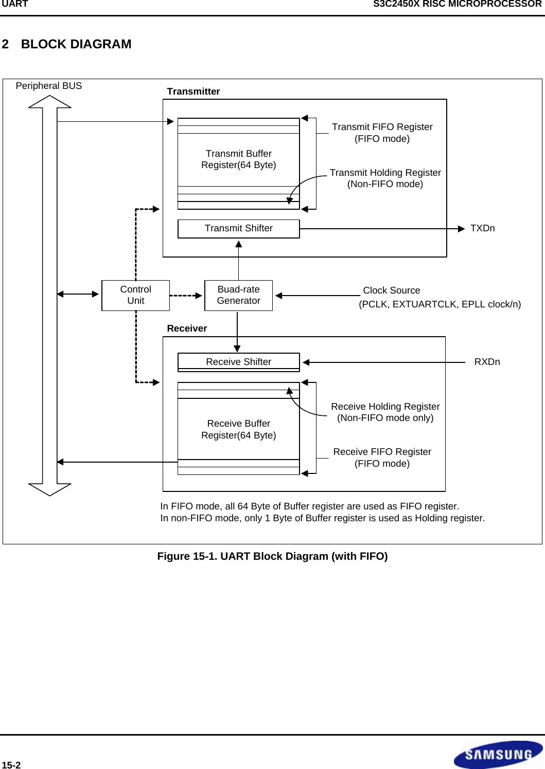
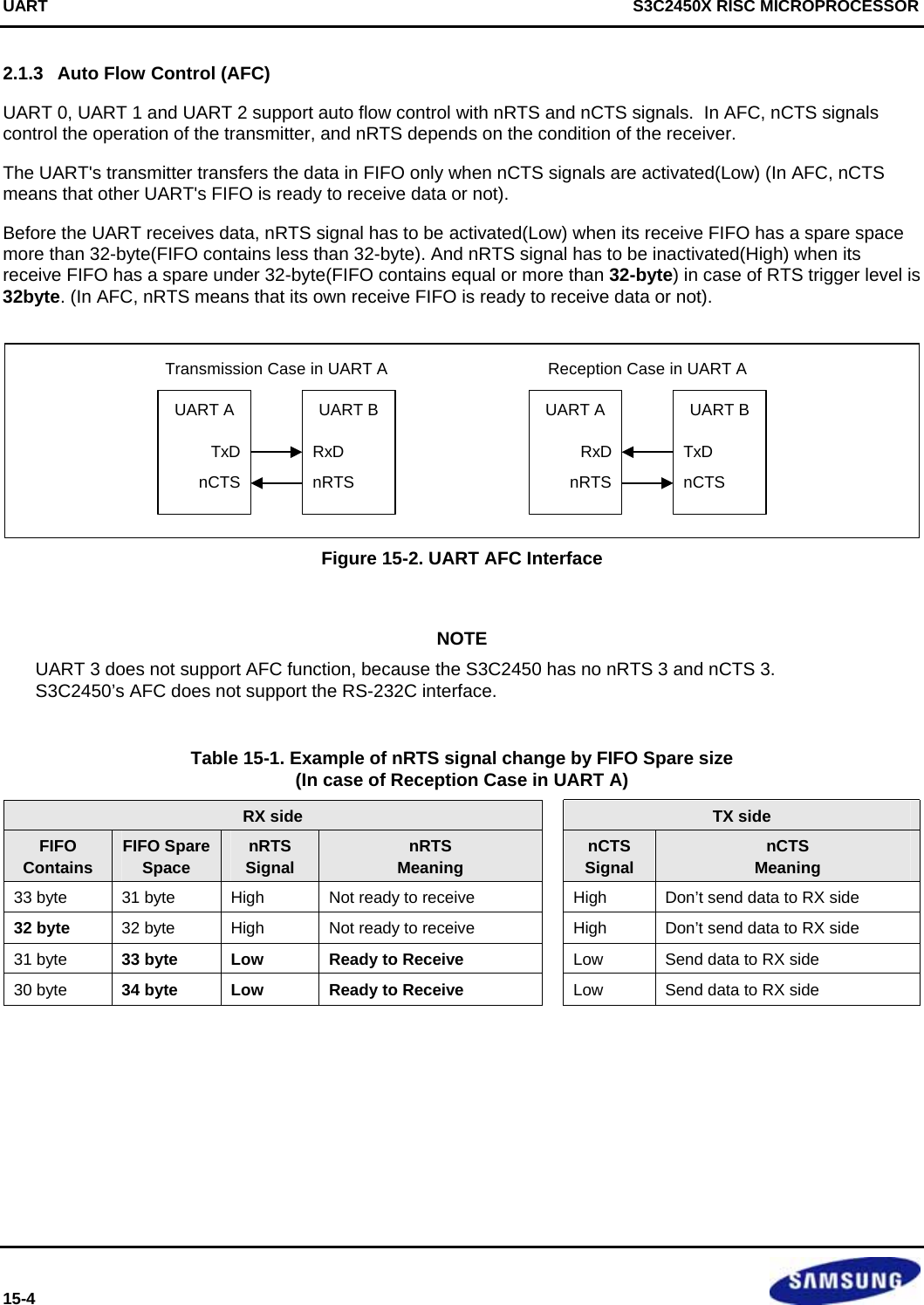
![S3C2450X RISC MICROPROCESSOR UART 15-5 2.1.4 Non Auto-Flow Control (Controlling nRTS and nCTS by Software) If users want to connect a UART to a Modem, disable auto flow control bit in UMCONn register and control the signal of nRTS by software. Example: Rx Operation with FIFO 1. Select receive mode (Interrupt or DMA mode). 2. Check the value of Rx FIFO count in UFSTATn register. If the value is less than 32, users have to set the value of UMCONn[0] to '1' (activating nRTS), and if it is equal or larger than 32 users have to set the value to '0' (inactivating nRTS). 3. Repeat the Step 2. Tx Operation with FIFO 1. Select transmit mode (Interrupt or DMA mode). 2. Check the value of UMSTATn[0]. If the value is '1' (activating nCTS), users write the data to Tx FIFO register. 3. Repeat the Step 2. 2.1.5 RS-232C Interface If the user wants to connect the UART to modem interface (instead of null modem), nRTS, nCTS, nDSR, nDTR, DCD and nRI signals are needed. In this case, the users can control these signals with general I/O ports by software because the AFC does not support the RS-232C interface.](https://usermanual.wiki/Diasonic-Technology-Co/RVM-704M.Users-Manual/User-Guide-1826140-Page-377.png)
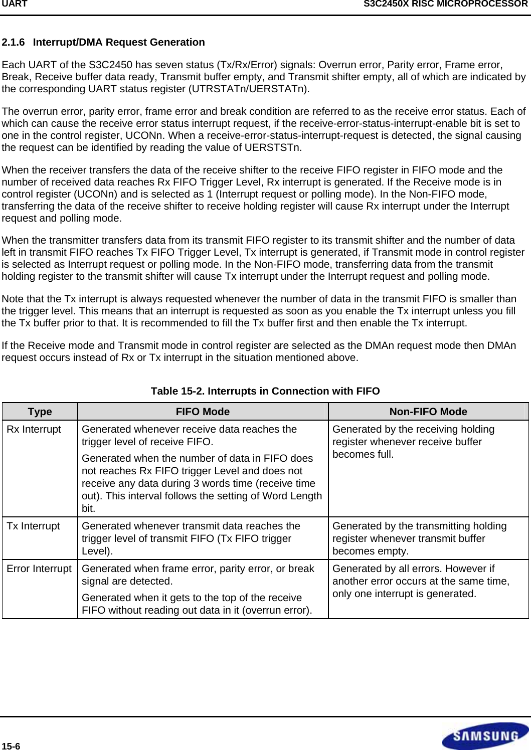
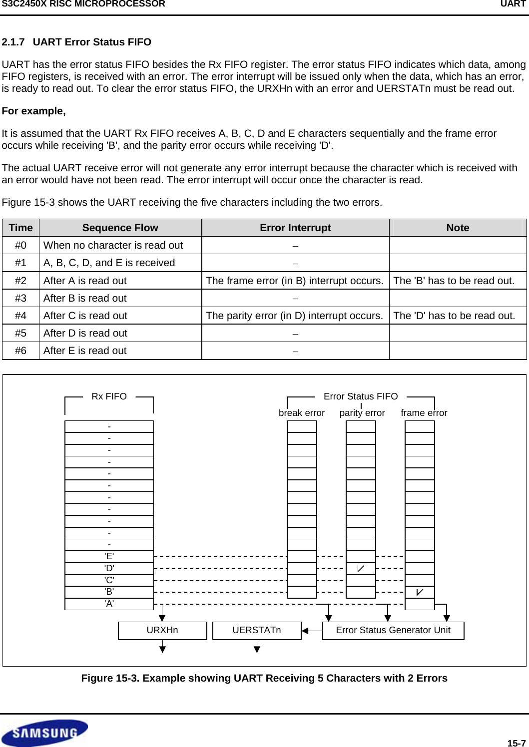
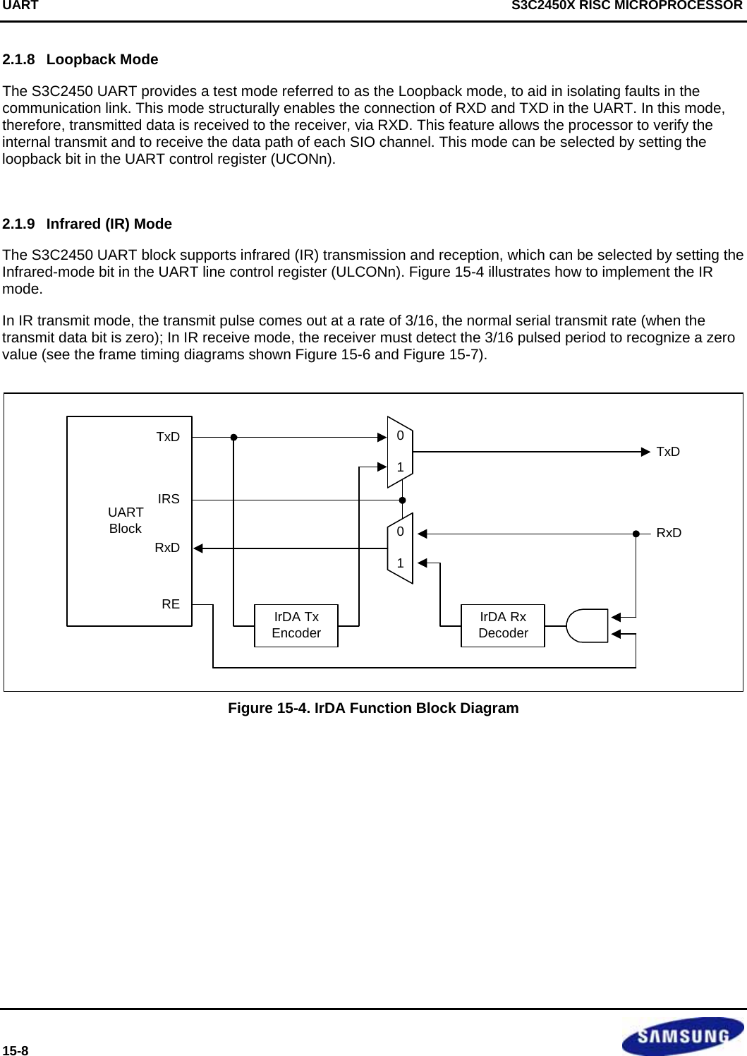
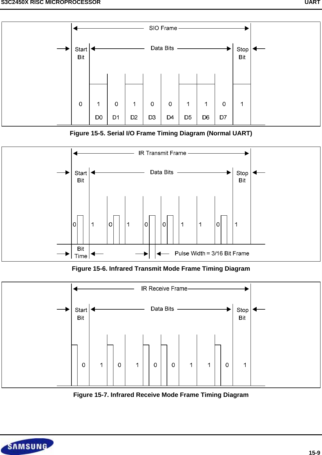
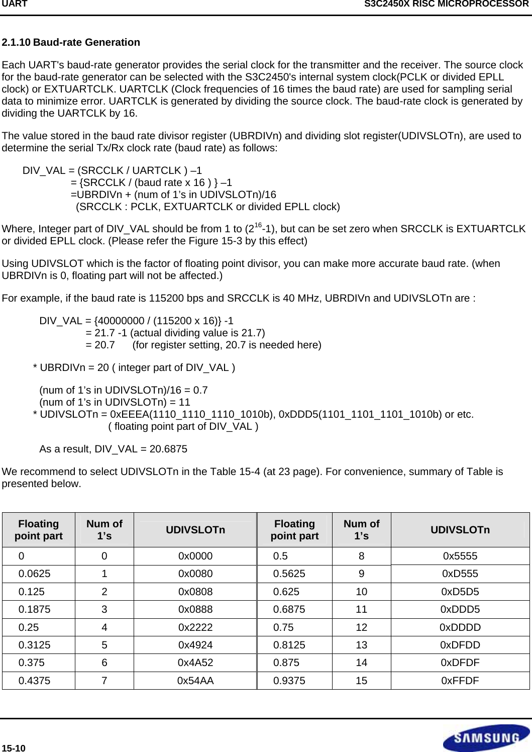
![UART S3C2450X RISC MICROPROCESSOR 15-12 3 UART SPECIAL REGISTERS 3.1 UART LINE CONTROL REGISTER There are four UART line control registers including ULCON0, ULCON1, ULCON2 and ULCON3 in the UART block. Register Address R/W Description Reset ValueULCON0 0x50000000 R/W UART channel 0 line control register 0x00 ULCON1 0x50004000 R/W UART channel 1 line control register 0x00 ULCON2 0x50008000 R/W UART channel 2 line control register 0x00 ULCON3 0x5000C000 R/W UART channel 3 line control register 0x00 ULCONn Bit Description Initial StateReserved [7] − 0 Infrared Mode [6] Determine whether or not to use the Infrared mode. 0 = Normal mode operation 1 = Infrared Tx/Rx mode 0 Parity Mode [5:3] Specify the type of parity generation and checking during UART transmit and receive operation. 0xx = No parity 100 = Odd parity 101 = Even parity 110 = Parity forced/checked as 1 111 = Parity forced/checked as 0 000 Number of Stop Bit [2] Specify how many stop bits are to be used for end-of-frame signal. 0 = One stop bit per frame 1 = Two stop bit per frame 0 Word Length [1:0] Indicate the number of data bits to be transmitted or received per frame. 00 = 5-bits 01 = 6-bits 10 = 7-bits 11 = 8-bits 00](https://usermanual.wiki/Diasonic-Technology-Co/RVM-704M.Users-Manual/User-Guide-1826140-Page-384.png)
![S3C2450X RISC MICROPROCESSOR UART 15-13 3.2 UART CONTROL REGISTER There are four UART control registers including UCON0, UCON1, UCON2 and UCON3 in the UART block. Register Address R/W Description Reset ValueUCON0 0x50000004 R/W UART channel 0 control register 0x00 UCON1 0x50004004 R/W UART channel 1 control register 0x00 UCON2 0x50008004 R/W UART channel 2 control register 0x00 UCON3 0x5000C004 R/W UART channel 3 control register 0x00 UCONn Bit Description Initial StateClock Selection [11:10] Select PCLK, EXTUARTCLK(External UART clock) or divided EPLL clock for source clock of the UART. (note 5) 00, 10 (note 1) = PCLK 01 = EXTUARTCLK 11 = Divided EPLL clock (Refer to the Clock divider control register1 (CLKDIV1) in the system controller). 0 Tx Interrupt Type [9] Interrupt request type. 0 = Pulse (Interrupt is requested as soon as the Tx buffer becomes empty in Non-FIFO mode or reaches Tx FIFO Trigger Level in FIFO mode.) 0 Rx Interrupt Type [8] Interrupt request type. 0 = Pulse (Interrupt is requested the instant Rx buffer receives the data in Non-FIFO mode or reaches Rx FIFO Trigger Level in FIFO mode.) 0 Rx Time Out Enable [7] Enable/Disable Rx time out interrupt when UART FIFO is enabled. The interrupt is a receive interrupt. (note 2) 0 = Disable 1 = Enable 0 Rx Error Status Interrupt Enable [6] Enable the UART to generate an interrupt upon an exception, such as a break, frame error, parity error, or overrun error during a receive operation. 0 = Do not generate receive error status interrupt. 1 = Generate receive error status interrupt. 0 Loopback Mode [5] Setting loopback bit to 1 causes the UART to enter the loopback mode. This mode is provided for test purposes only. 0 = Normal operation 1 = Loopback mode 0 Send break signal [4] Setting this bit causes the UART to send a break during 1 frame time. This bit is auto-cleared after sending the break signal 0 = Normal transmit 1 = Send break signal 0](https://usermanual.wiki/Diasonic-Technology-Co/RVM-704M.Users-Manual/User-Guide-1826140-Page-385.png)
![UART S3C2450X RISC MICROPROCESSOR 15-14 UCONn Bit Description Initial StateTransmit Mode (note 3) [3:2] Determine which function is currently able to write Tx data to the UART transmit buffer register. 00 = Disable 01 = Interrupt request (note 6) or polling mode 10 = DMA request( request signal 0) 11 = DMA request( request signal 1) 00 Receive Mode [1:0] Determine which function is currently able to read data from UART receive buffer register. 00 = Disable (note 4) 01 = Interrupt request or polling mode 10 = DMA request( request signal 0) 11 = DMA request( request signal 1) 00 NOTES: 1. When you want to change EXTUARTCLK to PCLK for UART baudrate, clock selection field must be set to 2’b10. 2. When the UART does not reach the FIFO trigger level and does not receive data during 3 words time in Interrupt receive mode with FIFO, the Rx interrupt will be generated (receive time out), and the users should check the FIFO status and read out the rest. 3. If Tx DMA request signal were 0, Rx DMA request signal should be 1. They can’t share request signal 0 or 1 in common. (UCONn[3:2], UCONn[1:0]) = (“10b”, “11b”) or (“11b”, “10b”) 4. When Receive mode is enabled, changing of GPIO status affect to RXD line(example : GPIO RXD ->GPIO input -> GPIO RXD), dummy data can be read at RX FIFO. Recommended steps are follows. - Disable Receive Mode - Set GPIO as UART mode. - RX FIFO reset. - Interrupt unmask(enable) if needed - Enable Receive Mode(Set Receive Mode to Interrupt/DMA request or polling mode) 5. In the middle of operation, changing source clock selection or speed of source clock is prohibited. These must be done after finishing transmission/receiving 6. Mask bit of INTMSK(Interrupt Mask Register ) should be 0 (unmask) before enabling Transmit mode as Interrupt request mode.](https://usermanual.wiki/Diasonic-Technology-Co/RVM-704M.Users-Manual/User-Guide-1826140-Page-386.png)
![S3C2450X RISC MICROPROCESSOR UART 15-15 3.3 UART FIFO CONTROL REGISTER There are four UART FIFO control registers including UFCON0, UFCON1, UFCON2 and UFCON3 in the UART block. Register Address R/W Description Reset ValueUFCON0 0x50000008 R/W UART channel 0 FIFO control register 0x0 UFCON1 0x50004008 R/W UART channel 1 FIFO control register 0x0 UFCON2 0x50008008 R/W UART channel 2 FIFO control register 0x0 UFCON3 0x5000C008 R/W UART channel 3 FIFO control register 0x0 UFCONn Bit Description Initial StateTx FIFO Trigger Level (note 2) [7:6] Determine the trigger level of transmit FIFO. 00 = Empty 01 = 16-byte 10 = 32-byte 11 = 48-byte 00 Rx FIFO Trigger Level (note 2) [5:4] Determine the trigger level of receive FIFO. 00 = 1-byte 01 = 8-byte 10 = 16-byte 11 = 32-byte 00 Reserved [3] − 0 Tx FIFO Reset [2] Auto-cleared after resetting FIFO 0 = Normal 1 = Tx FIFO reset 0 Rx FIFO Reset [1] Auto-cleared after resetting FIFO 0 = Normal 1 = Rx FIFO reset 0 FIFO Enable (note 2) [0] 0 = Disable (note 1) 1 = Enable 0 NOTES: 1. At DMA mode, FIFO Enable should be Disabled. 2. Please refer the following recommendation for Interrupt / DMA mode. Mode FIFO enable TX FIFO Trigger level RX FIFO Trigger level RX time out enable Interrupt mode Enable (FIFO mode) 16~48byte 8~32byte enable DMA mode Disable (Non-FIFO mode) n/a n/a n/a](https://usermanual.wiki/Diasonic-Technology-Co/RVM-704M.Users-Manual/User-Guide-1826140-Page-387.png)
![UART S3C2450X RISC MICROPROCESSOR 15-16 3.4 UART MODEM CONTROL REGISTER There are three UART MODEM control registers including UMCON0 and UMCON1 in the UART block. Register Address R/W Description Reset ValueUMCON0 0x5000000C R/W UART channel 0 Modem control register 0x0 UMCON1 0x5000400C R/W UART channel 1 Modem control register 0x0 UMCON2 0x5000800C R/W UART channel 2 Modem control register 0x0 UMCONn Bit Description Initial StateRTS trigger Level [7:5] When AFC bit is enabled, these bits determine when to inactivate (High) nRTS signal. 000 = When RX FIFO contains 63 bytes. 001 = When RX FIFO contains 56 bytes. 010 = When RX FIFO contains 48 bytes. 011 = When RX FIFO contains 40 bytes. 100 = When RX FIFO contains 32 bytes. 101 = When RX FIFO contains 24 bytes. 110 = When RX FIFO contains 16 bytes. 111 = When RX FIFO contains 8 bytes. 000 Auto Flow Control (AFC) [4] 0 = Disable 1 = Enable 0 Reserved [3:1] These bits must be 0's 00 Request to Send [0] If AFC bit is enabled, this value will be ignored. In this case the S3C2450 will control nRTS automatically. If AFC bit is disabled, nRTS must be controlled by software. 0 = 'H' level (Inactivate nRTS) 1 = 'L' level (Activate nRTS) 0 NOTES: 1. UART 3 does not support AFC function, because the S3C2450 has no nRTS3 and nCTS3. 2. If AFC bit is enabled and Time-out bit is disabled, RTS trigger level must be lager than Rx FIFO trigger level. 3. Example ) RX interrupt mode, RTS trigger level b101(24byte), RX FIFO trigger level b10(16byte). This example shows RX FIFO always contains equal or less than 24 bytes. (have space equal or larger than 40bytes.) FIFO contains FIFO Spare space nRTS signal Interrupt Note 24 byte 40 byte High - RTS trigger Level 23 byte 41 byte Low - … … Low - 17 byte 47 byte Low - 16 byte 48 byte Low Occur RX FIFO trigger Level 15 byte 49 byte Low -](https://usermanual.wiki/Diasonic-Technology-Co/RVM-704M.Users-Manual/User-Guide-1826140-Page-388.png)
![S3C2450X RISC MICROPROCESSOR UART 15-17 3.5 UART TX/RX STATUS REGISTER There are four UART Tx/Rx status registers including UTRSTAT0, UTRSTAT1, UTRSTAT2 and UTRSTAT3 in the UART block. Register Address R/W Description Reset ValueUTRSTAT0 0x50000010 R UART channel 0 Tx/Rx status register 0x6 UTRSTAT1 0x50004010 R UART channel 1 Tx/Rx status register 0x6 UTRSTAT2 0x50008010 R UART channel 2 Tx/Rx status register 0x6 UTRSTAT3 0x5000C010 R UART channel 3 Tx/Rx status register 0x6 UTRSTATn Bit Description Initial StateTransmitter empty [2] Set to 1 automatically when the transmit buffer register has no valid data to transmit and the transmit shift register is empty. 0 = Not empty 1 = Transmitter (transmit buffer & shifter register) empty 1 Transmit buffer empty [1] Set to 1 automatically when transmit buffer register is empty. 0 =The buffer register is not empty 1 = Empty (In Non-FIFO mode, Interrupt or DMA is requested. In FIFO mode, Interrupt or DMA is requested, when Tx FIFO Trigger Level is set to 00 (Empty)) If the UART uses the FIFO, users should check Tx FIFO Count bits and Tx FIFO Full bit in the UFSTAT register instead of this bit. 1 Receive buffer data ready [0] Set to 1 automatically whenever receive buffer register contains valid data, received over the RXDn port. 0 = Empty 1 = The buffer register has a received data (In Non-FIFO mode, Interrupt or DMA is requested) If the UART uses the FIFO, users should check Rx FIFO Count bits and Rx FIFO Full bit in the UFSTAT register instead of this bit. 0](https://usermanual.wiki/Diasonic-Technology-Co/RVM-704M.Users-Manual/User-Guide-1826140-Page-389.png)
![UART S3C2450X RISC MICROPROCESSOR 15-18 3.6 UART ERROR STATUS REGISTER There are four UART Rx error status registers including UERSTAT0, UERSTAT1, UERSTAT2 and UERSTAT3 in the UART block. Register Address R/W Description Reset ValueUERSTAT0 0x50000014 R UART channel 0 Rx error status register 0x0 UERSTAT1 0x50004014 R UART channel 1 Rx error status register 0x0 UERSTAT2 0x50008014 R UART channel 2 Rx error status register 0x0 UERSTAT3 0x5000C014 R UART channel 3 Rx error status register 0x0 UERSTATn Bit Description Initial StateBreak Detect [3] Set to 1 automatically to indicate that a break signal has been received. 0 = No break receive 1 = Break receive (Interrupt is requested.) 0 Frame Error [2] Set to 1 automatically whenever a frame error occurs during receive operation. 0 = No frame error during receive 1 = Frame error (Interrupt is requested.) 0 Parity Error [1] Set to 1 automatically whenever a parity error occurs during receive operation. 0 = No parity error during receive 1 = Parity error (Interrupt is requested.) 0 Overrun Error [0] Set to 1 automatically whenever an overrun error occurs during receive operation. 0 = No overrun error during receive 1 = Overrun error (Interrupt is requested.) 0 NOTE: These bits (UERSATn[3:0]) are automatically cleared to 0 when the UART error status register is read.](https://usermanual.wiki/Diasonic-Technology-Co/RVM-704M.Users-Manual/User-Guide-1826140-Page-390.png)
![S3C2450X RISC MICROPROCESSOR UART 15-19 3.7 UART FIFO STATUS REGISTER There are four UART FIFO status registers including UFSTAT0, UFSTAT1 UFSTAT2 and UFSTAT3 in the UART block. Register Address R/W Description Reset ValueUFSTAT0 0x50000018 R UART channel 0 FIFO status register 0x00 UFSTAT1 0x50004018 R UART channel 1 FIFO status register 0x00 UFSTAT2 0x50008018 R UART channel 2 FIFO status register 0x00 UFSTAT3 0x5000C018 R UART channel 3 FIFO status register 0x00 UFSTATn Bit Description Initial StateReserved [15] − 0 Tx FIFO Full [14] Set to 1 automatically whenever transmit FIFO is full during transmit operation 0 = 0-byte ≤ Tx FIFO data ≤ 63-byte 1 = Full 0 Tx FIFO Count [13:8] Number of data in Tx FIFO 0 Reserved [7] − 0 Rx FIFO Full [6] Set to 1 automatically whenever receive FIFO is full during receive operation 0 = 0-byte ≤ Rx FIFO data ≤ 63-byte 1 = Full 0 Rx FIFO Count [5:0] Number of data in Rx FIFO 0](https://usermanual.wiki/Diasonic-Technology-Co/RVM-704M.Users-Manual/User-Guide-1826140-Page-391.png)
![UART S3C2450X RISC MICROPROCESSOR 15-20 3.8 UART MODEM STATUS REGISTER There are three UART modem status registers including UMSTAT0, UMSTAT1 in the UART block. Register Address R/W Description Reset ValueUMSTAT0 0x5000001C R UART channel 0 modem status register 0x0 UMSTAT1 0x5000401C R UART channel 1 modem status register 0x0 UMSTAT2 0x5000801C R UART channel 2 modem status register 0x0 UMSTAT0 Bit Description Initial StateDelta CTS [4] Indicate that the nCTS input to the S3C2450 has changed state since the last time it was read by CPU. (Refer to Figure 15-8.) 0 = Has not changed 1 = Has changed 0 Reserved [3:1] − 0 Clear to Send [0] 0 = CTS signal is not activated (nCTS pin is high) 1 = CTS signal is activated (nCTS pin is low) 0 nCTSDelta CTSRead_UMSTAT Figure 15-8. nCTS and Delta CTS Timing Diagram](https://usermanual.wiki/Diasonic-Technology-Co/RVM-704M.Users-Manual/User-Guide-1826140-Page-392.png)
![S3C2450X RISC MICROPROCESSOR UART 15-21 3.9 UART TRANSMIT BUFFER REGISTER (HOLDING REGISTER & FIFO REGISTER) There are four UART transmit buffer registers including UTXH0, UTXH1, UTXH2 and UTXH3 in the UART block. UTXHn has an 8-bit data for transmission data. Register Address R/W Description Reset ValueUTXH0 0x50000020 W (by byte) UART channel 0 transmit buffer register − UTXH1 0x50004020 W (by byte) UART channel 1 transmit buffer register − UTXH2 0x50008020 W (by byte) UART channel 2 transmit buffer register − UTXH3 0x5000C020 W (by byte) UART channel 3 transmit buffer register − UTXHn Bit Description Initial StateTXDATAn [7:0] Transmit data for UARTn − 3.10 UART RECEIVE BUFFER REGISTER (HOLDING REGISTER & FIFO REGISTER) There are four UART receive buffer registers including URXH0, URXH1, URXH2 and URXH3 in the UART block. URXHn has an 8-bit data for received data. Register Address R/W Description Reset ValueURXH0 0x50000024 R (by byte) UART channel 0 receive buffer register − URXH1 0x50004024 R (by byte) UART channel 1 receive buffer register − URXH2 0x50008024 R (by byte) UART channel 2 receive buffer register − URXH3 0x5000C024 R (by byte) UART channel 3 receive buffer register − URXHn Bit Description Initial StateRXDATAn [7:0] Receive data for UARTn – NOTE: When an overrun error occurs, the URXHn must be read. If not, the next received data will also make an overrun error, even though the overrun bit of UERSTATn had been cleared.](https://usermanual.wiki/Diasonic-Technology-Co/RVM-704M.Users-Manual/User-Guide-1826140-Page-393.png)
![UART S3C2450X RISC MICROPROCESSOR 15-22 3.11 UART BAUD RATE DIVISOR REGISTER There are four UART baud rate divisor registers including UBRDIV0, UBRDIV1, UBRDIV2 and UBRDIV3 in the UART block. Register Address R/W Description Reset ValueUBRDIV0 0x50000028 R/W Baud rate divisior(integer place) register 0 − UBRDIV1 0x50004028 R/W Baud rate divisior(integer place) register 1 − UBRDIV2 0x50008028 R/W Baud rate divisior(integer place) register 2 − UBRDIV3 0x5000C028 R/W Baud rate divisior(integer place) register 3 − UBRDIVn Bit Description Initial StateUBRDIV [15:0] Baud rate division value of integer part (When UART clock source is PCLK, UBRDIVn must be more than 0 (UBRDIVn >0)) − NOTE: If UBRDIV value is 0, UART baudrate is not affected by UDIVSLOT value.](https://usermanual.wiki/Diasonic-Technology-Co/RVM-704M.Users-Manual/User-Guide-1826140-Page-394.png)
![S3C2450X RISC MICROPROCESSOR UART 15-23 3.12 UART DIVIDING SLOT REGISTER There are four UART dividing slot registers including UDIVSLOT0, UDIVSLOT 1, UDIVSLOT 2 and UDIVSLOT in the UART block. Register Address R/W Description Reset ValueUDIVSLOT0 0x5000002C R/W Baud rate divisior(decimal place) register 0 0x0000 UDIVSLOT1 0x5000402C R/W Baud rate divisior(decimal place) register 1 0x0000 UDIVSLOT2 0x5000802C R/W Baud rate divisior(decimal place) register 2 0x0000 UDIVSLOT3 0x5000C02C R/W Baud rate divisior(decimal place) register 3 0x0000 UDIVSLOTn Bit Description Initial StateUDIVSLOT [15:0] Select the slot number in Table 15-4 − Table 15-4. Recommended Value Table of DIVSLOTn Register Floating point part Num of 1’s UDIVSLOTn 0 0 0x0000(0000_0000_0000_0000b) 0.0625 1 0x0080(0000_0000_0000_1000b) 0.125 2 0x0808(0000_1000_0000_1000b) 0.1875 3 0x0888(0000_1000_1000_1000b) 0.25 4 0x2222(0010_0010_0010_0010b) 0.3125 5 0x4924(0100_1001_0010_0100b) 0.375 6 0x4A52(0100_1010_0101_0010b) 0.4375 7 0x54AA(0101_0100_1010_1010b) 0.5 8 0x5555(0101_0101_0101_0101b) 0.5625 9 0xD555(1101_0101_0101_0101b) 0.625 10 0xD5D5(1101_0101_1101_0101b) 0.6875 11 0xDDD5(1101_1101_1101_0101b) 0.75 12 0xDDDD(1101_1101_1101_1101b) 0.8125 13 0xDFDD(1101_1111_1101_1101b) 0.875 14 0xDFDF(1101_1111_1101_1111b) 0.9375 15 0xFFDF(1111_1111_1101_1111b)](https://usermanual.wiki/Diasonic-Technology-Co/RVM-704M.Users-Manual/User-Guide-1826140-Page-395.png)

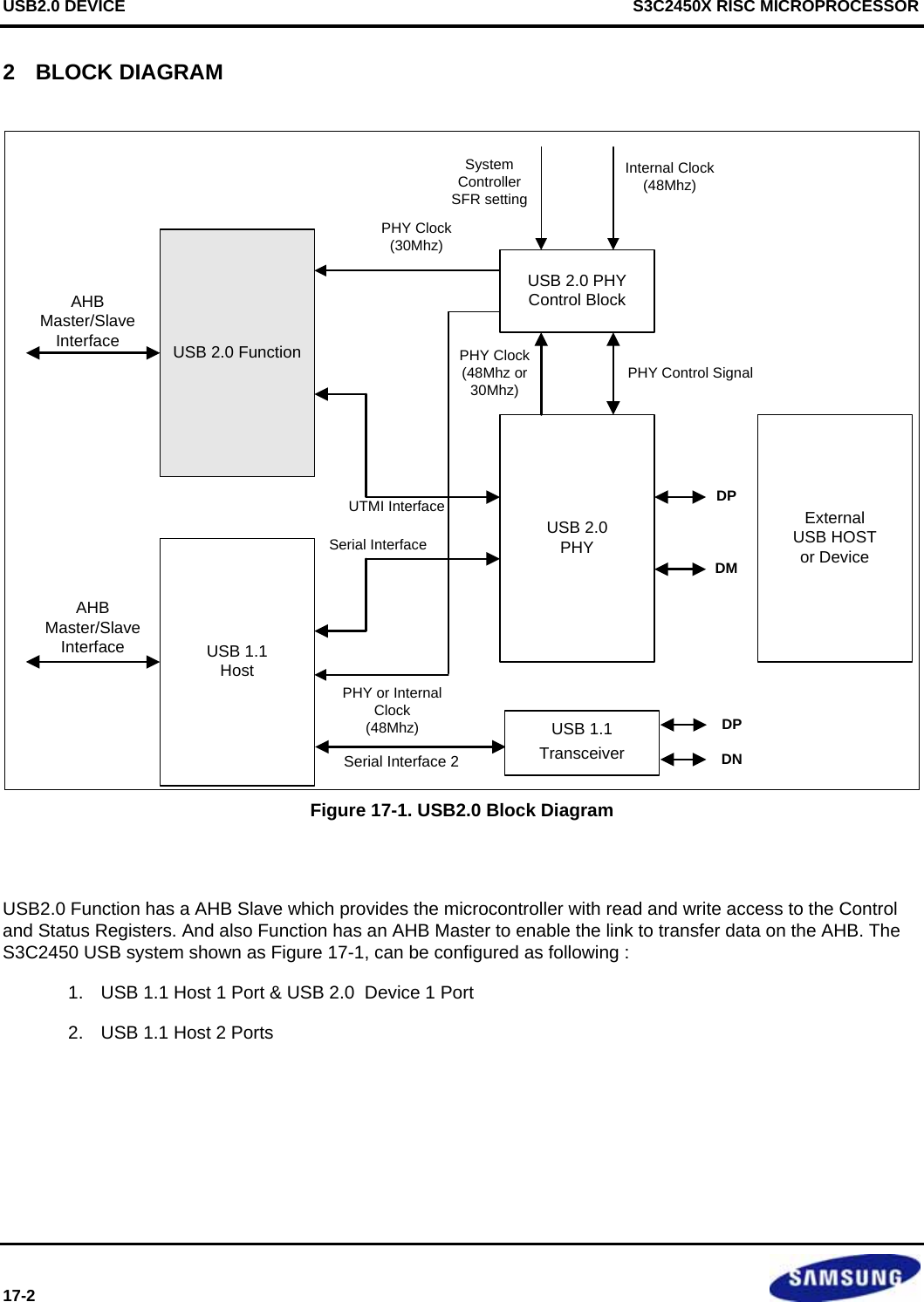
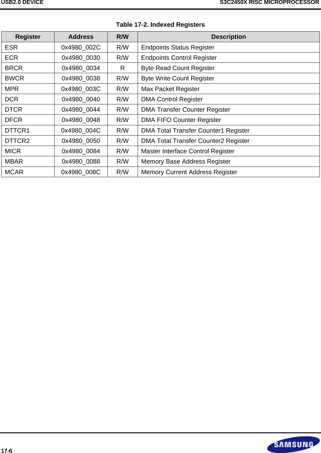
![S3C2450X RISC MICROPROCESSOR USB2.0 DEVICE 17-7 8 REGISTERS 8.1 INDEX REGISTER (IR) The index register is used for indexing a specific endpoint. In most cases, setting the index register value should precede any other operation. Register Address R/W Description Reset ValueIR 0x4980_0000 R/W Index Register 0x00 IR Bit R/W Description Initial State [31:16] − Reserved 0000 [15:4] − Reserved (Don’t write to this field) 0 INDEX [3:0] R/W Endpoint Number Select (0~6) 0000 = Endpoint0 0001 = Endpoint1 0010 = Endpoint2 0011 = Endpoint3 0100 = Endpoint4 0101 = Endpoint5 0110 = Endpoint6 0111 = Endpoint7 1000 = Endpoint8 0000](https://usermanual.wiki/Diasonic-Technology-Co/RVM-704M.Users-Manual/User-Guide-1826140-Page-405.png)
![USB2.0 DEVICE S3C2450X RISC MICROPROCESSOR 17-8 8.2 ENDPOINT INTERRUPT REGISTER (EIR) The endpoint interrupt register lets the MCU knows what endpoint generates the interrupt. The source of an interrupt could be various, but, when an interrupt is detected, the endpoint status register should be checked to identify if it’s related to specific endpoint. Clearing the bits can be accomplished by writing “1” to the bit position where the interrupt is detected. Register Address R/W Description Reset ValueEIR 0x4980_0004 R/C Endpoint Interrupt Register 0x00 EIR Bit R/W Description Initial State [31:9] − Reserved 0 EP8I [8] R/C Endpoint 8 Interrupt Flag 0 EP7I [7] R/C Endpoint 7 Interrupt Flag 0 EP6I [6] R/C Endpoint 6 Interrupt Flag 0 EP5I [5] R/C Endpoint 5 Interrupt Flag 0 EP4I [4] R/C Endpoint 4 Interrupt Flag 0 EP3I [3] R/C Endpoint 3 Interrupt Flag 0 EP2I [2] R/C Endpoint 2 Interrupt Flag 0 EP1I [1] R/C Endpoint 1 Interrupt Flag 0 EP0I [0] R/C Endpoint 0 Interrupt Flag 0](https://usermanual.wiki/Diasonic-Technology-Co/RVM-704M.Users-Manual/User-Guide-1826140-Page-406.png)
![S3C2450X RISC MICROPROCESSOR USB2.0 DEVICE 17-9 8.3 ENDPOINT INTERRUPT ENABLE REGISTER (EIER) Pairing with interrupt register, this register enables interrupt for each endpoints. Register Address R/W Description Reset ValueEIER 0x4980_0008 R/W Endpoint interrupt enable register 0x00 EIER Bit R/W Description Initial State [31:9] − Reserved EP8IE [8] R/W Endpoint 8 Interrupt Enable Flag 0 EP7IE [7] R/W Endpoint 7 Interrupt Enable Flag 0 EP6IE [6] R/W Endpoint 6 Interrupt Enable Flag 0 EP5IE [5] R/W Endpoint 5 Interrupt Enable Flag 0 EP4IE [4] R/W Endpoint 4 Interrupt Enable Flag 0 EP3IE [3] R/W Endpoint 3 Interrupt Enable Flag 0 EP2IE [2] R/W Endpoint 2 Interrupt Enable Flag 0 EP1IE [1] R/W Endpoint 1 Interrupt Enable Flag 0 EP0IE [0] R/W Endpoint 0 Interrupt Enable Flag 1 = EP0 Interrupt flag enable 0 = EP0 Interrupt flag disable 0](https://usermanual.wiki/Diasonic-Technology-Co/RVM-704M.Users-Manual/User-Guide-1826140-Page-407.png)
![USB2.0 DEVICE S3C2450X RISC MICROPROCESSOR 17-10 8.4 FUNCTION ADDRESS REGISTER (FAR) This register holds the address of USB device. Register Address R/W Description Reset ValueFAR 0x4980_000C R Function address register 0x0 FAR Bit R/W Description Initial State [31:7] − Reserved FA [6:0] R MCU can read a unique USB function address from this register. The address is transferred from USB Host through “set_address” command. 7’h0](https://usermanual.wiki/Diasonic-Technology-Co/RVM-704M.Users-Manual/User-Guide-1826140-Page-408.png)
![S3C2450X RISC MICROPROCESSOR USB2.0 DEVICE 17-11 8.5 ENDPOINT DIRECTION REGISTER (EDR) USB 2.0 Core supports IN/OUT direction control for each endpoint. This direction can’t be changed dynamically. Only by new enumeration, the direction can be altered. Since the endpoint 0 is bi-directional, there is no direction bit assigned to it. Register Address R/W Description Reset ValueEDR 0x4980_0014 R/W Endpoint direction register 0x0 EDR Bit R/W Description Initial State [31:9] − Reserved EP8DS [8] R/W Endpoint 8 Direction Select 0 EP7DS [7] R/W Endpoint 7 Direction Select 0 EP6DS [6] R/W Endpoint 6 Direction Select 0 EP5DS [5] R/W Endpoint 5 Direction Select 0 EP4DS [4] R/W Endpoint 4 Direction Select 0 EP3DS [3] R/W Endpoint 3 Direction Select 0 EP2DS [2] R/W Endpoint 2 Direction Select 0 EP1DS [1] R/W Endpoint 1 Direction Select 0 = Rx Endpoint 1 = Tx Endpoint 0 [0] − Reserved](https://usermanual.wiki/Diasonic-Technology-Co/RVM-704M.Users-Manual/User-Guide-1826140-Page-409.png)
![USB2.0 DEVICE S3C2450X RISC MICROPROCESSOR 17-12 8.6 TEST REGISTER (TR) The test register is used for the diagnostics. All bit are activated when 1 is written to and is cleared by 0 on them. Bit[3:0] are for the high speed device only. Register Address R/W Description Reset ValueTR 0x4980_0018 R/W Test register 0x0 TR Bit R/W Description Initial State [31:5] − Reserved TMD [4] R/W Test Mode. When TMD is set to 1. The core is forced into the test mode. Following TPS, TKS, TJS, TSNS bits are meaningful in test mode. 0 TPS [3] R/W Test Packets. If this bit is set, the USB repetitively transmit the test packets to Host. The test packets are explained in 7.1.20 of USB 2.0 specification. This bit can be set when TMD bit is set. 0 TKS [2] R/W Test K Select. If this bit is set, the transceiver port enters into the high-speed K state. This bit can be set when TMD bit is set. 0 TJS [1] R/W Test J Select. If this bit is set, the transceiver port enters into the high-speed J state. This bit can be set when TMD bit is set. 0 TSNS [0] R/W Test SE0 NAK Select If this bit is set, the transceiver enters into the high speed receive mode and must respond to any IN token with NAK handshake. This bit can be set when TMD bit is set. 0](https://usermanual.wiki/Diasonic-Technology-Co/RVM-704M.Users-Manual/User-Guide-1826140-Page-410.png)
![S3C2450X RISC MICROPROCESSOR USB2.0 DEVICE 17-13 8.7 SYSTEM STATUS REGISTER (SSR) This register reports operational status of the USB 2.0 Function Core, especially about error status and power saving mode status. Except the line status, every status bits in the System Status Register could be an interrupt sources. When the register is read after an interrupt due to certain system status changes, MCU should write back 1 to the corresponding bits to clear it. Register Address R/W Description Reset ValueSSR 0x4980_001C R/C Test register 0x0 SSR Bit R/W Description Initial State [31:16] − Reserved BAERR [15] R/C Byte Align Error If error interrupt enable bit of SCR register is set to 1, BAERR is set to 1 when byte alignment error is detected. 0 TMERR [14] R/C Timeout Error If error interrupt enable bit of SCR register is set to 1, TMERR is set to 1 when timeout error is detected. 0 BSERR [13] R/C Bit Stuff Error If error interrupt enable bit of SCR register is set to 1, BSERR is set to 1 when bit stuff error is detected. 0 TCERR [12] R/C Token CRC Error If error interrupt enable bit of SCR register is set to 1, BSERR is set to 1 when CRC error in token packet is detected. 0 DCERR [11] R/C Data CRC Error If error interrupt enable bit of SCR register is set to 1, DCERR is set to 1 when CRC error in data packet is detected. 0 EOERR [10] R/C EB OVERRUN Error If error interrupt enable bit of SCR register is set to 1, EOERR is set to 1 when EB overrun error in transceiver is detected. 0 [9:8] − Reserved TBM [7] R/C Toggle Bit Mismatch. If error interrupt enable bit of SCR register is set to 1, TBM is set to 1 when Toggle mismatch is detected. 0 DP [6] R DP Data Line State DP informs the status of D+ Line 0 DM [5] R DM Data Line State DM informs the status of D- Line 0 HSP [4] R Host Speed 0 = Full Speed 1 = High Speed 0](https://usermanual.wiki/Diasonic-Technology-Co/RVM-704M.Users-Manual/User-Guide-1826140-Page-411.png)
![USB2.0 DEVICE S3C2450X RISC MICROPROCESSOR 17-14 SSR Bit R/W Description Initial StateSDE [3] R/C Speed Detection End. SDE is set by the core when the HS Detect Handshake process is ended. 0 HFRM [2] R/C Host Forced Resume. HFRM is set by the core in suspend state when host sends resume signaling. 0 HFSUSP [1] R/C Host Forced Suspend HFSUSP is set by the core when the SUSPEND signaling from host is detected. 0 HFRES [0] R/C Host Forced Reset. HFRES is set by the core when the RESET signaling from host is detected. 0](https://usermanual.wiki/Diasonic-Technology-Co/RVM-704M.Users-Manual/User-Guide-1826140-Page-412.png)
![S3C2450X RISC MICROPROCESSOR USB2.0 DEVICE 17-15 8.8 SYSTEM CONTROL REGISTER (SCR) This register enables top-level control of the core. MCU should access this register for controls such as Power saving mode enable/disable. Register Address R/W Description Reset ValueSCR 0x4980_0020 R/W System control register 0x0 SCR Bit R/W Description Initial State [31:15] − Reserved DTZIEN [14] R/W DMA Total Counter Zero Interrupt Enable 0 = Disable 1 = Enable When set to 1, DMA total counter zero interrupt is generated. 0 [13] − Reserved DIEN [12] R/W DUAL Interrupt Enable 0 = Disable 1 = Enable When set to 1, Interrupt is activated until Interrupt source is cleared. 0 [11:9] − Reserved EIE [8] R/W Error Interrupt Enable This bit must be set to 1 to enable error interrupt. 0 SPDCEN [7] R/W Speed detection Control Enable 0 = Disable 1 = Enable 0 SPDEN [6] R/W Speed Detect End Interrupt Enable When set to 1, Speed detection interrupt is generated. 0 [5] − Reserved [4] − Should be zero 0 SPDC [3] R/W Speed detection Control Software can reset Speed detection Logic through this bit. This bit is used to control speed detection process in case of System with a long initial time. 0 = Enable 1 = Disable 0 MFRM [2] R/W Resume by MCU If this bit is set, the suspended core generates a resume signal. This bit is set when MCU writes 1. This bit is cleared when MCU writes 0. 0 HSUSPE [1] R/W Suspend Enable When set to 1, core can respond to the suspend signaling by USB host. 0 HRESE [0] R/W Reset Enable When set to 1, core can respond to the reset signaling by USB host. 0](https://usermanual.wiki/Diasonic-Technology-Co/RVM-704M.Users-Manual/User-Guide-1826140-Page-413.png)
![USB2.0 DEVICE S3C2450X RISC MICROPROCESSOR 17-16 8.9 EP0 STATUS REGISTER (EP0SR) This register stores status information of the Endpoint 0. These status information are set automatically by the core when corresponding conditions are met. After reading the bits, MCU should write 1 to clear them. Register Address R/W Description Reset ValueEP0SR 0x4980_0024 R/W EP0 status register 0x0 EP0SR Bit R/W Description Initial State [31:7] − Reserved LWO [6] R Last Word Odd Low informs that the last word of a packet in FIFO has an invalid upper byte. This bit is cleared automatically after the MCU reads it from the FIFO. 0 [5] − Reserved SHT [4] R/C Stall Handshake Transmitted. SHT informs that STALL handshake due to stall condition is sent to Host. This bit is an interrupt source. This bit is cleared when the MCU writes 1. 0 [3:2] − Reserved TST [1] R/C Tx successfully received. TST is set by core after core sends TX data to Host and receives ACK successfully. TST is one of the interrupt sources. 0 RSR [0] R/C Rx successfully received. RSR is set by core after core receives error free packet from Host and sent ACK back to Host successfully. RSR is one of the interrupt sources. 0](https://usermanual.wiki/Diasonic-Technology-Co/RVM-704M.Users-Manual/User-Guide-1826140-Page-414.png)
![S3C2450X RISC MICROPROCESSOR USB2.0 DEVICE 17-17 8.10 EP0 CONTROL REGISTER (EP0CR) EP0 control register is used for the control of endpoint 0. Controls such as enabling ep0 related interrupts and toggle controls can be handled by EP0 control register. Register Address R/W Description Reset ValueEP0CR 0x4980_0028 R/W EP0 control register 0x0 EP0CR Bit R/W Description Initial State [31:2] − Reserved ESS [1] R/W Endpoint Stall Set ESS is set by MCU when it intends to send STALL handshake to Host. This bit is cleared when the MCU writes 0 on it. ESS is needed to be set 0 after MCU writes 1 on it. 0 TZLS [0] R/W Tx Zero Length Set. TZLS is set by MCU when it intends to send Tx zero length data to Host. TZLS is useful for core Test. TZLS can be managed when Tx Test Enable (TTE) bit is set. This bit is cleared when the MCU writes 0 on it 0](https://usermanual.wiki/Diasonic-Technology-Co/RVM-704M.Users-Manual/User-Guide-1826140-Page-415.png)
![USB2.0 DEVICE S3C2450X RISC MICROPROCESSOR 17-18 8.11 ENDPOINT# BUFFER REGISTER (EP#BR) The buffer register is used to hold data for TX/RX transfer. Register Address R/W Description Reset ValueEP0BR 0x4980_0060 R/W EP0 Buffer Register 0x0 EP1BR 0x4980_0064 R/W EP1 Buffer Register 0x0 EP2BR 0x4980_0068 R/W EP2 Buffer Register 0x0 EP3BR 0x4980_006C R/W EP3 Buffer Register 0x0 EP4BR 0x4980_0070 R/W EP4 Buffer Register 0x0 EP5BR 0x4980_0074 R/W EP5 Buffer Register 0x0 EP6BR 0x4980_0078 R/W EP6 Buffer Register 0x0 EP7BR 0x4980_007C R/W EP7 Buffer Register 0x0 EP8BR 0x4980_0080 R/W EP8 Buffer Register 0x0 EP#BR Bit R/W Description Initial State [31:16] − Reserved [15:0] R/W Buffer register holds TX/RX data between MCU and the core 16hX](https://usermanual.wiki/Diasonic-Technology-Co/RVM-704M.Users-Manual/User-Guide-1826140-Page-416.png)
![S3C2450X RISC MICROPROCESSOR USB2.0 DEVICE 17-19 8.12 ENDPOINT STATUS REGISTER (ESR) The endpoint status register reports current status of an endpoint (except EP0) to the MCU Register Address R/W Description Reset ValueESR 0x4980_002C R/W Endpoint status register 0x0 ESR Bit R/W Description Initial State [31:12] Reserved FPID [11] R/W First OUT Packet interrupt Disable in OUT DMA operation. First Received OUT packet generates interrupt if this bit is disabled and DEN in DMA control register is enabled 0 = Disable 1 = Enable 0 OSD [10] R/C OUT Start DMA Operation. OSD is set when First OUT packet is received after Registers related DMA Operation are set. 0 DTCZ [9] R/C DMA Total Count Zero DTCZ is set when DMA Operation Total Counter reach to 0. This bit is cleared when the MCU writes 1 on it. 0 SPT [8] R/C Short Packet Received. SPT informs that OUT endpoint receives short packet during OUT DMA Operation. This bit is cleared when the MCU writes 1 on it. 0 DOM [7] R Dual Operation Mode DOM is set when the max packet size of corresponding endpoint is equal to a half FIFO size. This bit is read only. Endpoint0 does not support dual mode. 0 FFS [6] R/C FIFO Flushed. FFS informs that FIFO is flushed. This bit is an interrupt source. This bit is cleared when the MCU clears FLUSH bit in Endpoint Control Register. 0 FSC [5] R/C Function Stall Condition. FSC informs that STALL handshake due to functional stall condition is sent to Host. This bit is set when endpoint stall set bit is set by the MCU. This bit is cleared when the MCU writes 1 on it. 0 LWO [4] R Last Word Odd. Low informs that the lower byte of last word is only valid. This bit is automatically cleared after the MCU reads packet data received Host. 0](https://usermanual.wiki/Diasonic-Technology-Co/RVM-704M.Users-Manual/User-Guide-1826140-Page-417.png)
![USB2.0 DEVICE S3C2450X RISC MICROPROCESSOR 17-20 ESR Bit R/W Description Initial StatePSIF [3:2] R Packet Status In FIFO. 00 = No packet in FIFO 01 = One packet in FIFO 10 = Two packet in FIFO 11 = Invalid value 0 TPS [1] R/C Tx Packet Success TPS is used for Single or Dual transfer mode. TPS is activated when one packet data in FIFO was successfully transferred to Host and received ACK from Host. This bit should be cleared by writing 1 on it after being read by the MCU. 0 RPS [0] R Rx Packet Success. RPS is used for Single or Dual transfer mode. RPS is activated when the FIFO has a packet data to receive. RPS is automatically cleared when MCU reads all packets (one or two) from FIFO. MCU can identify the packet size through byte read count register (BRCR). 0](https://usermanual.wiki/Diasonic-Technology-Co/RVM-704M.Users-Manual/User-Guide-1826140-Page-418.png)
![S3C2450X RISC MICROPROCESSOR USB2.0 DEVICE 17-21 8.13 ENDPOINT CONTROL REGISTER (ECR) The endpoint control register is useful for controlling an endpoint both in normal operation and test case. Putting an endpoint in specific operation mode can be accomplished through the endpoint control register. Register Address R/W Description Reset ValueECR 0x4980_0030 R/W Endpoint Control Register 0x0 ECR Bit R/W Description Initial State [31:13] − Reserved INPKTHLD [12] R/W The MCU can control Tx FIFO status through this bit. If this bit is set to one, USB does not send IN data to Host. 0 = The USB can send IN data to Host according to IN FIFO status(normal operation) 1 = The USB sends NAK handshake to Host regardless of IN FIFO status. 0 OUTPKTHLD [11] R/W The MCU can control Rx FIFO Status through this bit. If this bit is set to one, USB does not accept OUT data from Host. 0 = The USB can accept OUT data from Host according to OUT FIFO status(normal operation) 1 = The USB does not accept OUT data from Host. 0 [10:8] − Reserved DUEN [7] R/W Dual FIFO mode Enable 0 = Dual Disable(Single mode) 1 = Dual Enable 0 FLUSH [6] R/W FIFO Flush FIFO is flushed when this bit is set to 1. This bit is automatically cleared after MCU writes 1. 0 [5:2] − Reserved ESS [1] R/W Endpoint Stall Set ESS is set by the MCU when the MCU intends to send STALL handshake to Host. This bit is cleared when the MCU writes 0 in it. 0 IEMS [0] R/W Interrupt Endpoint Mode Set IEMS determines the transfer type of an endpoint. 0 = Interrupt Transfer mode Disable 1 = Interrupt Transfer mode Enable 0](https://usermanual.wiki/Diasonic-Technology-Co/RVM-704M.Users-Manual/User-Guide-1826140-Page-419.png)
![USB2.0 DEVICE S3C2450X RISC MICROPROCESSOR 17-22 8.14 BYTE READ COUNT REGISTER (BRCR) The byte read count register keeps byte (half word) counts of a RX packet from USB host. Register Address R/W Description Reset ValueBRCR 0x4980_0034 R Byte Read Count Register 0x0 BRCR Bit R/W Description Initial State [31:10] − Reserved RDCNT [9:0] R FIFO Read Byte Count[9:0] RDCNT is read only. The BRCR inform the amount of received data from host. In 16-bit Interface, RDCNT informs the amount of data in half word (16-bit) unit. Through the LWO bit of EP0SR, the MCU can determine valid byte in last data word. 10’h](https://usermanual.wiki/Diasonic-Technology-Co/RVM-704M.Users-Manual/User-Guide-1826140-Page-420.png)
![S3C2450X RISC MICROPROCESSOR USB2.0 DEVICE 17-23 8.15 BYTE WRITE COUNT REGISTER (BWCR) The byte write count register keeps the byte (half word) count value of a TX packet from MCU. The counter value will be used to determine the end of TX packet. Register Address R/W Description Reset ValueBWCR 0x4980_0038 R/W Byte Write Count Register 0x0 BWCR Bit R/W Description Initial State [31:10] − Reserved WRCNT [9:0] R/W Through BWCR, the MCU must load the byte counts of a TX data packet to the core. The core uses this count value to determine the end of packet. The count value to this register must be less than MAXP. 10’h](https://usermanual.wiki/Diasonic-Technology-Co/RVM-704M.Users-Manual/User-Guide-1826140-Page-421.png)
![USB2.0 DEVICE S3C2450X RISC MICROPROCESSOR 17-24 8.16 MAX PACKET REGISTER (MPR) The byte write count register keeps the byte (half word) count value of a TX packet from MCU. The counter value will be used to determine the end of TX packet. Register Address R/W Description Reset ValueMPR 0x4980_003C R/W MAX Packet Register 0x0 MPR Bit R/W Description Initial State [31:11] − Reserved MAXP [10:0] R/W MAX Packet [10:0] The max packet size of each endpoint is determined by MAX packet register. The range of max packet is from 0 to 1024 bytes. 000_0000_0000 = Max Packet 0 byte. 000_0000_1000 = Max Packet 8 bytes. 000_0001_0000 = Max Packet 16 bytes. 000_0010_0000 = Max Packet 32 bytes. 000_0100_0000 = Max Packet 64 bytes. 000_1000_0000 = Max Packet 128 bytes. 001_0000_0000 = Max Packet 256 bytes. 010_0000_0000 = Max Packet 512 bytes. 100_0000_0000 = Max Packet 1024 bytes. 11’h0](https://usermanual.wiki/Diasonic-Technology-Co/RVM-704M.Users-Manual/User-Guide-1826140-Page-422.png)
![S3C2450X RISC MICROPROCESSOR USB2.0 DEVICE 17-25 8.17 DMA CONTROL REGISTER (DCR) The AHB Master Operation is controlled by the programming DMA Control Register and DMA IF Control Register. Register Address R/W Description Reset ValueDCR 0x4980_0040 R/W DMA Control Register 0x0 DCR Bit R/W Description Initial State [31:6] − Reserved ARDRD [5] R/W Auto Rx DMA Run set disable. 0 = Set 1 = Disable This bit is cleared when DMA operation is ended. 0 FMDE [4] R/W Burst Mode Enable. This bit is used to run Burst Mode DMA Operation. 0 = Burst mode disable 1 = Burst mode enable 0 DMDE [3] R/W Demand Mode DMA Enable. This bit is used to run Demand mode DMA operation. 0 = Demand mode disable. 1 = Demand mode enable. 0 TDR [2] R/W Tx DMA Operation Run This bit is used to set start DMA operation for Tx Endpoint (IN endpoint) 0 = DMA operation stop 1 = DMA operation run 0 RDR [1] R/W Rx DMA Operation Run This bit is used to start DMA operation for Rx Endpoint (OUT endpoint). This bit is automatically set when USB receives OUT packet data and DEN bit is set to 1 and ARDRD bit is set to 0. To operate DMA operation after OUT packet data received, MCU must set RDR to 1. 0 = DMA operation stop. 1 = DMA operation run. 0 DEN [0] R/W DMA Operation Mode Enable This bit is used to set the DMA Operation mode 0 = Interrupt Operation mode 1 = DMA Operation mode 0](https://usermanual.wiki/Diasonic-Technology-Co/RVM-704M.Users-Manual/User-Guide-1826140-Page-423.png)
![USB2.0 DEVICE S3C2450X RISC MICROPROCESSOR 17-26 8.18 DMA TRANSFER COUNTER REGISTER (DTCR) The byte write count register keeps the byte (half word) count value of a TX packet from MCU. The counter value will be used to determine the end of TX packet. Register Address R/W Description Reset ValueDTCR 0x4980_0044 R/W DMA Transfer Counter Register 0x0 MTCR Bit R/W Description Initial State [31:11] Reserved DTCR [10:0] R/W To operate single mode transfer, DTCR is needed to be set 11’h0002. In case of Burst mode, the MCU should set max packet value. 11’h0](https://usermanual.wiki/Diasonic-Technology-Co/RVM-704M.Users-Manual/User-Guide-1826140-Page-424.png)
![S3C2450X RISC MICROPROCESSOR USB2.0 DEVICE 17-27 8.19 DMA FIFO COUNTER REGISTER (DFCR) This register has the byte number of data per DMA operation. The max packet size is loaded in this register. Register Address R/W Description Reset ValueDFCR 0x4980_0048 R/W DMA FIFO Counter Register 0x0 MFCR Bit R/W Description Initial State [31:12] − Reserved DFCR [11:0] R/W In case of OUT Endpoint, the size value of received packet will be loaded in this register automatically when Rx DMA Run is enabled. In case of IN Endpoint, the MCU should set max packet value. 12’h0](https://usermanual.wiki/Diasonic-Technology-Co/RVM-704M.Users-Manual/User-Guide-1826140-Page-425.png)
![USB2.0 DEVICE S3C2450X RISC MICROPROCESSOR 17-28 8.20 DMA TOTAL TRANSFER COUNTER REGISTER 1/2 (DTTCR 1/2) This register has the total byte number of data to transfer using DMA Interface. When this counter register value is zero, DMA operation is ended. Register Address R/W Description Reset ValueDTTCR1 DTTCR2 0x4980_004C 0x4980_0050 R/W DMA Total Transfer Counter Register 1/2 0x0 MTTCR# Bit R/W Description Initial State [31:16] Reserved DTTCR [15:0] R/W This register should have total byte size to be transferred using DMA Interface. DMA Total Transfer Counter1 : Low half word value DMA Total Transfer Counter2 : High half word value. The max value is up to 2^32 16’h0](https://usermanual.wiki/Diasonic-Technology-Co/RVM-704M.Users-Manual/User-Guide-1826140-Page-426.png)
![S3C2450X RISC MICROPROCESSOR USB2.0 DEVICE 17-29 8.21 DMA INTERFACE CONTROL REGISTER (DICR) The AHB Master Operation is controlled by the programming DMA Control Register and DMA IF Control Register. Register Address R/W Description Reset ValueDICR 0x4980_0084 R/W DMA Interface Counter Register 0x0 DICR Bit R/W Description Initial StateReserved [31:4] − Reserved 0 RELOAD_ MBAR [4] R/W Select Reload Condiion 0 = Every end of Full DMA operation 1 = Every Packet transfer. 0 Reserved [3:2] Reserved 0 MAX_BURST [1:0] R/W Max Burst Length 00 = Single transfer 01 = 4-beat incrementing burst transfer(INCR4) 10 = 8-beat incrementing burst transfer(INCR8) 11 = 16-beat incrementing burst transfer(INCR16) 00](https://usermanual.wiki/Diasonic-Technology-Co/RVM-704M.Users-Manual/User-Guide-1826140-Page-427.png)
![USB2.0 DEVICE S3C2450X RISC MICROPROCESSOR 17-30 8.22 MEMORY BASE ADDRESS REGISTER (MBAR) Register Address R/W Description Reset ValueMBAR 0x4980_0088 R/W Memory Base Address Register 0x0 MBAR# Bit R/W Description Initial StateMBAR [31:0] R/W This register should have memory base address to be transferred using DMA Interface. 32’h0](https://usermanual.wiki/Diasonic-Technology-Co/RVM-704M.Users-Manual/User-Guide-1826140-Page-428.png)
![S3C2450X RISC MICROPROCESSOR USB2.0 DEVICE 17-31 8.23 MEMORY CURRENT ADDRESS REGISTER (MCAR) Register Address R/W Description Reset ValueMCAR 0x4980_008C R Memory Current Address Register 0x0 MCAR# Bit R/W Description Initial StateMCAR [31:0] R This register should have memory current address to be transferred using DMA Interface. 8.24 BURST FIFO CONTROL REGISTER(FCON) Register Address R/W Description Reset ValueFCON 0x4980_0100 R/W Burst DMA transfer Control 0x0 MBAR# Bit R/W Description Initial StateReserved [31:9] R/W Reserved 000000 DMAEN [8] R/W DMA enable 0 Rreserved [7:5] R/W Reserved 000 TF_CLR [4] R/W TX fifo clear 0 Reserved [3:1] R/W Reserved 000 RF_CLR [0] R/W RX fifo clear 0 8.25 BURST FIFO STATUS REGISTER(FSTAT) Register Address R/W Description Reset ValueFSTAT 0x4980_0104 R/W Burst DMA transfer Status 0x0 FSTAT Bit R/W Description Initial StateReserved [31:14] R Reserved TF_FULL [13] R TX FIFO Full 0 TF_CNT [12:8] R # of data in TX fifo 0 Reserved [7:6] R Reserved 0 RF_FULL [5] R RX FIFO Full 0 RF_CNT [4:0] R # of data in RX fifo 0](https://usermanual.wiki/Diasonic-Technology-Co/RVM-704M.Users-Manual/User-Guide-1826140-Page-429.png)
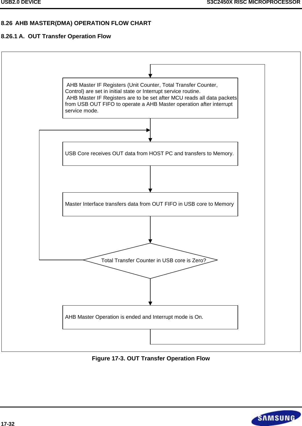
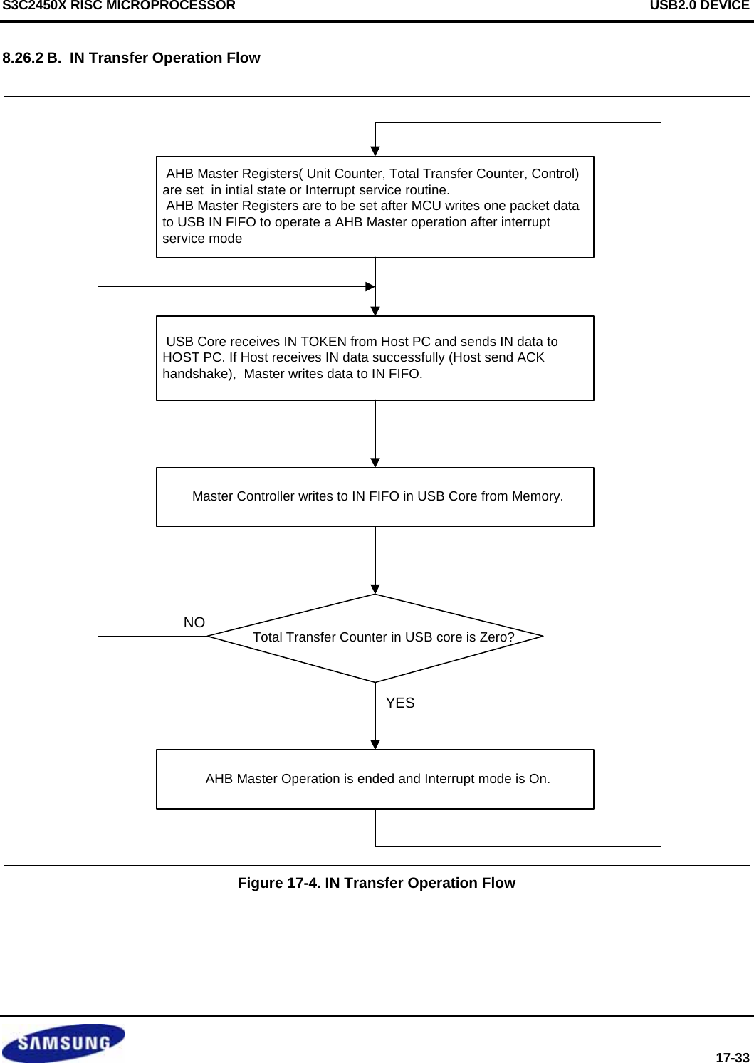

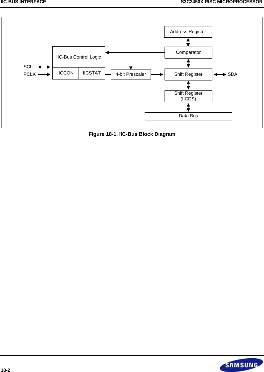
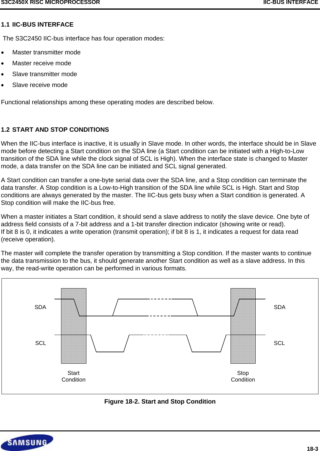
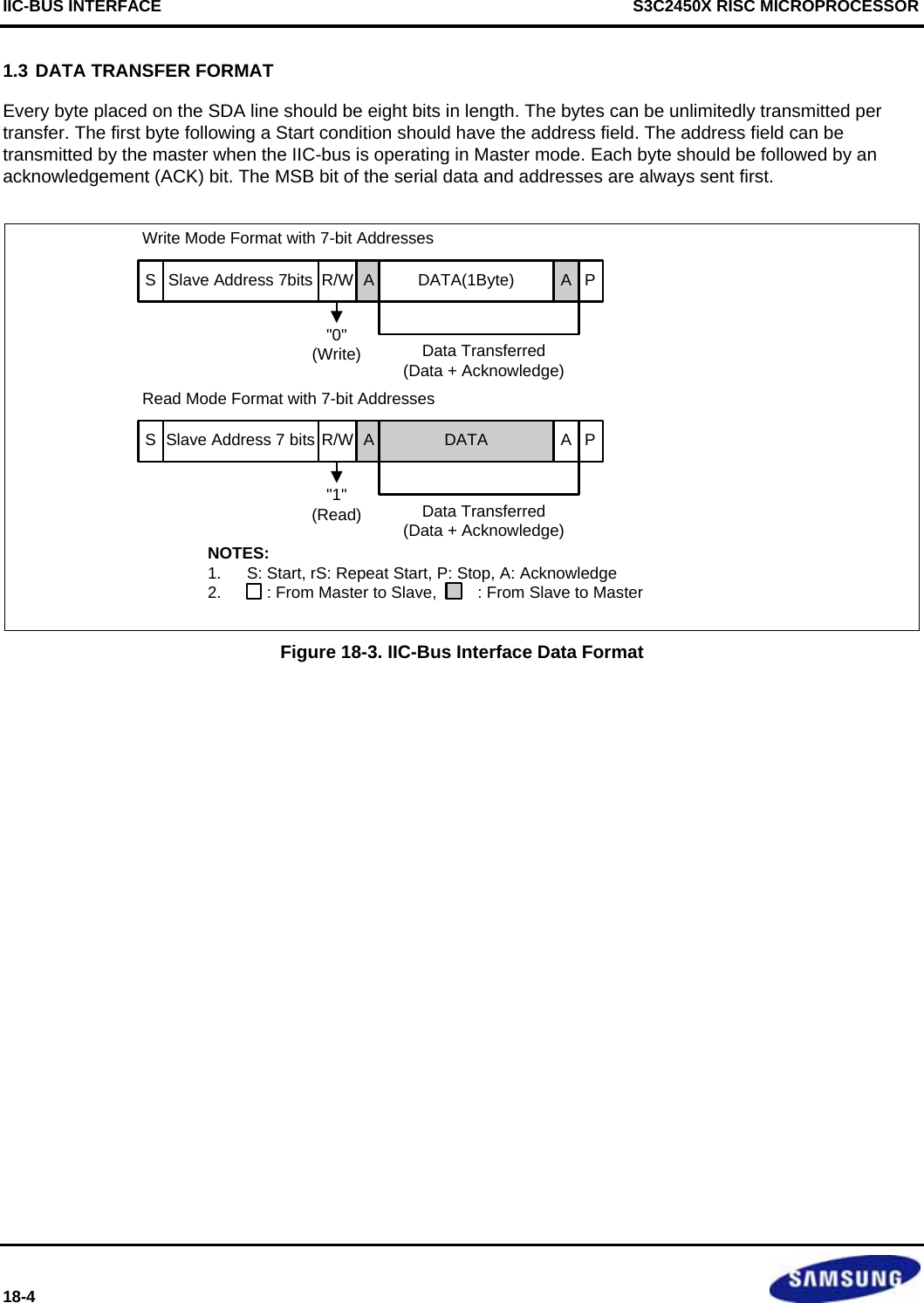
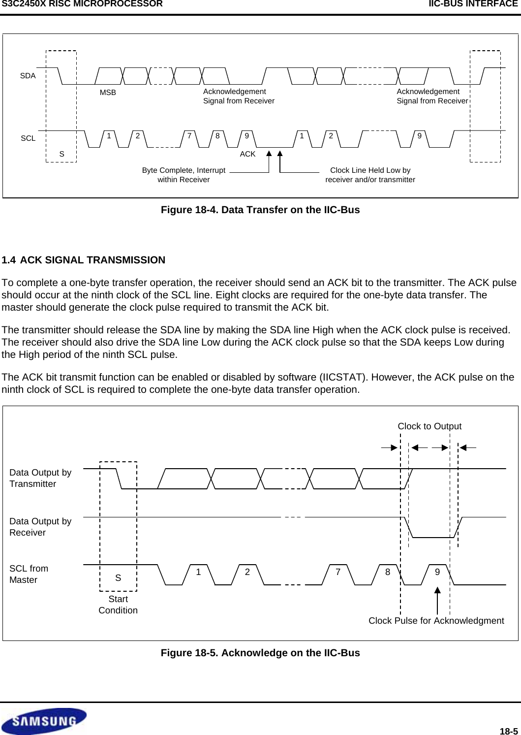
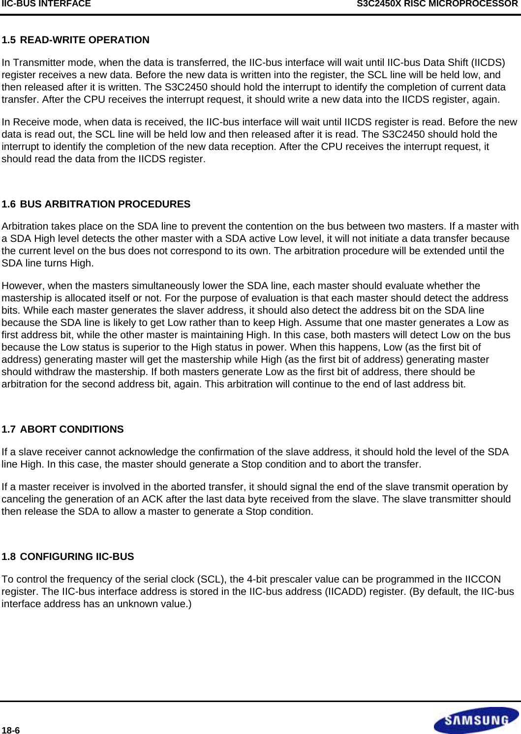
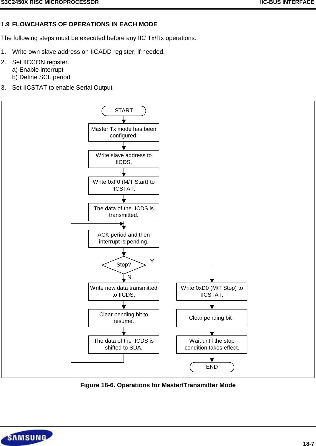
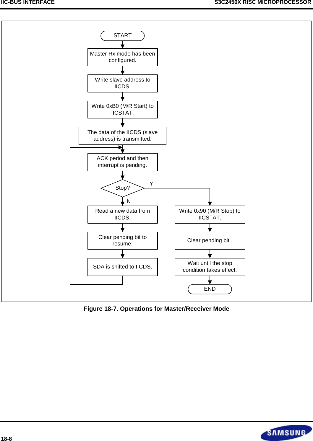
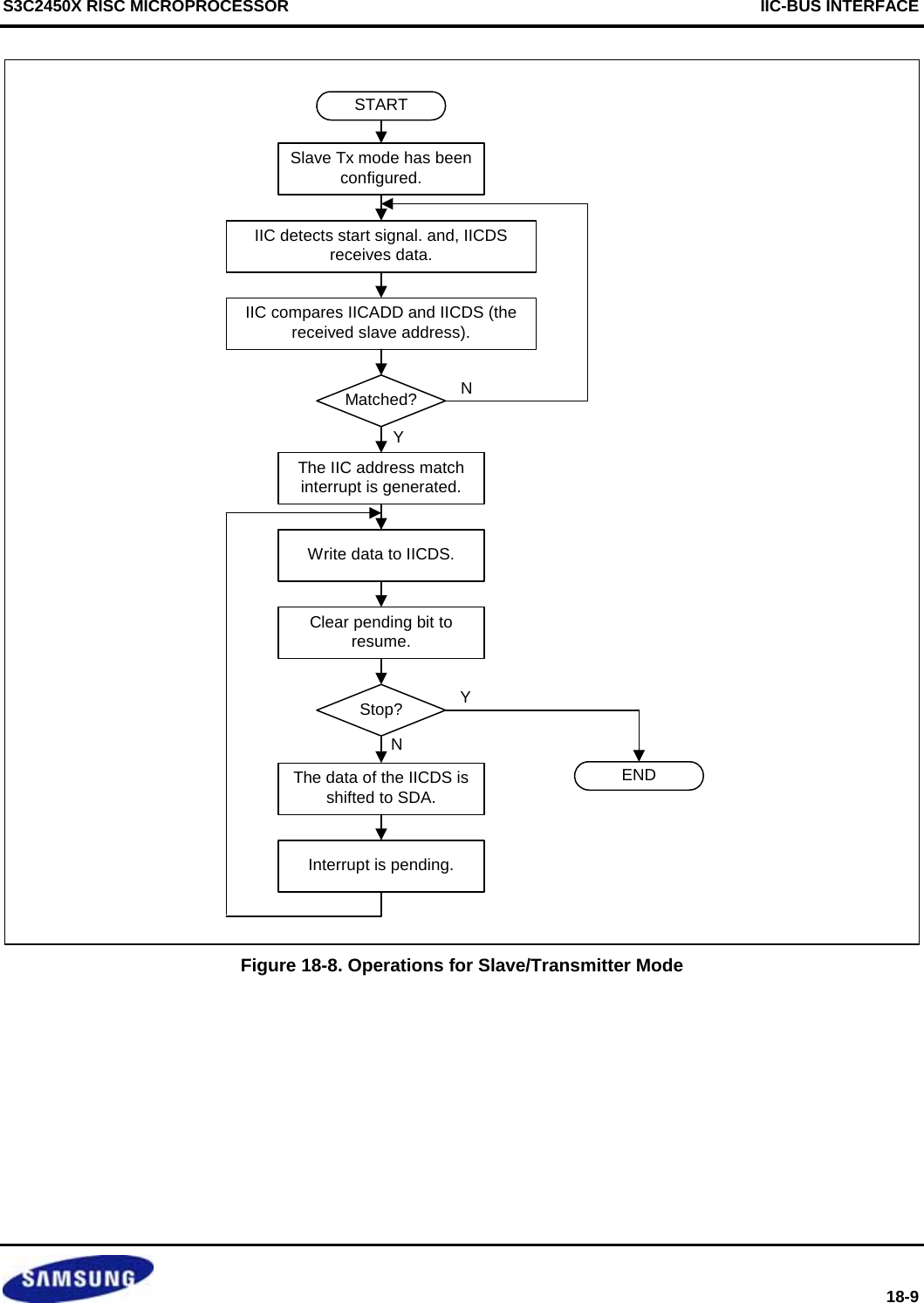
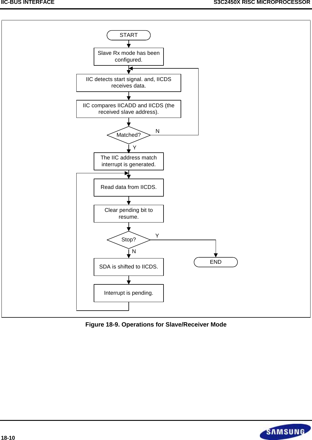
![S3C2450X RISC MICROPROCESSOR IIC-BUS INTERFACE 18-11 2 IIC-BUS INTERFACE SPECIAL REGISTERS 2.1 MULTI-MASTER IIC-BUS CONTROL (IICCON) REGISTER Register Address R/W Description Reset ValueIICCON0 0x54000000 R/W IIC0-Bus control register 0x0X IICCON1 0x54000100 R/W IIC1-Bus control register 0x0X IICCON0 IICCON1 Bit Description Initial StateAcknowledge generation (note 1) [7] IIC-bus acknowledge enable bit. 0 = Disable 1 = Enable In Tx mode, the IICSDA is free in the ack time. In Rx mode, the IICSDA is L in the ack time. 0 Tx clock source selection [6] Source clock of IIC-bus transmit clock prescaler selection bit. 0 = IICCLK = PCLK /16 1 = IICCLK = PCLK /512 0 Tx/Rx Interrupt (note 5) [5] IIC-Bus Tx/Rx interrupt enable/disable bit. 0 = Disable, 1 = Enable 0 Interrupt pending flag (note 2) (note 3) [4] IIC-bus Tx/Rx interrupt pending flag. This bit cannot be written to 1. When this bit is read as 1, the IICSCL is tied to L and the IIC is stopped. To resume the operation, clear this bit as 0. 0 = 1) No interrupt pending (when read). 2) Clear pending condition & Resume the operation (when write). 1 = 1) Interrupt is pending (when read) 2) N/A (when write) 0 Transmit clock value (note 4) [3:0] IIC-Bus transmit clock prescaler. IIC-Bus transmit clock frequency is determined by this 4-bit prescaler value, according to the following formula: Tx clock = IICCLK/(IICCON[3:0]+1). Undefined NOTES: 1. Interfacing with EEPROM, the ack generation may be disabled before reading the last data in order to generate the STOP condition in Rx mode. 2. An IIC-bus interrupt occurs 1) when a 1-byte transmits or receives operation is completed, 2) when a general call or a slave address match occurs, or 3) if bus arbitration fails. 3. To adjust the setup time of SDA before SCL rising edge, IICDS has to be written before clearing the IIC interrupt pending bit. 4. IICCLK is determined by IICCON[6]. Tx clock can vary by SCL transition time. When IICCON[6]=0, IICCON[3:0]=0x0 or 0x1 is not available. 5. If the IICCON[5]=0, IICCON[4] does not operate correctly. So, It is recommended that you should set IICCON[5]=1, although you does not use the IIC interrupt.](https://usermanual.wiki/Diasonic-Technology-Co/RVM-704M.Users-Manual/User-Guide-1826140-Page-443.png)
![IIC-BUS INTERFACE S3C2450X RISC MICROPROCESSOR 18-12 2.2 MULTI-MASTER IIC-BUS CONTROL/STATUS (IICSTAT) REGISTER Register Address R/W Description Reset ValueIICSTAT0 0x54000004 R/W IIC0-Bus control/status register 0x0 IICSTAT1 0x54000104 R/W IIC1-Bus control/status register 0x0 IICSTAT0 IICSTAT1 Bit Description Initial StateMode selection [7:6] IIC-bus master/slave Tx/Rx mode select bits. 00 = Slave receive mode 01 = Slave transmit mode 10 = Master receive mode 11 = Master transmit mode 00 Busy signal status / START STOP condition [5] IIC-Bus busy signal status bit. 0 = read) Not busy (when read) write) STOP signal generation 1 = read) Busy (when read) write) START signal generation. The data in IICDS will be transferred automatically just after the start signal. 0 Serial output [4] IIC-bus data output enable/disable bit. 0 = Disable Rx/Tx 1 = Enable Rx/Tx 0 Arbitration status flag [3] IIC-bus arbitration procedure status flag bit. 0 = Bus arbitration successful 1 = Bus arbitration failed during serial I/O 0 Address-as-slave status flag [2] IIC-bus address-as-slave status flag bit. 0 = Cleared after reading of IICSTAT register 1 = Received slave address matches the address value in the IICADD 0 Address zero status flag [1] IIC-bus address zero status flag bit. 0 = Cleared when START/STOP condition was detected 1 = Received slave address is 00000000b. 0 Last-received bit status flag [0] IIC-bus last-received bit status flag bit. 0 = Last-received bit is 0 (ACK was received). 1 = Last-received bit is 1 (ACK was not received). 0](https://usermanual.wiki/Diasonic-Technology-Co/RVM-704M.Users-Manual/User-Guide-1826140-Page-444.png)
![S3C2450X RISC MICROPROCESSOR IIC-BUS INTERFACE 18-13 2.3 MULTI-MASTER IIC-BUS ADDRESS (IICADD) REGISTER Register Address R/W Description Reset ValueIICADD0 0x54000008 R/W IIC0-Bus address register 0xXX IICADD1 0x54000108 R/W IIC1-Bus address register 0xXX IICADD0 IICADD1 Bit Description Initial StateSlave address [7:0] 7-bit slave address, latched from the IIC-bus. When serial output enable = 0 in the IICSTAT, IICADD is write-enabled. The IICADD value can be read any time, regardless of the current serial output enable bit (IICSTAT) setting. Slave address : [7:1] Not mapped : [0] XXXXXXXX 2.4 MULTI-MASTER IIC-BUS TRANSMIT/RECEIVE DATA SHIFT (IICDS) REGISTER Register Address R/W Description Reset ValueIICDS0 0x5400000C R/W IIC0-Bus transmit/receive data shift register 0xXX IICDS1 0x5400010C R/W IIC1-Bus transmit/receive data shift register 0xXX IICDS0 IICDS1 Bit Description Initial StateData shift [7:0] 8-bit data shift register for IIC-bus Tx/Rx operation. When serial output enable = 1 in the IICSTAT, IICDS is write-enabled. The IICDS value can be read any time, regardless of the current serial output enable bit (IICSTAT) setting. XXXXXXXX](https://usermanual.wiki/Diasonic-Technology-Co/RVM-704M.Users-Manual/User-Guide-1826140-Page-445.png)
![IIC-BUS INTERFACE S3C2450X RISC MICROPROCESSOR 18-14 2.5 MULTI-MASTER IIC-BUS LINE CONTROL(IICLC) REGISTER Register Address R/W Description Reset ValueIICLC0 0x54000010 R/W IIC0-Bus multi-master line control register 0x00 IICLC1 0x54000110 R/W IIC1-Bus multi-master line control register 0x00 IICLC0 IICLC1 Bit Description Initial StateFilter enable [2] IIC-bus filter enable bit. When SDA port is operating as input, this bit should be High. This filter can prevent from occurred error by a glitch during double of PCLK time. 0 = Filter disable 1 = Filter enable 0 SDA output delay [1:0] IIC-Bus SDA line delay length selection bits. SDA line is delayed as following clock time(PCLK) 00 = 0 clocks 01 = 5 clocks 10 = 10 clocks 11 = 15 clocks 00](https://usermanual.wiki/Diasonic-Technology-Co/RVM-704M.Users-Manual/User-Guide-1826140-Page-446.png)
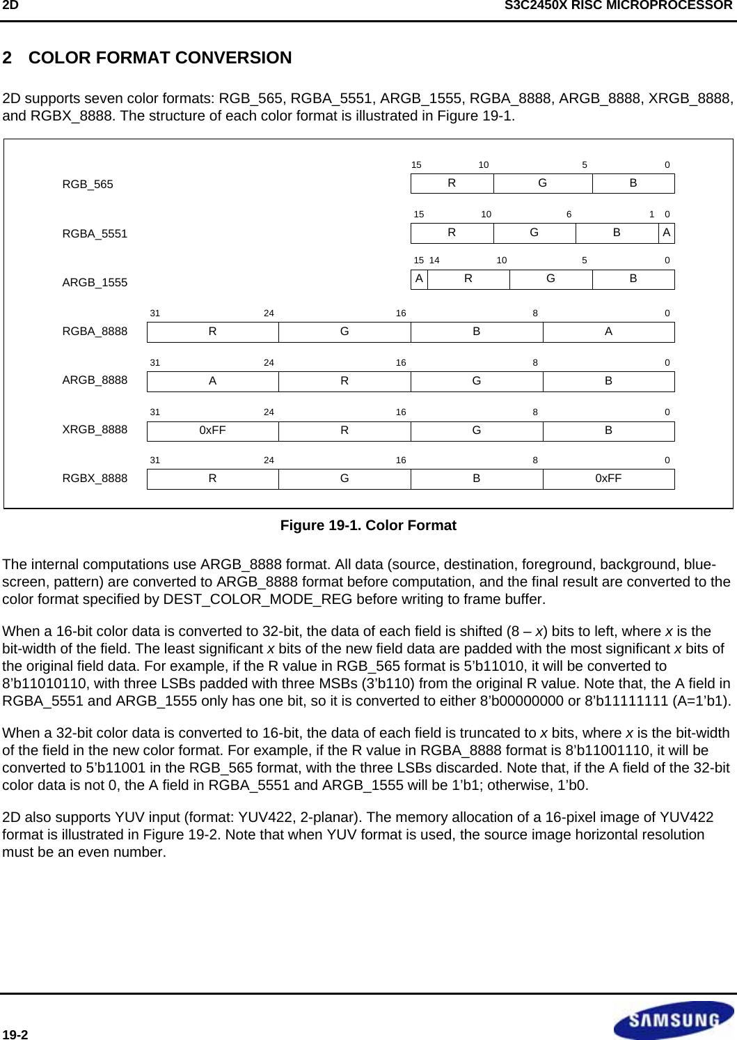
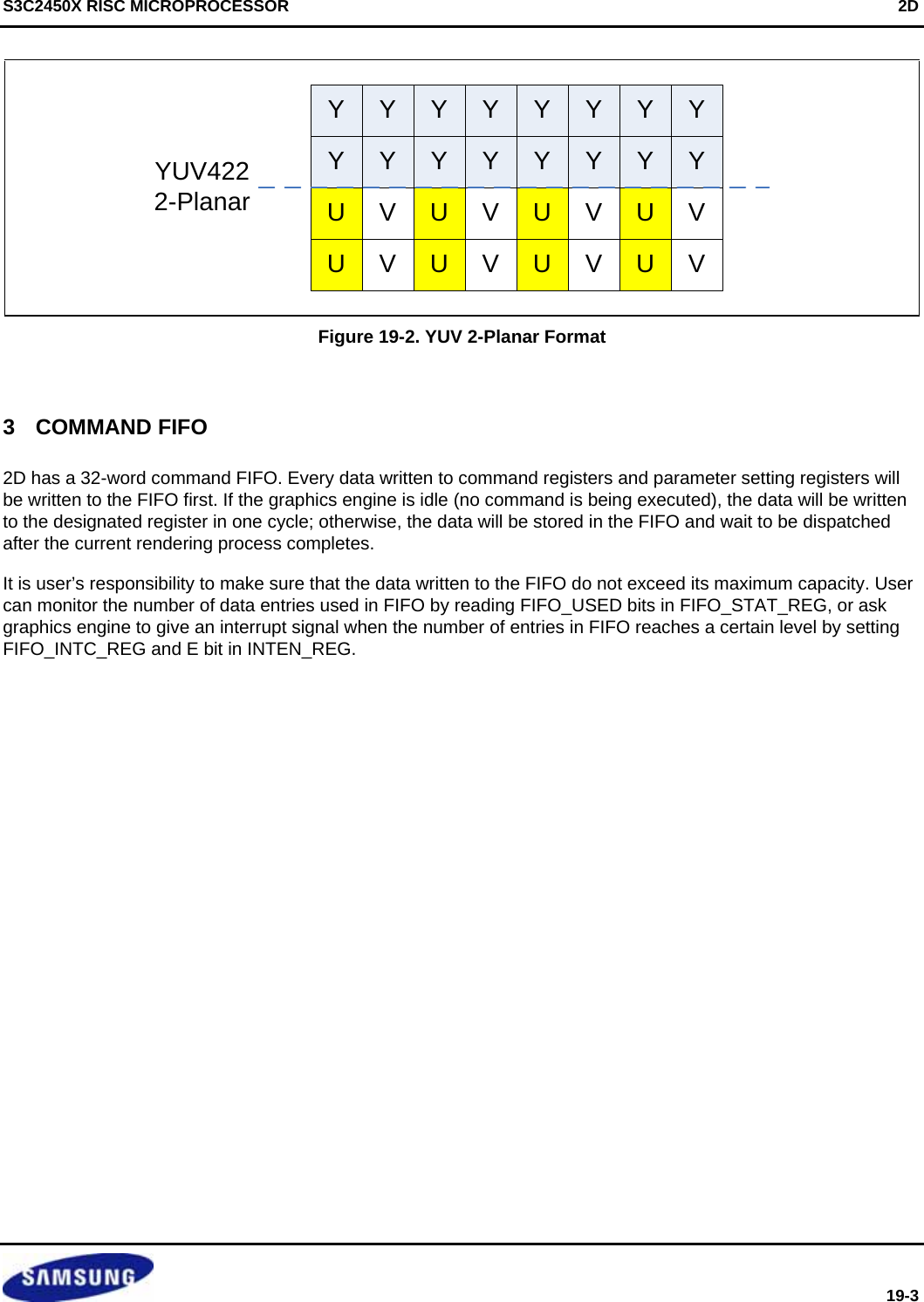
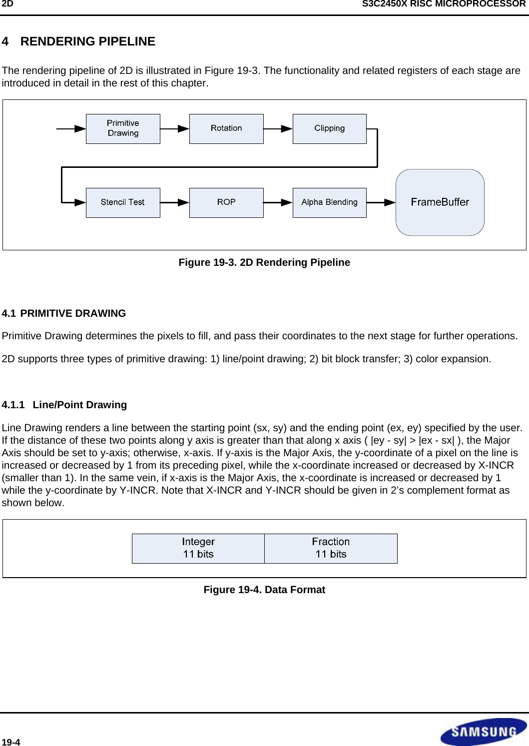
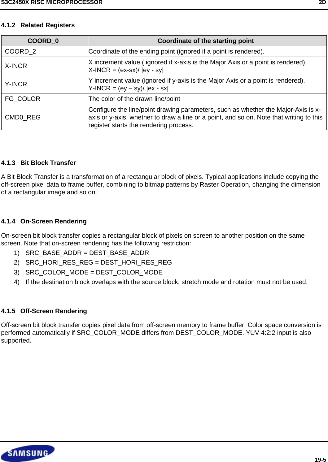

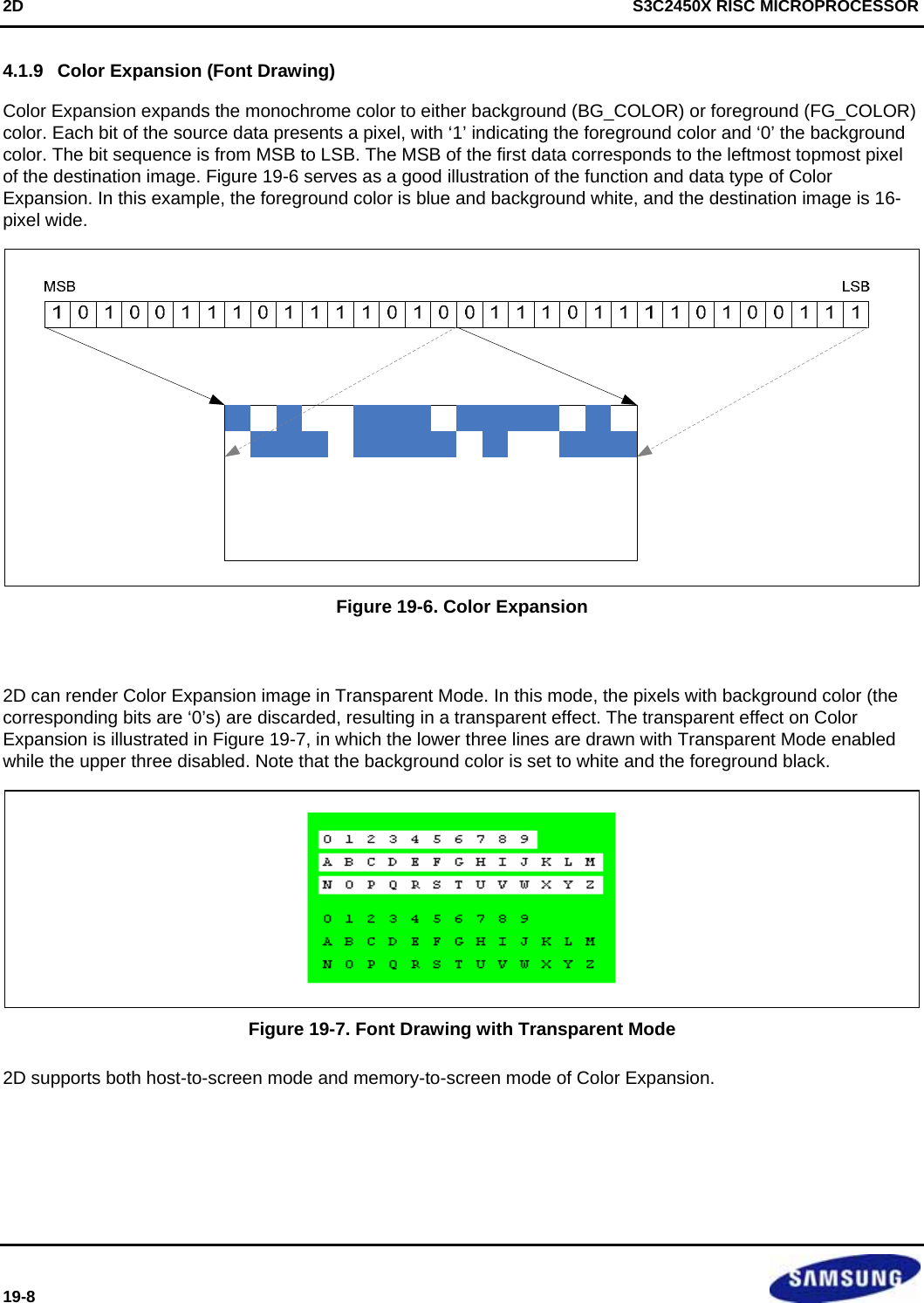
![S3C2450X RISC MICROPROCESSOR 2D 19-11 4.3 CLIPPING Clipping discards the pixels (after rotation) outside the clipping window. The discarded pixels will not go through the rest of rendering pipelines. Note that the clipping windows must reside totally inside the screen. Setting the clipping window the same size with the screen will disable the clipping effect, and a clipping window bigger than the screen size is not allowed. 4.3.1 Related Registers CW_LT_REG Coordinate of the leftmost topmost point of the clipping window CW_RB_REG Coordinate of the rightmost bottommost point of the clipping window 4.4 STENCIL TEST The Stencil Test conditionally discards a pixel based on the outcome of a comparison between the color value of this pixel of the source image and the DR(min)/DR(max) values. If each field (R, G, B, A) of the color value falls in the range of [ DR(min), DR(max)], this pixel is passed to the next stage; otherwise, discarded. User can disable the stencil test on a specific field by clearing the corresponding bits in COLORKEY_CNTL. Note that each field of DR_MIN and DR_MAX is 8-bit wide, regardless of the source color mode setting. 4.4.1 Related Registers COLORKEY_CNTL Stencil Test configurations, such as enable/disable the test and so on. COLORKEY_DR_MIN Set the DR(min) value for each field COLORKEY_DR_MAX Set the DR(max) value for each field 4.5 RASTER OPERATION Raster Operation performs Boolean operations on three operands: source, destination and third operand according to the 8-bit ROP value specified by the user. The truth table of ROP is given in the following table. Source Destination Third Operand ROP Value 0 0 0 Bit0 0 0 1 Bit1 0 1 0 Bit2 0 1 1 Bit3 1 0 0 Bit4 1 0 1 Bit5 1 1 0 Bit6 1 1 1 Bit7](https://usermanual.wiki/Diasonic-Technology-Co/RVM-704M.Users-Manual/User-Guide-1826140-Page-457.png)
![2D S3C2450X RISC MICROPROCESSOR 19-12 The third operand can be pattern or foreground color, configurable by the OS bit in the ROP_REG. Pattern is a user-specified 8x8x16-bpp image; the pattern data should be given in RGB565 format. The following equation is used to calculate the pattern index of pixel (x, y): index = ( ((patternOffsetY + y) & 0x7 )<<3 ) + ((patternOffsetX + x)&0x7), where patternOffsetY and patternOffsetX are the offset value specified in register PATOFF_REG. Here are some examples on how to use the ROP value to perform the operations: 1. Final Data = Source. Only the Source data matter, so ROP Value = “11110000”. 2. Final Data = Destination. Only the Destination data matter, so ROP Value = “11001100”. 3. Final Data = Pattern. Only the Pattern data matter, so ROP Value = “10101010”. 4. Final Data = Source AND Destination. ROP Value = “11110000” & “11001100” = “11000000” 5. Final Data = Source OR Pattern. ROP Value = “11110000” | “10101010” = “11111010”. Note that the Raster Operation only applies on R, G, B fields of the color data; the A field will not be affected. 4.5.1 Related Registers PATTERN_REG[0:31] Pattern data PATOFF_REG Pattern offset X, Y ROP_REG ROP configurations and ROP Value](https://usermanual.wiki/Diasonic-Technology-Co/RVM-704M.Users-Manual/User-Guide-1826140-Page-458.png)
![S3C2450X RISC MICROPROCESSOR 2D 19-13 4.6 ALPHA BLENDING Alpha Blending combines the source color and the destination color in the frame buffer to get the new destination color. The conventional alpha blending equation is: final data = src * alpha + dest * (1.0 − alpha). 2D uses 8-bit integer to represent the alpha value, with 0 indicating 1/256 and 255 indicating 1.0. The equation of converting 8-bit ALPHA value to the actual fractional alpha value is: alpha = (ALPHA+1) / 256. The internal computation of alpha blending and fading is as follows: User-specified alpha value: ALPHA (given by ALPHA_REG, from 0 to 255) [Alpha Blending] data = ( source * (ALPHA+1) + destination * (255-ALPHA) ) >> 8 [Fading] data = (( source * (ALPHA+1) ) >> 8) + fading offset Per-pixel alpha blending: ALPHA (given by the source image, from 0 to 255) [Alpha Blending] data = ( source * (ALPHA+1) + destination * (255-ALPHA) ) >> 8 [Fading] data = ((source * (ALPHA+1) ) >> 8 ) + fading offset 4.6.1 Related Registers ROP_REG Alpha blending configurations: alpha blending disable/enable, per-pixel alpha blending disable/enable, fading disable/enable. ALPHA_REG Alpha value and fading value.](https://usermanual.wiki/Diasonic-Technology-Co/RVM-704M.Users-Manual/User-Guide-1826140-Page-459.png)
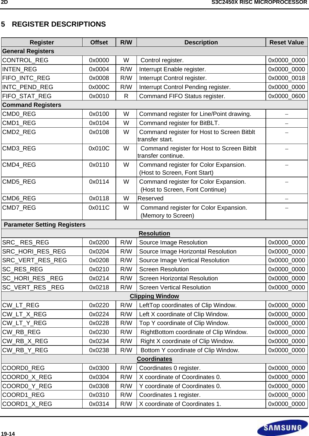
![S3C2450X RISC MICROPROCESSOR 2D 19-15 Register Offset R/W Description Reset ValueCOORD1_Y_REG 0x0318 R/W Y coordinate of Coordinates 1. 0x0000_0000COORD2_REG 0x0320 R/W Coordinates 2 register. 0x0000_0000COORD2_X_REG 0x0324 R/W X coordinate of Coordinates 2. 0x0000_0000COORD2_Y_REG 0x0328 R/W Y coordinate of Coordinates 2. 0x0000_0000COORD3_REG 0x0330 R/W Coordinates 3 register. 0x0000_0000COORD3_X_REG 0x0334 R/W X coordinate of Coordinates 3. 0x0000_0000COORD3_Y_REG 0x0338 R/W Y coordinate of Coordinates 3. 0x0000_0000Rotation ROT_OC_REG 0x0340 R/W Rotation Origin Coordinates. 0x0000_0000ROT_OC_X_REG 0x0344 R/W X coordinate of Rotation Origin Coordinates. 0x0000_0000ROT_OC_Y_REG 0x0348 R/W Y coorindate of Rotation Origin Coordinates. 0x0000_0000ROTATE_REG 0x034C R/W Rotation Mode register. 0x0000_0001X,Y Increment Setting X_INCR_REG 0x0400 R/W X Increment register. 0x0000_0000Y_INCR_REG 0x0404 R/W Y Increment register. 0x0000_0000ROP & Alpha Setting ROP_REG 0x0410 R/W Raster Operation register. 0x0000_0000ALPHA_REG 0x0420 R/W Alpha value, Fading offset. 0x0000_0000Color FG_COLOR_REG 0x0500 R/W Foreground Color / Alpha register. 0x0000_0000BG_COLOR_REG 0x0504 R/W Background Color register 0x0000_0000BS_COLOR_REG 0x0508 R/W Blue Screen Color register 0x0000_0000SRC_COLOR_MODE_REG 0x0510 R/W Src Image Color Mode register. 0x0000_0000DEST_COLOR_MODE_REG 0x0514 R/W Dest Image Color Mode register 0x0000_0000Pattern PATTERN_REG[0:31] 0x0600 ~0x067C R/W Pattern memory. 0x0000_0000PATOFF_REG 0x0700 R/W Pattern Offset XY register. 0x0000_0000PATOFF_X_REG 0x0704 R/W Pattern Offset X register. 0x0000_0000PATOFF_Y_REG 0x0708 R/W Pattern Offset Y register. 0x0000_0000Stencil Test STENCIL_CNTL_REG 0x0720 R/W Stencil control register 0x0000_0000STENCIL_DR_MIN_REG 0x0724 W Stencil decision reference MIN register 0x0000_0000STENCIL_DR_MAX_REG 0x0728 W Stencil decision reference MAX register 0xFFFF_FFFFImage Base Address SRC_BASE_ADDR_REG 0x0730 R/W Source Image Base Address register 0x0000_0000DEST_BASE_ADDR_REG 0x0734 R/W Dest Image Base Address register (in most cases, frame buffer address) 0x0000_0000](https://usermanual.wiki/Diasonic-Technology-Co/RVM-704M.Users-Manual/User-Guide-1826140-Page-461.png)
![2D S3C2450X RISC MICROPROCESSOR 19-16 5.1 GENERAL REGISTERS 5.1.1 Control Register (CONTROL_REG) Register Address R/W Description Reset ValueCONTROL_REG 0x4D408000 W Control register 0x0 Field Bit Description Initial StateReserved [31:1] − 0x0 R [0] Software Reset Write to this bit results in a one-cycle reset signal to FIMG2D graphics engine. Every command register and parameter setting register will be assigned the “Reset Value”, and the command FIFO will be cleared. 0x0 5.1.2 Interrupt Enable Register (INTEN_REG) Register Address R/W Description Reset ValueINTEN_REG 0x4D408004 R/W Interrupt Enable register 0x0 Field Bit Description Initial StateReserved [31:11] − 0x0 CCF [10] Current Command Finished interrupt enable. If this bit is set, when the graphics engine finishes the execution of current command, an interrupt occurs, and the INTP_CMD_FIN flag in INTC_PEND_REG will be set. ACF [9] All Commands Finished interrupt enable. If this bit is set, when the graphics engine finishes the execution of all commands in the command FIFO, an interrupt occurs, and the INTP_ALL_FIN flag in INTC_PEND_REG will be set. 0x0 FIFO_FULL [8] Command FIFO Full interrupt enable. If this bit is set, when command FIFO is full (32 entries), an interrupt occurs, and the INTP_FULL flag in the interrupt pending register (INTC_PEND_REG) will be set. 0x0 Reserved [7:1] − 0x0 FIFO_INT_E [0] If this bit is set, when the number of entries occupied in command FIFO is greater or equal to FIFO_INT_LEVEL (in FIFO_INTC_REG), an interrupt occurs, and the INTP_FIFO_LEVEL flag in the interrupt pending register (INTC_PEND_REG) will be set. 0x0](https://usermanual.wiki/Diasonic-Technology-Co/RVM-704M.Users-Manual/User-Guide-1826140-Page-462.png)
![S3C2450X RISC MICROPROCESSOR 2D 19-17 5.1.3 FIFO Interrupt Control Register (FIFO_INTC_REG) Register Address R/W Description Reset ValueFIFO_INTC_REG 0x4D408008 R/W FIFO Interrupt Control 0x18 Field Bit Description Initial State Reserved [31:6] − 0x0 FIFO_INT_LEVEL [5:0] If FIFO_INT_E (in INTEN_REG) is set, when FIFO_USED (in FIFO_STAT_REG) is greater or equal to FIFO_INT_LEVEL, an interrupt occurs. 0x18 5.1.4 Interrupt Pending Register (INTC_PEND_REG) Register Address R/W Description Reset Value INTC_PEND_REG 0x4D40800C R/W Interrupt Pending Register 0x0 Field Bit Description Initial StateReserved [31] Should be set ‘1’ − Reserved [30:11] Reserved − INTP_CMD_FIN [10] Current Command Finished interrupt flag. Writing ‘1’ to this bit clears this flag. − INTP_ALL_FIN [9] All Commands Finished interrupt flag. Writing ‘1’ to this bit clears this flag. − INTP_FULL [8] Command FIFO Full interrupt flag. Writing ‘1’ to this bit clears this flag. − Reserved [7:1] − − INTP_FIFO_LEVEL [0] FIFO_USED reaches FIFO_INT_LEVEL interrupt flag. Writing ‘1’ to this bit clears this flag. −](https://usermanual.wiki/Diasonic-Technology-Co/RVM-704M.Users-Manual/User-Guide-1826140-Page-463.png)
![2D S3C2450X RISC MICROPROCESSOR 19-18 5.1.5 FIFO Statue Register (FIFO_STAT_REG) Register Address R/W Description Reset ValueFIFO_STAT_REG 0x4D408010 R FIFO Status Register 0x600 Field Bit Description Initial StateReserved [31:11] − − CMD_FIN [10] 1 = The graphics engine finishes the execution of current command. 0 = In the middle of rendering process. 0x1 ALL_FIN [9] 1 = Graphics engine is in idle state. The graphics engine finishes the execution of all commands in the command FIFO. Note that ALL_FIN = CMD_FIN && (FIFO_USED==0). 0 = In the middle of rendering process, or FIFO_USED is greater than 0. 0x1 FIFO_OVERFLOW [8] 1 = Command FIFO is full, no more commands can be handled 0 = Command FIFO is not full. 0x0 Reserved [7] − − FIFO_USED [6:1] The number of entries occupied in command FIFO. 0x0 FIFO_LEVEL_INT [0] 1 = FIFO_USED is greater or equal to FIFO_INT_LEVEL 0 = FIFO_USED is smaller than FIFO_INT_LEVEL 0x0](https://usermanual.wiki/Diasonic-Technology-Co/RVM-704M.Users-Manual/User-Guide-1826140-Page-464.png)
![S3C2450X RISC MICROPROCESSOR 2D 19-19 5.2 COMMAND REGISTERS 5.2.1 LINE Drawing Register (CMD0_REG) Register Address R/W Description Reset ValueCMD0_REG 0x4D408100 W Line Drawing Register 0x0 Field Bit Description Initial StateReserved [31:10] − − D [9] 0 = Draw Last Point 1 = Do-not-Draw Last Point. − M [8] 0 = Major axis is Y. 1 = Major axis is X. − Reserved [7:2] − − L [1] 0 = Nothing. 1 = Line Drawing. − P [0] 0 = Nothing. 1 = Point Drawing. − 5.2.2 BitBLT Register (CMD1_REG) Register Address R/W Description Reset ValueCMD1_REG 0x4D408104 W BitBLT Register 0x0 Field Bit Description Initial StateReserved [31:2] − − S [1] 0 = Nothing 1 = Stretch BitBLT − N [0] 0 = Nothing 1 = Normal BitBLT − 5.2.3 HOST Screen Start BitBLT Register (CMD2_REG) Register Address R/W Description Reset ValueCMD2_REG 0x4D408108 W Host to Screen Start BitBLT Register 0x0 Field Bit Description Initial StateData [31:0] BitBLT data (Start) Note that the data written to this register represents only one pixel, regardless of the source color mode. If the source color mode is 16-bpp (e.g., RGB565), the upper 16 bits of the data are ignored. −](https://usermanual.wiki/Diasonic-Technology-Co/RVM-704M.Users-Manual/User-Guide-1826140-Page-465.png)
![2D S3C2450X RISC MICROPROCESSOR 19-20 5.2.4 Host to Screen Continue BitBLT Register (CMD3_REG) Register Address R/W Description Reset ValueCMD3_REG 0x4D40810C W Host to Screen Continue BitBLT Register 0x0 Field Bit Description Initial StateData [31:0] BitBLT data (Continue) Note that the data written to this register represents only one pixel, regardless of the source color mode. If the source color mode is 16-bpp (e.g., RGB565), the upper 16 bits of the data are ignored. − 5.2.5 Host to Screen Start Color Expansion Register (CMD4_REG) Register Address R/W Description Reset ValueCMD4_REG 0x4D408110 W Host to Screen Start Color Expansion Register 0x0 Field Bit Description Initial StateData [31:0] Color Expansion Data (Start) − 5.2.6 Host to Screen Continue Color Expansion Register (CMD5_REG) Register Address R/W Description Reset ValueCMD5_REG 0x4D408114 W Host to Screen Continue Color Expansion Register 0x0 Field Bit Description Initial StateData [31:0] Color Expansion Data (Continue) − 5.2.7 Memory to Screen Color Expansion Register (CMD7_REG) Register Address R/W Description Reset ValueCMD7_REG 0x4D40811C W Memory to Screen Color Expansion Register 0x0 Field Bit Description Initial StateMemory Address [31:0] Bitmap data base address (used in memory-to-screen mode, should be word-aligned). −](https://usermanual.wiki/Diasonic-Technology-Co/RVM-704M.Users-Manual/User-Guide-1826140-Page-466.png)
![S3C2450X RISC MICROPROCESSOR 2D 19-21 5.3 PARAMETER SETTING REGISTERS Resolution 5.3.1 Source Image Resolution Register (SRC_RES_REG) Register Address R/W Description Reset ValueSRC_RES_REG 0x4D408200 R/W Source Image Resolution Register 0x0 Field Bit Description Initial StateReserved [31:27] 0x0 VertRes [26:16] Vertical resolution of source image. Range: 1 ~ 2040 0x0 Reserved [15:11] 0x0 HoriRes [10:0] Horizontal resolution of source image. Range: 1 ~ 2040. Note that in YUV mode, HoriRes must be an even number. 0x0 5.3.2 Source Image Horizontal Resolution Register (SRC_HORI_RES_REG) Register Address R/W Description Reset ValueSRC_HORI_RES_REG 0x4D408204 R/W Source Image Horizontal Resolution Register 0x0 Field Bit Description Initial StateReserved [31:1] − 0x0 HoriRes [10:0] Horizontal resolution of source image. Range: 1 ~ 2040. Note that in YUV mode, HoriRes must be an even number. 0x0 5.3.3 Source Image Horizontal Resolution Register (SRC_HORI_RES_REG) Register Address R/W Description Reset ValueSRC_HORI_RES_REG 0x4D408204 R/W Source Image Horizontal Resolution Register 0x0 Field Bit Description Initial StateReserved [31:1] − 0x0 VertRes [10:0] Vertical resolution of source image. Range: 1 ~ 2040 0x0](https://usermanual.wiki/Diasonic-Technology-Co/RVM-704M.Users-Manual/User-Guide-1826140-Page-467.png)
![2D S3C2450X RISC MICROPROCESSOR 19-22 5.3.4 Screen Resolution Register (SC_RES_REG) Register Address R/W Description Reset ValueSC_RES_REG 0x4D408210 R/W Screen Resolution Register 0x0 Field Bit Description Initial StateReserved [31:27] − 0x0 VertRes [26:16] Vertical resolution of the screen. Range: 1 ~ 2040 0x0 Reserved [15:11] − 0x0 HoriRes [10:0] Horizontal resolution of the screen. Range: 1 ~ 2040 0x0 5.3.5 Screen Horizontal Resolution Register (SC_HORI_RES_REG) Register Address R/W Description Reset ValueSC_HORI_RES_ REG 0x4D408214 R/W Screen Horizontal Resolution Register 0x0 Field Bit Description Initial StateReserved [31:11] − 0x0 HoriRes [10:0] Horizontal resolution of the screen. Range: 1 ~ 2040 0x0 5.3.6 Screen Vertical Resolution Register (SC_VERI_RES_REG) Register Address R/W Description Reset ValueSC_VERI_RES_ REG 0x4D408218 R/W Screen Vertical Resolution Register 0x0 Field Bit Description Initial StateReserved [31:1] − 0x0 VeriRes [10:0] Vertical resolution of the screen. Range: 1 ~ 2040 0x0](https://usermanual.wiki/Diasonic-Technology-Co/RVM-704M.Users-Manual/User-Guide-1826140-Page-468.png)
![S3C2450X RISC MICROPROCESSOR 2D 19-23 Clipping Window 5.3.7 LeftTop Clipping Window Register (CW_LT_REG) Register Address R/W Description Reset ValueCW_LT_REG 0x4D408220 R/W LeftTop Clipping Window Register 0x0 Field Bit Description Initial StateReserved [31:27] − 0x0 TopCW_Y [26:16] Top Y Clipping Window Requirement: TopCW_Y < BottomCW_Y 0x0 Reserved [15:11] − 0x0 LeftCW_X [10:0] Left X Coordinate of Clipping Window. Requirement: LeftCW_X < RightCW_X 0x0 5.3.8 Left X Clipping Window Register (CW_LT_X_REG) Register Address R/W Description Reset ValueCW_LT_X_REG 0x4D408224 R/W Left X Clipping Window Register 0x0 Field Bit Description Initial StateReserved [31:11] − 0x0 LeftCW_X [10:0] Left X Clipping Window Requirement: LeftCW_X < RightCW_X 0x0 5.3.9 Top Y Clipping Window Register (CW_LT_Y_REG) Register Address R/W Description Reset ValueCW_LT_Y_REG 0x4D408228 R/W Top Y Clipping Window Register 0x0 Field Bit Description Initial StateReserved [31:11] − 0x0 TopCW_Y [10:0] Top Y Clipping Window Requirement: TopCW_Y < BottomCW_Y 0x0](https://usermanual.wiki/Diasonic-Technology-Co/RVM-704M.Users-Manual/User-Guide-1826140-Page-469.png)
![2D S3C2450X RISC MICROPROCESSOR 19-24 5.3.10 RightBottom Clipping Window Register (CW_RB_REG) Register Address R/W Description Reset ValueCW_RB_REG 0x4D408230 R/W RightBottom Clipping Window Register 0x0 Field Bit Description Initial StateReserved [31:27] − 0x0 BottomCW_Y [26:16] Bottom Y Clipping Window Requirement: BottomCW_Y < VeriRes (SC_VERI_RES_REG) 0x0 Reserved [15:11] − 0x0 RightCW_X [10:0] Right X Clipping Window Requirement: RightCW_X < HoriRes (SC_HORI_RES_REG) 0x0 5.3.11 Right X Clipping Window Register (CW_RB_X_REG) Register Address R/W Description Reset ValueCW_RB_X_REG 0x4D408234 R/W Right X Clipping Window Register 0x0 Field Bit Description Initial StateReserved [31:11] − 0x0 RightCW_X [10:0] Right X Clipping Window Requirement: RightCW_X < HoriRes (SC_HORI_RES_REG) 0x0 5.3.12 Bottom Y Clipping Window Register (CW_RB_Y_REG) Register Address R/W Description Reset ValueCW_RB_Y_REG 0x4D408238 R/W Bottom Y Clipping Window Register 0x0 Field Bit Description Initial StateReserved [31:11] − 0x0 BottomCW_Y [10:0] Bottom Y Clipping Window Requirement: BottomCW_Y < VeriRes (SC_VERI_RES_REG) 0x0](https://usermanual.wiki/Diasonic-Technology-Co/RVM-704M.Users-Manual/User-Guide-1826140-Page-470.png)
![S3C2450X RISC MICROPROCESSOR 2D 19-25 Coordinates 5.3.13 COORDINATE_0 Register (COORD0_REG) Register Address R/W Description Reset ValueCOORD0_REG 0x4D408300 R/W Coordinate_0 Register 0x0 Field Bit Description Initial StateReserved [31:27] − 0x0 Y [26:16] Coordinate_0 Y Range: 0 ~ 2039 0x0 Reserved [15:11] − 0x0 X [10:0] Coordinate_0 X Range: 0 ~ 2039 0x0 5.3.14 COORDINATE_0 X Register (COORD0_X_REG) Register Address R/W Description Reset ValueCOORD0_X_REG 0x4D408304 R/W Coordinate_0 X Register 0x0 Field Bit Description Initial StateReserved [31:11] − 0x0 COORD0_X [10:0] Coordinate_0 X Range: 0 ~ 2039 0x0 5.3.15 COORDINATE_0 Y Register (COORD0_Y_REG) Register Address R/W Description Reset ValueCOORD0_Y_REG 0x4D408308 R/W Coordinate_0 Y Register 0x0 Field Bit Description Initial StateReserved [31:11] − 0x0 COORD0_Y [10:0] Coordinate_0 Y Range: 0 ~ 2039 0x0](https://usermanual.wiki/Diasonic-Technology-Co/RVM-704M.Users-Manual/User-Guide-1826140-Page-471.png)
![2D S3C2450X RISC MICROPROCESSOR 19-26 5.3.16 COORDINATE_1 Register (COORD1_REG) Register Address R/W Description Reset ValueCOORD1_REG 0x4D408310 R/W Coordinate_1 Register 0x0 Field Bit Description Initial StateReserved [31:27] − 0x0 Y [26:16] Coordinate_1 Y Range: 0 ~ 2039 0x0 Reserved [15:11] − 0x0 X [10:0] Coordinate_1 X Range: 0 ~ 2039 0x0 5.3.17 COORDINATE_1 X Register (COORD1_X_REG) Register Address R/W Description Reset ValueCOORD1_X_REG 0x4D408314 R/W Coordinate_1 X Register 0x0 Field Bit Description Initial StateReserved [31:11] − 0x0 COORD1_X [10:0] Coordinate_1 X Range: 0 ~ 2039 0x0 5.3.18 COORDINATE_1 Y Register (COORD1_Y_REG) Register Address R/W Description Reset ValueCOORD1_Y_REG 0x4D408318 R/W Coordinate_1 Y Register 0x0 Field Bit Description Initial StateReserved [31:11] − 0x0 COORD1_Y [10:0] Coordinate_1 Y Range: 0 ~ 2039 0x0](https://usermanual.wiki/Diasonic-Technology-Co/RVM-704M.Users-Manual/User-Guide-1826140-Page-472.png)
![S3C2450X RISC MICROPROCESSOR 2D 19-27 5.3.19 COORDINATE_2 Register (COORD2 _REG) Register Address R/W Description Reset ValueCOORD2_REG 0x4D408320 R/W Coordinate_2 Register 0x0 Field Bit Description Initial StateReserved [31:27] − 0x0 Y [26:16] Coordinate_2 Y Range: 0 ~ 2039 0x0 Reserved [15:11] − 0x0 X [10:0] Coordinate_2 X Range: 0 ~ 2039 0x0 5.3.20 COORDINATE_2 X Register (COORD2_X_REG) Register Address R/W Description Reset ValueCOORD2_ X_REG 0x4D408324 R/W Coordinate_2 X Register 0x0 Field Bit Description Initial StateReserved [31:11] − 0x0 COORD2_X [10:0] Coordinate_2 X Range: 0 ~ 2039 0x0 5.3.21 COORDINATE_2 Y Register (COORD2_Y_REG) Register Address R/W Description Reset ValueCOORD2_ Y_REG 0x4D408328 R/W Coordinate_2 Y Register 0x0 Field Bit Description Initial StateReserved [31:11] − 0x0 COORD2_Y [10:0] Coordinate_2 Y Range: 0 ~ 2039 0x0](https://usermanual.wiki/Diasonic-Technology-Co/RVM-704M.Users-Manual/User-Guide-1826140-Page-473.png)
![2D S3C2450X RISC MICROPROCESSOR 19-28 5.3.22 COORDINATE_3 REGISTER (COORD3 _REG) Register Address R/W Description Reset ValueCOORD3_REG 0x4D408330 R/W Coordinate_3 Register 0x0 Field Bit Description Initial StateReserved [31:27] − 0x0 Y [26:16] Coordinate_3 Y Range: 0 ~ 2039 0x0 Reserved [15:11] − 0x0 X [10:0] Coordinate_3 X Range: 0 ~ 2039 0x0 5.3.23 COORDINATE_3 X Register (COORD3_X_REG) Register Address R/W Description Reset ValueCOORD3_ X_REG 0x4D408334 R/W Coordinate_3 X Register 0x0 Field Bit Description Initial StateReserved [31:11] − 0x0 COORD3_X [10:0] Coordinate_3 X Range: 0 ~ 2039 0x0 5.3.24 COORDINATE_3 Y Register (COORD3_Y_REG) Register Address R/W Description Reset ValueCOORD3_ Y_REG 0x4D408338 R/W Coordinate_3 Y Register 0x0 Field Bit Description Initial StateReserved [31:11] − 0x0 COORD3_Y [10:0] Coordinate_3 Y Range: 0 ~ 2039 0x0](https://usermanual.wiki/Diasonic-Technology-Co/RVM-704M.Users-Manual/User-Guide-1826140-Page-474.png)
![S3C2450X RISC MICROPROCESSOR 2D 19-29 Rotation 5.3.25 Rotation Origin Coordinate Register (ROT_OC_REG) Register Address R/W Description Reset ValueROT_OC_REG 0x4D408340 R/W Rotation Origin Coordinate Register 0x0 Field Bit Description Initial StateReserved [31:27] − 0x0 Y [26:16] X coordinate of the reference point of rotation Range: 0 ~ 2039 0x0 Reserved [15:11] − 0x0 X [10:0] Y coordinate of the reference point of rotation Range 0 ~ 2039 0x0 5.3.26 Rotation Origin Coordinate X Register (ROT_OC_X_REG) Register Address R/W Description Reset ValueROT_OC_X 0x4D408344 R/W Rotation Origin Coordinate X Register 0x0 Field Bit Description Initial StateReserved [31:11] − 0x0 ROT_OC_X [10:0] X coordinate of the reference point of rotation Range: 0 ~ 2039 0x0 5.3.27 Rotation Origin Coordinate Y Register (ROT_OC_Y_REG) Register Address R/W Description Reset ValueROT_OC_Y 0x4D408348 R/W Rotation Origin Coordinate Y Register 0x0 Field Bit Description Initial StateReserved [31:1] − 0x0 ROT_OC_Y [10:0] Y coordinate of the reference point of rotation Range 0 ~ 2039 0x0](https://usermanual.wiki/Diasonic-Technology-Co/RVM-704M.Users-Manual/User-Guide-1826140-Page-475.png)
![2D S3C2450X RISC MICROPROCESSOR 19-30 5.3.28 Rotation Register (ROTATE_REG) Register Address R/W Description Reset ValueROTATE_REG 0x4D40834C R/W Rotation Register 0x0 Field Bit Description Initial StateReserved [31:6] 0x0 FY [5] Y-flip 0x0 FX [4] X-flip 0x0 R3 [3] 270° Rotation 0x0 R2 [2] 180° Rotation 0x0 R1 [1] 90° Rotation 0x0 R0 [0] 0° Rotation 0x1 * If the two or more of Rn are set to 1 at the same time, drawing engine operates unpredictably.](https://usermanual.wiki/Diasonic-Technology-Co/RVM-704M.Users-Manual/User-Guide-1826140-Page-476.png)
![S3C2450X RISC MICROPROCESSOR 2D 19-31 X,Y Increment Setting 5.3.29 X Increment Register (X_INCR_REG) Register Address R/W Description Reset ValueX_INCR_REG 0x4D408400 R/W X Increment Register 0x0 Field Bit Description Initial StateReserved [31:22] − 0x0 X_INCR [21:0] X increment value (2’s complement, 11-digit fraction) 0x0 5.3.30 Y Increment Register (Y_INCR_REG) Register Address R/W Description Reset ValueY_INCR_REG 0x4D408404 R/W Y Increment Register 0x0 Field Bit Description Initial StateReserved [31:22] − 0x0 Y_INCR [21:0] Y increment value (2’s complement, 11-digit fraction) 0x0](https://usermanual.wiki/Diasonic-Technology-Co/RVM-704M.Users-Manual/User-Guide-1826140-Page-477.png)
![2D S3C2450X RISC MICROPROCESSOR 19-32 ROP & Alpha Setting 5.3.31 Raster Operation Register (ROP_REG) Register Address R/W Description Reset ValueROP_REG 0x4D408410 R/W Raster Operation Register 0x0 Field Bit Description Initial StateReserved [31:14] − 0x0 OS [13] Third Operand Select : 1’b0 = Pattern 1’b1 = Foreground Color 0x0 ABM [12:10] Alpha Mode : 3’b000 = No Alpha Blending 3’b001 = Perpixel Alpha Blending with Source Bitmap 3’b010 = Alpha Blending with Alpha Register 3’b100 = Fading Others = Reserved Note that Perpixel Alpha Blending can only be applied on bit block transfer. 0x0 T [9] 0 = Opaque Mode 1 = Transparent Mode 0x0 Reserved [8] Reserved 0x0 ROP Value [7:0] Raster Operation Value 0x0 5.3.32 Alpha Register (ALPHA_REG) Register Address R/W Description Reset ValueALPHA_REG 0x4D408420 R/W Alpha Register 0x0 Field Bit Description Initial StateReserved [31:16] − 0x0 Fading [15:8] Fading Offset Value 0x0 Alpha [7:0] Alpha Value 0x0](https://usermanual.wiki/Diasonic-Technology-Co/RVM-704M.Users-Manual/User-Guide-1826140-Page-478.png)
![S3C2450X RISC MICROPROCESSOR 2D 19-33 Color 5.3.33 Foreground Color Register (FG_COLOR_REG) Register Address R/W Description Reset ValueFG_COLOR_REG 0x4D408500 R/W Foreground Color Register 0x0 Field Bit Description Initial StateForegroundColor [31:0] Foreground Color Value. The alpha field of the foreground color will be discarded. 0x0 5.3.34 Backround Color Register (BG_COLOR_REG) Register Address R/W Description Reset ValueBG_COLOR_REG 0x4D408504 R/W Background Color Register 0x0 Field Bit Description Initial StateBackgroundColor [31:0] Background Color Value. The alpha field of the background color will be discarded. 0x0 5.3.35 BlueScreen Color Register (BS_COLOR_REG) Register Address R/W Description Reset ValueBS_COLOR_REG 0x4D408508 R/W BlueScreen Color Register 0x0 Field Bit Description Initial StateBlueScreenColor [31:0] BlueScreen Color Value. The alpha field of the blue screen color will be discarded. 0x0](https://usermanual.wiki/Diasonic-Technology-Co/RVM-704M.Users-Manual/User-Guide-1826140-Page-479.png)
![2D S3C2450X RISC MICROPROCESSOR 19-34 5.3.36 Source Image Color Mode Register (SRC_COLOR_MODE_REG) Register Address R/W Description Reset ValueSRC_COLOR_ MODE_REG 0x4D408510 R/W Source Image Color Mode Register 0x0 Field Bit Description Initial StateReserved [31:5] − 0x0 Narrow [4] 1 = YUV narrow range (Y:16-235, UV: 16-240) 0 = YUV wide range (YUV: 0-255) 0x0 YUV [3] 1 = YUV mode 0 = RGB mode This bit should be set to 0 in point/line drawing mode and color expansion mode. 0x0 Color Setting [2:0] 3’b000 = RGB_565 3’b001 = RGBA_5551 3’b010 = ARGB_1555 3’b011 = RGBA_8888 3’b100 = ARGB_8888 3’b101 = XRGB_8888 3’b110 = RGBX_8888 The Color Setting is ignored if YUV mode is selected 0x0 5.3.37 Destination Image Color Mode Register (DEST_COLOR_MODE_REG) Register Address R/W Description Reset ValueDEST_COLOR_ MODE_REG 0x4D408514 R/W Destination Image Color Mode Register 0x0 Field Bit Description Initial StateReserved [31:4] − 0x0 Color Setting [2:0] 3’b000 = RGB_565 3’b001 = RGBA_5551 3’b010 = ARGB_1555 3’b011 = RGBA_8888 3’b100 = ARGB_8888 3’b101 = XRGB_8888 3’b110 = RGBX_8888 0x0](https://usermanual.wiki/Diasonic-Technology-Co/RVM-704M.Users-Manual/User-Guide-1826140-Page-480.png)
![S3C2450X RISC MICROPROCESSOR 2D 19-35 Pattern 5.3.38 Pattern Register (PAT_REG) Register Address R/W Description Reset ValuePAT_REG 0x4D408600 ~ 67C R/W Pattern Register 0x0 Field Bit Description Initial StatePAT_REG [31:0] Pattern Register 0x0 5.3.39 Pattern Offset Register (PATOFF_REG) Register Address R/W Description Reset ValuePATOFF_REG 0x4D408700 R/W Pattern Offset Register 0x0 Field Bit Description Initial StateReserved [31:19] − 0x0 POffsetY [18:16] Pattern OffsetY Value 0x0 Reserved [15:3] − 0x0 POffsetX [2:0] Pattern OffsetX Value 0x0 5.3.40 Pattern Offset X Register (PATOFF_X_REG) Register Address R/W Description Reset ValuePATOFF_X_REG 0x4D408704 R/W Pattern Offset X Register 0x0 Field Bit Description Initial StateReserved [31:3] − 0x0 POffsetX [2:0] Pattern OffsetX Value 0x0 5.3.41 Pattern Offset Y Register (PATOFF_Y_REG) Register Address R/W Description Reset ValuePATOFF_Y_REG 0x4D408708 R/W Pattern Offset Y Register 0x0 Field Bit Description Initial StateReserved [31:3] − 0x0 POffsetY [2:0] Pattern OffsetY Value 0x0](https://usermanual.wiki/Diasonic-Technology-Co/RVM-704M.Users-Manual/User-Guide-1826140-Page-481.png)
![2D S3C2450X RISC MICROPROCESSOR 19-36 Stencil Test 5.3.42 Colorkey Control Register (COLORKEY_CTRL_REG) Register Address R/W Description Reset ValueCOLORKEY_CTRL _REG 0x4D408720 R/W Colorkey Control Register 0x0 Field Bit Description Initial StateReserved [31:5] − 0x0 StencilInverse [4] 0 = Normal stencil test 1 = Inversed stencil test This bit should be set to 0 if the stencil test of every color field is disabled. 0x0 StencilOnR [3] 0 = Stencil Test Off for R value 1 = Stencil Test On for R value 0x0 StencilOnG [2] 0 = Stencil Test Off for G value 1 = Stencil Test On for G value 0x0 StencilOnB [1] 0 = Stencil Test Off for B value 1 = Stencil Test On for B value 0x0 StencilOnA [0] 0 = Stencil Test Off for A value 1 = Stencil Test On for A value 0x0 5.3.43 Colorkey Decision Reference Minimum Register (COLORKEY_DR_MIN_REG) Register Address R/W Description Reset ValueCOLORKEY_DR_MIN_REG 0x4D408724 R/W Colorkey Decision Reference Minimum Register 0x0 Field Bit Description Initial StateA_DR(min) [31:24] Alpha DR MIN value 0x0 R_DR(min) [23:16] RED DR MIN value 0x0 G_DR(min) [15:8] GREEN DR MIN value 0x0 B_DR(min) [7:0] BLUE DR MIN value 0x0](https://usermanual.wiki/Diasonic-Technology-Co/RVM-704M.Users-Manual/User-Guide-1826140-Page-482.png)
![S3C2450X RISC MICROPROCESSOR 2D 19-37 5.3.44 COLORKEY DECISION REFERENCE MAXIMUM REGISTER (COLORKEY_DR_MAX_REG) Register Address R/W Description Reset Value COLORKEY_DR_MAX_REG 0x4D408728 R/W Colorkey Decision Reference Maximum Register 0xFFFF_FFFF Field Bit Description Initial State A_DR(max) [31:24] Alpha DR MAX value 0xF R_DR(max) [23:16] RED DR MAX value 0xF G_DR(max) [15:8] GREEN DR MAX value 0xF B_DR(max) [7:0] BLUE DR MAX value 0xF Image Base Address 5.3.45 Source Image Base Address Register (SRC_BASE_ADDR_REG) Register Address R/W Description Reset Value SRC_BASE_ ADDR_REG 0x4D408730 R/W Source Image Base Address Register 0x0 Field Bit Description Initial State ADDR [31:0] Base address of the source image 0x0 5.3.46 Destination Image Base Address Register (DEST_BASE_ADDR_REG) Register Address R/W Description Reset Value DEST_BASE_ ADDR_REG 0x4D408734 R/W Destination Image Base Address Register 0x0 Field Bit Description Initial State ADDR [31:0] Base address of the destination image (in most cases, it is also the frame buffer base address). 0x0](https://usermanual.wiki/Diasonic-Technology-Co/RVM-704M.Users-Manual/User-Guide-1826140-Page-483.png)

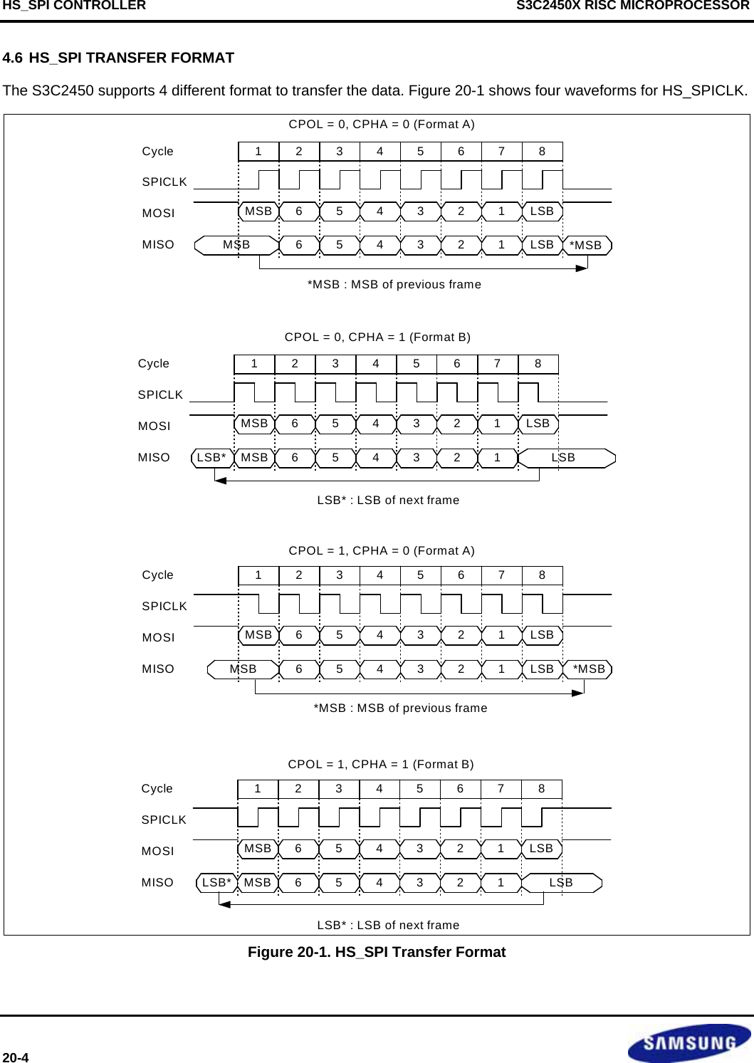
![HS_SPI CONTROLLER S3C2450X RISC MICROPROCESSOR 20-6 5.2 SPECIAL FUNCTION REGISTER Register Address R/W Description Reset Value CH_CFG(Ch0) 0x52000000 R/W HS_SPI configuration register 0x0000_0040CH_CFG(Ch1) 0x59000000 R/W HS_SPI configuration register 0x0000_0040 CH_CFG Bit Description Initial State Reserved [31:7] − 26’b0 High_speed_en [6] 0 = Low speed operation support at slave mode. 1 = High speed operation support at slave mode. 1’b1 SW_RST [5] Software reset 0 = Inactive 1 = Active 1’b0 SLAVE [4] Whether HS_SPI Channel is Master or Slave. 0 = Master 1 = Slave 1’b0 CPOL [3] Determine an active high or active low clock 0 = Active high 1 = Active low 1’b0 CPHA [2] Select one of the two fundamentally different transfer format 0 = Format A 1 = Format B 1’b0 RxChOn [1] HS_SPI Rx Channel On 0 = Channel Off 1 = Channel On 1’b0 TxChOn [0] HS_SPI Tx Channel On 0 = Channel Off 1 = Channel On 1’b0](https://usermanual.wiki/Diasonic-Technology-Co/RVM-704M.Users-Manual/User-Guide-1826140-Page-490.png)
![S3C2450X RISC MICROPROCESSOR HS_SPI CONTROLLER 20-7 Register Address R/W Description Reset ValueClk_CFG(Ch0) 0x52000004 R/W Clock configuration register 0x0 Clk_CFG(Ch1) 0x59000004 R/W Clock configuration register 0x0 Clk_CFG Bit Description Initial State ClkSel [10:9] Clock source selection to generate HS_SPI clock-out 00 = PCLK 01 = USBCLK 10 = Epll clock 11 = Reserved * For using USBCLK source, The USB_SIG_MASK at system controller should be set to on. * Epll clock is from System Controller and has 4 sources: MOUTEPLL, DOUTMPLL, PLL_SRCLK, CLK27M 2’b0 ENCLK [8] Clock on/off 0 = Disable 1 = Enable 1’b0 Prescaler Value [7:0] HS_SPI clock-out division rate HS_SPI clock-out = Clock source / ( 2 x (Prescaler value +1)) 8’h0](https://usermanual.wiki/Diasonic-Technology-Co/RVM-704M.Users-Manual/User-Guide-1826140-Page-491.png)
![HS_SPI CONTROLLER S3C2450X RISC MICROPROCESSOR 20-8 Register Address R/W Description Reset ValueMODE_CFG(Ch0) 0x52000008 R/W HS_SPI FIFO control register 0x0 MODE_CFG(Ch1) 0x59000008 R/W HS_SPI FIFO control register 0x0 MODE_CFG Bit Description Initial State Ch_tran_size [30:29] 00 = Byte 01 = Halfword 10 = Word 11 = Reserved 2’b0 Trailing Count [28:19] Count value from writing the last data in RX FIFO to flush trailing bytes in FIFO 10’b0 BUS transfer size [18:17] 00 = Byte 01 = Halfword 10 = Word 11 = Reserved 2’b0 RxTrigger [16:11] Rx FIFO trigger level in INT mode. Trigger level is from 0 to 63. The value means byte number in RX FIFO 6’b0 TxTrigger [10:5] Tx FIFO trigger level in INT mode Trigger level is from 0 to 63. The value means byte number in TX FIFO 6’b0 reserved [4:3] − − RxDMA On [2] DMA mode on/off 0 = DMA mode off 1 = DMA mode on 1’b0 TxDMA On [1] DMA mode on/off 0 = DMA mode off 1 = DMA mode on 1’b0 DMA transfer [0] DMA transfer type, single or 4 bust. 0 = Single 1 = 4 burst DMA transfer size should be set as the same size in DMA as it in HS_SPI. 1’b0 ** Channel Transfer size must be smaller than Bus Transfer size or the same as.](https://usermanual.wiki/Diasonic-Technology-Co/RVM-704M.Users-Manual/User-Guide-1826140-Page-492.png)
![S3C2450X RISC MICROPROCESSOR HS_SPI CONTROLLER 20-9 Register Address R/W Description Reset ValueSlave_slection_reg(Ch0) 0x5200000C R/W Slave selection signal 0x1 Slave_slection_reg(Ch1) 0x5900000C R/W Slave selection signal 0x1 Slave_slection_reg Bit Description Initial State nCS_time_count [9:4] nSSout inactive time = ((nCS_time_count+3)/2) x HS_SPICLKout) 6’b0 reserved [3:2] Reserved − Auto_n_Manual [1] Chip select toggle manual or auto selection 0 = Manual 1 = Auto 1’b0 nSSout [0] Slave selection signal( manual only) 0 = Active 1 = Inactive 1’b1 Register Address R/W Description Reset ValueHS_SPI_INT_EN(Ch0) 0x52000010 R/W HS_SPI Interrupt Enable register 0x0 HS_SPI_INT_EN(Ch1) 0x59000010 R/W HS_SPI Interrupt Enable register 0x0 HS_SPI_INT_EN Bit Description Initial State IntEnTrailing [6] Interrupt Enable for trailing count to be zero 0 = Disable 1 = Enable 1’b0 IntEnRxOverrun [5] Interrupt Enable for RxOverrun 0 = Disable 1 = Enable 1’b0 IntEnRxUnderrun [4] Interrupt Enable for RxUnderrun 0 = Disable 1 = Enable 1’b0 IntEnTxOverrun [3] Interrupt Enable for TxOverrun 0 = Disable 1 = Enable 1’b0 IntEnTxUnderrun [2] Interrupt Enable for TxUnderrun. In slave mode, this bit should be clear first after turning on slave TX path. 0 = Disable 1 = Enable 1’b0 IntEnRxFifoRdy [1] Interrupt Enable for RxFifoRdy(INT mode) 0 = Disable 1 = Enable 1’b0 IntEnTxFifoRdy [0] Interrupt Enable for TxFifoRdy(INT mode) 0 = Disable 1 = Enable 1’b0](https://usermanual.wiki/Diasonic-Technology-Co/RVM-704M.Users-Manual/User-Guide-1826140-Page-493.png)
![HS_SPI CONTROLLER S3C2450X RISC MICROPROCESSOR 20-10 Register Address R/W Description Reset ValueHS_SPI_STATUS(Ch0) 0x52000014 R HS_SPI status register 0x0 HS_SPI_STATUS(Ch1) 0x59000014 R HS_SPI status register 0x0 HS_SPI_STATUS Bit Description Initial State TX_done [21] Indication of transfer done in Shift register 0 = all case except blow case 1 = when tx fifo and shift register are empty * Master mode only 1’b0 Trailing_count_done [20] Indication that trailing count is zero 1’b0 RxFifoLvl [19:13] Data level in RX FIFO 0 ~ 7’h40 byte 7’b0 TxFifoLvl [12:6] Data level in TX FIFO 0 ~ 7’h40 byte 7’b0 RxOverrun [5] Rx Fifo overrun error 0 = No error 1 = Overrun error 1’b0 RxUnderrun [4] Rx Fifo underrun error 0 = No error 1 = Underrun error 1’b0 TxOverrun [3] Tx Fifo overrun error 0 = No error 1 = Overrun error 1’b0 TxUnderrun [2] Tx Fifo underrun error 0 = No error 1 = Underrun error * If TX fifo empty, always occur at slave mode 1’b0 RxFifoRdy [1] 0 = Data in FIFO less than trigger level 1 = Data in FIFO more than trigger level 1’b0 TxFifoRdy [0] 0 = Data in FIFO more than trigger level 1 = Data in FIFO less than trigger level 1’b0](https://usermanual.wiki/Diasonic-Technology-Co/RVM-704M.Users-Manual/User-Guide-1826140-Page-494.png)
![S3C2450X RISC MICROPROCESSOR HS_SPI CONTROLLER 20-11 Register Address R/W Description Reset ValueHS_SPI_TX_DATA(Ch0) 0x52000018 W HS_SPI TX DATA register 0x0 HS_SPI_TX_DATA(Ch1) 0x59000018 W HS_SPI TX DATA register 0x0 HS_SPI_TX_DATA Bit Description Initial State TX_DATA [31:0] This field contains the data to be transmitted over the HS_SPI channel. 32’b0 Register Address R/W Description Reset ValueHS_SPI_RX_DATA(Ch0) 0x5200001C R HS_SPI RX DATA register 0x0 HS_SPI_RX_DATA(Ch1) 0x5900001C R HS_SPI RX DATA register 0x0 HS_SPI_RX_DATA Bit Description Initial State RX_DATA [31:0] This field contains the data to be received over the HS_SPI channel. 32’b0 Register Address R/W Description Reset ValuePacket_Count_reg(Ch0) 0x52000020 R/W Count how many data master gets 0x0 Packet_Count_reg(Ch1) 0x59000020 R/W Count how many data master gets 0x0 Packet_Count_reg Bit Description Initial State Packet_Count_En [16] Enable bit for packet count 0 = Disable 1 = Enable 1’b0 Count Value [15:0] Packet count value 16’b0](https://usermanual.wiki/Diasonic-Technology-Co/RVM-704M.Users-Manual/User-Guide-1826140-Page-495.png)
![HS_SPI CONTROLLER S3C2450X RISC MICROPROCESSOR 20-12 Register Address R/W Description Reset ValuePending_clr_reg(Ch0) 0x52000024 R/W Pending clear register 0x0 Pending_clr_reg(Ch1) 0x59000024 R/W Pending clear register 0x0 Status_Pending_ clear_reg Bit Description Initial State TX_underrun_clr [4] TX underrun pending clear bit 0 = Non-clear 1 = Clear 1’b0 TX_overrun_clr [3] TX overrun pending clear bit 0 = Non-clear 1 = Clear 1’b0 RX_underrun_clr [2] RX underrun pending clear bit 0 = Non-clear 1 = Clear 1’b0 RX_overrun_clr [1] RX overrun pending clear bit 0 = Non-clear 1 = Clear 1’b0 Trailing_clr [0] Trailing pending clear bit 0 = Non-clear 1 = Clear 1’b0](https://usermanual.wiki/Diasonic-Technology-Co/RVM-704M.Users-Manual/User-Guide-1826140-Page-496.png)
![S3C2450X RISC MICROPROCESSOR HS_SPI CONTROLLER 20-13 Register Address R/W Description Reset ValueSWAP_CFG(Ch0) 0x52000028 R/W SWAP config register 0x0 SWAP_CFG (Ch1) 0x59000028 R/W SWAP config register 0x0 SWAP_CFG Bit Description Initial State RX_Half-word swap [7] 0 = off 1 = swap 1’b0 RX_Byte swap [6] 0 = off 1 = swap 1’b0 RX_Bit swap [5] 0 = off 1 = swap 1’b0 RX_SWAP_en [4] Swap enable 0 = normal 1 = swap 1’b0 TX_Half-word swap [3] 0 = off 1 = swap 1’b0 TX_Byte swap [2] 0 = off 1 = swap 1’b0 TX_Bit swap [1] 0 = off 1 = swap 1’b0 TX_SWAP_en [0] Swap enable 0 = normal 1 = swap 1’b0 ** Data size must be larger than swap size. Register Address R/W Description Reset Value FB_Clk_sel (Ch0) 0x5200002C R/W Feedback clock selecting register. 0x3 FB_Clk_sel (Ch1) 0x5900002C R/W Feedback clock selecting register. 0x3 FB_Clk_sel Bit Description Initial State FB_Clk_sel [1:0] 00 = 0ns additional delay 01 = 3ns additional delay 10 = 6ns additional delay 11 = 9ns additional delay * delay base on typical condition. 2’b11](https://usermanual.wiki/Diasonic-Technology-Co/RVM-704M.Users-Manual/User-Guide-1826140-Page-497.png)

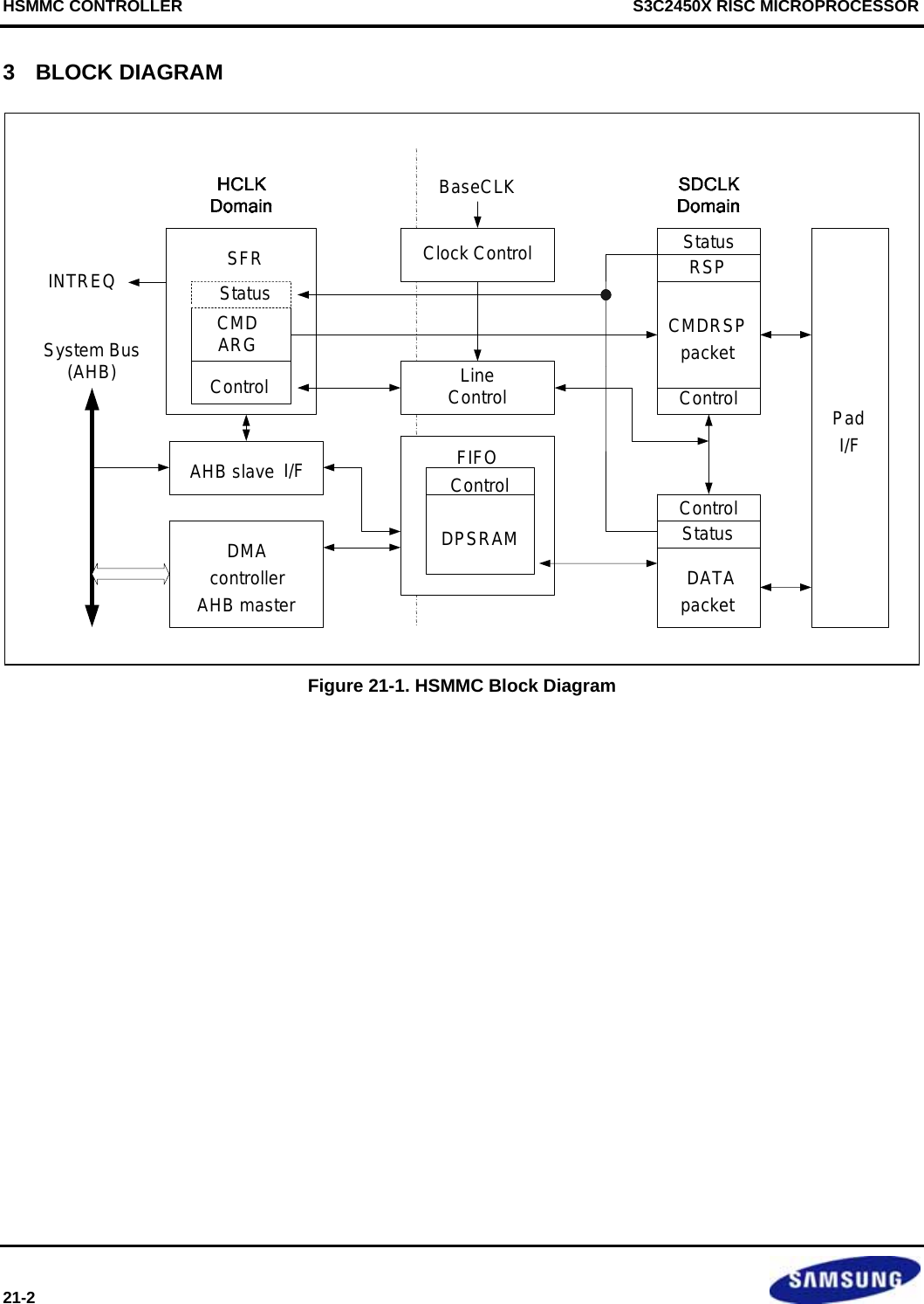
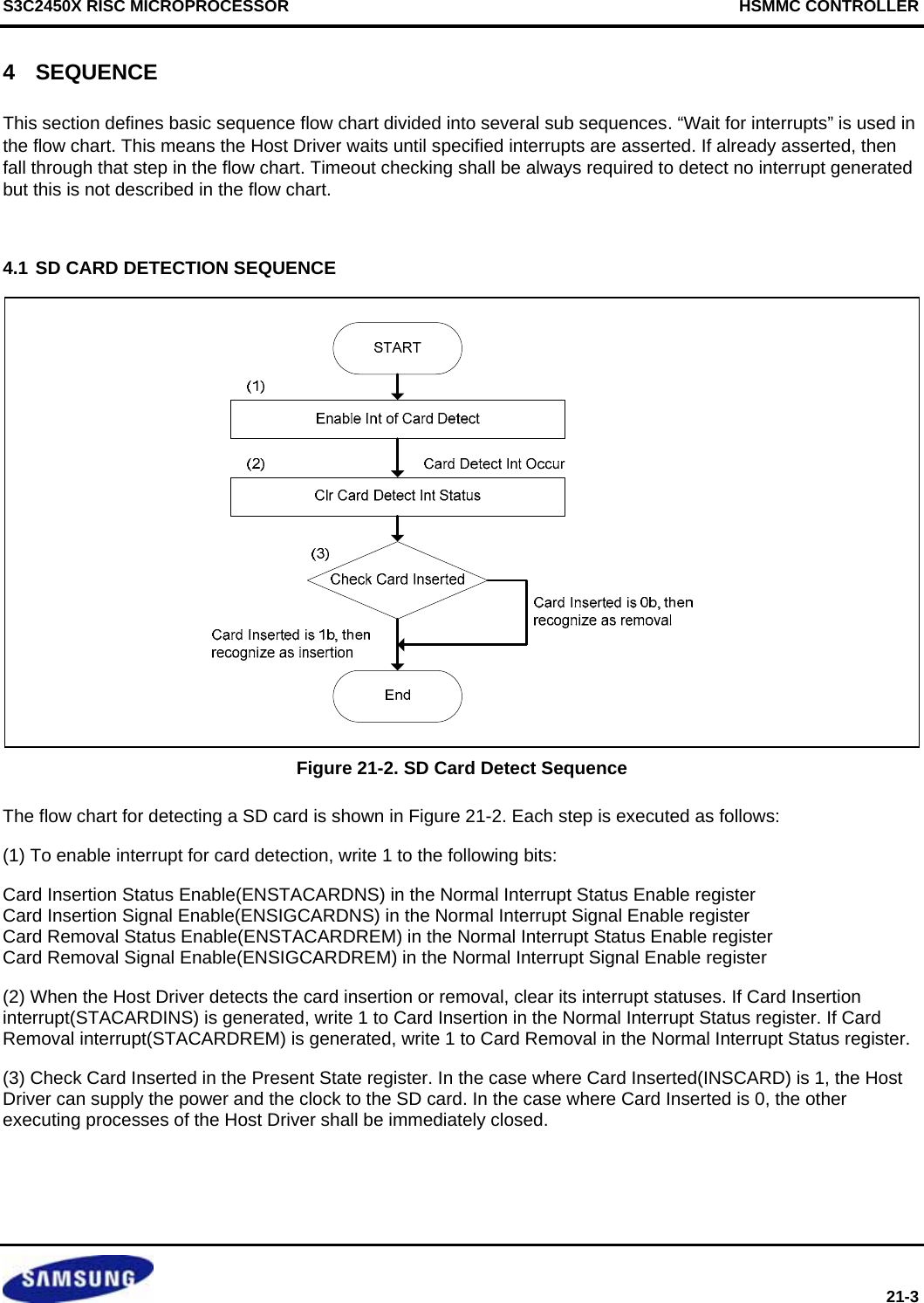
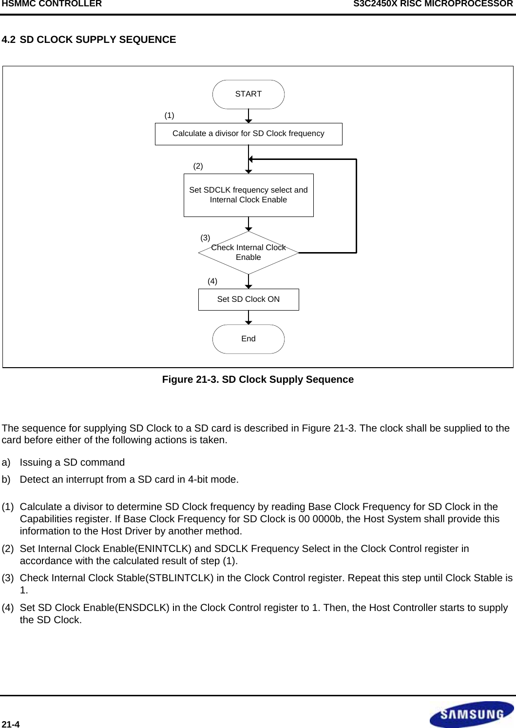
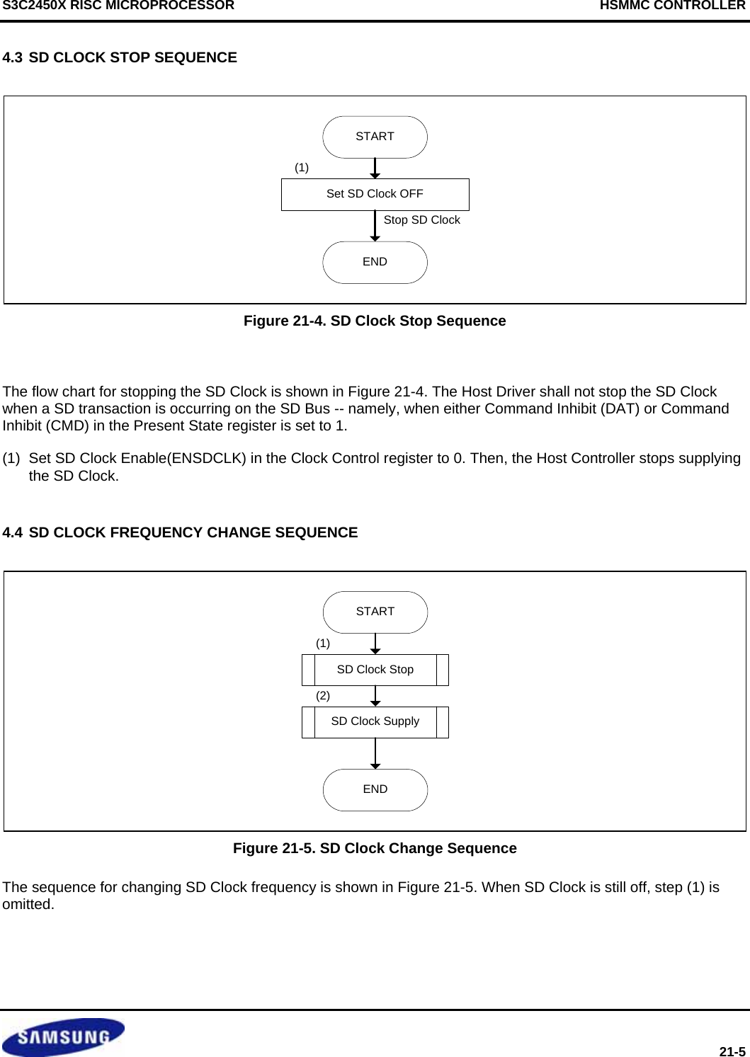
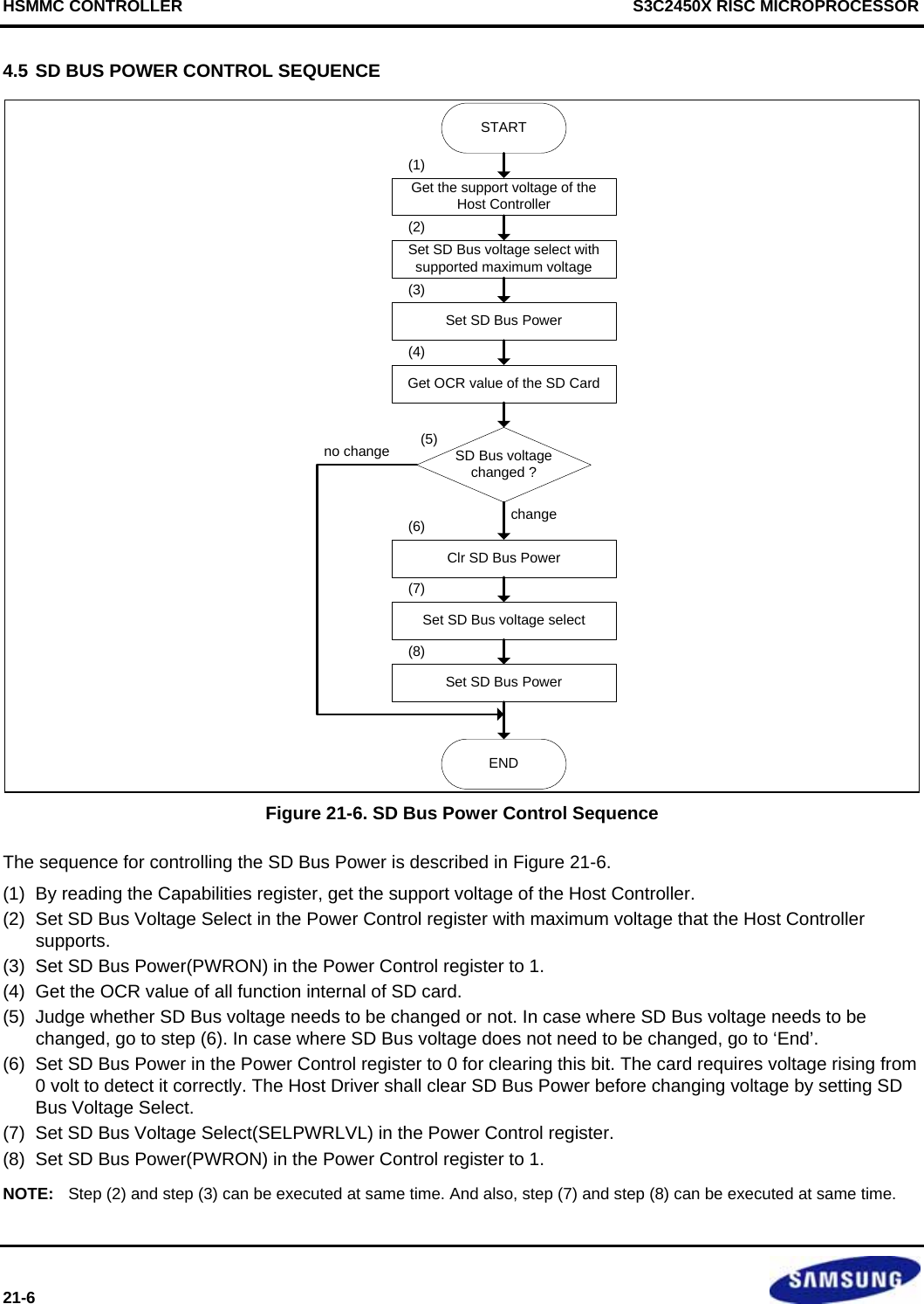
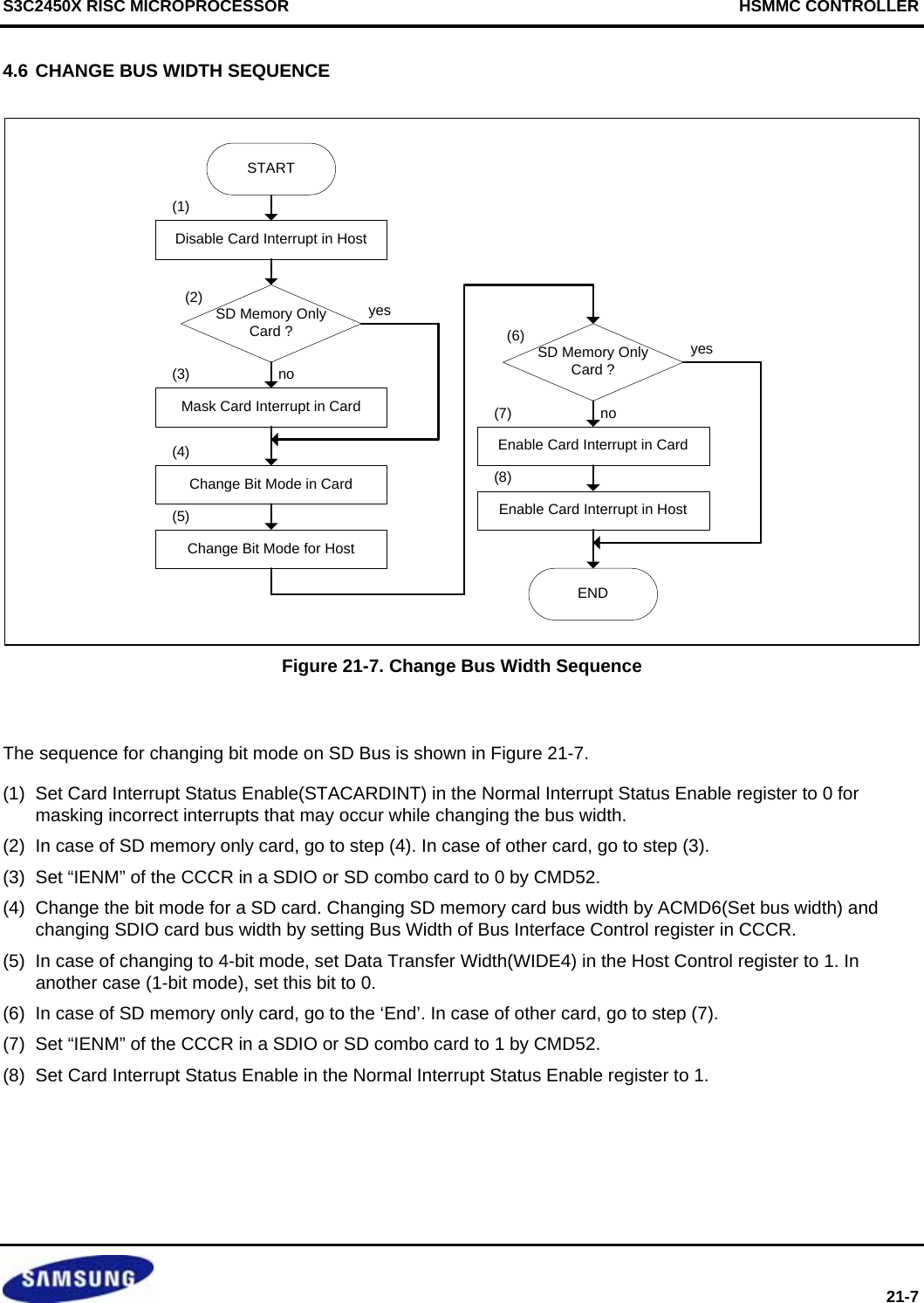
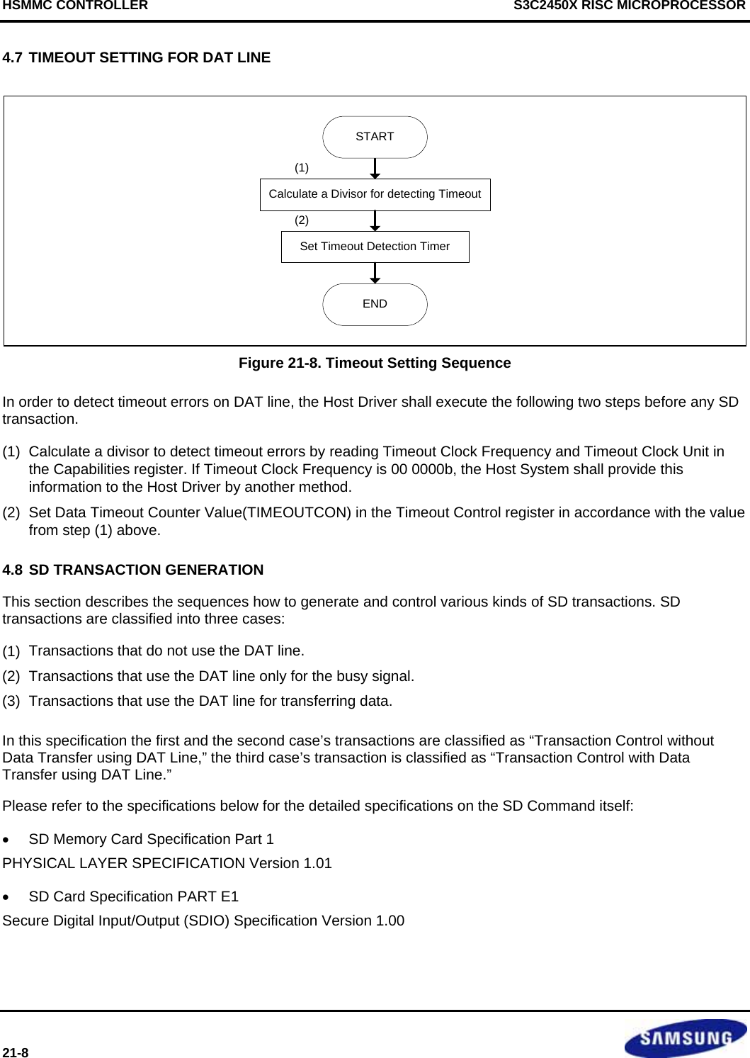
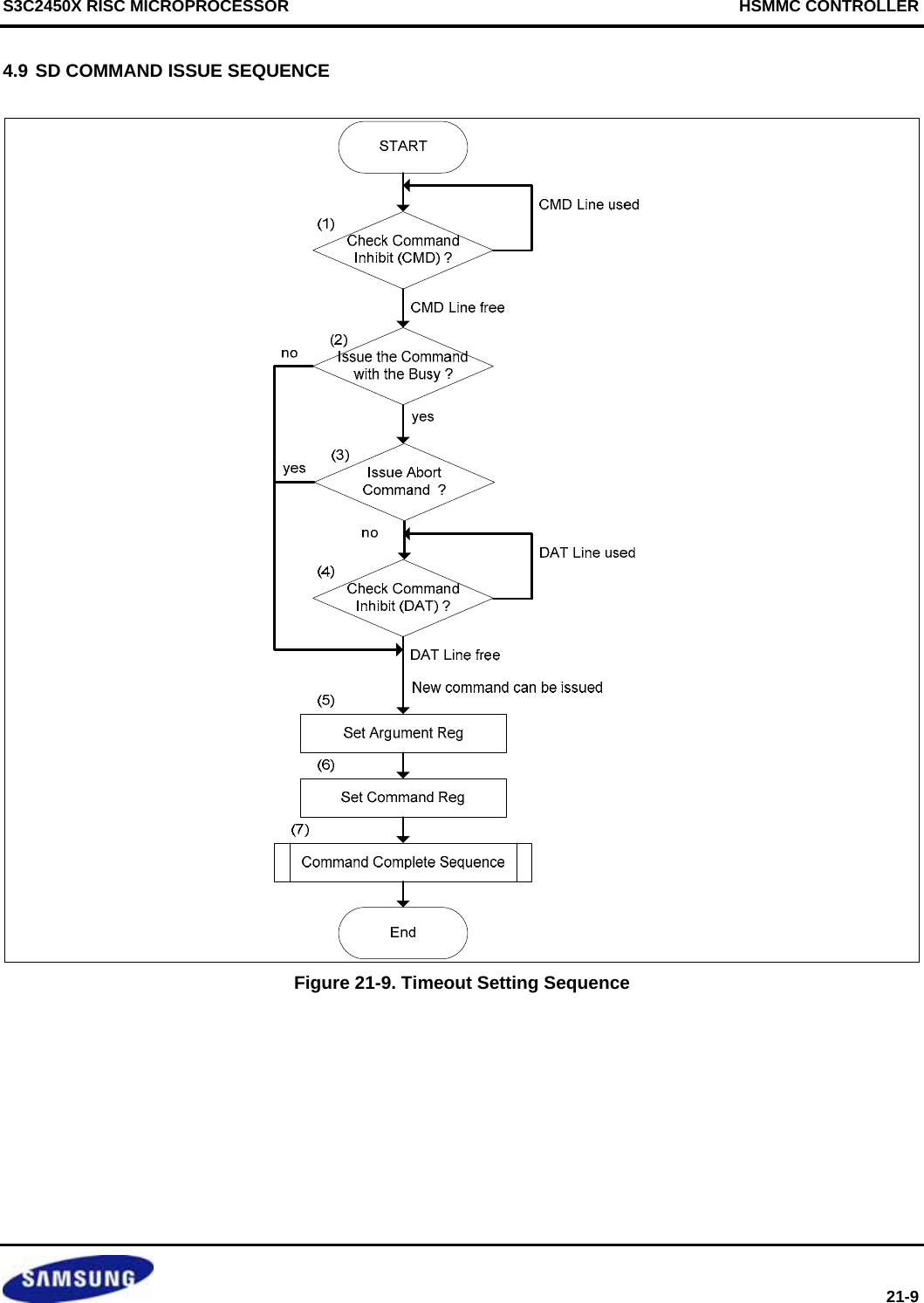
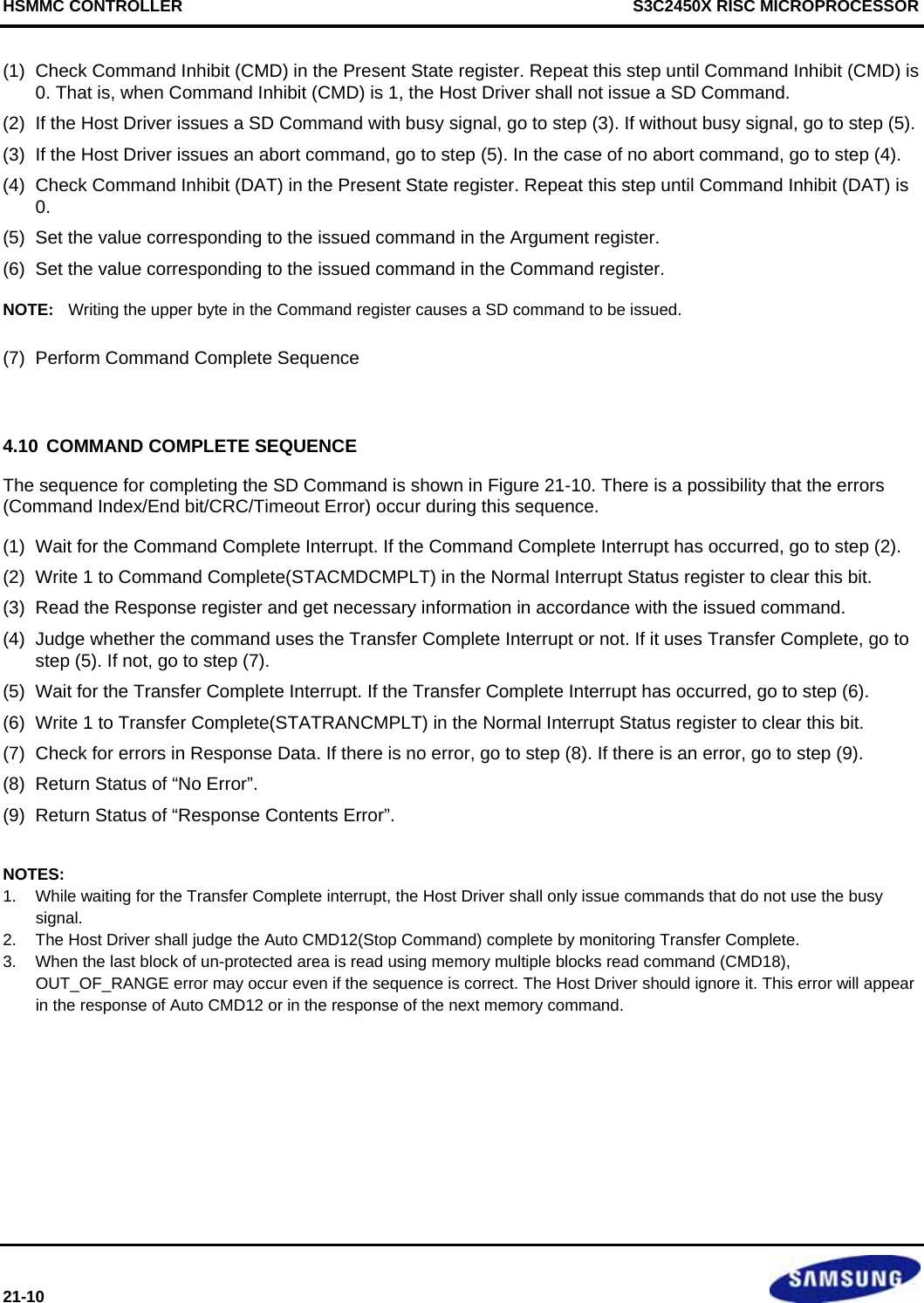
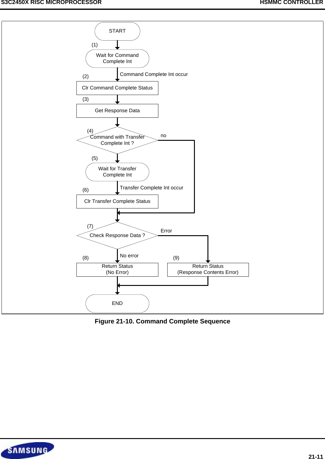
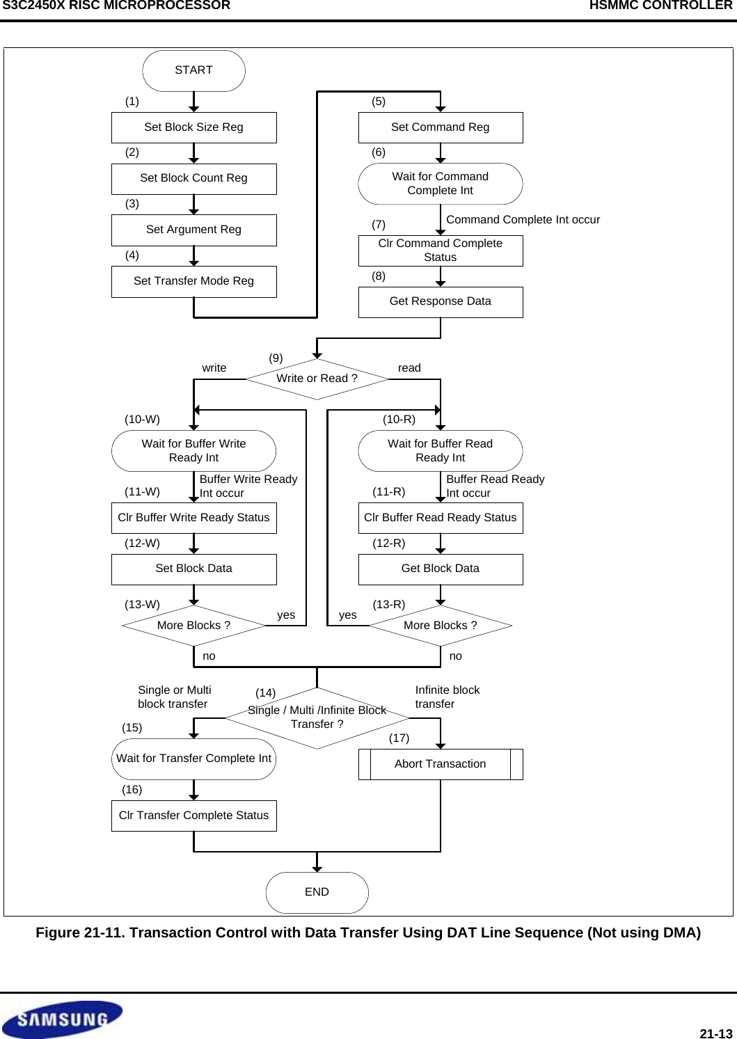
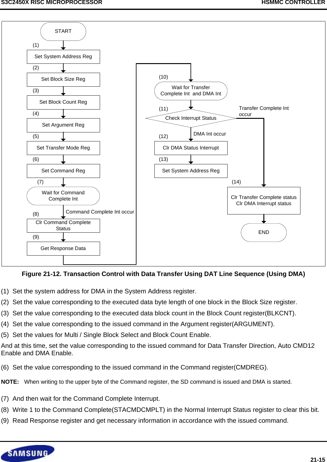
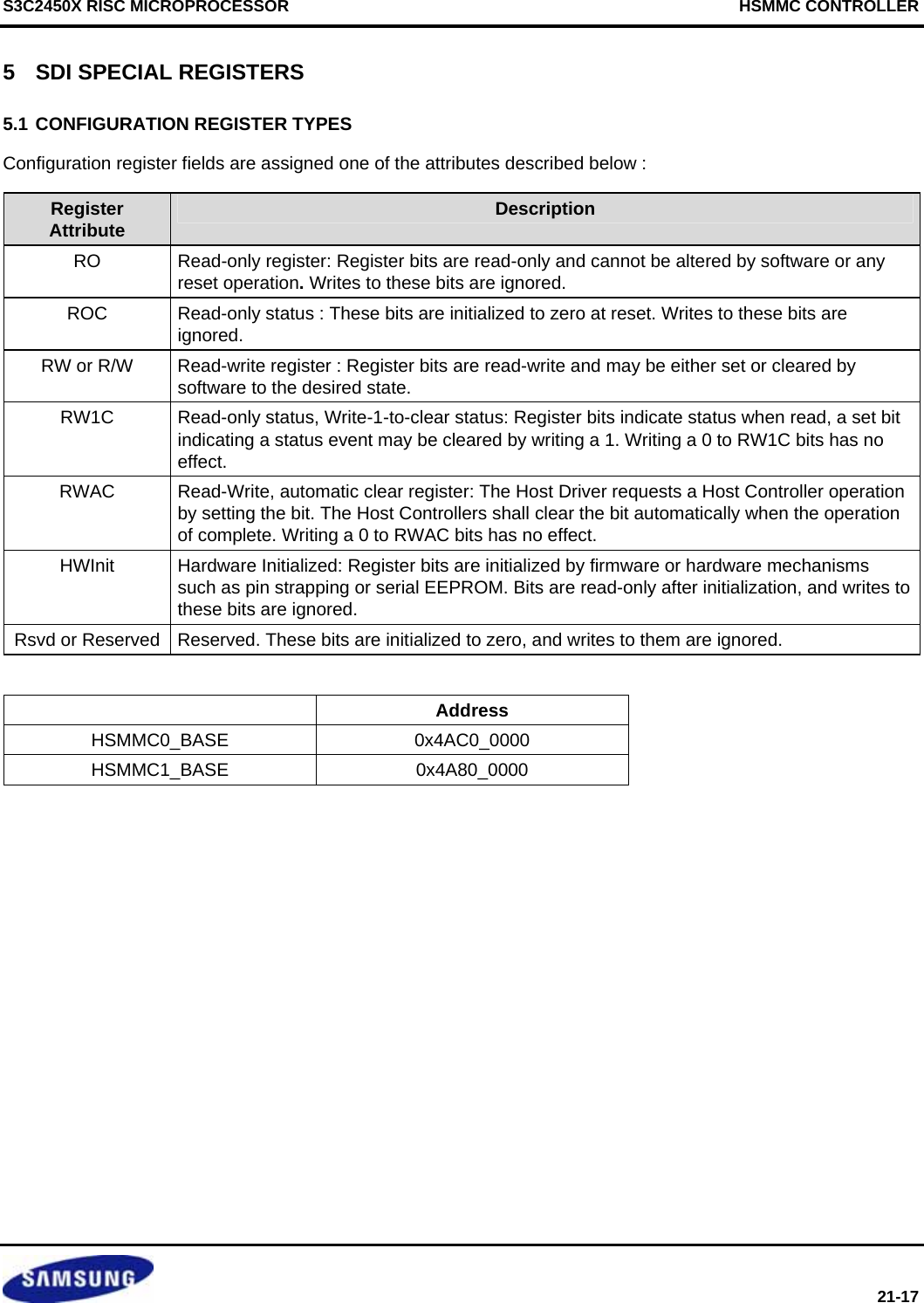
![HSMMC CONTROLLER S3C2450X RISC MICROPROCESSOR 21-18 5.2 SDMA SYSTEM ADDRESS REGISTER Register Address R/W Description Reset ValueSYSAD0 0X4AC00000 R/W System Address register (Channel 0) 0x0 SYSAD1 0X4A800000 R/W System Address register (Channel 1) 0x0 This register contains the physical system memory address used for DMA transfers. Name Bit Description Initial ValueSYSAD [31:0] SDMA System Address This register contains the system memory address for a DMA transfer. When the Host Controller stops a DMA transfer, this register shall point to the system address of the next contiguous data position. It can be accessed only if no transaction is executing (i.e., after a transaction has stopped). Read operations during transfers may return an invalid value. The Host Driver shall initialize this register before starting a DMA transaction. After DMA has stopped, the next system address of the next contiguous data position can be read from this register. The DMA transfer waits at the every boundary specified by the Host SDMA Buffer Boundary in the Block Size register. The Host Controller generates DMA Interrupt to request the Host Driver to update this register. The Host Driver set the next system address of the next data position to this register. When the most upper byte of this register (003h) is written, the Host Controller restarts the DMA transfer. When restarting DMA by the Resume command or by setting Continue Request in the Block Gap Control register, the Host Controller shall start at the next contiguous address stored here in the System Address register. 0x00](https://usermanual.wiki/Diasonic-Technology-Co/RVM-704M.Users-Manual/User-Guide-1826140-Page-516.png)
![S3C2450X RISC MICROPROCESSOR HSMMC CONTROLLER 21-19 5.3 BLOCK SIZE REGISTER This register is used to configure the number of bytes in a data block. Register Address R/W Description Reset ValueBLKSIZE0 0X4AC00004 R/W Host DMA Buffer Boundary and Transfer Block Size Register (Channel 0) 0x0 BLKSIZE1 0X4A800004 R/W Host DMA Buffer Boundary and Transfer Block Size Register (Channel 1) 0x0 Name Bit Description Initial Value [15] Reserved 0 BUFBOUND [14:12] Host DMA Buffer Boundary The large contiguous memory space may not be available in the virtual memory system. To perform long DMA transfer, System Address register shall be updated at every system memory boundary during DMA transfer. These bits specify the size of contiguous buffer in the system memory. The DMA transfer shall wait at the every boundary specified by these fields and the Host Controller generates the DMA Interrupt to request the Host Driver to update the System Address register. In case of this register is set to 0 (buffer size = 4K bytes), lower 12-bit of byte address points data in the contiguous buffer and the upper 20-bit points the location of the buffer in the system memory. The DMA transfer stops when the Host Controller detects carry out of the address from bit 11 to 12. These bits shall be supported when the DMA Support in the Capabilities register is set to 1 and this function is active when the DMA Enable in the Transfer Mode register is set to 1. 000b = 4K bytes (Detects A11 carry out) 001b = 8K bytes (Detects A12 carry out) 010b = 16K Bytes (Detects A13 carry out) 011b = 32K Bytes (Detects A14 carry out) 100b = 64K bytes (Detects A15 carry out) 101b = 128K Bytes (Detects A16 carry out) 110b = 256K Bytes (Detects A17 carry out) 111b = 512K Bytes (Detects A18 carry out) 0](https://usermanual.wiki/Diasonic-Technology-Co/RVM-704M.Users-Manual/User-Guide-1826140-Page-517.png)
![HSMMC CONTROLLER S3C2450X RISC MICROPROCESSOR 21-20 Name Bit Description Initial ValueBLKSIZE [11:0] Transfer Block Size This register specifies the block size of data transfers for CMD17, CMD18, CMD24, CMD25, and CMD53. Values ranging from 1 up to the maximum buffer size can be set. In case of memory, it shall be set up to 512 bytes. It can be accessed only if no transaction is executing (i.e., after a transaction has stopped). Read operations during transfers may return an invalid value, and write operations shall be ignored. 0200h = 512 Bytes 01FFh = 511 Bytes … 0004h = 4 Bytes 0003h = 3 Bytes 0002h = 2 Bytes 0001h = 1 Byte 0000h = No data transfer 0](https://usermanual.wiki/Diasonic-Technology-Co/RVM-704M.Users-Manual/User-Guide-1826140-Page-518.png)
![S3C2450X RISC MICROPROCESSOR HSMMC CONTROLLER 21-21 5.4 BLOCK COUNT REGISTER This register is used to configure the number of data blocks. Register Address R/W Description Reset ValueBLKCNT0 0X4AC00006 R/W Blocks Count For Current Transfer (Channel 0) 0x0 BLKCNT1 0X4A800006 R/W Blocks Count For Current Transfer (Channel 1) 0x0 Name Bit Description Initial ValueBLKCNT [15:0] Blocks Count For Current Transfer This register is enabled when Block Count Enable in the Transfer Mode register is set to 1 and is valid only for multiple block transfers. The Host Driver shall set this register to a value between 1 and the maximum block count. The Host Controller decrements the block count after each block transfer and stops when the count reaches zero. Setting the block count to 0 results in no data blocks being transferred. This register should be accessed only when no transaction is executing (i.e., after transactions are stopped). During data transfer, read operations on this register may return an invalid value and write operations are ignored. When saving transfer context as a result of a Suspend command, the number of blocks yet to be transferred can be determined by reading this register. When restoring transfer context prior to issuing a Resume command, the Host Driver shall restore the previously saved block count. FFFFh = 65535 blocks … … 0002h = 2 blocks 0001h = 1 block 0000h = Stop Count 0](https://usermanual.wiki/Diasonic-Technology-Co/RVM-704M.Users-Manual/User-Guide-1826140-Page-519.png)
![HSMMC CONTROLLER S3C2450X RISC MICROPROCESSOR 21-22 5.5 ARGUMENT REGISTER This register contains the SD Command Argument. Register Address R/W Description Reset ValueARGUMENT0 0X4AC00008 R/W Command Argument Register (Channel 0) 0x0 ARGUMENT1 0X4A800008 R/W Command Argument Register (Channel 1) 0x0 Name Bit Description Initial ValueARGUMENT [31:0] Command Argument The SD Command Argument is specified as bit39-8 of Command-Format in the SD Memory Card Physical Layer Specification. 0](https://usermanual.wiki/Diasonic-Technology-Co/RVM-704M.Users-Manual/User-Guide-1826140-Page-520.png)
![S3C2450X RISC MICROPROCESSOR HSMMC CONTROLLER 21-23 5.6 TRANSFER MODE REGISTER This register is used to control the operation of data transfers. The Host Driver shall set this register before issuing a command which transfers data (see Data Present Select in the Command register), or before issuing a Resume command. The Host Driver shall save the value of this register when the data transfer is suspended (as a result of a Suspend command) and restore it before issuing a Resume command. To prevent data loss, the Host Controller shall implement write protection for this register during data transactions. Writes to this register shall be ignored when the Command Inhibit (DAT) in the Present State register is 1. Register Address R/W Description Reset ValueTRNMOD0 0X4AC0000C R/W Transfer Mode Setting Register (Channel 0) 0x0 TRNMOD1 0X4A80000C R/W Transfer Mode Setting Register (Channel 1) 0x0 Name Bit Description Initial Value [15:10] Reserved 0 CCSCON [9:8] Command Completion Signal Control 00 = No CCS Operation (Normal operation, Not CE-ATA mode) 01 = Read or Write data transfer CCS enable (Only CE-ATA mode) 10 = Without data transfer CCS enable (Only CE-ATA mode) 11 = Abort Completion Signal (ACS) generation (Only CE-ATA mode) 0 [7:6] Reserved 0 MUL1SIN0 [5] Multi / Single Block Select This bit enables multiple block DAT line data transfers. For any other commands, this bit shall be set to 0. If this bit is 0, it is not necessary to set the Block Count register. (Refer to the Table below ″Determination of Transfer Type″ ) 1 = Multiple Block 0 = Single Block 0 RD1WT0 [4] Data Transfer Direction Select This bit defines the direction of DAT line data transfers. The bit is set to 1 by the Host Driver to transfer data from the SD card to the SD Host Controller and it is set to 0 for all other commands. 1 = Read (Card to Host) 0 = Write (Host to Card) 0 [3] Reserved 0 ENACMD12 [2] Auto CMD12 Enable Multiple block transfers for memory require CMD12 to stop the transaction. When this bit is set to 1, the Host Controller shall issue CMD12 automatically when last block transfer is completed. The Host Driver shall not set this bit to issue commands that do not require CMD12 to stop data transfer. 1 = Enable 0 = Disable 0](https://usermanual.wiki/Diasonic-Technology-Co/RVM-704M.Users-Manual/User-Guide-1826140-Page-521.png)
![HSMMC CONTROLLER S3C2450X RISC MICROPROCESSOR 21-24 Name Bit Description Initial ValueENBLKCNT [1] Block Count Enable This bit is used to enable the Block Count register, which is only relevant for multiple block transfers. When this bit is 0, the Block Count register is disabled, which is useful in executing an infinite transfer. (Refer to the Table below ″Determination of Transfer Type″ ) 1 = Enable 0 = Disable 0 ENDMA [0] DMA Enable This bit enables DMA functionality. DMA can be enabled only if it is supported as indicated in the DMA Support in the Capabilities register. If DMA is not supported, this bit is meaningless and shall always read 0. If this bit is set to 1, a DMA operation shall begin when the Host Driver writes to the upper byte of Command register (00Fh). 1 = Enable 0 = Disable 0 Table below shows the summary of how register settings determine types of data transfer. Table 21-1. Determination of Transfer Type Multi/Single Block Select Block Count Enable Block Count Function 0 Don′t care Don′t care Single Transfer 1 0 Don′t care Infinite Transfer 1 1 Not Zero Multiple Transfer 1 1 Zero Stop Multiple Transfer NOTE: For CE-ATA access, (Auto) CMD12 should be issued after Command Completion Signal Disable](https://usermanual.wiki/Diasonic-Technology-Co/RVM-704M.Users-Manual/User-Guide-1826140-Page-522.png)
![S3C2450X RISC MICROPROCESSOR HSMMC CONTROLLER 21-25 5.7 COMMAND REGISTER This register contains the SD Command Argument. Register Address R/W Description Reset ValueCMDREG0 0X4AC0000E R/W Command Register (Channel 0) 0x0 CMDREG1 0X4A80000E R/W Command Register (Channel 1) 0x0 The Host Driver shall check the Command Inhibit (DAT) bit and Command Inhibit (CMD) bit in the Present State register before writing to this register. Writing to the upper byte of this register triggers SD command generation. The Host Driver has the responsibility to write this register because the Host Controller does not protect for writing when Command Inhibit (CMD) is set. Name Bit Description Initial Value [15:14] Reserved CMDIDX [13:8] Command Index These bits shall be set to the command number (CMD0-63, ACMD0-63) that is specified in bits 45-40 of the Command-Format in the SD Memory Card Physical Layer Specification and SDIO Card Specification. CMDTYP [7:6] Command Type There are three types of special commands: Suspend, Resume and Abort. These bits shall be set to 00b for all other commands. • Suspend Command If the Suspend command succeeds, the Host Controller shall assume the SD Bus has been released and that it is possible to issue the next command which uses the DAT line. The Host Controller shall de-assert Read Wait for read transactions and stop checking busy for write transactions. The interrupt cycle shall start, in 4-bit mode. If the Suspend command fails, the Host Controller shall maintain its current state, and the Host Driver shall restart the transfer by setting Continue Request in the Block Gap Control register. • Resume Command The Host Driver re-starts the data transfer by restoring the registers in the range of 000-00Dh. (Refer to Suspend and Resume mechanism) The Host Controller shall check for busy before starting write transfers. • Abort Command If this command is set when executing a read transfer, the Host Controller shall stop reads to the buffer. If this command is set when executing a write transfer, the Host Controller shall stop driving the DAT line. After issuing the Abort command, the Host Driver should issue a software reset. (Refer to Abort Transaction) 11b = Abort CMD12, CMD52 for writing “I/O Abort” in CCCR 10b = Resume CMD52 for writing “Function Select” in CCCR 01b = Suspend CMD52 for writing “Bus Suspend” in CCCR 00b = Normal Other commands](https://usermanual.wiki/Diasonic-Technology-Co/RVM-704M.Users-Manual/User-Guide-1826140-Page-523.png)
![HSMMC CONTROLLER S3C2450X RISC MICROPROCESSOR 21-26 Name Bit Description Initial ValueDATAPRNT [5] Data Present Select This bit is set to 1 to indicate that data is present and shall be transferred using the DAT line. It is set to 0 for the following: (1) Commands using only CMD line (ex. CMD52). (2) Commands with no data transfer but using busy signal on DAT[0] line (R1b or R5b ex. CMD38) (3) Resume command 1 = Data Present 0 = No Data Present ENCMDIDX [4] Command Index Check Enable If this bit is set to 1, the Host Controller shall check the Index field in the response to see if it has the same value as the command index. If it is not, it is reported as a Command Index Error. If this bit is set to 0, the Index field is not checked. 1 = Enable 0 = Disable ENCMDCRC [3] Command CRC Check Enable If this bit is set to 1, the Host Controller shall check the CRC field in the response. If an error is detected, it is reported as a Command CRC Error. If this bit is set to 0, the CRC field is not checked. The number of bits checked by the CRC field value changes according to the length of the response. 1 = Enable 0 = Disable [2] Reserved RSPTYP [1:0] Response Type Select 00 = No Response 01 = Response Length 136 10 = Response Length 48 11 = Response Length 48 check Busy after response Table 21-2. Relation Between Parameters and the Name of Response Type Response Type Index Check Enable CRC Check Enable Name of Response Type 00 0 0 No Response 01 0 1 R2 10 0 0 R3, R4 10 1 1 R1, R6, R5, R7 11 1 1 R1b, R5b These bits determine Response types.](https://usermanual.wiki/Diasonic-Technology-Co/RVM-704M.Users-Manual/User-Guide-1826140-Page-524.png)
![S3C2450X RISC MICROPROCESSOR HSMMC CONTROLLER 21-27 NOTES: 1. In the SDIO specification, response type notation of R5b is not defined. R5 includes R5b in the SDIO specification. But R5b is defined in this specification to specify the Host Controller shall check busy after receiving response. For example, usually CMD52 is used as R5 but I/O abort command shall be used as R5b. 2. For CMD52 to read BS after writing "Bus Suspend," Command Type should be "Suspend" as well. 5.8 RESPONSE REGISTER This register is used to store responses from SD cards. Register Address R/W Description Reset ValueRSPREG0_0 0X4AC00010 ROC Response Register 0 (Channel 0) 0x0 RSPREG1_0 0X4AC00014 ROC Response Register 1 (Channel 0) 0x0 RSPREG2_0 0X4AC00018 ROC Response Register 2 (Channel 0) 0x0 RSPREG3_0 0X4AC0001C ROC Response Register 3 (Channel 0) 0x0 Register Address R/W Description Reset ValueRSPREG0_1 0X4A800010 ROC Response Register 0 (Channel 1) 0x0 RSPREG1_1 0X4A800014 ROC Response Register 1 (Channel 1) 0x0 RSPREG2_1 0X4A800018 ROC Response Register 2 (Channel 1) 0x0 RSPREG3_1 0X4A80001C ROC Response Register 3 (Channel 1) 0x0 Name Bit Description Initial ValueCMDRSP [127:0] Command Response The Table below describes the mapping of command responses from the SD Bus to this register for each response type. In the table, R[] refers to a bit range within the response data as transmitted on the SD Bus, REP[] refers to a bit range within the Response register. 128-bit Response bit order : {RSPREG3, RSPREG2, RSPREG1, RSPREG0} Table 21-3. Response Bit Definition for Each Response Type. Kind of Response Meaning of Response Response Field Response RegisterR1, R1b (normal response) Card Status R [39:8] REP [31:0] R1b (Auto CMD12 response) Card Status for Auto CMD12 R [39:8] REP [127:96] R2 (CID, CSD register) CID or CSD reg. incl. R [127:8] REP [119:0] R3 (OCR register) OCR register for memory R [39:8] REP [31:0] R4 (OCR register) OCR register for I/O etc R [39:8] REP [31:0] R5,R5b SDIO response R [39:8] REP [31:0] R6 (Published RCA response) New published RCA[31:16] etc R [39:8] REP [31:0] R7 ? R [39:8] REP [31:0]](https://usermanual.wiki/Diasonic-Technology-Co/RVM-704M.Users-Manual/User-Guide-1826140-Page-525.png)
![HSMMC CONTROLLER S3C2450X RISC MICROPROCESSOR 21-28 The Response Field indicates bit positions of “Responses” defined in the PHYSICAL LAYER SPECIFICATION Version 1.01. The Table (upper) shows that most responses with a length of 48 (R[47:0]) have 32 bits of the response data (R[39:8]) stored in the Response register at REP[31:0]. Responses of type R1b (Auto CMD12 responses) have response data bits R[39:8] stored in the Response register at REP[127:96]. Responses with length 136 (R[135:0]) have 120 bits of the response data (R[127:8]) stored in the Response register at REP[119:0]. To be able to read the response status efficiently, the Host Controller only stores part of the response data in the Response register. This enables the Host Driver to efficiently read 32 bits of response data in one read cycle on a 32-bit bus system. Parts of the response, the Index field and the CRC, are checked by the Host Controller (as specified by the Command Index Check Enable and the Command CRC Check Enable bits in the Command register) and generate an error interrupt if an error is detected. The bit range for the CRC check depends on the response length. If the response length is 48, the Host Controller shall check R[47:1], and if the response length is 136 the Host Controller shall check R[119:1]. Since the Host Controller may have a multiple block data DAT line transfer executing concurrently with a CMD_wo_DAT command, the Host Controller stores the Auto CMD12 response in the upper bits (REP[127:96]) of the Response register. The CMD_wo_DAT response is stored in REP[31:0]. This allows the Host Controller to avoid overwriting the Auto CMD12 response with the CMD_wo_DAT and vice versa. When the Host Controller modifies part of the Response register, as shown in the Table above, it shall preserve the unmodified bits. NOTE: CMD_wo_DAT (Command without Data line) means the command not to use data line. The command set of this type depends on the card type (MMC, SD/SDIO or CE-ATA). Generally, the command using data line receives contents through “Buffer Data Port Register”, but the command without using data line receives contents through “RESPONSE register” in the Host Controller.](https://usermanual.wiki/Diasonic-Technology-Co/RVM-704M.Users-Manual/User-Guide-1826140-Page-526.png)
![S3C2450X RISC MICROPROCESSOR HSMMC CONTROLLER 21-29 5.9 BUFFER DATA PORT REGISTER 32-bit data port register to access internal buffer. Register Address R/W Description Reset ValueBDATA0 0X4AC00020 R/W Buffer Data Register (Channel 0) − BDATA1 0X4A800020 R/W Buffer Data Register (Channel 1) − Name Bit Description Initial ValueBUFDAT [31:0] Buffer Data The Host Controller buffer can be accessed through this 32-bit Data Port register. − Detailed documents are to be copied from SD Host Standard Spec.](https://usermanual.wiki/Diasonic-Technology-Co/RVM-704M.Users-Manual/User-Guide-1826140-Page-527.png)
![HSMMC CONTROLLER S3C2450X RISC MICROPROCESSOR 21-30 5.10 PRESENT STATE REGISTER This register contains the SD Command Argument. Register Address R/W Description Reset ValuePRNSTS0 0X4AC00024 RO/ROC Present State Register (Channel 0) 0x000A0000PRNSTS1 0X4A800024 RO/ROC Present State Register (Channel 1) 0x000A0000 Name Bit Description Initial Value [31:25] Reserved 0 PRNTCMD [24] CMD Line Signal Level (RO) This status is used to check the CMD line level to recover from errors, and for debugging. Note: CMD port is mapped to SDx_CMD pin 0 PRNTDAT [23:20] DAT[3:0] Line Signal Level (RO) This status is used to check the DAT line level to recover from errors, and for debugging. This is especially useful in detecting the busy signal level from DAT[0]. D23 = DAT[3] D22 = DAT[2] D21 = DAT[1] D20 = DAT[0] Note: DAT port is mapped to SDx_DAT pin Line State PRNTWP [19] Write Protect Switch Pin Level (RO) The Write Protect Switch is supported for memory and combo cards. This bit reflects the SDWP# pin. 1 = Write enabled (SDWP#=1) 0 = Write protected (SDWP#=0) Note: SDWP# of channel 0 is fixed to High. 1 PRNTCD [18] Card Detect Pin Level (RO) This bit reflects the inverse value of the SDCD# pin. Debouncing is not performed on this bit. This bit may be valid when Card State Stable is set to 1, but it is not guaranteed because of propagation delay. Use of this bit is limited to testing since it must be debounced by software. 1 = Card present (SDCD#=0) 0 = No card present (SDCD#=1) Note: SDCD# of Channel 0 is fixed to LOW. Line State STBLCARD [17] Card State Stable (RO) This bit is used for testing. If it is 0, the Card Detect Pin Level is not stable. If this bit is set to 1, it means the Card Detect Pin Level is stable. No Card state can be detected by this bit is set to 1 and Card Inserted is set to 0. The Software Reset For All in the Software Reset register shall not affect this bit. 1 = No Card or Inserted 1 (After Reset)](https://usermanual.wiki/Diasonic-Technology-Co/RVM-704M.Users-Manual/User-Guide-1826140-Page-528.png)
![S3C2450X RISC MICROPROCESSOR HSMMC CONTROLLER 21-31 Name Bit Description Initial Value0 = Reset or Debouncing INSCARD [16] Card Inserted (RO) This bit indicates whether a card has been inserted. The Host Controller shall debounce this signal so that the Host Driver will not need to wait for it to stabilize. Changing from 0 to 1 generates a Card Insertion interrupt in the Normal Interrupt Status register and changing from 1 to 0 generates a Card Removal interrupt in the Normal Interrupt Status register. The Software Reset For All in the Software Reset register shall not affect this bit. If a card is removed while its power is on and its clock is oscillating, the Host Controller shall clear SD Bus Power in the Power Control register and SD Clock Enable in the Clock Control register. When this bit is changed from 1 to 0, the Host Controller shall immediately stop driving CMD and DAT[3:0] (tri-state). In addition, the Host Driver should clear the Host Controller by the Software Reset For All in Software Reset register. The card detect is active regardless of the SD Bus Power. 1 = Card Inserted 0 = Reset or Debouncing or No Card 0 [15:14] Reserved DIFF4W [13] FIFO Pointer Difference 4-Word (ROC) When the difference of the address pointer between AHB side and SD side is more than or equal to 4-word, this status bit is set to HIGH. When others clears automatically. Write(Tx) mode : when this bit is HIGH, more than or equal to 4-word can be written by CPU side. Read(Rx) mode : when this bit is HIGH, more than or equal to 4-word can be read by CPU side. 0 DIFF1W [12] FIFO Pointer Difference 1-Word (ROC) When the difference of the address pointer between AHB side and SD side is more than or equal to 1-word, this status bit is set to HIGH. When others clears automatically. Write(Tx) mode : when this bit is HIGH, more than or equal to 1-word can be written by CPU side. Read(Rx) mode : when this bit is HIGH, more than or equal to 1-word can be read by CPU side. 0 BUFRDRDY [11] Buffer Read Enable (ROC) This status is used for non-DMA read transfers. The Host Controller may implement multiple buffers to transfer data efficiently. This read only flag indicates that valid data exists in the host side buffer status. If this bit is 1, readable data exists in the buffer. A change of this bit from 1 to 0 occurs when all the block data is read from the buffer. A change of this bit from 0 to 1 occurs when block data is ready in the buffer and generates the Buffer Read Ready interrupt. 1 = Read enable 0 = Read disable 0](https://usermanual.wiki/Diasonic-Technology-Co/RVM-704M.Users-Manual/User-Guide-1826140-Page-529.png)
![HSMMC CONTROLLER S3C2450X RISC MICROPROCESSOR 21-32 Name Bit Description Initial ValueBUFWTRDY [10] Buffer Write Enable (ROC) This status is used for non-DMA write transfers. The Host Controller can implement multiple buffers to transfer data efficiently. This read only flag indicates if space is available for write data. If this bit is 1, data can be written to the buffer. A change of this bit from 1 to 0 occurs when all the block data is written to the buffer. A change of this bit from 0 to 1 occurs when top of block data can be written to the buffer and generates the Buffer Write Ready interrupt. 1 = Write enable 0 = Write disable 0 RDTRANACT [9] Read Transfer Active (ROC) This status is used for detecting completion of a read transfer. This bit is set to 1 for either of the following conditions: (1) After the end bit of the read command. (2) When writing a 1 to Continue Request in the Block Gap Control register to restart a read transfer. This bit is cleared to 0 for either of the following conditions:: (1) When the last data block as specified by block length is transferred to the System. (2) When all valid data blocks have been transferred to the System and no current block transfers are being sent as a result of the Stop At Block Gap Request being set to 1. A Transfer Complete interrupt is generated when this bit changes to 0. 1 = Transferring data 0 = No valid data 0 WTTRANACT [8] Write Transfer Active (ROC) This status indicates a write transfer is active. If this bit is 0, it means no valid write data exists in the Host Controller. This bit is set in either of the following cases: (1) After the end bit of the write command. (2) When writing a 1 to Continue Request in the Block Gap Control register to restart a write transfer. This bit is cleared in either of the following cases: (1) After getting the CRC status of the last data block as specified by the transfer count (Single and Multiple) (2) After getting the CRC status of any block where data transmission is about to be stopped by a Stop At Block Gap Request. During a write transaction, a Block Gap Event interrupt is generated when this bit is changed to 0, as result of the Stop At Block Gap Request being set. This status is useful for the Host Driver in determining when to issue commands during write busy. 1 = Transferring data 0 = No valid data 0](https://usermanual.wiki/Diasonic-Technology-Co/RVM-704M.Users-Manual/User-Guide-1826140-Page-530.png)
![S3C2450X RISC MICROPROCESSOR HSMMC CONTROLLER 21-33 Name Bit Description Initial Value [7:3] Reserved 0 DATLINEACT [2] DAT Line Active (ROC) This bit indicates whether one of the DAT line on SD Bus is in use. (a) In the case of read transactions This status indicates if a read transfer is executing on the SD Bus. Changes in this value from 1 to 0 between data blocks generate a Block Gap Event interrupt in the Normal Interrupt Status register. This bit shall be set in either of the following cases: (1) After the end bit of the read command. (2) When writing a 1 to Continue Request in the Block Gap Control register to restart a read transfer. This bit shall be cleared in either of the following cases: (1) When the end bit of the last data block is sent from the SD Bus to the Host Controller. (2) When beginning a wait read transfer at a stop at the block gap initiated by a Stop At Block Gap Request. The Host Controller shall wait at the next block gap by driving Read Wait at the start of the interrupt cycle. If the Read Wait signal is already driven (data buffer cannot receive data), the Host Controller can wait for current block gap by continuing to drive the Read Wait signal. It is necessary to support Read Wait in order to use the suspend / resume function. (b) In the case of write transactions This status indicates that a write transfer is executing on the SD Bus. Changes in this value from 1 to 0 generate a Transfer Complete interrupt in the Normal Interrupt Status register. This bit shall be set in either of the following cases: (1) After the end bit of the write command. (2) When writing to 1 to Continue Request in the Block Gap Control register to continue a write transfer. This bit shall be cleared in either of the following cases: (1) When the SD card releases write busy of the last data block the Host Controller shall also detect if output is not busy. If SD card does not drive busy signal for 8 SD Clocks, the Host Controller shall consider the card drive “Not Busy”. (2) When the SD card releases write busy prior to waiting for write transfer as a result of a Stop At Block Gap Request. 1 = DAT Line Active 0 = DAT Line Inactive 0 CMDINHDAT [1] Data Inhibit (DAT) (ROC) This status bit is generated if either the DAT Line Active or the Read Transfer Active is set to 1. If this bit is 0, it indicates the Host Controller can issue the next SD Command. Commands with busy signal belong to Command Inhibit (DAT) (ex. R1b, R5b type). 0](https://usermanual.wiki/Diasonic-Technology-Co/RVM-704M.Users-Manual/User-Guide-1826140-Page-531.png)
![HSMMC CONTROLLER S3C2450X RISC MICROPROCESSOR 21-34 Name Bit Description Initial ValueChanging from 1 to 0 generates a Transfer Complete interrupt in the Normal Interrupt Status register. Note: The SD Host Driver can save registers in the range of 000-00Dh for a suspend transaction after this bit has changed from 1 to 0. 1 = Cannot issue command which uses the DAT line 0 = Can issue command which uses the DAT line CMDINHCMD [0] Command Inhibit (CMD) (ROC) If this bit is 0, it indicates the CMD line is not in use and the Host Controller can issue a SD Command using the CMD line. This bit is set immediately after the Command register (00Fh) is written. This bit is cleared when the command response is received. Even if the Command Inhibit (DAT) is set to 1, Commands using only the CMD line can be issued if this bit is 0. Changing from 1 to 0 generates a Command Complete interrupt in the Normal Interrupt Status register. If the Host Controller cannot issue the command because of a command conflict error (Refer to Command CRC Error) or because of Command Not Issued By Auto CMD12 Error, this bit shall remain 1 and the Command Complete is not set. Status issuing Auto CMD12 is not read from this bit. 1 = Cannot issue command 0 = Can issue command using only CMD line 0 NOTE: Buffer Write Enable in Present register should not be asserted for DMA transfers since it generates Buffer Write Ready interrupt ResetPower ONDebouncingOnce debouncingclock becomes validCard InsertedNo CardSDCD=1SDCD=0StableStable Figure 21-13. Card Detect State The above Figure shows the state definitions of hardware that handles “Debouncing”.](https://usermanual.wiki/Diasonic-Technology-Co/RVM-704M.Users-Manual/User-Guide-1826140-Page-532.png)
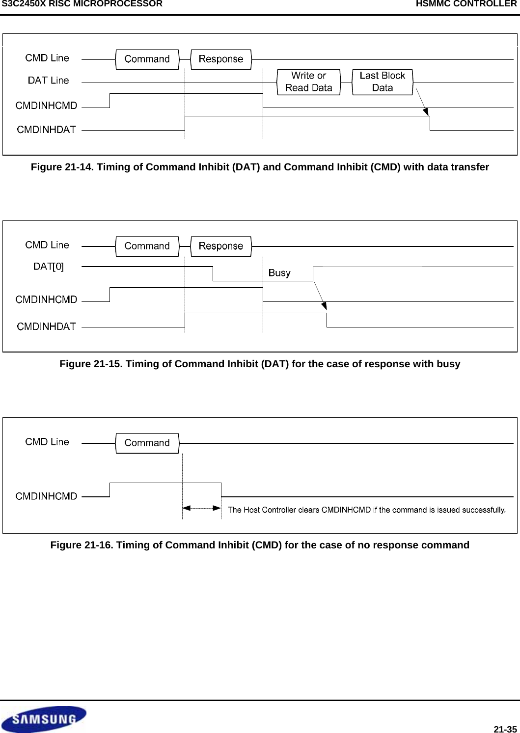
![HSMMC CONTROLLER S3C2450X RISC MICROPROCESSOR 21-36 5.11 HOST CONTROL REGISTER This register contains the SD Command Argument. Register Address R/W Description Reset ValueHOSTCTL0 0X4AC00028 R/W Present State Register (Channel 0) 0x0 HOSTCTL1 0X4A800028 R/W Present State Register (Channel 1) 0x0 Name Bit Description Initial ValueCDSIGSEL [7] Reserved This field should be fixed to LOW 0 CDTESTLVL [6] Reserved This field should be fixed to LOW 0 WIDE8 [5] Extended Data Transfer Width (It is for MMC 8bit card.) 1 = 8 bit operation 0 = the bit width is designated by the bit 1 (Data Transfer Width) 0 DMASEL [4:3] DMA Select One of supported DMA modes can be selected. The host driver shall check support of DMA modes by referring the Capabilities register. Use of selected DMA is determined by DMA Enable of the Transfer Mode register. 00 = SDMA is selected 01 = Reserved 10 = 32-bit Address ADMA2 is selected 11 = 64-bit Address ADMA2 is selected (Not supported) 0 ENHIGHSPD [2] High Speed Enable This bit is optional. Before setting this bit, the Host Driver shall check the High Speed Support in the Capabilities register. If this bit is set to 0 (default), the Host Controller outputs CMD line and DAT lines at the falling edge of the SD Clock (up to 25MHz). If this bit is set to 1, the Host Controller outputs CMD line and DAT lines at the rising edge of the SD Clock (up to 50MHz). 1 = High Speed mode 0 = Normal Speed mode 0 WIDE4 [1] Data Transfer Width This bit selects the data width of the Host Controller. The Host Driver shall set it to match the data width of the SD card. 1 = 4-bit mode 0 = 1-bit mode 0 ONLED [0] LED Control This bit is used to caution the user not to remove the card while the SD card is being accessed. If the software is going to issue multiple SD commands, this bit can be set during all these transactions. It is not necessary to change for each transaction. 1 = LED on 0 = LED off Note: LED port is mapped to SD0_LED pin 0 NOTE: Card Detect Pin Level does not simply reflect SDCD# pin, but chooses from SDCD, DAT[3], or CDTestlvl depending on CDSSigSel and SDCDSel values.](https://usermanual.wiki/Diasonic-Technology-Co/RVM-704M.Users-Manual/User-Guide-1826140-Page-534.png)
![S3C2450X RISC MICROPROCESSOR HSMMC CONTROLLER 21-37 5.12 POWER CONTROL REGISTER This register contains the SD Command Argument. Register Address R/W Description Reset ValuePWRCON0 0X4AC00029 R/W Present State Register (Channel 0) 0x0 PWRCON1 0X4A800029 R/W Present State Register (Channel 1) 0x0 Name Bit Description Initial Value [7:4] Reserved SELPWRLVL [3:1] SD Bus Voltage Select By setting these bits, the Host Driver selects the voltage level for the SD card. Before setting this register, the Host Driver shall check the Voltage Support bits in the Capabilities register. If an unsupported voltage is selected, the Host System shall not supply SD Bus voltage. 111b = 3.3V (Typ.) 110b = 3.0V (Typ.) 101b = 1.8V (Typ.) 100b − 000b = Reserved 0 PWRON [0] SD Bus Power Before setting this bit, the SD Host Driver shall set SD Bus Voltage Select. If the Host Controller detects the No Card state, this bit shall be cleared. If this bit is cleared, the Host Controller shall immediately stop driving CMD and DAT[3:0] (tri-state) and drive SDCLK to low level. 1 = Power on 0 = Power off 0](https://usermanual.wiki/Diasonic-Technology-Co/RVM-704M.Users-Manual/User-Guide-1826140-Page-535.png)
![HSMMC CONTROLLER S3C2450X RISC MICROPROCESSOR 21-38 5.13 BLOCK GAP CONTROL REGISTER This register contains the SD Command Argument. Register Address R/W Description Reset ValueBLKGAP0 0X4AC0002A R/W Block Gap Control Register (Channel 0) 0x0 BLKGAP1 0X4A80002A R/W Block Gap Control Register (Channel 1) 0x0 Name Bit Description Initial Value [7:4] Reserved 0 ENINTBGAP [3] Interrupt At Block Gap This bit is valid only in 4-bit mode of the SDIO card and selects a sample point in the interrupt cycle. Setting to 1 enables interrupt detection at the block gap for a multiple block transfer. Setting to 0 disables interrupt detection during a multiple block transfer. If the SD card cannot signal an interrupt during a multiple block transfer, this bit should be set to 0. When the Host Driver detects an SD card insertion, it shall set this bit according to the CCCR of the SDIO card. (RW) 1 = Enabled 0 = Disabled 0 ENRWAIT [2] Read Wait Control The read wait function is optional for SDIO cards. If the card supports read wait, set this bit to enable use of the read wait protocol to stop read data using the DAT[2] line. Otherwise the Host Controller has to stop the SD Clock to hold read data, which restricts commands generation. When the Host Driver detects an SD card insertion, it shall set this bit according to the CCCR of the SDIO card. If the card does not support read wait, this bit shall never be set to 1 otherwise DAT line conflict may occur. If this bit is set to 0, Suspend/Resume cannot be supported. (RW) 1 = Enable Read Wait Control 0 = Disable Read Wait Control 0 CONTREQ [1] Continue Request This bit is used to restart a transaction which was stopped using the Stop At Block Gap Request. To cancel stop at the block gap, set Stop At Block Gap Request to 0 and set this bit 1 to restart the transfer. The Host Controller automatically clears this bit in either of the following cases: (1) In the case of a read transaction, the DAT Line Active changes from 0 to 1 as a read transaction restarts. (2) In the case of a write transaction, the Write Transfer Active changes from 0 to 1 as the write transaction restarts. Therefore it is not necessary for Host Driver to set this bit to 0. If Stop At Block Gap Request is set to 1, any write to this bit is ignored. (RWAC) 1 = Restart 0 = Not affect 0 STOPBGAP [0] Stop At Block Gap Request 0](https://usermanual.wiki/Diasonic-Technology-Co/RVM-704M.Users-Manual/User-Guide-1826140-Page-536.png)
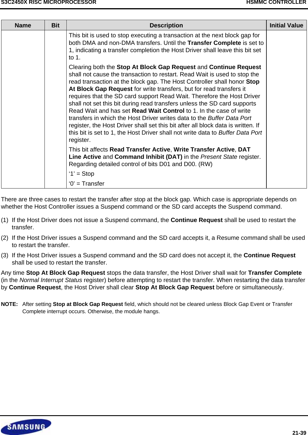
![HSMMC CONTROLLER S3C2450X RISC MICROPROCESSOR 21-40 5.14 WAKEUP CONTROL REGISTER This register is mandatory for the Host Controller, but wakeup functionality depends on the Host Controller system hardware and software. The Host Driver shall maintain voltage on the SD Bus, by setting SD Bus Power to 1 in the Power Control register, when wakeup event via Card Interrupt is desired. Register Address R/W Description Reset ValueWAKCON0 0X4AC0002B R/W Wakeup Control Register (Channel 0) 0x0 WAKCON1 0X4A80002B R/W Wakeup Control Register (Channel 1) 0x0 Name Bit Description Initial Value [7:3] Reserved 0 ENWKUPREM [2] Wakeup Event Enable On SD Card Removal This bit enables wakeup event via Card Removal assertion in the Normal Interrupt Status register. FN_WUS (Wake Up Support) in CIS does not affect this bit. (RW) 1 = Enable 0 = Disable 0 ENWKUPINS [1] Wakeup Event Enable On SD Card Insertion This bit enables wakeup event via Card Insertion assertion in the Normal Interrupt Status register. FN_WUS (Wake Up Support) in CIS does not affect this bit. (RW) 1 = Enable 0 = Disable 0 ENWKUPINT [0] Wakeup Event Enable On Card Interrupt This bit enables wakeup event via Card Interrupt assertion in the Normal Interrupt Status register. This bit can be set to 1 if FN_WUS (Wake Up Support) in CIS is set to 1. (RW) 1 = Enable 0 = Disable 0](https://usermanual.wiki/Diasonic-Technology-Co/RVM-704M.Users-Manual/User-Guide-1826140-Page-538.png)
![S3C2450X RISC MICROPROCESSOR HSMMC CONTROLLER 21-41 5.15 CLOCK CONTROL REGISTER At the initialization of the Host Controller, the Host Driver shall set the SDCLK Frequency Select according to the Capabilities register. Register Address R/W Description Reset ValueCLKCON0 0X4AC0002C R/W Command Register (Channel 0) 0x0 CLKCON1 0X4A80002C R/W Command Register (Channel 1) 0x0 Name Bit Description Initial ValueSELFREQ [15:8] SDCLK Frequency Select This register is used to select the frequency of SDCLK pin. The frequency is not programmed directly; rather this register holds the divisor of the Base Clock Frequency For SD Clock in the Capabilities register. Only the following settings are allowed. 80h base clock divided by 256 40h base clock divided by 128 20h base clock divided by 64 10h base clock divided by 32 08h base clock divided by 16 04h base clock divided by 8 02h base clock divided by 4 01h base clock divided by 2 00h base clock (10MHz-63MHz) Setting 00h specifies the highest frequency of the SD Clock. When setting multiple bits, the most significant bit is used as the divisor. But multiple bits should not be set. The two default divider values can be calculated by the frequency that is defined by the Base Clock Frequency For SD Clock in the Capabilities register. (1) 25MHz divider value (2) 400kHz divider value According to the SD Physical Specification Version 1.01 and the SDIO Card Specification Version 1.0, maximum SD Clock frequency is 25MHz, and shall never exceed this limit. The frequency of SDCLK is set by the following formula: Clock Frequency = (Base Clock) / divisor Thus, choose the smallest possible divisor which results in a clock frequency that is less than or equal to the target frequency. For example, if the Base Clock Frequency For SD Clock in the Capabilities register has the value 33MHz, and the target frequency is 25MHz, then choosing the divisor value of 01h will yield 16.5MHz, which is the nearest frequency less than or equal to the target. Similarly, to approach a clock value of 400kHz, the divisor value of 40h yields the optimal clock value of 258kHz. 0 [7:4] Reserved](https://usermanual.wiki/Diasonic-Technology-Co/RVM-704M.Users-Manual/User-Guide-1826140-Page-539.png)
![HSMMC CONTROLLER S3C2450X RISC MICROPROCESSOR 21-42 Name Bit Description Initial ValueSTBLEXTCLK [3] External Clock Stable This bit is set to 1 when SD Clock output is stable after writing to SD Clock Enable in this register to 1. The SD Host Driver shall wait to issue command to start until this bit is set to 1. (ROC) 1 = Ready 0 = Not Ready 0 ENSDCLK [2] SD Clock Enable The Host Controller shall stop SDCLK when writing this bit to 0. SDCLK Frequency Select can be changed when this bit is 0. Then, the Host Controller shall maintain the same clock frequency until SDCLK is stopped (Stop at SDCLK=0). If the Card Inserted in the Present State register is cleared, this bit shall be cleared. (RW) 1 = Enable 0 = Disable 0 STBLINTCLK [1] Internal Clock Stable This bit is set to 1 when SD Clock is stable after writing to Internal Clock Enable in this register to 1. The SD Host Driver shall wait to set SD Clock Enable until this bit is set to 1. Note: This is useful when using PLL for a clock oscillator that requires setup time. (ROC) 1 = Ready 0 = Not Ready 0 ENINTCLK [0] Internal Clock Enable This bit is set to 0 when the Host Driver is not using the Host Controller or the Host Controller awaits a wakeup interrupt. The Host Controller should stop its internal clock to go very low power state. Still, registers shall be able to be read and written. Clock starts to oscillate when this bit is set to 1. When clock oscillation is stable, the Host Controller shall set Internal Clock Stable in this register to 1. This bit shall not affect card detection. (RW) 1 = Oscillate 0 = Stop](https://usermanual.wiki/Diasonic-Technology-Co/RVM-704M.Users-Manual/User-Guide-1826140-Page-540.png)
![S3C2450X RISC MICROPROCESSOR HSMMC CONTROLLER 21-43 5.16 TIMEOUT CONTROL REGISTER At the initialization of the Host Controller, the Host Driver shall set the Data Timeout Counter Value according to the Capabilities register. Register Address R/W Description Reset ValueTIMEOUTCON 0 0X4AC0002E R/W Timeout Control Register (Channel 0) 0x0 TIMEOUTCON 1 0X4A80002E R/W Timeout Control Register (Channel 1) 0x0 Name Bit Description Initial Value [7:4] Reserved 0 TIMEOUTCON [3:0] Data Timeout Counter Value This value determines the interval by which DAT line timeouts are detected. Refer to the Data Timeout Error in the Error Interrupt Status register for information on factors that dictate timeout generation. Timeout clock frequency will be generated by dividing the base clock SDCLK value by this value. When setting this register, prevent inadvertent timeout events by clearing the Data Timeout Error Status Enable (in the Error Interrupt Status Enable register) 1111b Reserved 1110b SDCLK x 227 1101b SDCLK x 226 ………….. … 0001b SDCLK x 214 0000b SDCLK x 213 0](https://usermanual.wiki/Diasonic-Technology-Co/RVM-704M.Users-Manual/User-Guide-1826140-Page-541.png)
![HSMMC CONTROLLER S3C2450X RISC MICROPROCESSOR 21-44 5.17 SOFTWARE RESET REGISTER A reset pulse is generated when writing 1 to each bit of this register. After completing the reset, the Host Controller shall clear each bit. Because it takes some time to complete software reset, the SD Host Driver shall confirm that these bits are 0. Register Address R/W Description Reset ValueSWRST0 0X4AC0002F R/W Software Reset Register (Channel 0) 0x0 SWRST1 0X4A80002F R/W Software Reset Register (Channel 1) 0x0 Name Bit Description Initial Value [7:3] Reserved 0 RSTDAT [2] Software Reset For DAT Line Only part of data circuit is reset. DMA circuit is also reset. (RWAC) The following registers and bits are cleared by this bit: Present State register Buffer Read Enable Buffer Write Enable Read Transfer Active Write Transfer Active DAT Line Active Command Inhibit (DAT) Block Gap Control register Continue Request Stop At Block Gap Request Normal Interrupt Status register Buffer Read Ready Buffer Write Ready DMA Interrupt Block Gap Event Transfer Complete 1 = Reset 0 = Work 0 RSTCMD [1] Software Reset For CMD Line Only part of command circuit is reset. (RWAC) The following registers and bits are cleared by this bit: Present State register Command Inhibit (CMD) Normal Interrupt Status register Command Complete 1 = Reset 0 = Work 0](https://usermanual.wiki/Diasonic-Technology-Co/RVM-704M.Users-Manual/User-Guide-1826140-Page-542.png)
![S3C2450X RISC MICROPROCESSOR HSMMC CONTROLLER 21-45 Name Bit Description Initial ValueRSTDAT [0] Software Reset For All This reset affects the entire Host Controller except for the card detection circuit. Register bits of type ROC, RW, RW1C, RWAC are cleared to 0. During its initialization, the Host Driver shall set this bit to 1 to reset the Host Controller. The Host Controller shall reset this bit to 0 when capabilities registers are valid and the Host Driver can read them. Additional use of Software Reset For All may not affect the value of the Capabilities registers. If this bit is set to 1, the SD card shall reset itself and must be reinitialized by the Host Driver. (RWAC) 1 = Reset 0 = Work 0](https://usermanual.wiki/Diasonic-Technology-Co/RVM-704M.Users-Manual/User-Guide-1826140-Page-543.png)
![HSMMC CONTROLLER S3C2450X RISC MICROPROCESSOR 21-46 5.18 NORMAL INTERRUPT STATUS REGISTER The Normal Interrupt Status Enable affects reads of this register, but Normal Interrupt Signal Enable does not affect these reads. An interrupt is generated when the Normal Interrupt Signal Enable is enabled and at least one of the status bits is set to 1. For all bits except Card Interrupt and Error Interrupt, writing 1 to a bit clear it; writing to 0 keeps the bit unchanged. More than one status can be cleared with a single register write. The Card Interrupt is cleared when the card stops asserting the interrupt; that is, when the Card Driver services the interrupt condition. Register Address R/W Description Reset ValueNORINTSTS0 0X4AC00030 ROC/RW1C Normal Interrupt Status Register (Channel 0) 0x0 NORINTSTS1 0X4A800030 ROC/RW1C Normal Interrupt Status Register (Channel 1) 0x0 Name Bit Description Initial ValueSTAERR [15] Error Interrupt If any of the bits in the Error Interrupt Status register are set, then this bit is set. Therefore the Host Driver can efficiently test for an error by checking this bit first. This bit is read only. (ROC) 0 = No Error 1 = Error 0 STAFIA3 [14] FIFO SD Address Pointer Interrupt 3 Status (RW1C) 0 = Occurred 1 = Not Occurred 0 STAFIA2 [13] FIFO SD Address Pointer Interrupt 2 Status (RW1C) 0 = Occurred 1 = Not Occurred 0 STAFIA1 [12] FIFO SD Address Pointer Interrupt 1 Status (RW1C) 0 = Occurred 1 = Not Occurred 0 STAFIA0 [11] FIFO SD Address Pointer Interrupt 0 Status (RW1C) 0 = Occurred 1 = Not Occurred 0 STARWAIT [10] Read Wait Interrupt Status (RW1C) 0 = Read Wait Interrupt Occurred 1 = Read Wait Interrupt Not Occurred Note: After checking response for the suspend command, release Read Wait interrupt status manually if BS = 0 0 STACCS [9] CCS Interrupt Status (RW1C) Command Complete Singal Interrupt Status bit is for CE-ATA interface mode. 0 = CCS Interrupt Occurred 1 = CCS Interrupt Not Occurred 0 STACARDINT [8] Card Interrupt Writing this bit to 1 does not clear this bit. It is cleared by resetting the SD card interrupt factor. In 1-bit mode, the Host Controller shall 0](https://usermanual.wiki/Diasonic-Technology-Co/RVM-704M.Users-Manual/User-Guide-1826140-Page-544.png)
![S3C2450X RISC MICROPROCESSOR HSMMC CONTROLLER 21-47 Name Bit Description Initial Valuedetect the Card Interrupt without SD Clock to support wakeup. In 4-bit mode, the card interrupt signal is sampled during the interrupt cycle, so there are some sample delays between the interrupt signal from the SD card and the interrupt to the Host System. It is necessary to define how to handle this delay. When this status has been set and the Host Driver needs to start this interrupt service, Card Interrupt Status Enable in the Normal Interrupt Status Enable register shall be set to 0 in order to clear the card interrupt statuses latched in the Host Controller and to stop driving the interrupt signal to the Host System. After completion of the card interrupt service (It should reset interrupt factors in the SD card and the interrupt signal may not be asserted), set Card Interrupt Status Enable to 1 and start sampling the interrupt signal again. (ROC, RW1C) 1 = Generate Card Interrupt 0 = No Card Interrupt STACARDREM [7] Card Removal This status is set if the Card Inserted in the Present State register changes from 1 to 0. When the Host Driver writes this bit to 1 to clear this status, the status of the Card Inserted in the Present State register should be confirmed. Because the card detect state may possibly be changed when the Host Driver clear this bit and interrupt event may not be generated. (RW1C) 1 = Card removed 0 = Card state stable or Debouncing 0 STACARDINS [6] Card Insertion This status is set if the Card Inserted in the Present State register changes from 0 to 1. When the Host Driver writes this bit to 1 to clear this status, the status of the Card Inserted in the Present State register should be confirmed. Because the card detect state may possibly be changed when the Host Driver clear this bit and interrupt event may not be generated. (RW1C) 1 = Card inserted 0 = Card state stable or Debouncing 0 STABUFRDRDY [5] Buffer Read Ready This status is set if the Buffer Read Enable changes from 0 to 1. Refer to the Buffer Read Enable in the Present State register. (RW1C) 1 = Ready to read buffer 0 = Not ready to read buffer 0 STABUFWTRDY [4] Buffer Write Ready This status is set if the Buffer Write Enable changes from 0 to 1. Refer to the Buffer Write Enable in the Present State register. (RW1C) 1 = Ready to write buffer 0 = Not ready to write buffer 0](https://usermanual.wiki/Diasonic-Technology-Co/RVM-704M.Users-Manual/User-Guide-1826140-Page-545.png)
![HSMMC CONTROLLER S3C2450X RISC MICROPROCESSOR 21-48 Name Bit Description Initial ValueSTADMAINT [3] DMA Interrupt This status is set if the Host Controller detects the Host DMA Buffer boundary during transfer. Refer to the Host DMA Buffer Boundary in the Block Size register. Other DMA interrupt factors may be added in the future. This interrupt shall not be generated after the Transfer Complete. (RW1C) 1 = DMA Interrupt is generated 0 = No DMA Interrupt 0 STABLKGAP [2] Block Gap Event If the Stop At Block Gap Request in the Block Gap Control register is set, this bit is set when both a read / write transaction is stopped at a block gap. If Stop At Block Gap Request is not set to 1, this bit is not set to 1. (1) In the case of a Read Transaction This bit is set at the falling edge of the DAT Line Active Status (When the transaction is stopped at SD Bus timing. The Read Wait must be supported in order to use this function. (2) Case of Write Transaction This bit is set at the falling edge of Write Transfer Active Status (After getting CRC status at SD Bus timing). 1 = Transaction stopped at block gap 0 = No Block Gap Event 0 STATRANCMPLT [1] Transfer Complete This bit is set when a read / write transfer is completed. (1) In the case of a Read Transaction This bit is set at the falling edge of Read Transfer Active Status. There are two cases in which this interrupt is generated. The first is when a data transfer is completed as specified by data length (After the last data has been read to the Host System). The second is when data has stopped at the block gap and completed the data transfer by setting the Stop At Block Gap Request in the Block Gap Control register (After valid data has been read to the Host System). (2) In the case of a Write Transaction This bit is set at the falling edge of the DAT Line Active Status. There are two cases in which this interrupt is generated. The first is when the last data is written to the SD card as specified by data length and the busy signal released. The second is when data transfers are stopped at the block gap by setting Stop At Block Gap Request in the Block Gap Control register and data transfers completed. (After valid data is written to the SD card and the busy signal released). (RW1C) The table below shows that Transfer Complete has higher priority 0](https://usermanual.wiki/Diasonic-Technology-Co/RVM-704M.Users-Manual/User-Guide-1826140-Page-546.png)
![S3C2450X RISC MICROPROCESSOR HSMMC CONTROLLER 21-49 Name Bit Description Initial Valuethan Data Timeout Error. If both bits are set to 1, the data transfer can be considered complete. Relation between Transfer Complete and Data Transfer Complete Data Timeout Error Meaning of the status 0 0 Interrupted by another factor 0 1 Timeout occur during transfer 1 Don’t care Data transfer complete 1 = Data Transfer Complete 0 = No transfer complete STACMDCMPLT [0] Command Complete This bit is set when get the end bit of the command response. (Except Auto CMD12) Refer to Command Inhibit (CMD) in the Present State register. The table below shows that Command Timeout Error has higher priority than Command Complete. If both bits are set to 1, it can be considered that the response was not received correctly. Command Complete Command Timeout Error Meaning of the status 0 0 Interrupted by another factor Don’t care 1 Response not received within 64 SDCLK cycles. 1 0 Response received 1 = Command Complete 0 = No command complete 0 NOTES: 1. Host Driver may check if interrupt is actually cleared by polling or monitoring the INTREQ port. If HCLK is much faster than SDCLK, it takes long time to be cleared for the bits actually. 2. Card Interrupt status bit keeps previous value until next card interrupt period (level interrupt) and can be cleared when write to 1 (RW1C).](https://usermanual.wiki/Diasonic-Technology-Co/RVM-704M.Users-Manual/User-Guide-1826140-Page-547.png)
![HSMMC CONTROLLER S3C2450X RISC MICROPROCESSOR 21-50 5.19 ERROR INTERRUPT STATUS REGISTER Signals defined in this register can be enabled by the Error Interrupt Status Enable register, but not by the Error Interrupt Signal Enable register. The interrupt is generated when the Error Interrupt Signal Enable is enabled and at least one of the statuses is set to 1. Writing to 1 clears the bit and writing to 0 keeps the bit unchanged. More than one status can be cleared at the one register write. Register Address R/W Description Reset ValueERRINTSTS0 0X4AC00032 ROC/RW1C Error Interrupt Status Register (Channel 0) 0x0 ERRINTSTS1 0X4A800032 ROC/RW1C Error Interrupt Status Register (Channel 1) 0x0 Name Bit Description Initial Value [15:10] Reserved 0 ADMAERR [9] ADMA Error This bit is set when the Host Controller detects errors during ADMA based data transfer. The state of the ADMA at an error occurrence is saved in the ADMA Error Status Register, In addition, the Host Controller generates this Interrupt when it detects invalid descriptor data (Valid=0) at the ST_FDS state. ADMA Error State in the ADMA Error Status indicates that an error occurs in ST_FDS state. The Host Driver may find that Valid bit is not set at the error descriptor. 1 = Error 0 = No Error 0 STAACMDERR [8] Auto CMD12 Error Occurs when detecting that one of the bits in Auto CMD12 Error Status register has changed from 0 to 1. This bit is set to 1,not only when the errors in Auto CMD12 occur but also when Auto CMD12 is not executed due to the previous command error. 1 = Error 0 = No Error 0 STACURERR [7] Current Limit Error Not implemented in this version. Always 0. 0 STADENDERR [6] Data End Bit Error Occurs either when detecting 0 at the end bit position of read data which uses the DAT line or at the end bit position of the CRC Status. 1 = Error 0 = No Error 0 STADATCRCERR [5] Data CRC Error Occurs when detecting CRC error when transferring read data which uses the DAT line or when detecting the Write CRC status having a value of other than "010". 1 = Error 0 = No Error 0 STADATTOUTERR [4] Data Timeout Error 0](https://usermanual.wiki/Diasonic-Technology-Co/RVM-704M.Users-Manual/User-Guide-1826140-Page-548.png)
![S3C2450X RISC MICROPROCESSOR HSMMC CONTROLLER 21-51 Name Bit Description Initial ValueOccurs when detecting one of following timeout conditions. (1) Busy timeout for R1b,R5b type (2) Busy timeout after Write CRC status (3) Write CRC Status timeout (4) Read Data timeout. 1 = Timeout 0 = No Error STACMDIDXERR [3] Command Index Error Occurs if a Command Index error occurs in the command response. 1 = Error 0 = No Error 0 CMDEBITERR [2] Command End Bit Error Occurs when detecting that the end bit of a command response is 0. 1 = End bit Error generated 0 = No Error STACMDCRCERR [1] Command CRC Error Command CRC Error is generated in two cases. (1) If a response is returned and the Command Timeout Error is set to 0 (indicating no timeout), this bit is set to 1 when detecting a CRC error in the command response. (2) The Host Controller detects a CMD line conflict by monitoring the CMD line when a command is issued. If the Host Controller drives the CMD line to 1 level, but detects 0 level on the CMD line at the next SDCLK edge, then the Host Controller shall abort the command (Stop driving CMD line) and set this bit to 1. The Command Timeout Error shall also be set to 1 to distinguish CMD line conflict. 1 = CRC Error generated 0 = No Error 0 STACMDTOUTERR [0] Command Timeout Error Occurs only if no response is returned within 64 SDCLK cycles from the end bit of the command. If the Host Controller detects a CMD line conflict, in which case Command CRC Error shall also be set as shown in Table 33, this bit shall be set without waiting for 64 SDCLK cycles because the command will be aborted by the Host Controller. 1 = Timeout 0 = No Error 0](https://usermanual.wiki/Diasonic-Technology-Co/RVM-704M.Users-Manual/User-Guide-1826140-Page-549.png)
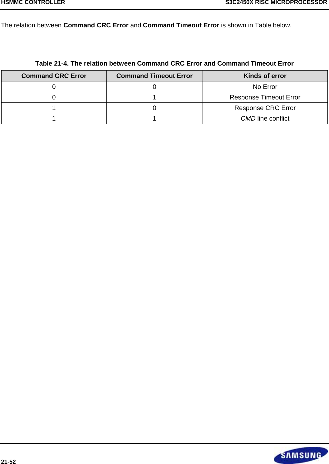
![S3C2450X RISC MICROPROCESSOR HSMMC CONTROLLER 21-53 5.20 NORMAL INTERRUPT STATUS ENABLE REGISTER Setting to 1 enables Interrupt Status. Register Address R/W Description Reset ValueNORINTSTSEN0 0X4AC00034 R/W Normal Interrupt Status Enable Register (Channel 0) 0x0 NORINTSTSEN1 0X4A800034 R/W Normal Interrupt Status Enable Register (Channel 1) 0x0 Name Bit Description Initial Value [15] Fixed to 0 The Host Driver shall control error interrupts using the Error Interrupt Status Enable register. (RO) 0 ENSTAFIA3 [14] FIFO SD Address Pointer Interrupt 3 Status Enable 1 = Enabled 0 = Masked 0 ENSTAFIA2 [13] FIFO SD Address Pointer Interrupt 2 Status Enable 1 = Enabled 0 = Masked 0 ENSTAFIA1 [12] FIFO SD Address Pointer Interrupt 1 Status Enable 1 = Enabled 0 = Masked 0 ENSTAFIA0 [11] FIFO SD Address Pointer Interrupt 0 Status Enable 1 = Enabled 0 = Masked 0 ENSTARWAIT [10] Read Wait interrupt status enable 1 = Enabled 0 = Masked 0 ENSTACCS [9] CCS Interrupt Status Enable 1 = Enabled 0 = Masked 0 ENSTACARDINT [8] Card Interrupt Status Enable If this bit is set to 0, the Host Controller shall clear interrupt request to the System. The Card Interrupt detection is stopped when this bit is cleared and restarted when this bit is set to 1. The Host Driver should clear the Card Interrupt Status Enable before servicing the Card Interrupt and should set this bit again after all interrupt requests from the card are cleared to prevent inadvertent interrupts. 1 = Enabled 0 = Masked 0 ENSTACARDREM [7] Card Removal Status Enable 1 = Enabled 0 = Masked 0](https://usermanual.wiki/Diasonic-Technology-Co/RVM-704M.Users-Manual/User-Guide-1826140-Page-551.png)
![HSMMC CONTROLLER S3C2450X RISC MICROPROCESSOR 21-54 Name Bit Description Initial ValueENSTACARDNS [6] Card Insertion Status Enable 1 = Enabled 0 = Masked 0 ENSTABUFRDRDY [5] Buffer Read Ready Status Enable 1 = Enabled 0 = Masked 0 ENSTABUFWTRDY [4] Buffer Write Ready Status Enable 1 = Enabled 0 = Masked 0 ENSTADMA [3] DMA Interrupt Status Enable 1 = Enabled 0 = Masked 0 ENSTABLKGAP [2] Block Gap Event Status Enable 1 = Enabled 0 = Masked 0 ENSTASTANSCMPLT [1] Transfer Complete Status Enable 1 = Enabled 0 = Masked 0 ENSTACMDCMPLT [0] Command Complete Status Enable 1 = Enabled 0 = Masked 0](https://usermanual.wiki/Diasonic-Technology-Co/RVM-704M.Users-Manual/User-Guide-1826140-Page-552.png)
![S3C2450X RISC MICROPROCESSOR HSMMC CONTROLLER 21-55 5.21 ERROR INTERRUPT STATUS ENABLE REGISTER Setting to 1 enables Error Interrupt Status. Register Address R/W Description Reset ValueERRINTSTSEN0 0X4AC00036 R/W Error Interrupt Status Enable Register (Channel 0) 0x0 ERRINTSTSEN1 0X4A800036 R/W Error Interrupt Status Enable Register (Channel 1) 0x0 Name Bit Description Initial Value [15:10] Reserved 0 ADMAERR [9] ADMA Error Status Enable 1 = Enabled 0 = Masked 0 ENSTAACMDERR [8] Auto CMD12 Error Status Enable 1 = Enabled 0 = Masked 0 ENSTACURERR [7] Current Limit Error Status Enable This function is not implemented in this version. 1 = Enabled 0 = Masked 0 ENSTADENDERR [6] Data End Bit Error Status Enable 1 = Enabled 0 = Masked 0 ENSTADATCRCERR [5] Data CRC Error Status Enable 1 = Enabled 0 = Masked 0 ENSTADATTOUTERR [4] Data Timeout Error Status Enable 1 = Enabled 0 = Masked 0 ENSTACMDIDXERR [3] Command Index Error Status Enable 1 = Enabled 0 = Masked 0 ENSTACMDEBITERR [2] Command End Bit Error Status Enable 1 = Enabled 0 = Masked 0 ENSTACMDCRCERR [1] Command CRC Error Status Enable 1 = Enabled 0 = Masked 0 ENSTACMDTOUTERR [0] Command Timeout Error Status Enable 1 = Enabled 0 = Masked 0](https://usermanual.wiki/Diasonic-Technology-Co/RVM-704M.Users-Manual/User-Guide-1826140-Page-553.png)
![HSMMC CONTROLLER S3C2450X RISC MICROPROCESSOR 21-56 5.22 NORMAL INTERRUPT SIGNAL ENABLE REGISTER This register is used to select which interrupt status is indicated to the Host System as the interrupt. These status bits all share the same1 bit interrupt line. Setting any of these bits to 1 enables interrupt generation. Register Address R/W Description Reset ValueNORINTSIGEN0 0X4AC00038 R/W Normal Interrupt Signal Enable Register (Channel 0) 0x0 NORINTSIGEN1 0X4A800038 R/W Normal Interrupt Signal Enable Register (Channel 1) 0x0 Name Bit Description Initial Value [15] Fixed to 0 The Host Driver shall control error interrupts using the Error Interrupt Signal Enable register. 0 ENSIGFIA3 [14] FIFO SD Address Pointer Interrupt 3 Signal Enable 1 = Enabled 0 = Masked 0 ENSIGFIA2 [13] FIFO SD Address Pointer Interrupt 2 Signal Enable 1 = Enabled 0 = Masked 0 ENSIGFIA1 [12] FIFO SD Address Pointer Interrupt 1 Signal Enable 1 = Enabled 0 = Masked 0 ENSIGFIA0 [11] FIFO SD Address Pointer Interrupt 0 Signal Enable 1 = Enabled 0 = Masked 0 ENSIGRWAIT [10] Read Wait Interrupt Signal Enable 1 = Enabled 0 = Masked 0 ENSIGCCS [9] CCS Interrupt Signal Enable Command Complete Signal Interrupt Status bit is for CE-ATA interface mode. 1 = Enabled 0 = Masked 0 ENSIGCARDINT [8] Card Interrupt Signal Enable 1 = Enabled 0 = Masked 0 ENSIGCARDREM [7] Card Removal Signal Enable 1 = Enabled 0 = Masked 0 ENSIGCARDNS [6] Card Insertion Signal Enable 1 = Enabled 0 = Masked 0](https://usermanual.wiki/Diasonic-Technology-Co/RVM-704M.Users-Manual/User-Guide-1826140-Page-554.png)
![S3C2450X RISC MICROPROCESSOR HSMMC CONTROLLER 21-57 Name Bit Description Initial ValueENSIGBUFRDRDY [5] Buffer Read Ready Signal Enable 1 = Enabled 0 = Masked 0 ENSIGBUFWTRDY [4] Buffer Write Ready Signal Enable 1 = Enabled 0 = Masked 0 ENSIGDMA [3] DMA Interrupt Signal Enable 1 = Enabled 0 = Masked 0 ENSIGBLKGAP [2] Block Gap Event Signal Enable 1 = Enabled 0 = Masked 0 ENSIGSTANSCMPLT [1] Transfer Complete Signal Enable 1 = Enabled 0 = Masked 0 ENSIGCMDCMPLT [0] Command Complete Signal Enable 1 = Enabled 0 = Masked 0](https://usermanual.wiki/Diasonic-Technology-Co/RVM-704M.Users-Manual/User-Guide-1826140-Page-555.png)
![HSMMC CONTROLLER S3C2450X RISC MICROPROCESSOR 21-58 5.23 ERROR INTERRUPT SIGNAL ENABLE REGISTER This register is used to select which interrupt status is notified to the Host System as the interrupt. These status bits all share the same 1 bit interrupt line. Setting any of these bits to 1 enables interrupt generation. Register Address R/W Description Reset ValueERRINTSIGEN0 0X4AC0003A R/W Error Interrupt Signal Enable Register (Channel 0) 0x0 ERRINTSIGEN1 0X4A80003A R/W Error Interrupt Signal Enable Register (Channel 1) 0x0 Name Bit Description Initial Value [15:10] Reserved 0 ENSIGADMAERR [9] ADMA Error Signal Enable 1 = Enabled 0 = Masked 0 ENSIGACMDERR [8] Auto CMD12 Error Signal Enable 1 = Enabled 0 = Masked 0 ENSIGCURERR [7] Current Limit Error Signal Enable This function is not implemented in this version. 1 = Enabled 0 = Masked 0 ENSIGDENDERR [6] Data End Bit Error Signal Enable 1 = Enabled 0 = Masked 0 ENSIGDATCRCERR [5] Data CRC Error Signal Enable 1 = Enabled 0 = Masked 0 ENSIGDATTOUTERR [4] Data Timeout Error Signal Enable 1 = Enabled 0 = Masked 0 ENSIGCMDIDXERR [3] Command Index Error Signal Enable 1 = Enabled 0 = Masked 0 ENSIGCMDEBITERR [2] Command End Bit Error Signal Enable 1 = Enabled 0 = Masked 0 ENSIGCMDCRCERR [1] Command CRC Error Signal Enable 1 = Enabled 0 = Masked 0 ENSIGCMDTOUTERR [0] Command Timeout Error Signal Enable 1 = Enabled 0 = Masked 0 Detailed documents are to be copied from SD Host Standard Spec.](https://usermanual.wiki/Diasonic-Technology-Co/RVM-704M.Users-Manual/User-Guide-1826140-Page-556.png)
![S3C2450X RISC MICROPROCESSOR HSMMC CONTROLLER 21-59 5.24 AUTOCMD12 ERROR STATUS REGISTER When Auto CMD12 Error Status is set, the Host Driver shall check this register to identify what kind of error Auto CMD12 indicated. This register is valid only when the Auto CMD12 Error is set. Register Address R/W Description Reset ValueACMD12ERRSTS0 0X4AC0003C ROC Auto CMD12 Error Status Register (Channel 0) 0x0 ACMD12ERRSTS1 0X4A80003C ROC Auto CMD12 Error Status Register (Channel 1) 0x0 Name Bit Description Initial Value [15:8] Reserved 0 STANCMDAER [7] Command Not Issued By Auto CMD12 Error Setting this bit to 1 means CMD_wo_DAT is not executed due to an Auto CMD12 Error (D04-D01) in this register. 1 = Not Issued 0 = No error 0 [6:5] Reserved 0 STACMDIDXERR [4] Auto CMD12 Index Error Occurs if the Command Index error occurs in response to a command. 1 = Error 0 = No Error 0 STACMDEBITAER [3] Auto CMD12 End Bit Error Occurs when detecting that the end bit of command response is 0. 1 = End Bit Error Generated 0 = No Error 0 STACMDCRCAER [2] Auto CMD12 CRC Error Occurs when detecting a CRC error in the command response. 1 = CRC Error Generated 0 = No Error 0 STACMDTOUTAER [1] Auto CMD12 Timeout Error Occurs if no response is returned within 64 SDCLK cycles from the end bit of command. If this bit is set to1, the other error status bits (D04-D02) are meaningless. 1 = Time out 0 = No Error 0 STANACMDAER [0] Auto CMD12 Not Executed If memory multiple block data transfer is not started due to command error, this bit is not set because it is not necessary to issue Auto CMD12. Setting this bit to 1 means the Host Controller cannot issue Auto CMD12 to stop memory multiple block data transfer due to some error. If this bit is set to 1, other error status bits (D04-D01) are meaningless. 1 = Not executed 0 = Executed 0](https://usermanual.wiki/Diasonic-Technology-Co/RVM-704M.Users-Manual/User-Guide-1826140-Page-557.png)
![S3C2450X RISC MICROPROCESSOR HSMMC CONTROLLER 21-61 5.25 CAPABILITIES REGISTER This register provides the Host Driver with information specific to the Host Controller implementation. The Host Controller may implement these values as fixed or loaded from flash memory during power on initialization. Refer to Software Reset for All in the Software Reset register for loading from flash memory and completion timing control. Register Address R/W Description Reset ValueCAPAREG0 0X4AC00040 HWInit Capabilities Register (Channel 0) 0x05E80080CAPAREG1 0X4A800040 HWInit Capabilities Register (Channel 1) 0x05E80080 Name Bit Description Initial Value [31:27] Reserved CAPAV18 [26] Voltage Support 1.8V (HWInit) 1 = 1.8V Supported 0 = 1.8V Not Supported 1 CAPAV30 [25] Voltage Support 3.0V (HWInit) 1 = 3.0V Supported 0 = 3.0V Not Supported 0 CAPAV33 [24] Voltage Support 3.3V (HWInit) 1 = 3.3V Supported 0 = 3.3V Not Supported 1 CAPASUSRES [23] Suspend/Resume Support (HWInit) This bit indicates whether the Host Controller supports Suspend / Resume functionality. If this bit is 0, the Suspend and Resume mechanism are not supported and the Host Driver shall not issue either Suspend or Resume commands. 1 = Supported 0 = Not Supported 1 CAPADMA [22] DMA Support (HWInit) This bit indicates whether the Host Controller is capable of using DMA to transfer data between system memory and the Host Controller directly. 1 = DMA Supported 0 = DMA Not Supported 1 CAPAHSPD [21] High Speed Support (HWInit) This bit indicates whether the Host Controller and the Host System support High Speed mode and they can supply SD Clock frequency from 25MHz to 50MHz. 1 = High Speed Supported 0 = High Speed Not Supported 1 [20:18] Reserved](https://usermanual.wiki/Diasonic-Technology-Co/RVM-704M.Users-Manual/User-Guide-1826140-Page-559.png)
![HSMMC CONTROLLER S3C2450X RISC MICROPROCESSOR 21-62 Name Bit Description Initial ValueCAPAMAXBLKLEN [17:16] Max Block Length (HWInit) This value indicates the maximum block size that the Host Driver can read and write to the buffer in the Host Controller. The buffer shall transfer this block size without wait cycles. Three sizes can be defined as indicated below. 00 = 512-byte 01 = 1024-byte 10 = 2048-byte 11 = Reserved 0 [15:14] Reserved 0 CAPABASECLK [13:8] Base Clock Frequency For SD Clock (HWInit) This value indicates the base (maximum) clock frequency for the SD Clock. Unit values are 1MHz. If the real frequency is 16.5MHz, the lager value shall be set 01 0001b (17MHz) because the Host Driver use this value to calculate the clock divider value (Refer to the SDCLK Frequency Select in the Clock Control register.) and it shall not exceed upper limit of the SD Clock frequency. The supported clock range is 10MHz to 63MHz. If these bits are all 0, the Host System has to get information via another method. Not 0 = 1MHz to 63MHz 000000b = Get information via another method 0 CAPATOUTUNIT [7] Timeout Clock Unit (HWInit) This bit shows the unit of base clock frequency used to detect Data Timeout Error. 0 = kHz 1 = MHz 1 [6] Reserved 0 CAPATOUTCLK [5:0] Timeout Clock Frequency (HWInit) This bit shows the base clock frequency used to detect Data Timeout Error. The Timeout Clock Unit defines the unit of this field value. Timeout Clock Unit =0 [kHz] unit: 1kHz to 63kHz Timeout Clock Unit =1 [MHz] unit: 1MHz to 63MHz Not 0 = 1kHz to 63kHz or 1MHz to 63MHz 00 0000b = Get information via another method 0](https://usermanual.wiki/Diasonic-Technology-Co/RVM-704M.Users-Manual/User-Guide-1826140-Page-560.png)
![S3C2450X RISC MICROPROCESSOR HSMMC CONTROLLER 21-63 5.26 MAXIMUM CURRENT CAPABILITIES REGISTER These registers indicate maximum current capability for each voltage. The value is meaningful if Voltage Support is set in the Capabilities register. If this information is supplied by the Host System via another method, all Maximum Current Capabilities register shall be 0. Register Address R/W Description Reset ValueMAXCURR0 0X4AC00048 HWInit Maximum Current Capabilities Register (Channel 0) 0x0 MAXCURR1 0X4A800048 HWInit Maximum Current Capabilities Register (Channel 1) 0x0 Name Bit Description Initial Value [31:24] Reserved MAXCURR18 [23:16] Maximum Current for 1.8V (HWInit) 0 MAXCURR30 [15:8] Maximum Current for 3.0V (HWInit) 0 MAXCURR33 [7:0] Maximum Current for 3.3V (HWInit) 0 This register measures current in 4mA steps. Each voltage level’s current support is described using the Table below. Table 21-6. Maximum Current Value Definition Register Value Current Value 0 Get information via another method 1 4mA 2 8mA 3 12mA … … 255 1020mA](https://usermanual.wiki/Diasonic-Technology-Co/RVM-704M.Users-Manual/User-Guide-1826140-Page-561.png)
![HSMMC CONTROLLER S3C2450X RISC MICROPROCESSOR 21-64 5.27 CONTROL REGISTER 2 Register Address R/W Description Reset ValueCONTROL2_0 0X4AC00080 R/W Control register 2 (Channel 0) 0x0 CONTROL2_1 0X4A800080 R/W Control register 2 (Channel 1) 0x0 Name Bit Description Initial Value [31] Write Status Clear Async Mode Enable This bit can make async-clear enable about Normal and Error interrupt status bit. During the initialization procedure command operation, this bit should be enabled. 0 = Disable 1 = Enable 0 CDINVRXD3 [30] Command Conflict Mask Enable This bit can mask enable the Command Conflict Status (bit [1:0] of the “ERROR INTERRUPT STATUS REGISTER”) 0 = Mask Disable 1 = Mask Enable 0 CDINVRXD3 [29] Card Detect signal inversion for RX_DAT[3] 0 = Disable 1 = Enable 0 SELCARDOUT [28] Card Removed Condition Selection 0 = Card Removed condition is “Not Card Insert” State (When the transition from “Card Inserted” state to “Debouncing” state) 1 = Card Removed state is “Card Out” State (When the transition from “Debouncing state to “No Card” state) 0 FLTCLKSEL [27:24] Filter Clock (iFLTCLK) Selection Filter Clock period = 2^(FltClkSel + 5) x iSDCLK period 0000 = 25 x iSDCLK, 0001 = 26 x iSDCLK … 1111 = 220 x iSDCLK 0 LVLDAT [23:16] DAT line level Bit[23]=DAT[7], BIT[22]=DAT[6], BIT[21]=DAT[5], BIT[20]=DAT[4], Bit[19]=DAT[3], BIT[18]=DAT[2], BIT[17]=DAT[1], BIT[16]=DAT[0] (Read Only) Line state ENFBCLKTX [15] Feedback Clock Enable for Tx Data/Command Clock 0 = Disable 1 = Enable 0 ENFBCLKRX [14] Feedback Clock Enable for Rx Data/Command Clock 0 = Disable 1 = Enable 0 SDCDSEL [13] SD Card Detect Signal Selection 0](https://usermanual.wiki/Diasonic-Technology-Co/RVM-704M.Users-Manual/User-Guide-1826140-Page-562.png)
![S3C2450X RISC MICROPROCESSOR HSMMC CONTROLLER 21-65 Name Bit Description Initial ValueCard Detect Pin Level does not simply reflect SDCD# pin, but chooses from SDCD, DAT[3], or CDTestlvl depending on CDSigSel and this field (SDCDSel) values 0 = nSDCD is used for SD Card Detect Signal 1 = DAT[3] is used for SD Card Detect Signal CDSYNCSEL [12] SD Card Detect Sync Support This field is used to enable output CMD and DAT referencing SD Bus Power bit in the “PWRCON register”, when being set. 0 = No Sync, no switch output enable signal (Command, Data) 1 = Sync, control output enable signal (Command, Data) 0 ENBUSYCHKTXSTART [11] CE-ATA I/F mode Busy state check before Tx Data start state 0 = Disable 1 = Enable 0 DFCNT [10:9] Debounce Filter Count Debounce Filter Count setting register for Card Detect signal input (SDCD#) 00 = No use debounce filter 01 = 4 iSDCLK 10 = 16 iSDCLK 11 = 64 iSDCLK 0 ENCLKOUTHOLD [8] SDCLK Hold Enable The enter and exit of the SDCLK Hold state is done by Host Controller. 0 = Disable 1 = Enable 0 RWAITMODE [7] Read Wait Release Control 0 = Read Wait state is released by the Host Controller (Auto) 1 = Read Wait state is released by the Host Device (Manual) 0 DISBUFRD [6] Buffer Read Disable 0 = Normal mode, user can read buffer(FIFO) data using 0x20 register 1 = User cannot read buffer (FIFO) data using 0x20 register. In this case, the buffer memory only can be read through memory area. (Debug purpose) 0 SELBASECLK [5:4] Base Clock Source Select 00 or 01 = HCLK 10 = SCLK_HSMMC# : EPLLout, MPLLout, PLL_source_clk or CLK27 clock (from SYSCON block, can be selected by MMC#_SEL[1:0] fields of the CLK_SRC register in SYSCON block) 11 = External Clock source (XTI or XEXTCLK) 00](https://usermanual.wiki/Diasonic-Technology-Co/RVM-704M.Users-Manual/User-Guide-1826140-Page-563.png)
![HSMMC CONTROLLER S3C2450X RISC MICROPROCESSOR 21-66 Name Bit Description Initial ValuePWRSYNC [3] SD OP Power Sync Support with SD Card This field is used to enable input CMD and DAT referencing SD Bus Power bit in the “PWRCON register”, when being set. 0 = No Sync, no switch input enable signal (Command, Data) 1 = Sync, control input enable signal (Command, Data) 0 [2] Reserved 0 ENCLKOUTMSKCON [1] SDCLK output clock masking when Card Insert cleared This field when High is used not to stop SDCLK when No Card state. 0 = Disable 1 = Enable 0 HWINITFIN [0] SD Host Controller Hardware Initialization Finish 0 = Not Finish 1 = Finish 0 NOTES: 1. Ensure to always set SDCLK Hold Enable (EnSCHold) if the card does not support Read Wait to guarantee for Receive data not overwritten to the internal FIFO memory. 2. CMD_wo_DAT issue is prohibited during READ transfer when SDCLK Hold Enable is set](https://usermanual.wiki/Diasonic-Technology-Co/RVM-704M.Users-Manual/User-Guide-1826140-Page-564.png)
![S3C2450X RISC MICROPROCESSOR HSMMC CONTROLLER 21-67 5.28 CONTROL REGISTER 3 Register Address R/W Description Reset ValueCONTROL3_0 0X4AC00084 R/W FIFO Interrupt Control (Control Register 3) (Channel 0) 0x7F5F3F1FCONTROL3_1 0X4A800084 R/W FIFO Interrupt Control (Control Register 3) (Channel 1) 0x7F5F3F1F Name Bit Description Initial ValueFCSEL3 [31] Feedback Clock Select [3] Reference (note 1) 0x0 FIA3 [30:24] FIFO Interrupt Address register 3 FIFO (512Byte Buffer memory, word address unit) Initial value (0x7F) generates at 512-byte (128-word) position. 0x7F FCSEL2 [23] Feedback Clock Select [2] Reference (note 1) 0x0 FIA2 [22:16] FIFO Interrupt Address register 2 FIFO (512Byte Buffer memory, word address unit) Initial value (0x5F) generates at 384-byte (96-word) position. 0x5F FCSEL1 [15] Feedback Clock Select [1] Reference (note 2) 0x0 FIA1 [14:8] FIFO Interrupt Address register 1 FIFO (512Byte Buffer memory, word address unit) Initial value (0x3F) generates at 256-byte (64-word) position. 0x3F FCSEL0 [7] Feedback Clock Select [0] Reference (note 2) 0x0 FIA0 [6:0] FIFO Interrupt Address register 0 FIFO (512Byte Buffer memory, word address unit) Initial value (0x1F) generates at 128-byte (32-word) position. 0x1F NOTES: 1. FCSel[3:2] : Tx Feedback Clock Delay Control : Inverter delay means 10ns delay when SDCLK 50MHz setting 01 = Delay1 (basic delay), 11 = Delay2 (basic delay + 2ns), 00 = Delay3 (inverter delay), 10 = Delay4 (inverter delay + 2ns) 2. FCSel[1:0] : Rx Feedback Clock Delay Control : Inverter delay means10ns delay when SDCLK 50MHz setting 01 = Delay1 (basic delay), 11 = Delay2 (basic delay + 2ns), 00 = Delay3 (inverter delay), 10 = Delay4 (inverter delay + 2ns) 3. Tx Feedback inversion setting (FCSel[3:2] = 00 or 10), Tx Feedback clock enable (ENFBCLKTX=0) and Normal Speed mode (ENHIGHSPD = 0) setting make Tx data transfer mismatch (Do not set).](https://usermanual.wiki/Diasonic-Technology-Co/RVM-704M.Users-Manual/User-Guide-1826140-Page-565.png)
![HSMMC CONTROLLER S3C2450X RISC MICROPROCESSOR 21-68 5.29 DEBUG REGISTER Register Address R/W Description Reset ValueDEBUG_0 0X4AC00088 R/W DEBUG register (Channel 0) Not fixed DEBUG_1 0X4A800088 R/W DEBUG register (Channel 1) Not fixed Name Bit Description Initial ValueDBGREG [31:0] Debug Register Read Only Register for Debug Purpose (RO) Not fixed 5.30 CONTROL REGISTER 4 Register Address R/W Description Reset ValueCONTROL4_0 0x4AC0008C R/W Control register 4 (Channel 0) 0x0 CONTROL4_1 0x4A80008C R/W Control register 4 (Channel 1) 0x0 Name Bit Description Initial ValueReserved [31:1] − 0 StaBusy [0] Status Busy This bit is “High” when the clock domain crossing (HCLK to SDCLK) operation is processing. This bit is status bit and Read Only (RO) 0](https://usermanual.wiki/Diasonic-Technology-Co/RVM-704M.Users-Manual/User-Guide-1826140-Page-566.png)
![S3C2450X RISC MICROPROCESSOR HSMMC CONTROLLER 21-69 5.31 FORCE EVENT REGISTER FOR AUTO CMD12 ERROR STATUS Register Address R/W Description Reset ValueFEAER0 0X4AC00050 WO Force Event Auto CMD12 Error Interrupt Register Error Interrupt (Channel 0) 0x0000 FEAER1 0X4A800050 WO Force Event Auto CMD12 Error Interrupt Register Error Interrupt (Channel 1) 0x0000 The Force Event Register is not a physically implemented register. Rather, it is an address at which the Auto CMD12 Error Status Register can be written. • Writing 1: set each bit of the Auto CMD12 Error Status Register • Writing 0: no effect D15 D12 Name Bit Description Initial Value [15:8] − 0x0 [7] Force Event for Command Not Issued By Auto CMD12 Error 1 = Interrupt is generated 0 = No Interrupt 0 [6:5] − 0 [4] Force Event for Auto CMD12 Index Error 1 = Interrupt is generated 0 = No Interrupt 0 [3] Force Event for Auto CMD12 End Bit Error 1 = Interrupt is generated 0 = No Interrupt 0 [2] Force Event for Auto CMD12 CRC Error 1 = Interrupt is generated 0 = No Interrupt 0 [1] Force Event for Auto CMD12 Timeout Error 1 = Interrupt is generated 0 = No Interrupt 0 [0] Force Event for Auto CMD12 Not Executed 1 = Interrupt is generated 0 = No Interrupt 0](https://usermanual.wiki/Diasonic-Technology-Co/RVM-704M.Users-Manual/User-Guide-1826140-Page-567.png)
![HSMMC CONTROLLER S3C2450X RISC MICROPROCESSOR 21-70 5.32 FORCE EVENT REGISTER FOR ERROR INTERRUPT STATUS Register Address R/W Description Reset ValueFEERR0 0X4AC00052 WO Force Event Error Interrupt Register Error Interrupt (Channel 0) 0x0000 FEERR1 0X4A800052 WO Force Event Error Interrupt Register Error Interrupt (Channel 1) 0x0000 The Force Event Register is not a physically implemented register. Rather, it is an address at which the Error Interrupt Status register can be written. The effect of a write to this address will be reflected in the Error Interrupt Status Register if the corresponding bit of the Error Interrupt Status Enable Register is set. • Writing 1: set each bit of the Error Interrupt Status Register • Writing 0: no effect Note: By setting this register, the Error Interrupt can be set in the Error Interrupt Status register. In order to generate interrupt signal, both the Error Interrupt Status Enable and Error Interrupt Signal Enable shall be set. Name Bit Description Initial Value [15:10] Reserved 0x0 [9] Force Event for ADMA Error 1 = Interrupt is generated 0 = No Interrupt 0 [8] Force Event for Auto CMD12 Error 1 = Interrupt is generated 0 = No Interrupt 0 [7] Reserved 0 [6] Force Event for Data End Bit Error 1 = Interrupt is generated 0 = No Interrupt 0 [5] Force Event for Data CRC Error 1 = Interrupt is generated 0 = No Interrupt 0 [4] Force Event for Data Timeout Error 1 = Interrupt is generated 0 = No Interrupt 0 [3] Force Event for Command Index Error 1 = Interrupt is generated 0 = No Interrupt 0 [2] Force Event for Command End Bit Error 1 = Interrupt is generated 0 = No Interrupt 0 [1] Force Event for Command CRC Error 1 = Interrupt is generated 0 = No Interrupt 0 [0] Force Event for Command Timeout Error 1 = Interrupt is generated 0 = No Interrupt 0](https://usermanual.wiki/Diasonic-Technology-Co/RVM-704M.Users-Manual/User-Guide-1826140-Page-568.png)
![S3C2450X RISC MICROPROCESSOR HSMMC CONTROLLER 21-71 5.33 ADMA ERROR STATUS REGISTER When ADMA Error Interrupt is occurred, the ADMA Error States field in this register holds the ADMA state and the ADMA System Address Register holds the address around the error descriptor. For recovering the error, the Host Driver requires the ADMA state to identify the error descriptor address as follows: • ST_STOP: Previous location set in the ADMA System Address register is the error descriptor address • ST_FDS: Current location set in the ADMA System Address register is the error descriptor address • ST_CADR: This sate is never set because do not generate ADMA error in this state. • ST_TFR: Previous location set in the ADMA System Address register is the error descriptor address In case of write operation, the Host Driver should use ACMD22 to get the number of written block rather than using this information, since unwritten data may exist in the Host Controller. The Host Controller generates the ADMA Error Interrupt when it detects invalid descriptor data (Valid=0) at the ST_FDS state. In this case, ADMA Error State indicates that an error occurs at ST_FDS state. The Host Driver may find that the Valid bit is not set in the error descriptor. Register Address R/W Description Reset ValueADMAERR0 0X4AC00054 R/W ADMA Error Status Register (Channel 0) 0x00 ADMAERR1 0X4A800054 R/W ADMA Error Status Register (Channel 1) 0x00 Name Bit Description Initial Value [31:11] Reserved 0x00 [10] ADMA Final Block Transferred (ROC) In ADMA operation mode, this field is set to High when the Transfer Complete condition and the block is final (no block transfer remains). If this bit is Low when the Transfer Complete condition, Transfer Complete is done due to the Stop at Block Gap, so data to be transferred still remains. 0 [9] ADMA Continue Request (WO) When the stop state by ADMA Interrupt, ADMA operation continues by setting this bit to HIGH. 0 [8] ADMA Interrupt Status (RW1C) This bit is set to HIGH when INT attribute in the ADMA Descriptor Table is asserted. This bit is not affected by ADMA error interrupt. 0 [7:3] Reserved 0 [2] ADMA Length Mismatch Error This error occurs in the following 2 cases. (1) While Block Count Enable being set, the total data length specified by the Descriptor table is different from that specified by the Block Count and Block Length. (2) Total data length can not be divided by the block length. 0 = No Error 1 = Error 00](https://usermanual.wiki/Diasonic-Technology-Co/RVM-704M.Users-Manual/User-Guide-1826140-Page-569.png)
![HSMMC CONTROLLER S3C2450X RISC MICROPROCESSOR 21-72 Name Bit Description Initial Value [1:0] ADMA Error State This field indicates the state of ADMA when error is occurred during ADMA data transfer. This field never indicates "10" because ADMA never stops in this state. D01 − D00 ADMA Error State when error is occurred Contents of SYS_SDR register 00 = ST_STOP (Stop DMA) Points next of the error descriptor 01 = ST_FDS (Fetch Descriptor) Points the error descriptor 10 = Never set this state (Not used) 11 = ST_TFR (Transfer Data) Points the next of the error descriptor 0](https://usermanual.wiki/Diasonic-Technology-Co/RVM-704M.Users-Manual/User-Guide-1826140-Page-570.png)
![S3C2450X RISC MICROPROCESSOR HSMMC CONTROLLER 21-73 5.34 ADMA SYSTEM ADDRESS REGISTER This register contains the physical Descriptor address used for ADMA data transfer. Register Address R/W Description Reset ValueADMASYSADDR0 0X4AC00058 R/W ADMA System Address Register (Channel 0) 0x00 ADMASYSADDR1 0X4A800058 R/W ADMA System Address Register (Channel 1) 0x00 Name Bit Description Initial ValueSYSADADMA [31:0] ADMA System Address This register holds byte address of executing command of the Descriptor table. 32-bit Address Descriptor uses lower 32-bit of this register. At the start of ADMA, the Host Driver shall set start address of the Descriptor table. The ADMA increments this register address, which points to next line, when every fetching a Descriptor line. When the ADMA Error Interrupt is generated, this register shall hold valid Descriptor address depending on the ADMA state. The Host Driver shall program Descriptor Table on 32-bit boundary and set 32-bit boundary address to this register. ADMA2 ignores lower 2-bit of this register and assumes it to be 00b. 32-bit Address ADMA Register Value 32-bit System Address xxxxxxxx 00000000h 00000000h xxxxxxxx 00000004h 00000004h xxxxxxxx 00000008h 00000008h xxxxxxxx 0000000Ch 0000000Ch …… …… xxxxxxxx FFFFFFFCh FFFFFFFCh Note: The data length of the ADMA Descriptor Table should be the word unit (multiple of the 4-byte). 00](https://usermanual.wiki/Diasonic-Technology-Co/RVM-704M.Users-Manual/User-Guide-1826140-Page-571.png)
![HSMMC CONTROLLER S3C2450X RISC MICROPROCESSOR 21-74 5.35 HOST CONTROLLER VERSION REGISTER Register Address R/W Description Reset ValueHCVER0 0X4AC000FE HWInit Host Controller Version Register (Channel 0) 0x0401 HCVER1 0X4A8000FE HWInit Host Controller Version Register (Channel 1) 0x0401 Name Bit Description Initial ValueVENVER [15:8] Vendor Version Number This status is reserved for the vendor version number. The Host Driver should not use this status. 0x04 = SDMMC4.0 Host Controller 0x04 SPECVER [7:0] Specification Version Number This status indicates the Host Controller Spec. Version. The upper and lower 4-bits indicate the version 00 = SD Host Specification Version 1.0 01 = SD Host Specification Version 2.00 Including the feature of the ADMA and Test Register Others = Reserved 0x01](https://usermanual.wiki/Diasonic-Technology-Co/RVM-704M.Users-Manual/User-Guide-1826140-Page-572.png)
![S3C2450X RISC MICROPROCESSOR LCD CONTROLLER 22-1 22 LCD CONTROLLER 1 OVERVIEW The LCD controller consists of logic for transferring image data from a video buffer located in system memory to an external LCD driver interface. LCD driver interface has two kind of interface. One is conventional RGB-interface and the other is i80-System interface. The LCD controller supports up to two overlay image windows, which support various color format, 16 level alpha blending, color key, x-y position control, soft scrolling, variable window size, and etc. The LCD controller can support the various requirements on the screen related to the number of horizontal and vertical pixels, data line width for the data interface, interface timing, and refresh rate. The LCD controller transfers the video data from the frame buffer and generates the necessary control signals such as, RGB_VSYNC, RGB_HSYNC, RGB_VCLK, RGB_VDEN, and SYS_CS0.... As w ell as the control signals, LCD controller has the data ports for video data, which are RGB_VD[23:0] and SYS_VD[17:0] as shown in Figure 22-1. Figure 22-1. LCD Controller Block diagram](https://usermanual.wiki/Diasonic-Technology-Co/RVM-704M.Users-Manual/User-Guide-1826140-Page-573.png)
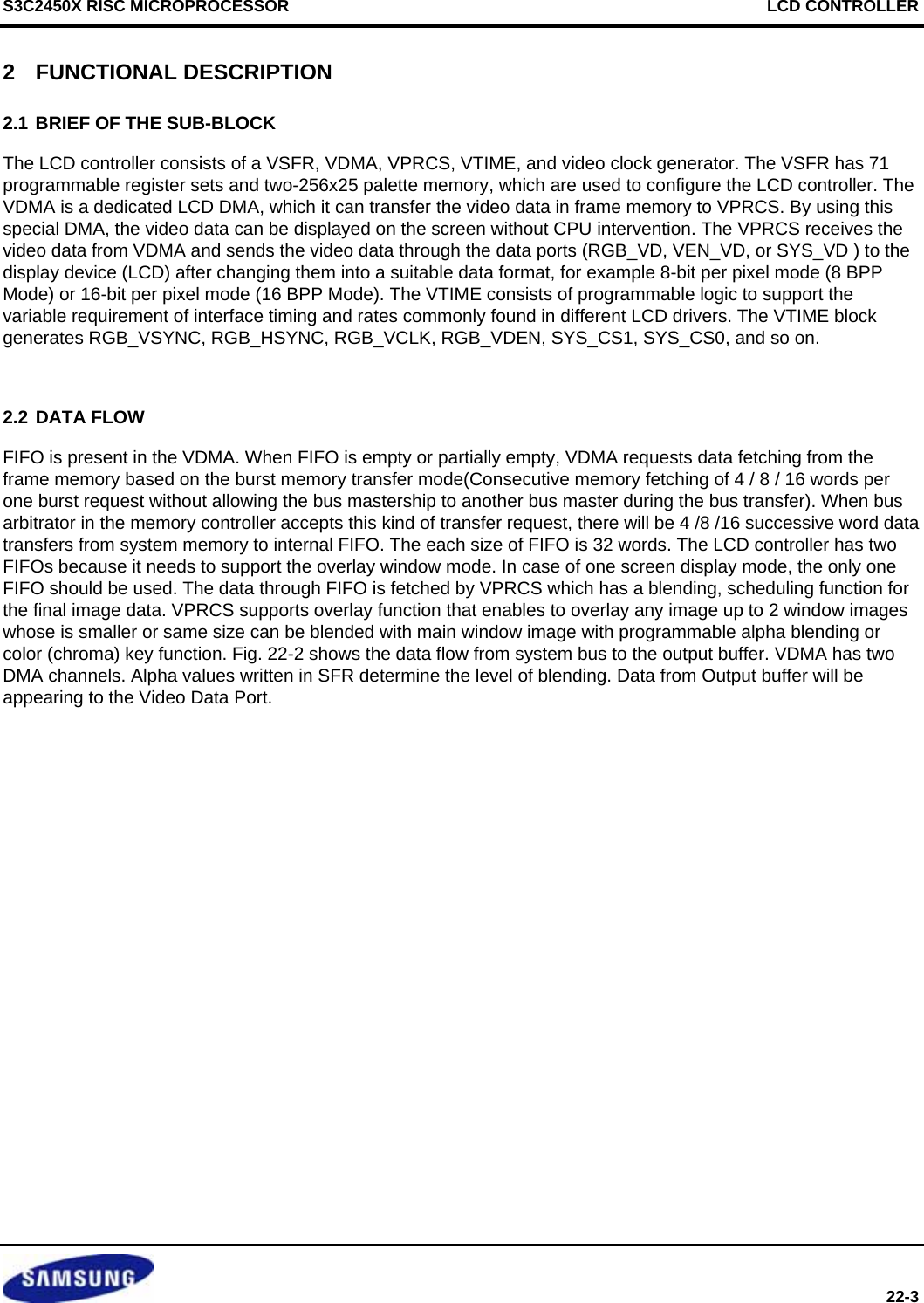
![S3C2450X RISC MICROPROCESSOR LCD CONTROLLER 22-5 2.4 OVERVIEW OF THE COLOR DATA 2.4.1 RGB Data format The LCD controller requests the specified memory format of frame buffer. The next table shows some examples of each display mode. 2.4.2 28BPP display (A4+888) (BSWP = 0, HWSWP = 0, BLD_PIX = 1, ALPHA_SEL = 1) D[31:28] D[27:24] D[23:0] 000H Dummy Bit Alpha value P1 004H Dummy Bit Alpha value P2 008H Dummy Bit Alpha value P3 ... P1 P2 P3 P4 P5 ......LCD Panel NOTE: D[23:16] = Red data, D[15:8] = Green data, D[7:0] = Blue data In case of BLD_PIX and ALPHA_SEL are set, D[27:24] = Alpha value, D[23:16] = Red data, D[15:8] = Green data, D[7:0] = Blue data](https://usermanual.wiki/Diasonic-Technology-Co/RVM-704M.Users-Manual/User-Guide-1826140-Page-577.png)
![LCD CONTROLLER S3C2450X RISC MICROPROCESSOR 22-6 2.4.3 25BPP display (A888) (BSWP = 0, HWSWP = 0) D[31:25] D[24] D[23:0] 000H Dummy Bit AEN P1 004H Dummy Bit AEN P2 008H Dummy Bit AEN P3 ... P1 P2 P3 P4 P5 ......LCD Panel NOTES: 1. AEN : Select Alpha value in Window 1 Alpha Value Register for alpha blending AEN = 0 : ALPHA0_R/G/B values are applied. AEN = 1 : ALPHA1_R/G/B values are applied. Each pixel of LCD panel displays blended color with lower layer window. Refer to the equation of alpha blending on page 22-22. 2. D[23:16] = Red data, D[15:8] = Green data, D[7:0] = Blue data](https://usermanual.wiki/Diasonic-Technology-Co/RVM-704M.Users-Manual/User-Guide-1826140-Page-578.png)
![S3C2450X RISC MICROPROCESSOR LCD CONTROLLER 22-7 2.4.4 24BPP display (A887) (BSWP = 0, HWSWP = 0) D[31:24] D[23] D[22:0] 000H Dummy Bit AEN P1 004H Dummy Bit AEN P2 008H Dummy Bit AEN P3 ... P1 P2 P3 P4 P5 ......LCD Panel NOTES: 1. AEN : Select Alpha value in Window 1 Alpha Value Register for alpha blending AEN = 0 : ALPHA0_R/G/B values are applied. AEN = 1 : ALPHA1_R/G/B values are applied. Each pixel of LCD panel displays blended color with lower layer window. Refer to the equation of alpha blending on page 22-22. 2. D[22:15] = Red data, D[14:7] = Green data, D[6:0] = Blue data](https://usermanual.wiki/Diasonic-Technology-Co/RVM-704M.Users-Manual/User-Guide-1826140-Page-579.png)
![LCD CONTROLLER S3C2450X RISC MICROPROCESSOR 22-8 2.4.5 24BPP display (888) (BSWP = 0, HWSWP = 0) D[31:24] D[23:0] 000H Dummy Bit P1 004H Dummy Bit P2 008H Dummy Bit P3 ... P1 P2 P3 P4 P5 ......LCD Panel NOTE: D[23:16] = Red data, D[15:8] = Green data, D[7:0] = Blue data](https://usermanual.wiki/Diasonic-Technology-Co/RVM-704M.Users-Manual/User-Guide-1826140-Page-580.png)
![S3C2450X RISC MICROPROCESSOR LCD CONTROLLER 22-9 2.4.6 19BPP display (A666) (BSWP = 0, HWSWP = 0) D[31:19] D[18] D[17:0] 000H Dummy Bit AEN P1 004H Dummy Bit AEN P2 008H Dummy Bit AEN P3 ... P1 P2 P3 P4 P5 ......LCD Panel NOTES: 1. AEN : Select Alpha value in Window 1 Alpha Value Register for alpha blending AEN = 0 : ALPHA0_R/G/B values are applied. AEN = 1 : ALPHA1_R/G/B values are applied. Each pixel of LCD panel displays blended color with lower layer window. Refer to the equation of alpha blending on page 22-22. 2. D[17:12] = Red data, D[11:6] = Green data, D[5:0] = Blue data](https://usermanual.wiki/Diasonic-Technology-Co/RVM-704M.Users-Manual/User-Guide-1826140-Page-581.png)
![LCD CONTROLLER S3C2450X RISC MICROPROCESSOR 22-10 2.4.7 18BPP display (666) (BSWP = 0, HWSWP = 0) D[31:18] D[17:0] 000H Dummy Bit P1 004H Dummy Bit P2 008H Dummy Bit P3 ... P1 P2 P3 P4 P5 ......LCD Panel P1 P2 P3 P4 P5 ......LCD Panel NOTE: D[17:12] = Red data, D[11:6] = Green data, D[5:0] = Blue data](https://usermanual.wiki/Diasonic-Technology-Co/RVM-704M.Users-Manual/User-Guide-1826140-Page-582.png)
![S3C2450X RISC MICROPROCESSOR LCD CONTROLLER 22-11 2.4.8 16BPP display (A555) (BSWP = 0, HWSWP = 0) D[31] D[30:16] D[15] D[14:0] 000H AEN1 P1 AEN2 P2 004H AEN3 P3 AEN4 P4 008H AEN5 P5 AEN6 P6 ... (BSWP = 0, HWSWP = 1) [31] D[30:16] D[15] D[14:0] 000H AEN2 P2 AEN1 P1 004H AEN4 P4 AEN3 P3 008H AEN6 P6 AEN5 P5 ... P1 P2 P3 P4 P5 ......LCD Panel NOTES: 1. AEN : Select Alpha value in Window 1 Alpha Value Register for alpha blending AEN = 0 : ALPHA0_R/G/B values are applied. AEN = 1 : ALPHA1_R/G/B values are applied. Each pixel of LCD panel displays blended color with lower layer window. Refer to the equation of alpha blending on page 22-22. 2. D[14:10] = Red data, D[9:5] = Green data, D[4:0] = Blue data](https://usermanual.wiki/Diasonic-Technology-Co/RVM-704M.Users-Manual/User-Guide-1826140-Page-583.png)
![LCD CONTROLLER S3C2450X RISC MICROPROCESSOR 22-12 2.4.9 16BPP display (1+555) (BSWP = 0, HWSWP = 0) D[31:16] D[15:0] 000H P1 P2 004H P3 P4 008H P5 P6 ... (BSWP = 0, HWSWP = 1) D[31:16] D[15:0] 000H P2 P1 004H P4 P3 008H P6 P5 ... NOTE: {D[14:10], D[15] } = Red data, {D[9:5], D[15] } = Green data, {D[4:0], D[15]}= Blue data Figure 22-3. 16BPP(1+5:5:5, BSWP/HWSWP=0) Display Types](https://usermanual.wiki/Diasonic-Technology-Co/RVM-704M.Users-Manual/User-Guide-1826140-Page-584.png)
![S3C2450X RISC MICROPROCESSOR LCD CONTROLLER 22-13 2.4.10 16BPP display (565) (BSWP = 0, HWSWP = 0) D[31:16] D[15:0] 000H P1 P2 004H P3 P4 008H P5 P6 ... (BSWP = 0, HWSWP = 1) D[31:16] D[15:0] 000H P2 P1 004H P4 P3 008H P6 P5 ... NOTE: D[15:11] = Red data, D[10:5] = Green data, D[4:0] = Blue data Figure 22-4. 16BPP(5:6:5, BSWP/HWSWP=0) Display Types](https://usermanual.wiki/Diasonic-Technology-Co/RVM-704M.Users-Manual/User-Guide-1826140-Page-585.png)
![LCD CONTROLLER S3C2450X RISC MICROPROCESSOR 22-14 2.4.11 8BPP display (A232) (BSWP = 0, HWSWP = 0) D[31] D[30:24] D[23] D[22:16] D[15] D[14:8] D[7] D[6:0] 000H AEN1 P1 AEN2 P2 AEN3 P3 AEN4 P4 004H AEN5 P5 AEN6 P6 AEN7 P7 AEN8 P8 008H AEN9 P9 AEN10 P10 AEN11 P11 AEN12 P12 ... (BSWP = 1, HWSWP = 0) D[31] D[30:24] D[23] D[22:16] D[15] D[14:8] D[7] D[6:0] 000H AEN4 P4 AEN3 P3 AEN2 P2 AEN1 P1 004H AEN8 P8 AEN7 P7 AEN6 P6 AEN5 P5 008H AEN12 P12 AEN11 P11 AEN10 P10 AEN9 P9 ... P1 P2 P3 P4 P5 ......LCD PanelP6 P7 P8 P10 P11 P12P9 NOTES: 1. AEN : Select Alpha value in Window 1 Alpha Value Register for alpha blending AEN = 0 : ALPHA0_R/G/B values are applied. AEN = 1 : ALPHA1_R/G/B values are applied. Each pixel of LCD panel displays blended color with lower layer window. Refer to the equation of alpha blending on page 22-22. 2. D[6:5] = Red data, D[4:2] = Green data, D[1:0] = Blue data](https://usermanual.wiki/Diasonic-Technology-Co/RVM-704M.Users-Manual/User-Guide-1826140-Page-586.png)
![S3C2450X RISC MICROPROCESSOR LCD CONTROLLER 22-15 2.4.12 8BPP display (Palette) (BSWP = 0, HWSWP = 0) D[31:24] D[23:16] D[15:8] D[7:0] 000H P1 P2 P3 P4 004H P5 P6 P7 P8 008H P9 P10 P11 P12 ... (BSWP = 1, HWSWP = 0) D[31:24] D[23:16] D[15:8] D[7:0] 000H P4 P3 P2 P1 004H P8 P7 P6 P5 008H P12 P11 P10 P9 ... P1 P2 P3 P4 P5 ......LCD PanelP6 P7 P8 P10 P11 P12P9 NOTE: The values of frame buffer are index of palette memory. The MSB value of Palette memory is AEN bit. AEN : Select Alpha value in Window 1 Alpha Value Register for alpha blending AEN = 0 : ALPHA0_R/G/B values are applied. AEN = 1 : ALPHA1_R/G/B values are applied. Each pixel of LCD panel displays blended color with lower layer window. Refer to the equation of alpha blending on page 22-22.](https://usermanual.wiki/Diasonic-Technology-Co/RVM-704M.Users-Manual/User-Guide-1826140-Page-587.png)
![LCD CONTROLLER S3C2450X RISC MICROPROCESSOR 22-16 2.4.13 4BPP display (Palette) (BSWP = 0, HWSWP = 0) D[31:28] D[27:24] D[23:20] D[19:16] D[15:12] D[11:8] D[7:4] D[3:0] 000H P1 P2 P3 P4 P5 P6 P7 P8 004H P9 P10 P11 P12 P13 P14 P15 P16 008H P17 P18 P19 P20 P21 P22 P23 P24 ... (BSWP = 1, HWSWP = 0) D[31:28] D[27:24] D[23:20] D[19:16] D[15:12] D[11:8] D[7:4] D[3:0] 000H P7 P8 P5 P6 P3 P4 P1 P2 004H P15 P16 P13 P14 P11 P12 P9 P10 008H P23 P24 P21 P22 P19 P20 P17 P18 ... NOTE: The values of frame buffer are index of palette memory. The MSB value of Palette memory is AEN bit. AEN : Select Alpha value in Window 1 Alpha Value Register for alpha blending AEN = 0 : ALPHA0_R/G/B values are applied. AEN = 1 : ALPHA1_R/G/B values are applied. Each pixel of LCD panel displays blended color with lower layer window. Refer to the equation of alpha blending on page 22-22.](https://usermanual.wiki/Diasonic-Technology-Co/RVM-704M.Users-Manual/User-Guide-1826140-Page-588.png)
![S3C2450X RISC MICROPROCESSOR LCD CONTROLLER 22-17 2.4.14 2BPP display (Palette) (BSWP = 0, HWSWP = 0) [31:30] [29:28] [27:26] [25:24] [23:22] [21:20] [19:18] [17:16] 002H P1 P2 P3 P4 P5 P6 P7 P8 006H P17 P18 P19 P20 P21 P22 P23 P24 00AH P33 P34 P35 P36 P37 P38 P39 P40 … [15:14] [13:12] [11:10] [9:8] [7:6] [5:4] [3:2] [1:0] 000H P9 P10 P11 P12 P13 P14 P15 P16 004H P25 P26 P27 P28 P29 P30 P31 P32 008H P41 P42 P43 P44 P45 P46 P47 P48 ... 2.4.15 1BPP display (Palette) (BSWP = 0, HWSWP = 0) [31] [30] [29] [28] [27] [26] [25] [24] [23] [22] [21] [20] [19] [18] [17] [16]002H P1 P2 P3 P4 P5 P6 P7 P8 P9 P10 P11 P12 P13 P14 P15 P16006H P33 P34 P35 P36 P37 P38 P39 P40 P41 P42 P43 P44 P45 P46 P47 P48… [15] [14] [13] [12] [11] [10] [9] [8] [7] [6] [5] [4] [3] [2] [1] [0]000H P17 P18 P19 P20 P21 P22 P23 P24 P25 P26 P27 P28 P29 P30 P31 P32004H P49 P50 P51 P52 P53 P54 P55 P56 P57 P58 P59 P60 P61 P62 P63 P64… NOTE: The values of frame buffer are index of palette memory. The MSB value of Palette memory is AEN bit. AEN : Select Alpha value in Window 1 Alpha Value Register for alpha blending AEN = 0 : ALPHA0_R/G/B values are applied. AEN = 1 : ALPHA1_R/G/B values are applied. Each pixel of LCD panel displays blended color with lower layer window. Refer to the equation of alpha blending on page 22-22.](https://usermanual.wiki/Diasonic-Technology-Co/RVM-704M.Users-Manual/User-Guide-1826140-Page-589.png)
![LCD CONTROLLER S3C2450X RISC MICROPROCESSOR 22-18 2.5 VD SIGNAL CONNECTION 2.5.1 VD Pin Descriptions at 24BPP RGB parallel VD 23 22 21 20 19 18 17 16 15 14 13 12 11 10 9876 5 4 3 2 1 0RED 7 6 5 4 3 2 1 0 GREEN 76543210 BLUE 76 5 4 3 210 2.5.2 VD Pin Descriptions at 18BPP RGB parallel VD 23 22 21 20 19 18 17 16 15 14 13 12 11 10 9876 5 4 3 2 1 0RED 5 4 3 2 1 0 GREEN 543210 BLUE NC NC 5 4 3 2 1 0NC 2.5.3 VD Pin Descriptions at 16BPP RGB parallel (5:6:5) VD 23 22 21 20 19 18 17 16 15 14 13 12 11 10 9876 5 4 3 2 1 0RED 4 3 2 1 0 GREEN 543210 BLUE NC NC 4 3 2 1 0 NC 2.5.4 VD Pin Descriptions at 24BPP RGB Serial (8+8+8) VD 23 22 21 20 19 18 17 16 [15:0] 1st time 7 6 5 4 3 2 1 0 2nd time 7 6 5 4 3 2 1 0 3rd time 7 6 5 4 3 2 1 0 NC 2.5.5 VD Pin Descriptions at 18BPP RGB Serial (6+6+6) VD 23 22 21 20 19 18 [17:0] 1st time 5 4 3 2 1 0 2nd time 5 4 3 2 1 0 3rd time 5 4 3 2 1 0 NC](https://usermanual.wiki/Diasonic-Technology-Co/RVM-704M.Users-Manual/User-Guide-1826140-Page-590.png)
![LCD CONTROLLER S3C2450X RISC MICROPROCESSOR 22-20 2.6 PALETTE USAGE 2.6.1 Palette Configuration and Format Control The LCD controller can support the 256 colors palette for various selection of color mapping. The user can select 256 colors from the 24-bit colors through these four formats. 256 colors palette consist of the 256(depth) × 25-bit DPSRAM. Palette supports 8:8:8, 6:6:6, 5:6:5(R:G:B), and etc format. For example of A:5:5:5 format, write palette like Table 22-3 and then connect VD pin to LCD panel( R(5)=VD[23:19], G(5)=VD[15:11], and B(5)=VD[7:3] ). Select Alpha value in Window 1 Alpha Value Register. At the last, Set Window Palette Control(W0PAL, case window0) register to 0’b101. Table 22-1. 25BPP(A:8:8:8) Palette Data Format INDEX\Bit Pos. 24 23 22 21 20 19 18 17 16 15 14 13 12 11 10 9 8 7 6 5 4 3 2 1 0 00H AEN R7 R6 R5 R4 R3 R2 R1 R0 G7 G6 G5 G4 G3 G2 G1 G0 B7 B6 B5 B4 B3 B2 B1 B001H AEN R7 R6 R5 R4 R3 R2 R1 R0 G7 G6 G5 G4 G3 G2 G1 G0 B7 B6 B5 B4 B3 B2 B1 B0....... … … … … … … … … … ………………………… … … … ………FFH AEN R7 R6 R5 R4 R3 R2 R1 R0 G7 G6 G5 G4 G3 G2 G1 G0 B7 B6 B5 B4 B3 B2 B1 B0Number of VD - 23 22 21 20 19 18 17 16 15 14 13 12 11 10 9 8 7 6 5 4 3 2 1 0](https://usermanual.wiki/Diasonic-Technology-Co/RVM-704M.Users-Manual/User-Guide-1826140-Page-592.png)
![LCD CONTROLLER S3C2450X RISC MICROPROCESSOR 22-22 3 WINDOW BLENDING 3.1 OVERVIEW The main function of the VPRCS module is window blending. LCD controller has 2-window layers and the detail is described below. As an example of application, System can use win0 as an OS window, full TV screen window or etc. This feature enhances the system performance by reducing the data rate of total system. 3.1.1 Total 2 windows Window 0 (base) : RGB with palette Window 1 (overlay) : RGB with palette 3.1.2 Overlay Priority Win 1 > Win 0 3.1.3 Blending equation WinOut(R) = Win0(R) x (1-AR) + Win1(R) x AR WinOut(G) = Win0(G) x (1-AG) + Win1(G) x AG WinOut(B) = Win0(B) x (1-AB) + Win1(B) x AB Where, AR = Win1’s Red blending factor(ALPHA0_R/16 or ALPHA1_R/16 or DATA[27:24]/16, AR range is 0~1) AG = Win1’s Green blending factor(ALPHA0_G/16 or ALPHA1_G/16 or DATA[27:24]/16, AG range is 0~1) AB = Win1’s Blue blending factor(ALPHA0_B/16 or ALPHA1_B/16 or DATA[27:24]/16, AB range is 0~1) Figure 22-5. Blending Operations](https://usermanual.wiki/Diasonic-Technology-Co/RVM-704M.Users-Manual/User-Guide-1826140-Page-594.png)
![S3C2450X RISC MICROPROCESSOR LCD CONTROLLER 22-23 3.2 BLENDING DIAGRAM/DETAILS LCD controller could blend 2-Layer for the only one pixel at the same time. The Blending factor, alpha value is controlled by ALPHA0_R/G/B and ALPHA1_R/G/B fields in Window 1 Alpha Value register or DATA[27:24] in frame buffer, which are implemented for each window layer and color(R,G,B). As a special feature, between two windows have two kinds of alpha blending value. One is ALPHA0_R/G/B(AEN=0) and the other is ALPHA1_R/G/B(AEN=1). Table 22-4. Alpha Value Selection Table for Blending ALPHA_SEL = 0 @WINCON1[1] ALPHA0_R/G/B BLD_PIX = 0 (WINCON1[6]) ALPHA_SEL = 1 @WINCON1[1] ALPHA1_R/G/B AEN = 0 ALPHA0_R/G/B KEYBLEND = 0 @W1KEYCON0[26] AEN = 1 ALPHA1_R/G/B Non-Key area ALPHA0_R/G/B ALPHA_SEL = 0 @WINCON1[1] KEYBLEND = 1 @W1KEYCON0[26] Key area ALPHA1_R/G/B BLD_PIX = 1 @WINCON1[6] ALPHA_SEL = 1 @WINCON1[1] DATA[27:24] in frame buffer for 28bpp mode 3.2.1 COLOR-KEY FUNCTION The LCD controller can support color-key function for the various effect of image mapping. Color image of OSD layer, which is specified by COLOR-KEY register, will be substituted by background image for special functionality, as cursor image or pre-view image of the camera. The register value to ColorKey reg must be set in 24bit RGB format. DIRCON (in Win1 Color Key 0 register) bit selects the window to be compared with COLVAL (in Win1 Color Key 1 Register). If this bit is set to ‘0’, the comparison window is window1 (foreground window). COMPKEY (in Win1 Color Key 0 register) value decides whether to compare COLVAL and selected window color. In other words, the comparator only compares COLVAL and selected window color bits where the corresponding bit in COMPKEY is ‘0’.](https://usermanual.wiki/Diasonic-Technology-Co/RVM-704M.Users-Manual/User-Guide-1826140-Page-595.png)
![LCD CONTROLLER S3C2450X RISC MICROPROCESSOR 22-26 4 VTIME CONTROLLER OPERATION 4.1 RGB INTERFACE The VTIME generates the control signals such as, RGB_VSYNC, RGB_HSYNC, RGB_VDEN and RGB_VCLK signal for RGB interface. These control signals are highly related with the configuration on the VIDTCON0/1/2 registers in the VSFR register. Base on these programmable configurations of the display control registers in VSFR, the VTIME module can generate the programmable control signals suitable for the support of many different types of display device. The RGB_VSYNC signal is asserted to cause the LCD's line pointer to start over at the top of the display. The RGB_VSYNC and RGB_HSYNC pulse generation is controlled by the configuration of both the HOZVAL field and the LINEVAL registers. The HOZVAL and LINEVAL can be determined by the size of the LCD panel according to the following equations: HOZVAL = (Horizontal display size) -1 LINEVAL = (Vertical display size) –1 The rate of RGB_VCLK signal can be controlled by the CLKVAL field in the VIDCON0 register. The table below defines the relationship of RGB_VCLK and CLKVAL. The minimum value of CLKVAL is 1. RGB_VCLK (Hz) =HCLK/ [CLKVAL+1] Table 22-5. Relation between VCLK and CLKVAL (Freq. of Video Clock Source=60MHz) CLKVAL 60MHz/X VCLK 1 60 MHz/2 30.0 MHz 2 60 MHz/3 15.0 MHz : : : 63 60 MHz/64 938 kHz The RGB_HSYNC and RGB_VSYNC signal is configured by RGB_VSYNC, VBPD, VFPD, HSYNC, HBPD, HFPD, HOZVAL and LINEVAL. Refer the Figure 22-10. The frame rate is RGB_VSYNC signal frequency. The frame rate is related with the field of RGB_VSYNC, VBPD, VFPD, LINEVAL, HSYNC, HBPD, HFPD, HOZVAL, CLKVAL registers. Most LCD drivers need their own adequate frame rate. The frame rate is calculated as follows; Frame Rate = 1/ [ { (VSPW+1) + (VBPD+1) + (LIINEVAL + 1) + (VFPD+1) } x {(HSPW+1) + (HBPD +1) + (HFPD+1) + (HOZVAL + 1) } x { (CLKVAL+1 ) / ( Frequency of Clock source ) } ] 4.2 i80-SYSTEM INTERFACE The VTIME generates the control signals such as, SYS_CS0, SYS_CS1, SYS_RS and SYS_WE signal for i80-System Interface. The LCDIFMODE, LCD_CS_SETUP, LCD_WAIT_WR and LCD_HOLD_WR registers control these signals. Refer to figure 22-11.](https://usermanual.wiki/Diasonic-Technology-Co/RVM-704M.Users-Manual/User-Guide-1826140-Page-598.png)
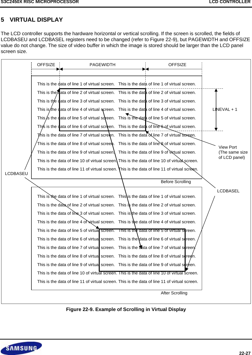
![LCD CONTROLLER S3C2450X RISC MICROPROCESSOR 22-28 6 RGB INTERFACE I/O 6.1.1 Signals Name Type Description RGB_HSYNC Output Horizontal Sync. Signal RGB_VSYNC Output Vertical Sync. Signal RGB_VCLK Output LCD Video Clock RGB_VDEN Output Data Enable RGB_VD[23:0] Output RGB data output 6.1.2 RGB I/F Timing VSPW+1 VBPD+1 LINEVAL+1 VFPD+11 FRAMEINT_FrSyn(internal)RGB_VSYNCRGB_HSYNCRGB_VDEN~~~~~~~~~~~~1 LINE~~~~HSPW+1 HBPD+1 HOZVAL+1 HFPD+1RGB_HSYNCRGB_VCLKRGB_VDRGB_VDENVSPW=0, VBPD=0, VFPD=0, HSPW=1, HBPD=1, HFPD=1 Figure 22-10. LCD RGB Interface Timing](https://usermanual.wiki/Diasonic-Technology-Co/RVM-704M.Users-Manual/User-Guide-1826140-Page-600.png)
![S3C2450X RISC MICROPROCESSOR LCD CONTROLLER 22-29 7 LCD CPU INTERFACE I/O (i80-SYSTEM I/F) 7.1.1 Signals Name Type Description SYS_VD[17:0] InOut Video Data SYS_CS0 Output Chip select for Main LCD SYS_CS1 Output Chip select for Sub LCD SYS_WR Output Write enable SYS_OE Output Output enable SYS_RS Output Register/State select 7.1.2 CPU (i80-System) I/F Timing Figure 22-11. Write Cycle Timing](https://usermanual.wiki/Diasonic-Technology-Co/RVM-704M.Users-Manual/User-Guide-1826140-Page-601.png)
![LCD CONTROLLER S3C2450X RISC MICROPROCESSOR 22-30 7.1.3 LCD signal Muxing Table 22-6. LCD Signal Muxing Table (RGB and i-80 I/F) PAD VIDOUT Signals 10/11 SYS_WR 01 Reserved RGB_VCLK/SYS_WR 00 RGB_VCLK 10/11 SYS_CS0 01 Reserved RGB_HSYNC/SYS_CS0 00 RGB_HSYNC 10/11 SYS_CS1 01 Reserved RGB_VSYNC/SYS_CS1 00 RGB_VSYNC 10/11 SYS_RS 01 Reserved RGB_VDEN/SYS_RS 00 RGB_VDEN 10/11 SYS_OE 01 Reserved RGB_LEND/SYS_OE 00 RGB_LEND 10/11 SYS_VD 01 Reserved RGB_VD/SYS_VD 00 RGB_VD • VIDOUT values are defined in VIDCON0[23:22]](https://usermanual.wiki/Diasonic-Technology-Co/RVM-704M.Users-Manual/User-Guide-1826140-Page-602.png)
![S3C2450X RISC MICROPROCESSOR LCD CONTROLLER 22-33 8.1.2 Video Main Control 0 Register Register Address R/W Description Reset ValueVIDCON0 0x4C800000 R/W Video control 1 register 0x0000_0000 VIDCON0 Bit Description Initial StateReserved [31:24] Reserved 0x00 VIDOUT [23:22] It determines the output format of LCD Controller 00 = RGB I/F 01 = Reserved 10 = i80-System I/F for Main LDI 11 = i80-System I/F for Sub LDI 0 L1_DATA16 [21:19] Select the mode of output data format of i80-System I/F (Sub LDI.) (Only when, VIDOUT == 2’b11) 000 = 16-bit mode (16 bpp) 001 = 16 + 2 bit mode (18 bpp) 010 = 9 + 9 bit mode (18 bpp) 011 = 16 + 8 bit mode (24 bpp) 100 = 18-bit mode (18bpp) 000 L0_DATA16 [18:16] Select the mode of output data format of i80-System I/F (Main LDI.) (Only when, VIDOUT == 2’b10) 000 = 16 bit mode (16 bpp) 001 = 16 + 2 bit mode (18 bpp) 010 = 9 + 9 bit mode (18 bpp) 011 = 16 + 8 bit mode (24 bpp) 100 = 18 bit mode (18bpp) 000 Reserved [15] Reserved 0 PNRMODE [14:13] Select the display mode. (Where, VIDOUT == 2’b00) 00 = RGB Parallel format (RGB) 01 = RGB Parallel format (BGR) 10 = Serial Format (R->G->B) 11 = Serial Format (B->G->R) Select the display mode. (Where, VIDOUT == 2’b1x) 00 = RGB Parallel format (RGB) 00](https://usermanual.wiki/Diasonic-Technology-Co/RVM-704M.Users-Manual/User-Guide-1826140-Page-605.png)
![LCD CONTROLLER S3C2450X RISC MICROPROCESSOR 22-34 8.1.3 Video Main Control 0 Register (Continued) VIDCON0 Bit Description Initial StateCLKVALUP [12] Select CLKVAL_F Update timing control 0 = Always 1 = Start of a frame (Only once per frame) 0 CLKVAL_F [11:6] Determine the rates of VCLK. VCLK = (HCLK or LCD video Clock) / [CLKVAL+1] ( CLKVAL ≥ 1 ) 0 VCLKEN [5] VCLK Enable Control 0 = Disable 1 = Enable 0 CLKDIR [4] Select the clock source as direct or divide using CLKVAL_F register. 0 = Direct clock (frequency of VCLK = frequency of Clock source) 1 = Divided using CLKVAL_F 0 CLKSEL_F [3:2] Select the Video Clock source 00 = HCLK 01 = LCD video Clock (from SYSCON EPLL) 10 = Reserved 11 = Reserved 0 ENVID [1:0] Video output and the LCD logics enable/disable control. 00 = Disable video signals and logics immediately. 01 = Reserved. 10 = Disable video signals and logics at the end of current frame. 11 = Enable video output and logics. Note : If set to ‘10b’ in the middle of displaying current frame, the value of ENVID is still ‘11b’. However, the LCD functions are disabled at the end of current frame and the value is changed to ‘10b’. 0](https://usermanual.wiki/Diasonic-Technology-Co/RVM-704M.Users-Manual/User-Guide-1826140-Page-606.png)
![S3C2450X RISC MICROPROCESSOR LCD CONTROLLER 22-35 8.1.4 Video Main Control 1 Register Register Address R/W Description Reset ValueVIDCON1 0x4C800004 R/W Video control 2 register 0x0000_0000 VIDCON1 Bit Description Initial state LINECNT (read only) [26:16] Provide the status of the line counter (read only) Up count from 0 to LINEVAL 0 Reserved [15] Reserved 0 VSTATUS [14:13] Vertical Status (read only). 00 = VSYNC 01 = BACK Porch 10 = ACTIVE 11 = FRONT Porch 0 HSTATUS [12:11] Horizontal Status (read only). 00 = HSYNC 01 = BACK Porch 10 = ACTIVE 11 = FRONT Porch 0 Reserved [10:8] Reserved IVCLK [7] This bit controls the polarity of the VCLK active edge. 0 = The video data is fetched at VCLK falling edge 1 = The video data is fetched at VCLK rising edge 0 IHSYNC [6] This bit indicates the HSYNC pulse polarity. 0 = normal(active high) 1 = inverted(active low) 0 IVSYNC [5] This bit indicates the VSYNC pulse polarity. 0 = normal(active high) 1 = inverted(active low) 0 IVDEN [4] This bit indicates the VDEN signal polarity. 0 = normal(active high) 1 = inverted(active low) 0 Reserved [3:0] Reserved 0x0 8.1.5 VIDEO Time Control 0 Register Register Address R/W Description Reset ValueVIDTCON0 0x4C800008 R/W Video time control 1 register 0x0000_0000 VIDTCON0 Bit Description Initial StateVBPD [23:16] Vertical back porch is the number of inactive lines at the start of a frame, after vertical synchronization period. (Period : VBPD +1) 0x00 VFPD [15:8] Vertical front porch is the number of inactive lines at the end of a frame, before vertical synchronization period. (Period : VFPD +1) 0x00 VSPW [7:0] Vertical sync pulse width determines the VSYNC pulse's level width by counting the number of inactive lines. (Period : VSPW +1) 0x00](https://usermanual.wiki/Diasonic-Technology-Co/RVM-704M.Users-Manual/User-Guide-1826140-Page-607.png)
![LCD CONTROLLER S3C2450X RISC MICROPROCESSOR 22-36 8.1.6 Video Time Control 1 Register Register Address R/W Description Reset ValueVIDTCON1 0x4C80000C R/W Video time control 2 register 0x0000_0000 VIDTCON1 Bit Description Initial state HBPD [23:16] Horizontal back porch is the number of VCLK periods between the edge of HSYNC and the start of active data. (Period : HBPD +1) Note: Set 0x10 for i80-System Interface When the PNRMODE (VIDCON0 [14:13]) is set to serial format the period becomes 3 times of HBPD value. (If HBPD is set to ‘0’ in serial mode, the period becomes 3-VLCK) 0000000 HFPD [15:8] Horizontal front porch is the number of VCLK periods between the end of active data and the edge of next HSYNC. (Period : HFPD +1) Note: When the PNRMODE(VIDCON0[14:13]) is set to serial format the period of HFPD becomes 3 times of VCLK (If HFPD is set to ‘0’ in serial mode, the period becomes 3-VLCK) 0x00 HSPW [7:0] Horizontal sync pulse width determines the HSYNC pulse's level width by counting the number of the VCLK. (Period : HSPW +1) Note: When the PNRMODE(VIDCON0[14:13]) is set to serial format the period of HSPW becomes 3 times of VCLK (If HSPW is set to ‘0’ in serial mode, the period becomes 3-VLCK) 0x00 8.1.7 VIDEO Time Control 2 Register Register Address R/W Description Reset ValueVIDTCON2 0x4C800010 R/W Video time control 3 register 0x0000_0000 VIDTCON2 Bit Description Initial state LINEVAL [21:11] These bits determine the vertical size of display 0 HOZVAL [10:0] These bits determine the horizontal size of display 0](https://usermanual.wiki/Diasonic-Technology-Co/RVM-704M.Users-Manual/User-Guide-1826140-Page-608.png)
![S3C2450X RISC MICROPROCESSOR LCD CONTROLLER 22-37 8.1.8 Window 0 Control Register Register Address R/W Description Reset ValueWINCON0 0x4C800014 R/W Window 0 control register 0x0000_0000 WINCON0 Bit Description Initial State BUFSTATUS [24] Status of Current display Buffer (Read only) 0 = buffer0 display 1 = buffer1 display Note: RGB I/F does not support auto-change mode. Only i80-Sytem I/F supports auto-change mode. 0 BUFSEL [23] Select Buffer selection control 0 = buffer0 select 1 = buffer1 select 0 BUFAUTOEN [22] Double Buffer Auto-change control bit 0 = Fixed by BUFSEL 1 = Auto changed by SWTRIG (in CPUTRIGCON2 register) Note: RGB I/F does not support auto-change mode. Only i80-Sytem I/F supports auto-change mode. 0 BITSWP [18] Bit swap control bit. 0 = Swap Disable 1 = Swap Enable 0 BYTSWP [17] Byte swaps control bit. 0 = Swap Disable 1 = Swap Enable 0 HAWSWP [16] Half-Word swap control bit. 0 = Swap Disable 1 = Swap Enable 0 Reserved [15:11] Reserved 0 BURSTLEN [10:9] DMA’s Burst Length selection: 00 = 16 word– burst 01 = 8 word– burst 10 = 4 word– burst 11 = Reserved 0 Reserved [8:6] Reserved 0 BPPMODE_F [5:2] Select the BPP (Bits Per Pixel) mode Window image. 0000 = 1bpp ( palletized ) 0001 = 2bpp ( palletized ) 0010 = 4bpp ( palletized ) 0011 = 8bpp ( palletized ) 0100 = Reserved 0101 = 16bpp (non-palletized, R: 5-G:6-B:5 ) 0110 = Reserved 0111 = 16 bpp (non-palletized, I :1-R:5-G:5-B:5 ) 1000 = Unpacked 18bpp (non-palletized, R:6-G:6-B:6 ) 1001 = Reserved 1010 = Reserved 1011 = Unpacked 24bpp ( non-palletized R:8-G:8-B:8 ) 11xx = Reserved 0 Reserved [1] Reserved 0 ENWIN_F [0] Window0 on/ off control 0 = Off window0. 1 = On window0. 0](https://usermanual.wiki/Diasonic-Technology-Co/RVM-704M.Users-Manual/User-Guide-1826140-Page-609.png)
![LCD CONTROLLER S3C2450X RISC MICROPROCESSOR 22-38 8.1.9 Window 1 Control Register Register Address R/W Description Reset ValueWINCON1 0x4C800018 R/W Window control 1 register 0x0000_0000 WINCON1 Bit Description Initial StateBITSWP [18] Bit swap control 0 = Swap Disable 1 = Swap Enable 0 BYTSWP [17] Byte swaps control 0 = Swap Disable 1 = Swap Enable 0 HAWSWP [16] Half-Word swap control 0 = Swap Disable 1 = Swap Enable 0 − [15:11] Reserved 0 BURSTLEN [10:9] DMA’s Burst Length selection : 00 = 16 word– burst 01 = 8 word– burst 10 = 4 word– burst 11 = Reserved 0 Reserved [8:7] Reserved 0 BLD_PIX [6] Select blending category 0 = Per plane blending 1 = Per pixel blending 0 BPPMODE_F [5:2] Select the BPP (Bits Per Pixel) mode Window image. 0000 = 1bpp ( palletized ) 0001 = 2bpp ( palletized ) 0010 = 4bpp ( palletized ) 0011 = 8bpp ( palletized ) 0100 = 8bpp ( non-palletized, A: 1-R:2-G:3-B:2 ) 0101 = 16bpp ( non-palletized, R:5-G:6-B:5 ) 0110 = 16bpp ( non-palletized, A:1-R:5-G:5-B:5 ) 0111 = 16bpp ( non-palletized, I :1-R:5-G:5-B:5 ) 1000 = Unpacked 18bpp ( non-palletized, R:6-G:6-B:6 ) 1001 = Unpacked 18bpp ( non-palletized, A:1-R:6-G:6-B:5 ) 1010 = Unpacked 19bpp ( non-palletized, A:1-R:6-G:6-B:6 ) 1011 = Unpacked 24bpp ( non-palletized, R:8-G:8-B:8 ) 1100 = Unpacked 24bpp ( non-palletized, A:1-R:8-G:8-B:7 ) 1101 = Unpacked 25bpp ( non-palletized, A:1-R:8-G:8-B:8 ) or Unpacked 28bpp ( non-palletized, A:4-R:8-G:8-B:8 ) 111x = Reserved Note: 1101 = support 28bpp (non-palletized A:4-R:8-G:8-B:8 ) for per pixel blending. 0 ALPHA_SEL [1] Alpha value selection Per plane blending case( BLD_PIX ==0) 0 = using ALPHA0_R/G/B values 1 = using ALPHA1_R/G/B values 0](https://usermanual.wiki/Diasonic-Technology-Co/RVM-704M.Users-Manual/User-Guide-1826140-Page-610.png)
![S3C2450X RISC MICROPROCESSOR LCD CONTROLLER 22-39 WINCON1 Bit Description Initial StatePer pixel blending case( BLD_PIX ==1) 0 = selected by AEN bit in frame buffer for each pixel or Key area AEN = 0 ALPHA0_R/G/B 0 AEN = 1 ALPHA1_R/G/B Non-Key area ALPHA0_R/G/B KEYBLEND (W1KEYCON0[26]) 1 Key area ALPHA1_R/G/B 1 = using DATA[27:24] in frame buffer, only for 28bpp mode ENWIN_F [0] Window1 on/ off control 0 = Off window1 1 = On window1 0 8.1.10 Window 0 Position Control A Register Register Address R/W Description Reset ValueVIDOSD0A 0x4C800028 R/W Video Window 0’s position control register 0x0000_0000 VIDOSD0A Bit Description Initial State OSD_LeftTopX_F [21:11] Horizontal screen coordinate for left top pixel of OSD image 0 OSD_LeftTopY_F [10:0] Vertical screen coordinate for left top pixel of OSD image 0 8.1.11 Window 0 Position Control B Register Register Address R/W Description Reset ValueVIDOSD0B 0x4C80002C R/W Video Window 0’s position control register 0x0000_0000 VIDOSD0B Bit Description Initial State OSD_RightBotX_F [21:11] Horizontal screen coordinate for right bottom pixel of OSD image 0 OSD_RightBotY_F [10:0] Vertical screen coordinate for right bottom pixel of OSD image 0 NOTE: Registers must have word boundary X position. So, 24bpp mode should have X position by 1 pixel. ( ex, X = 0,1,2,3….) 16bpp mode should have X position by 2 pixel. ( ex, X = 0,2,4,6….) 8bpp mode should have X position by 4 pixel. ( ex, X = 0,4,8,12….)](https://usermanual.wiki/Diasonic-Technology-Co/RVM-704M.Users-Manual/User-Guide-1826140-Page-611.png)
![LCD CONTROLLER S3C2450X RISC MICROPROCESSOR 22-40 8.1.12 Window 1 Position Control A Register Register Address R/W Description Reset ValueVIDOSD1A 0x4C800034 R/W Video Window 1’s position control 2 register 0x0000_0000 VIDOSD1A Bit Description initial state OSD_LeftTopX_F [21:11] Horizontal screen coordinate for left top pixel of OSD image 0 OSD_LeftTopY_F [10:0] Vertical screen coordinate for left top pixel of OSD image 0 8.1.13 Window 1 Position Control B Register Register Address R/W Description Reset ValueVIDOSD1B 0x4C800038 R/W Video Window 1’s position control register 0x0000_0000 VIDOSD1B Bit Description Initial state OSD_RightBotX_F [21:11] Horizontal screen coordinate for right bottom pixel of OSD image 0 OSD_RightBotY_F [10:0] Vertical screen coordinate for right bottom pixel of OSD image 0 NOTE: Registers must have word boundary X position. So, 24bpp mode should have X position by 1 pixel. ( ex, X = 0,1,2,3….) 16bpp mode should have X position by 2 pixel. ( ex, X = 0,2,4,6….) 8bpp mode should have X position by 4 pixel. ( ex, X = 0,4,8,12….) 8.1.14 Window 1 Alpha Value Register Register Address R/W Description Reset ValueVIDOSD1C 0x4C80003C R/W Video Window 1’s alpha value register 0x0000_0000 ALPHAVAL Bit Description Initial state Reserved [31:24] Reserved 0 ALPHA0_R [23:20] Red Alpha0 value 0 ALPHA0_G [19:16] Green Alpha0 value 0 ALPHA0_B [15:12] Blue Alpha0 value 0 ALPHA1_R [11:8] Red Alpha1 value 0 ALPHA1_G [7:4] Green Alpha1 value 0 ALPHA1_B [3:0] Blue Alpha1 value 0](https://usermanual.wiki/Diasonic-Technology-Co/RVM-704M.Users-Manual/User-Guide-1826140-Page-612.png)
![S3C2450X RISC MICROPROCESSOR LCD CONTROLLER 22-41 8.1.15 FRAME Buffer Address 0 Register Register Address R/W Description Reset ValueVIDW00ADD0B0 0x4C800064 R/W Window 0’s buffer start address register, buffer 0 0x0000_0000VIDW00ADD0B1 0x4C800068 R/W Window 0’s buffer start address register, buffer 1 0x0000_0000VIDW01ADD0 0x4C80006C R/W Window 1’s buffer start address register 0x0000_0000 VIDWxxADD0 Bit Description Initial StateVBANK_F [31:24] These bits indicate A[31:24] of the bank location for the video buffer in the system memory. 0x0 VBASEU_F [23:0] These bits indicate A[23:0] of the start address of the Video frame buffer. 0x0 8.1.16 FRAME Buffer Address 1 Register Register Address R/W Description Reset ValueVIDW00ADD1B0 0x4C80007C R/W Window 0’s buffer end address register, buffer 0 0x0000_0000VIDW00ADD1B1 0x4C800080 R/W Window 0’s buffer end address register, buffer 1 0x0000_0000VIDW01ADD1 0x4C800084 R/W Window 1’s buffer end address register 0x0000_0000 VIDWxxADD1 Bit Description Initial StateVBASEL_F [23:0] These bits indicate A[23:0] of the end address of the Video frame buffer. VBASEL = VBASEU + (PAGEWIDTH+OFFSIZE) x (LINEVAL+1) 0x0](https://usermanual.wiki/Diasonic-Technology-Co/RVM-704M.Users-Manual/User-Guide-1826140-Page-613.png)
![LCD CONTROLLER S3C2450X RISC MICROPROCESSOR 22-42 8.1.17 FRAME Buffer Address 2 Register(Virtual screen) Register Address R/W Description Reset ValueVIDW00ADD2B0 0x4C800094 R/W Window 0’s buffer size register, buffer 0 0x0000_0000VIDW00ADD2B1 0x4C800098 R/W Window 0’s buffer size register, buffer 1 0x0000_0000VIDW01ADD2 0x4C80009C R/W Window 1’s buffer size register 0x0000_0000 VIDWxxADD2 Bit Description Initial StateOFFSIZE_F [25:13] Virtual screen offset size (the number of byte) This value defines the difference between the address of the last byte displayed on the previous Video line and the address of the first byte to be displayed in the new Video line. OFFSIZE_F must have value more than burst size value or 0. 0 PAGEWIDTH_F [12:0] Virtual screen page width (the number of byte) This value defines the width of the view port in the frame. PAGEWIDTH must have the value, which is multiple of the burst size. 0](https://usermanual.wiki/Diasonic-Technology-Co/RVM-704M.Users-Manual/User-Guide-1826140-Page-614.png)
![S3C2450X RISC MICROPROCESSOR LCD CONTROLLER 22-43 8.1.18 VIDEO Interrupt Control Register Register Address R/W Description Reset ValueVIDINTCON 0x4C8000AC R/W Indicate the Video interrupt control register 0x3F00000 VIDINTCON Bit Description Initial state FIFOINTERVAL [25:20] These bits control the interval of the FIFO interrupt. 0x3F SYSMAINCON [19] Sending complete interrupt enable bit to Main LCD 0 = Interrupt Disable. 1 = Interrupt Enable. 0 SYSSUBCON [18] Sending complete interrupt enable bit to Sub LCD 0 = Interrupt Disable. 1 = Interrupt Enable. 0 SYSIFDONE [17] i80-System Interface Interrupt Enable control (only for i80-System Interface mode). 0 = Interrupt Disable. 1 = Interrupt Enable. 0 FRAMESEL0 [16:15] Video Frame Interrupt 0 (SUBINT_LCD3) at start of : 00 = BACK Porch 01 = VSYNC 10 = ACTIVE 11 = FRONT Porch 0 FRAMESEL1 [14:13] Video Frame Interrupt 1 (SUBINT_LCD3) at start of : 00 = None 01 = BACK Porch 10 = VSYNC 11 = FRONT Porch 0 INTFRMEN [12] Video Frame interrupts (SUBINT_LCD3) Enable control bit. 0 = Video Frame Interrupt Disable 1 = Video Frame Interrupt Enable 0 FIFOSEL [11:5] FIFO Interrupt control bit, each bit has the meaning of [11:7] Reserved [ 6] Window 1 control ( 0: disable, 1: enable) [ 5] Window 0 control ( 0: disable, 1: enable) 0 FIFOLEVEL [4:2] Video FIFO Interrupt (SUBINT_LCD2) Level Select 000 = 25% left 001 = 50% left 010 = 75% left 011 = empty 100 = full 0 INTFIFOEN [1] LCD FIFO interrupt (SUBINT_LCD2) Enable control bit. 0 = LCD FIFO Level Interrupt Disable 1 = LCD FIFO Level Interrupt Enable 0 INTEN [0] LCD interrupt (INT_LCD) Enable control bit. 0 = LCD Interrupt Disable 1 = LCD Interrupt Enable 0 NOTE: Frame interrupt (SUBINT_LCD3) has two interrupt sources, which are Frame interrupt0 and 1. For example, if FRAMESEL0 is ‘00b’ and FRAMESEL1 is ‘00b’, then Frame interrupt (SUBINT_LCD3) is asserted at the start of RGB_VSYNC. If FRAMESEL0 is ‘00b’ and FRAMESEL1 is ‘01b’, then Frame interrupt (SUBINT_LCD3) is asserted twice at the start of RGB_VSYNC and BACK porch.](https://usermanual.wiki/Diasonic-Technology-Co/RVM-704M.Users-Manual/User-Guide-1826140-Page-615.png)
![LCD CONTROLLER S3C2450X RISC MICROPROCESSOR 22-44 8.1.19 Win1 Color Key 0 Register Register Address R/W Description Reset ValueW1KEYCON0 0x4C8000B0 R/W Color key control register 0x0000_0000 W1KEYCON0 Bit Description Initial stateKEYBLEN [26] Alpha value control for Key area or Non-Key area 0 = Alpha value selected by AEN bit in frame buffer 1 = Alpha value selected by below area Non-Key area : ALPHA0_R/G/B Key area : ALPHA1_R/G/B Note: This bit is meaningful when BLD_PIX is 1 and ALPHA_SEL is 0. 0 KEYEN_F [25] Color Key (Chroma key ) Enable control 0 = Color key disable 1 = Color key enable 0 DIRCON [24] Color key (Chroma key) direction control 0 = If the pixel value match fore-ground image with COLVAL, pixel from back-ground image is displayed ( only in OSD area) 1 = If the pixel value match back-ground with COLVAL, pixel from fore-ground image is displayed ( only in OSD area) 0 COMPKEY [23:0] Each bit is correspond to the COLVAL[23:0]. If some position bit is set then that position bit of COLVAL will be disabled. 0](https://usermanual.wiki/Diasonic-Technology-Co/RVM-704M.Users-Manual/User-Guide-1826140-Page-616.png)
![S3C2450X RISC MICROPROCESSOR LCD CONTROLLER 22-45 8.1.20 WIN 1 Color key 1 Register Register Address R/W Description Reset ValueW1KEYCON1 0x4C8000B4 R/W Color key value ( transparent value) register 0x0000_0000 W1KEYCON1 Bit Description Initial state COLVAL [23:0] Color key value for the transparent pixel effect 0 NOTE: COLVAL and COMPKEY use 24-bit color data at all bpp mode. Unused higher bits should be ‘1b’. @ BPP24 mode: 24-bit color value is valid. A. COLVAL - Red: COLVAL [23:16] - Green: COLVAL [15: 8] - Blue: COLVAL [7:0] B. COMPKEY - Red: COMPKEY [23:16] - Green: COMPKEY [15: 8] - Blue: COMPKEY [7:0] @ BPP16 (5:6:5) mode: 16 bit color value is valid A. COLVAL - Red: COLVAL [23:19] - Green: COLVAL [15: 10] - Blue: COLVAL [7:3] B. COMPKEY - Red: COMPKEY [23: 19] - Green: COMPKEY [15: 10] - Blue: COMPKEY [7: 3] - COMPKEY [18:16] must be ‘0x7’. - COMPKEY [9: 8] must be ‘0x3’. - COMPKEY [2:0] must be ‘0x7’.](https://usermanual.wiki/Diasonic-Technology-Co/RVM-704M.Users-Manual/User-Guide-1826140-Page-617.png)
![LCD CONTROLLER S3C2450X RISC MICROPROCESSOR 22-46 8.1.21 WIN0 Color MAP Register Address R/W Description Reset ValueWIN0MAP 0x4C8000D0 R/W Window color control 0x0000_0000 WIN0MAP Bit Description Initial state MAPCOLEN_F [24] Window’s color mapping control bit. If this bit is enabled then Video DMA will stop, and MAPCOLOR will be appear on back-ground image instead of original image. 0 = disable 1 = enable 0 MAPCOLOR [23:0] Color Value 0 8.1.22 WIN1 Color MAP Register Address R/W Description Reset ValueWIN1MAP 0x4C8000D4 R/W Window color control 0x0000_0000 WIN1MAP Bit Description Initial state MAPCOLEN_F [24] Window’s color mapping control bit. If this bit is enabled then Video DMA will stop, and MAPCOLOR will be appear on background image instead of original image. 0 = disable 1 = enable 0 MAPCOLOR [23:0] Color Value 0](https://usermanual.wiki/Diasonic-Technology-Co/RVM-704M.Users-Manual/User-Guide-1826140-Page-618.png)
![S3C2450X RISC MICROPROCESSOR LCD CONTROLLER 22-47 8.1.23 Window Palette control Register Register Address R/W Description Reset ValueWPALCON 0x4C8000E4 R/W Window Palette control register 0x0000_0000 WPALCON Bit Description Initial state PALUPDATEEN [9] Palette memory access-right control bit. Users should set this bit before access (write or read) palette memory, in this case LCD controller cannot access palette. After update, users should clear this bit for operation of palletized LCD. 0: Normal Mode (LCD controller access) 1: Enable (ARM access) 0 W1PAL [5:3] This bit determines the size of the palette data format of Window 1 000 = 25-bit ( A:8:8:8 ) 001 = 24-bit ( 8:8:8 ) 010 = 19-bit ( A:6:6:6 ) 011 = 18-bit ( A:6:6:5 ) 100 = 18-bit ( 6:6:6 ) 101 = 16-bit ( A:5:5:5 ) 110 = 16-bit ( 5:6:5 ) 0 W0PAL [2:0] This bit determines the size of the palette data format of Window 0 000 = 25-bit ( A:8:8:8 ) 001 = 24-bit ( 8:8:8 ) 010 = 19-bit ( A:6:6:6 ) 011 = 18-bit ( A:6:6:5 ) 100 = 18-bit ( 6:6:6 ) 101 = 16-bit ( A:5:5:5 ) 110 = 16-bit ( 5:6:5 ) 0](https://usermanual.wiki/Diasonic-Technology-Co/RVM-704M.Users-Manual/User-Guide-1826140-Page-619.png)
![LCD CONTROLLER S3C2450X RISC MICROPROCESSOR 22-48 8.1.24 Main LCD i80-System Interface control Register Address R/W Description Reset ValueSYSIFCON0 0x4C800130 R/W i80-System Interface control for Main LDI(LCD) 0x0000_0000SYSIFCON1 0x4C800134 R/W i80-System Interface control for Sub LDI(LCD) 0x0000_0000 SYSIFCONx Bit Description Initial StateReserved [23:20] Reserved 0 LCD_CS_SETUP [19:16] Numbers of clock cycles for the active period of the address signal enable to the chip select enable. 0 LCD_WR _SETUP [15:12] Numbers of clock cycles for the active period of the CS signal enable to the write signal enable. 0 LCD_WR_ACT [11:8] Numbers of clock cycles for the active period of the chip select enable. 0 LCD_WR _HOLD [7:4] Numbers of clock cycles for the active period of the chip select disable to the write signal disable. 0 Reserved [3] Reserved 0 RSPOL [2] The polarity of the RS Signal 0 = Low 1 = High * Set to 1 for normal access. 0 SUCCEUP [1] 1 = triggered mode(Should be 1) 0 SYSIFEN [0] LCD i80-System Interface control 0 = Disable 1 = Enable 0](https://usermanual.wiki/Diasonic-Technology-Co/RVM-704M.Users-Manual/User-Guide-1826140-Page-620.png)
![S3C2450X RISC MICROPROCESSOR LCD CONTROLLER 22-49 8.1.25 Dithering Control 1 Register Register Address R/W Description Reset ValueDITHMODE 0x4C800138 R/W Dithering mode register 0x0000_0000 DITHMODE Bit Description Initial state Reserved [30:7] Not used for normal access (Write not-zero values to these register make to come out abnormal result ) 0 RDithPos [6:5] Red Dither bit control 00 = 5-bit 01 = 6-bit 10 = 8-bit 0 GDithPos [4:3] Green Dither bit control 00 = 5-bit 01 = 6-bit 10 = 8-bit 0 BDithPos [2:1] Blue Dither bit control 00 = 5-bit 01 = 6-bit 10 = 8-bit 0 DITHEN_F [0] Dithering Enable bit 0 = dithering disable 1 = dithering enable 0](https://usermanual.wiki/Diasonic-Technology-Co/RVM-704M.Users-Manual/User-Guide-1826140-Page-621.png)
![LCD CONTROLLER S3C2450X RISC MICROPROCESSOR 22-50 8.1.26 i80-System Interface Command Control 0 Register Address R/W Description Reset ValueSIFCCON0 0x4C80013C R/W i80-System Interface Command Control 0x0000_0000 SIFCCON0 Bit Description Initial StateReserved [11:10] Reserved 0 SYS_CS0_CON [9] LCD i80-System Interface SYS_CS0 (main) Signal control 0 = Disable (High) 1 = Enable (Low) 0 SYS_CS1_CON [8] LCD i80-System Interface SYS_CS1 (sub) Signal control 0 = Disable (High) 1 = Enable (Low) 0 SYS_OE_CON [7] LCD i80-System Interface SYS_OE Signal control 0 = Disable (High) 1 = Enable (Low) 0 SYS_WR_CON [6] LCD i80-System Interface SYS_WR Signal control 0 = Disable (High) 1 = Enable (Low) 0 Reserved [5:2] Reserved (Should be set be “0”) 0 SYS_RS_CON [1] LCD i80-System Interface SYS_RS Signal control 0 = Low 1 = High 0 SCOMEN [0] LCD i80-System Interface Command Mode Enable 0 = Disable 1 = Enable](https://usermanual.wiki/Diasonic-Technology-Co/RVM-704M.Users-Manual/User-Guide-1826140-Page-622.png)
![S3C2450X RISC MICROPROCESSOR LCD CONTROLLER 22-51 8.1.27 i80-System Interface Command Control 1 Register Address R/W Description Reset ValueSIFCCON1 0x4C800140 R/W i80-System Interface Command Data Write register 0x0000_0000 SIFCCON1 Bit Description Initial StateReserved [23:18] Reserved 0 SYS_WDATA [17:0] LCD i80-System Interface Write Data 0 8.1.28 i80-System Interface Command Control 2 Register Address R Description Reset ValueSIFCCON2 0x4C800144 R i80-System Interface Command Data Read register 0x0000_0000 SIFCCON2 Bit Description Initial StateReserved [23:18] Reserved 0 SYS_RDATA [17:0] LCD i80-System Interface Read Data 0](https://usermanual.wiki/Diasonic-Technology-Co/RVM-704M.Users-Manual/User-Guide-1826140-Page-623.png)
![LCD CONTROLLER S3C2450X RISC MICROPROCESSOR 22-52 8.1.29 i80-System I/F TRIGGER CONTROL 2 Register Register Address R/W Description Reset ValueCPUTRIGCON2 0x4C800160 R/W Software-Based Trigger control register 0x0000_0000 CPUTRIGCON2 Bit Description Initial StateSWTRIG [0] Software-Based Transmission Trigger When this bit is set, trigger happens. This bit is automatically cleared. Trigger function is valid only when the LCD is enabled state. (ENVID=’11b’) 0 8.1.30 WIN0 Palette RAM Access Address Register Address R/W Description Reset ValueWIN0_PALENTRY0 0x4C800400 R/W Window 0 Palette entry 0 address Undefined WIN0_PALENTRY1 0x4C800404 R/W Window 0 Palette entry 1 address Undefined ~ ~ ~ ~ ~ WIN0_PALENTRY255 0x4C8007FC R/W Window 0 Palette entry 255 address Undefined 8.1.31 WIN1 Palette RAM Access Address Register Address R/W Description Reset ValueWIN1_PALENTRY0 0x4C800800 R/W Window 1 Palette entry 0 address Undefined WIN1_PALENTRY1 0x4C800804 R/W Window 1 Palette entry 1 address Undefined ~ ~ ~ ~ ~ WIN1_PALENTRY255 0x4C800BFC R/W Window 1 Palette entry 255 -address Undefined](https://usermanual.wiki/Diasonic-Technology-Co/RVM-704M.Users-Manual/User-Guide-1826140-Page-624.png)
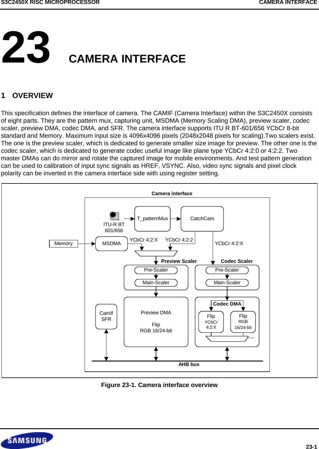
![CAMERA INTERFACE S3C2450X RISC MICROPROCESSOR 23-2 1.1 FEATURES • ITU-R BT 601/656 8-bit mode support • DZI (Digital Zoom In) capability • Programmable polarity of video sync signals • Max. 4096 x 4096 pixels input support (non-scaling) • Max. 2048 x 2048 pixels input support for codec scaling and 720 x 480 pixels input support for preview scaling • Image mirror and rotation (X-axis mirror, Y-axis mirror and 180° rotation) • Preview DMA output image generation (RGB 16/24-bit format) • Codec DMA output image generation (RGB 16/24-bit format or YCbCr 4:2:0/4:2:2 format) • Capture frame control support in codec_path • Scan line offset support in codec_path and preview_path • YCbCr 4:2:2 codec image format interleave support • MSDMA supports memory data for preview path input. • Image effect 2 EXTERNAL INTERFACE CAMIF can support the next video standards. • ITU-R BT 601 YCbCr 8-bit mode • ITU-R BT 656 YCbCr 8-bit mode 2.1 SIGNAL DESCRIPTION Table 23-1. Camera interface signal description Name I/O Active Description CAMPCLK I - Pixel Clock, driven by the Camera processor CAMVSYNC I H/L Frame Sync, driven by the Camera processor CAMHREF I H/L Horizontal Sync, driven by the Camera processor CAMDATA [7:0] I - Pixel Data driven by the Camera processor CAMCLKOUT O - Master Clock to the Camera processors CAMRESET O H/L Software Reset or Power Down for the Camera processor CAM_FIELD_A I - Interlace field (only used in interlace mode)](https://usermanual.wiki/Diasonic-Technology-Co/RVM-704M.Users-Manual/User-Guide-1826140-Page-626.png)
![S3C2450X RISC MICROPROCESSOR CAMERA INTERFACE 23-3 2.2 TIMING DIAGRAM VSYNCYCb YCr YCb YCb YCrHREFHREF (1H)PCLKDATA[7:0]Vertical linesHorizontal width1 frame8-bit mode Figure 23-2. ITU-R BT 601 Input Timing Diagram VSYNCFIELD Field 1 Field 2VSYNCFIELDFieldMode = 1 (Field port connects with FIELD) Figure 23-3. ITU-R BT 601 Interlace Timing Diagram PCLKDATA[7:0] CrFF 00 00 XY CbYFF 00 00 XYVideo timingreference codesPixel dataVideo timingreference codes Figure 23-4. ITU-R BT 656 Input Timing Diagram](https://usermanual.wiki/Diasonic-Technology-Co/RVM-704M.Users-Manual/User-Guide-1826140-Page-627.png)
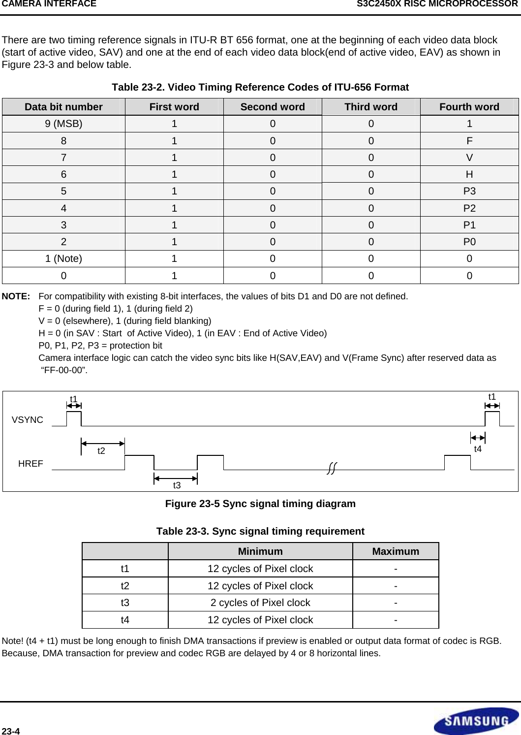
![S3C2450X RISC MICROPROCESSOR CAMERA INTERFACE 23-5 3 EXTERNAL/INTERNAL CONNECTION GUIDE All CAMIF input signals should not occur inter-skewing to pixel clock line. CAMRSTCAMCLKVSYNCHREFPCLKPDATA[7:0]CAMIFCamera ANo Skew Figure 23-6. IO Connection Guide 4 CAMERA INTERFACE OPERATION 4.1 TWO DMA PORTS CAMIF has two DMA port. P-port(Preview port) and C-port(Codec port) are separated from each other on AHB bus. At the view of system bus, two ports are independent. The P-port stores the RGB image data into memory for preview. The C-port stores the YCbCr 4:2:0 or 4:2:2 image data or RGB image data into memory for Codec as MPEG-4, H.263, etc. These two master ports support the variable applications like DSC (Digital Still Camera), MPEG-4 video conference, video recording, etc. For example, P-port image can be used as preview image, and C-port image can be used as JPEG image in DSC application. Also, the register setting can separately disable P-port or C-port.](https://usermanual.wiki/Diasonic-Technology-Co/RVM-704M.Users-Manual/User-Guide-1826140-Page-629.png)
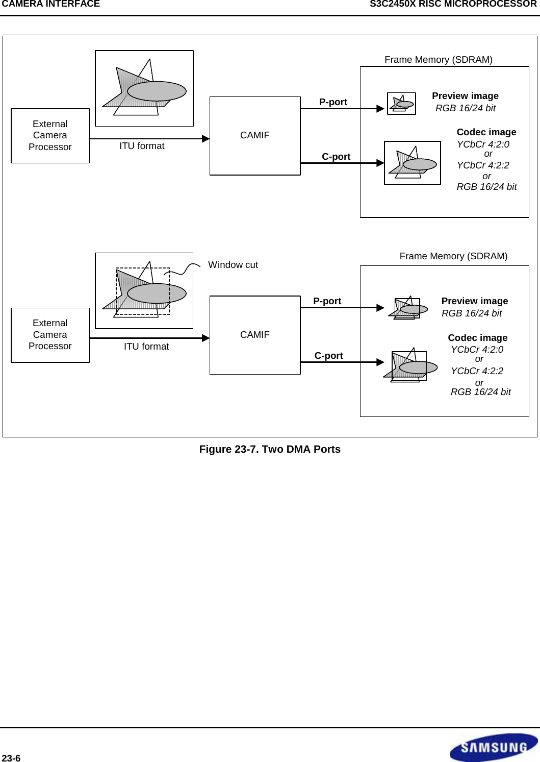
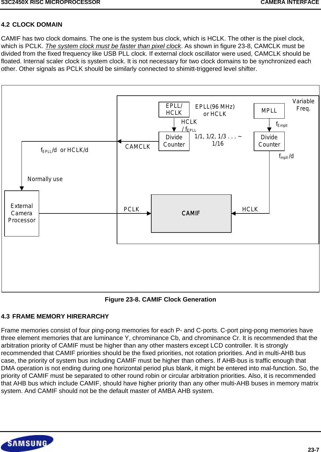
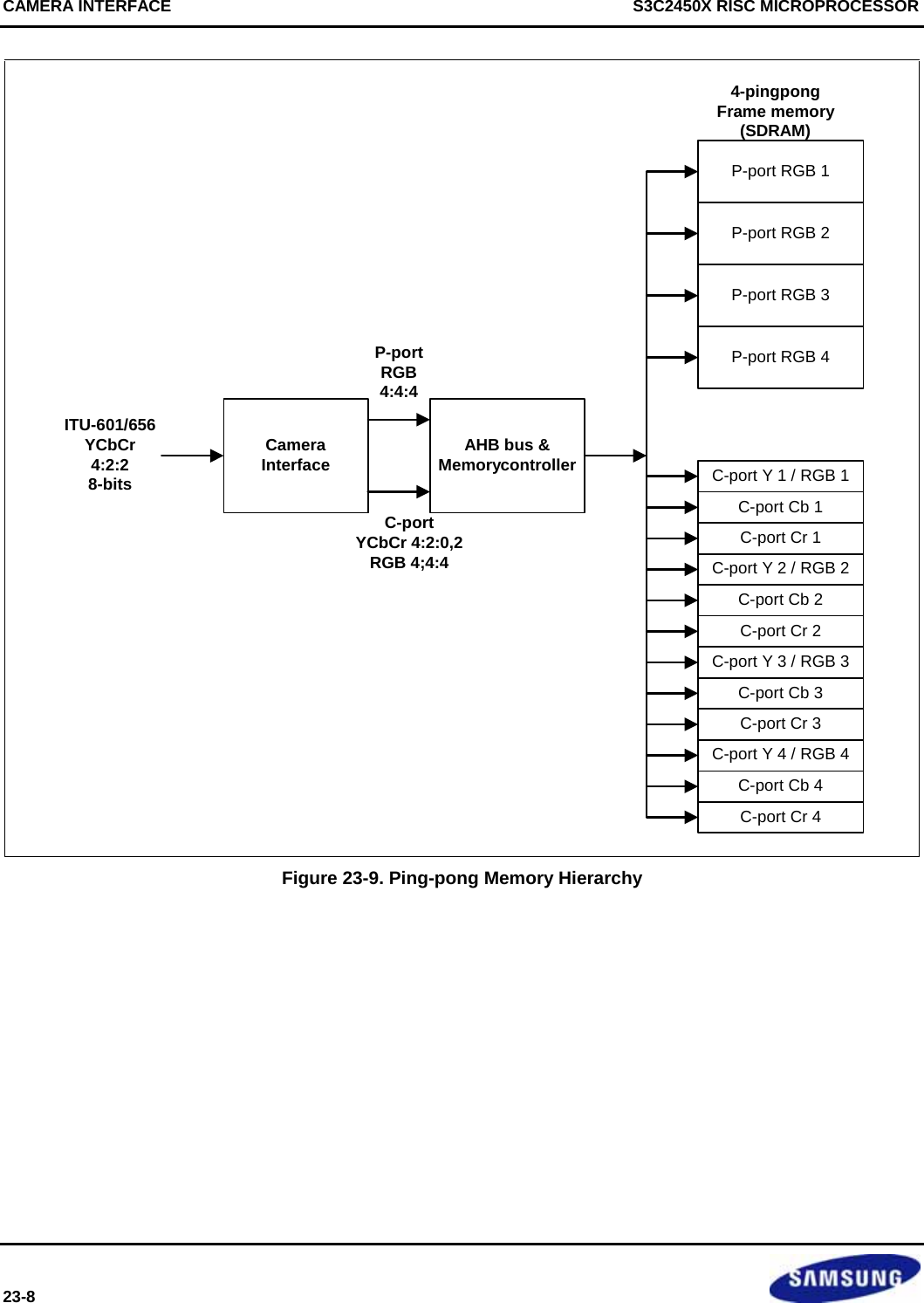
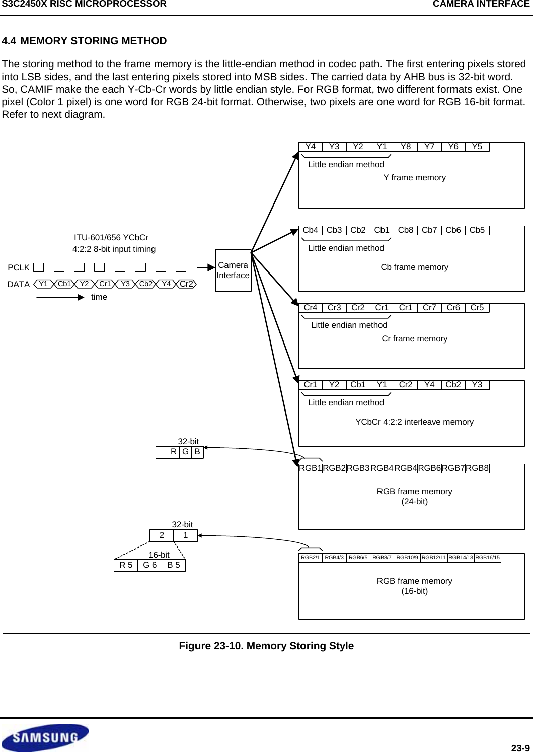

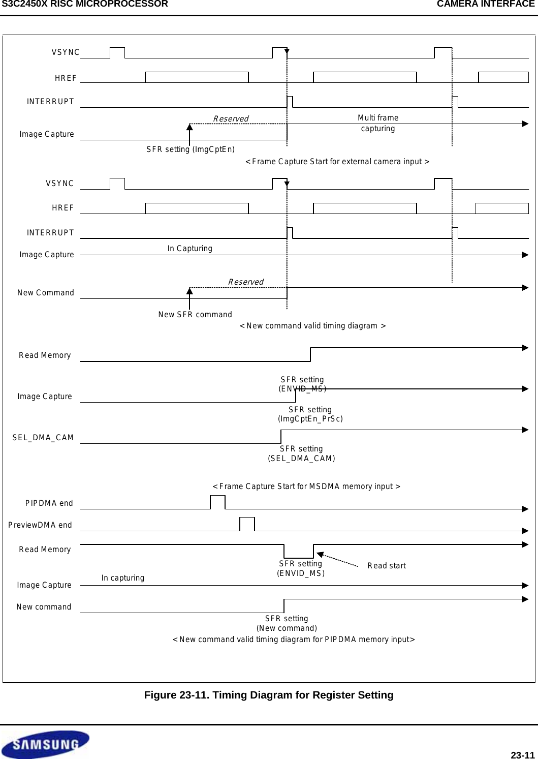
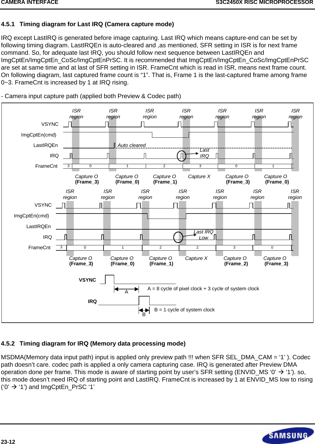
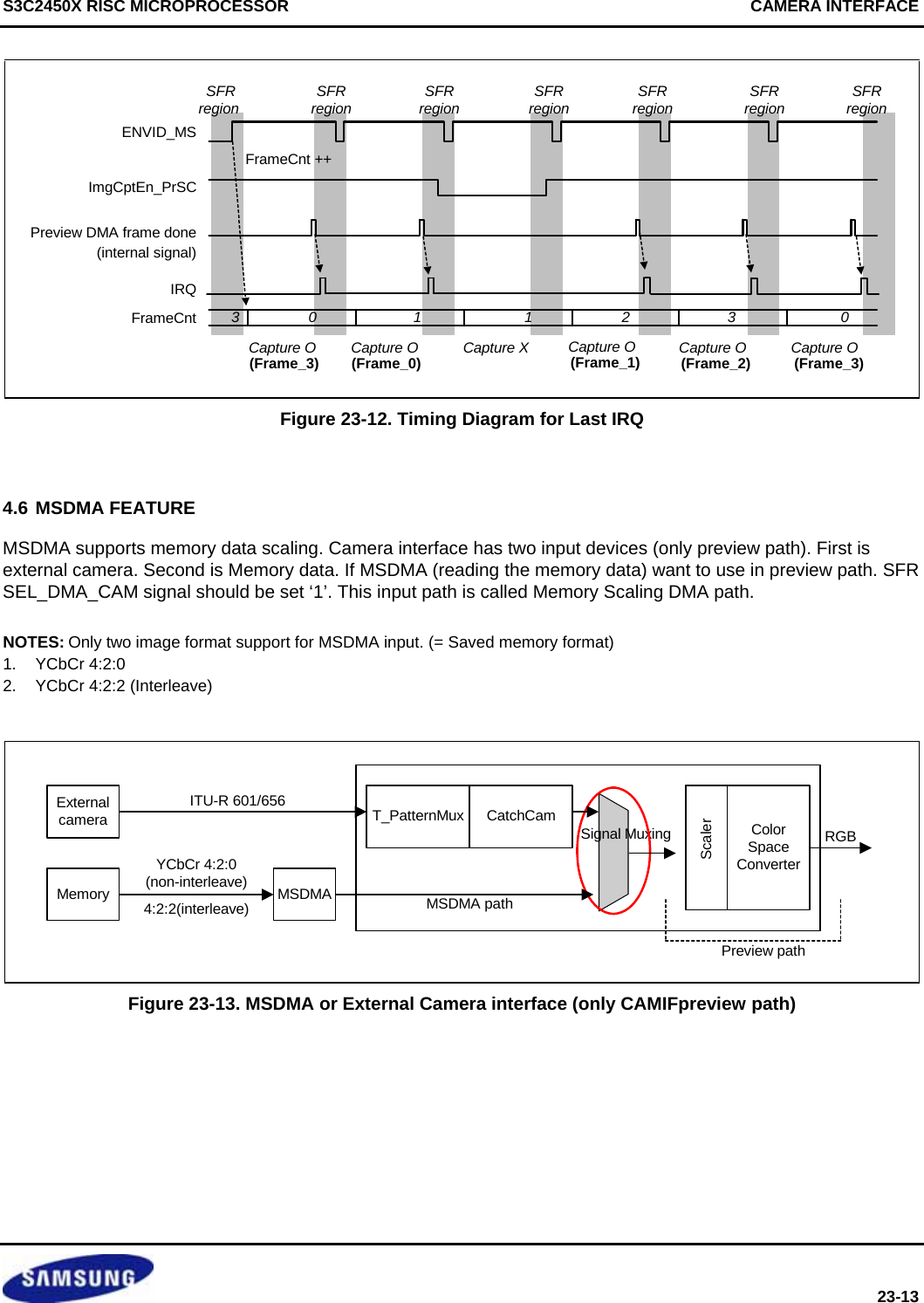
![CAMERA INTERFACE S3C2450X RISC MICROPROCESSOR 23-14 5 SOFTWARE INTERFACE CAMIF SFR (Special Function Register) 6 CAMERA INTERFACE SPECIAL REGISTERS • When preview input use MSDMA path, the first column mark (v) sfr will be related to the preview operation. • The last column means that each value can change by each VSYNC start during capture enable. (O : change , X : not change) 6.1 SOURCE FORMAT REGISTER Register Address R/W Description Reset ValueCISRCFMT 0x4D80_0000 RW Source format register 0 CISRCFMT Bit Description Initial State Change State ITU601_656n [31] 1 = ITU-R BT.601 YCbCr 8-bit mode enable 0 = ITU-R BT.656 YCbCr 8-bit mode enable 0 X UVOffset [30] Cb,Cr value offset control. 1 = +128 0 = +0 (normally used) 0 X In16bit [29] This bit must be 0. 0 X SourceHsize [28:16] Source horizontal pixel number (must be 8’s multiple) (Also, must be 4’s multiple of PreHorRatio if WinOfsEn is 0) 0 X Order422 [15:14] Input YCbCr order inform for input 8-bit mode 8-bit mode 00 : YCbYCr 01 : YCrYCb 10 : CbYCrY 11 : CrYCbY 0 X Reserved [13] 0 X SourceVsize [12:0] Source vertical pixel number. (Also, must be multiple of PreVerRatio when scale down if WinOfsEn is 0) 0 X](https://usermanual.wiki/Diasonic-Technology-Co/RVM-704M.Users-Manual/User-Guide-1826140-Page-638.png)
![S3C2450X RISC MICROPROCESSOR CAMERA INTERFACE 23-15 6.2 WINDOW OPTION REGISTER Register Address R/W Description Reset ValueCIWDOFST 0x4D80_0004 RW Window offset register 0 SourceHsizeOriginal InputWindow Cut: WinHorOfst,WinHorOfst2: WinVerOfst,WinVerOfst2TargetHsize_xxTargetHsize_xx= TargetHsize_Co orTargetHsize_Pr1 2343 41 2,,Source VsizeTargetVsize_xx Figure 23-14. Window Offset Scheme (WinHorOfst2 & WinVerOfst2 are assigned in the CIWDOFST2 register) CIWDOFST Bit Description Initial State Change State WinOfsEn [31] 1 = window offset enable 0 = no offset 0 O ClrOvCoFiY [30] 1 = clear the overflow indication flag of input CODEC FIFO Y 0 = normal 0 X Reserved [29:27] 0 X WinHorOfst [26:16] Window horizontal offset by pixel unit. (It should be 2’s multiple) Caution: SourceHsize-WinHorOfst- WinHorOfst2 should be 8’s multiple. 0 O ClrOvCoFiCb [15] 1 = clear the overflow indication flag of input CODEC FIFO Cb 0 = normal 0 X ClrOvCoFiCr [14] 1 = clear the overflow indication flag of input CODEC FIFO Cr 0 = normal 0 X ClrOvPrFiCb [13] 1 = clear the overflow indication flag of input PREVIEW FIFO Cb 0 = normal 0 X ClrOvPrFiCr [12] 1 = clear the overflow indication flag of input PREVIEW FIFO Cr 0 = normal 0 X Reserved [11] 0 X WinVerOfst [10:0] Window vertical offset by pixel unit 0 O](https://usermanual.wiki/Diasonic-Technology-Co/RVM-704M.Users-Manual/User-Guide-1826140-Page-639.png)
![S3C2450X RISC MICROPROCESSOR CAMERA INTERFACE 23-17 6.3 GLOBAL CONTROL REGISTER Register Address R/W Description Reset ValueCIGCTRL 0x4D80_0008 RW Global control register 2000_0000 CIGCTRL Bit Description Initial State Change State SwRst [31] Camera interface software reset. Before setting this bit, you should set the ITU601_656n bit of CISRCFMT as “1” temporarily at first SFR setting. Next sequence is recommended. (ITU601 case : ITU601_656n “1” → SwRst “1” → SwRst “0” for first SFR setting , ITU656 case : ITU601_656n “1” → SwRst “1” → SwRst “0” → ITU601_656n “0” for first SFR setting) 0 X CamRst [30] External camera processor Reset or Power Down control 0 X Reserved [29] Must be 1 1 X TestPattern [28:27] This register should be set at only ITU-T 601 8-bit mode. Not allowed with ITU-T 656 mode. (max. 1280 X 1024) 00 = external camera processor input (normal) 01 = color bar test pattern 10 = horizontal increment test pattern 11 = vertical increment test pattern 0 X InvPolPCLK [26] 1 = inverse the polarity of PCLK 0 = normal 0 X InvPolVSYNC [25] 1 = inverse the polarity of VSYNC 0 = normal 0 X InvPolHREF [24] 1 = inverse the polarity of HREF 0 = normal 0 X Non-use [23] 0 X IRQ_Ovfen [22] 1 = Overflow interrupt enable (Interrupt is generated during overflow occurrence) 0 = Overflow interrupt disable (normal) 0 X Href_mask [21] 1 = mask out Href during Vsync high 0 = no mask 0 X Reserved [20:0] 0 X FIELDMODE [2] ITU601 Interlace field port mode enable (don’t care this bit in itu656). This bit should be connected with FIELD signal 1 = FIELD port enable 0 = disable 0 X InvPolFIELD [1] 1 = inverse the polarity of FIELD 0 = normal 0 X Cam_Interlace [0] External camera data transmission mode 1 = Interlace 0 = Progressive 0 X](https://usermanual.wiki/Diasonic-Technology-Co/RVM-704M.Users-Manual/User-Guide-1826140-Page-641.png)
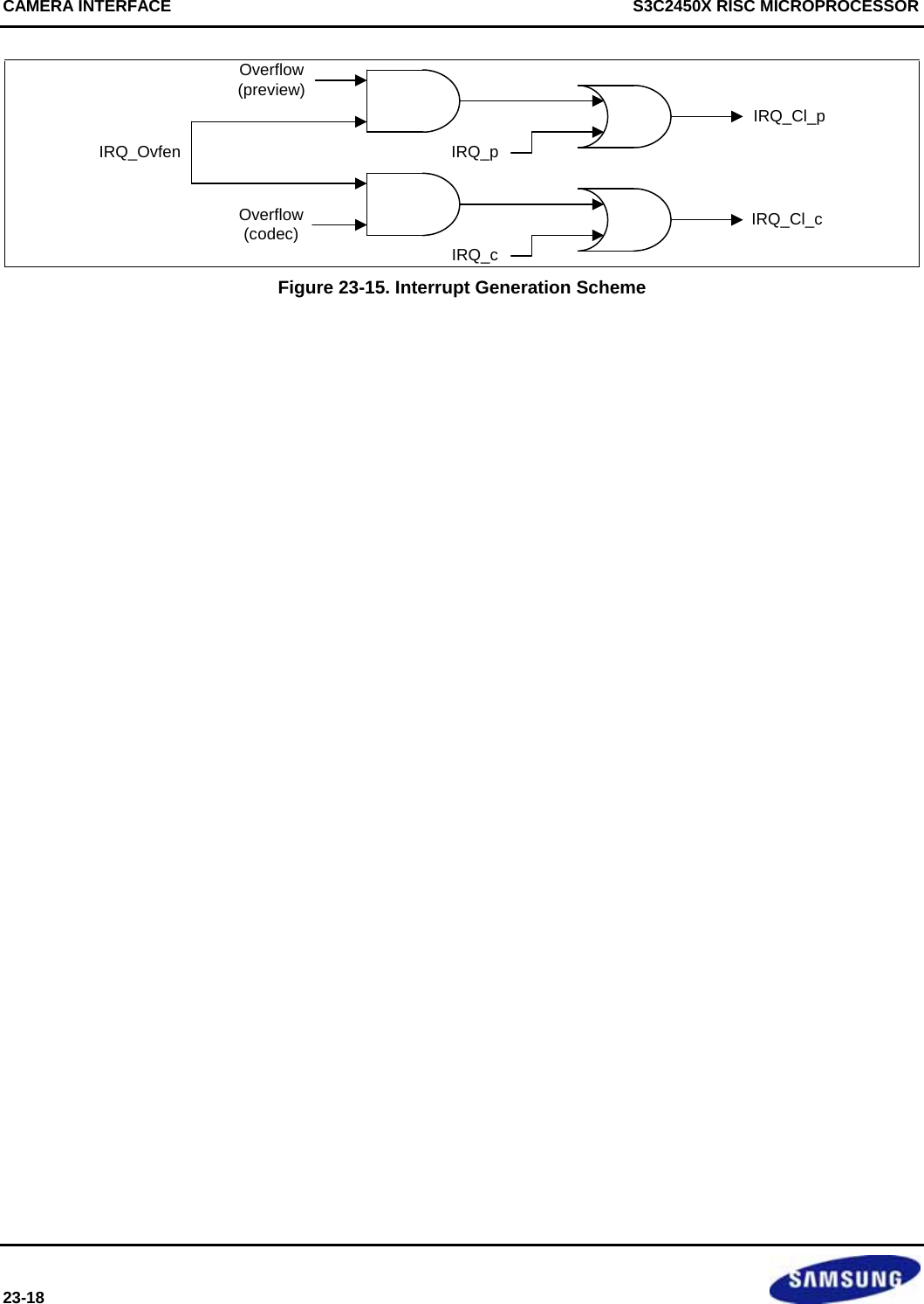
![S3C2450X RISC MICROPROCESSOR CAMERA INTERFACE 23-19 6.4 WINDOW OPTION REGISTER 2 Register Address R/W Description Reset ValueCIDOWSFT2 0x4D80_0014 RW Window offset register 2 0 CIWDOFST2 Bit Description Initial State Change State Reserved [31:27] 0 X WinHorOfst2 [26:16] Window horizontal offset2 by pixel unit. (It should be 2’s multiple) Caution : SourceHsize-WinHorOfst- WinHorOfst2 should be 8’s multiple. 0 O Reserved [15:11] 0 X WinVerOfst2 [10:0] Window vertical offset2 by pixel unit 0 O 6.5 Y1 START ADDRESS REGISTER Register Address R/W Description Reset ValueCICOYSA1 0x4D80_0018 RW 1st frame start address for codec DMA 0 CICOYSA1 Bit Description Initial State Change State CICOYSA1 [31:0] Output format : YCbCr 4:2:2 or 4:2:0 Æ Y 1st frame start address Output format : RGB 16/24 bit Æ RGB 1st frame start address 0 X 6.6 Y2 START ADDRESS REGISTER Register Address R/W Description Reset ValueCICOYSA2 0x4D80_001C RW 2nd frame start address for codec DMA 0 CICOYSA2 Bit Description Initial State Change State CICOYSA2 [31:0] Output format : YCbCr 4:2:2 or 4:2:0 Æ Y 2nd frame start address Output format : RGB 16/24 bit Æ RGB 2nd frame start address 0 X](https://usermanual.wiki/Diasonic-Technology-Co/RVM-704M.Users-Manual/User-Guide-1826140-Page-643.png)
![CAMERA INTERFACE S3C2450X RISC MICROPROCESSOR 23-20 6.7 Y3 START ADDRESS REGISTER Register Address R/W Description Reset ValueCICOYSA3 0x4D80_0020 RW 3rd frame start address for codec DMA 0 CICOYSA3 Bit Description Initial State Change State CICOYSA3 [31:0] Output format : YCbCr 4:2:2 or 4:2:0 Æ Y 3rd frame start address Output format : RGB 16/24 bit Æ RGB 3rd frame start address 0 X 6.8 Y4 START ADDRESS REGISTER Register Address R/W Description Reset ValueCICOYSA4 0x4D80_0024 RW 4th frame start address for codec DMA 0 CICOYSA4 Bit Description Initial State Change State CICOYSA4 [31:0] Output format : YCbCr 4:2:2 or 4:2:0 Æ Y 4th frame start address Output format : RGB 16/24 bit Æ RGB 4th frame start address 0 X 6.9 CB1 START ADDRESS REGISTER Register Address R/W Description Reset ValueCICOCBSA1 0x4D80_0028 RW Cb 1st frame start address for codec DMA 0 CICOCBSA1 Bit Description Initial State Change State CICOCBSA1 [31:0] Cb 1st frame start address for codec DMA 0 X](https://usermanual.wiki/Diasonic-Technology-Co/RVM-704M.Users-Manual/User-Guide-1826140-Page-644.png)
![S3C2450X RISC MICROPROCESSOR CAMERA INTERFACE 23-21 6.10 CB2 START ADDRESS REGISTER Register Address R/W Description Reset ValueCICOCBSA2 0x4D80_002C RW Cb 2nd frame start address for codec DMA 0 CICOCBSA2 Bit Description Initial State Change State CICOCBSA2 [31:0] Cb 2nd frame start address for codec DMA 0 X 6.11 CB3 START ADDRESS REGISTER Register Address R/W Description Reset ValueCICOCBSA3 0x4D80_0030 RW Cb 3rd frame start address for codec DMA 0 CICOCBSA3 Bit Description Initial State Change State CICOCBSA3 [31:0] Cb 3rd frame start address for codec DMA 0 X 6.12 CB4 START ADDRESS REGISTER Register Address R/W Description Reset ValueCICOCBSA4 0x4D80_0034 RW Cb 4th frame start address for codec DMA 0 CICOCBSA4 Bit Description Initial State Change State CICOCBSA4 [31:0] Cb 4th frame start address for codec DMA 0 X 6.13 CR1 START ADDRESS REGISTER Register Address R/W Description Reset ValueCICOCRSA1 0x4D80_0038 RW Cr 1st frame start address for codec DMA 0 CICOCRSA1 Bit Description Initial State Change State CICOCRSA1 [31:0] Cr 1st frame start address for codec DMA 0 X](https://usermanual.wiki/Diasonic-Technology-Co/RVM-704M.Users-Manual/User-Guide-1826140-Page-645.png)
![CAMERA INTERFACE S3C2450X RISC MICROPROCESSOR 23-22 6.14 CR2 START ADDRESS REGISTER Register Address R/W Description Reset ValueCICOCRSA2 0x4D80_003C RW Cr 2nd frame start address for codec DMA 0 CICOCRSA2 Bit Description Initial State Change State CICOCRSA2 [31:0] Cr 2nd frame start address for codec DMA 0 X 6.15 CR3 START ADDRESS REGISTER Register Address R/W Description Reset ValueCICOCRSA3 0x4D80_0040 RW Cr 3rd frame start address for codec DMA 0 CICOCRSA3 Bit Description Initial State Change State CICOCRSA3 [31:0] Cr 3rd frame start address for codec DMA 0 X 6.16 CR4 START ADDRESS REGISTER Register Address R/W Description Reset ValueCICOCRSA4 0x4D80_0044 RW Cr 4th frame start address for codec DMA 0 CICOCRSA4 Bit Description Initial State Change State CICOCRSA4 [31:0] Cr 4th frame start address for codec DMA 0 X](https://usermanual.wiki/Diasonic-Technology-Co/RVM-704M.Users-Manual/User-Guide-1826140-Page-646.png)
![S3C2450X RISC MICROPROCESSOR CAMERA INTERFACE 23-23 6.17 CODEC TARGET FORMAT REGISTER Register Address R/W Description Reset ValueCICOTRGFMT 0x4D80_0048 RW Target image format of codec DMA 0 CICOTRGFMT Bit Description Initial State Change State In422_Co [31] 1 = YCbCr 4:2:2 codec scaler input image format. 0 = YCbCr 4:2:0 codec scaler input image format. In this case, horizontal line decimation is performed before codec scaler. (normal) 0 O Out422_Co [30] 1 = YCbCr 4:2:2 codec scaler output image format. This mode is mainly for S/W JPEG. 0 = YCbCr 4:2:0 codec scaler output image format. This mode is mainly for MPEG-4 codec and H/W JPEG DCT.(normal) It must not be set to 0 when In422_Co is set to 0. 0 O Interleave_Co [29] 1 = Interleave ON (support image format YCbCr 4:2:2 only) Y0Cb0Y1Cr0Y2Cb1Y3Cr1…… 0 = Interleave OFF Y0Y1Y2Y3….Cb0Cb1….Cr0Cr1…. 0 O TargetHsize_Co [28:16] Horizontal pixel number of target image for codec DMA (16’s multiple) 0 X FlipMd_Co [15:14] Image mirror and rotation for codec DMA 00 = Normal 01 = X-axis mirror 10 = Y-axis mirror 11 = 180° rotation 0 O Reserved [13] 0 X TargetVsize_Co [12:0] Vertical pixel number of target image for codec DMA(8’s multiple when RGB mode is selected) 0 X TargetHsize_Co and TargetVsize_Co should not be larger than SourceHsize and SourceVsize. Caution! If TargetVsize_Co value is set to an odd number(N) and output format is YCbCr 4:2:0, The odd number(N) of Y lines and the (N-1)/2 of Cb, Cr lines are generated.](https://usermanual.wiki/Diasonic-Technology-Co/RVM-704M.Users-Manual/User-Guide-1826140-Page-647.png)
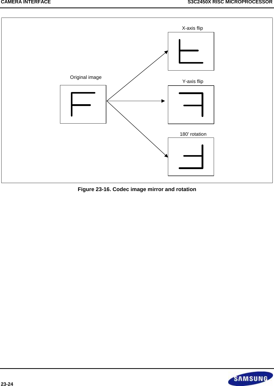
![S3C2450X RISC MICROPROCESSOR CAMERA INTERFACE 23-25 6.18 CODEC DMA CONTROL REGISTER Register Address R/W Description Reset ValueCICOCTRL 0x4D80_004C RW Codec DMA control related 0 CICOCTRL Bit Description Initial State Change State Reserved [31:24] 0 X Yburst1_Co [23:19] Output format : YCbCr Æ Main burst length for codec Y frames Output format : RGB Æ Main burst length for RGB frame 0 X Yburst2_Co [18:14] Output format : YCbCr Æ Remained burst length for codec Y frames Output format : RGB Æ Remained burst length for RGB frame 0 X Cburst1_Co [13:9] Main burst length for codec Cb/Cr frames 0 X Cburst2_Co [8:4] Remained burst length for codec Cb/Cr frames 0 X Reserved [3] 0 X LastIRQEn_Co [2] 1 = enable last IRQ at the end of frame capture (It is recommended to check the done signal of capturing image for JPEG. One pulse) 0 = normal 0 X Order422_Co [1:0] Interleaved YCbCr 4:2:2 output order memory storing style LSB MSB 00 Y0Cb0Y1Cr0 01 Y0Cr0Y1Cb0 10 Cb0Y0Cr0Y1 11 Cr0Y0Cb0Y1 0 X • Interleaved burst length Y burst length 2 , 4 , 8 C burst length (C burst length = Y burst length / 2) 1 , 2 , 4 Wanted burst length ( = Y + 2C ) 4 , 8 , 16 NOTE: When Codec output format is YCbCr 4:2:2 interleave ,ScalerBypass_Co = 0 and ScaleUp_V_Co = 1 , Wanted main burst length = 16 and Wanted remained burst length ≠ 16 is not allowed.](https://usermanual.wiki/Diasonic-Technology-Co/RVM-704M.Users-Manual/User-Guide-1826140-Page-649.png)
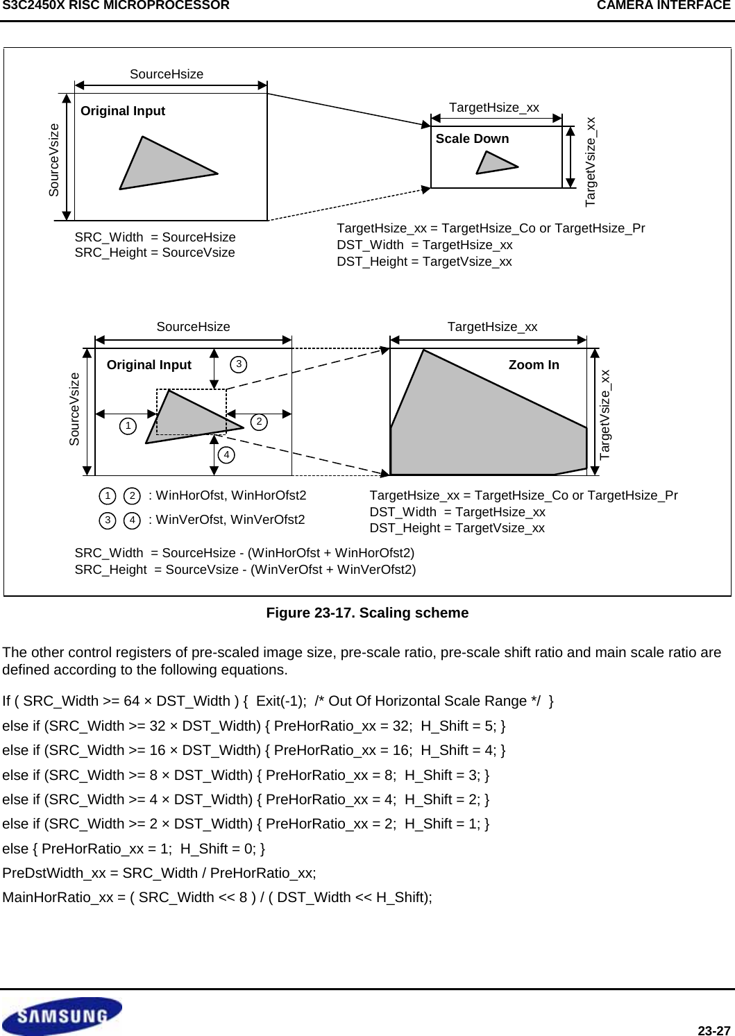
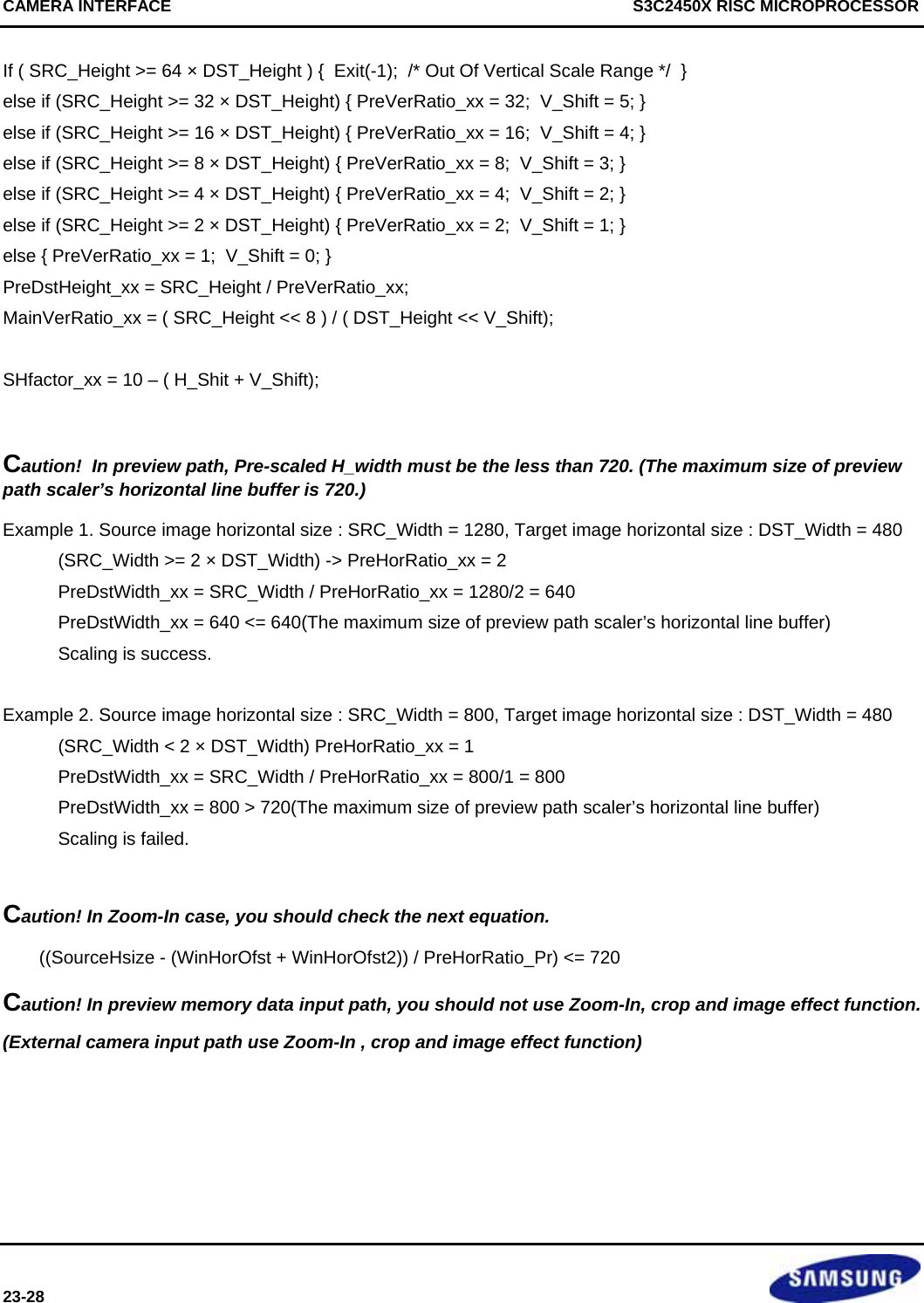
![S3C2450X RISC MICROPROCESSOR CAMERA INTERFACE 23-29 6.20 CODEC PRE-SCALER CONTROL REGISTER 1 Register Address R/W Description Reset ValueCICOSCPRERATIO 0x4D80_0050 RW Codec pre-scaler ratio control 0 CICOSCPRERATIO Bit Description Initial State Change State SHfactor_Co [31:28] Shift factor for codec pre-scaler 0 O Reserved [27:23] 0 X PreHorRatio_Co [22:16] Horizontal ratio of codec pre-scaler 0 O Reserved [15:7] 0 X PreVerRatio_Co [6:0] Vertical ratio of codec pre-scaler 0 O 6.21 CODEC PRE-SCALER CONTROL REGISTER 2 Register Address R/W Description Reset ValueCICOSCPREDST 0x4D80_0054 RW Codec pre-scaler destination format 0 CICOSCPREDST Bit Description Initial State Change State Reserved [31:28] 0 X PreDstWidth_Co [27:16] Destination width for codec pre-scaler 0 O Reserved [15:12] 0 X Reserved [31:28] 0 X PreDstHeight_Co [11:0] Destination height for codec pre-scaler 0 O](https://usermanual.wiki/Diasonic-Technology-Co/RVM-704M.Users-Manual/User-Guide-1826140-Page-653.png)
![CAMERA INTERFACE S3C2450X RISC MICROPROCESSOR 23-30 6.22 CODEC MAIN-SCALER CONTROL REGISTER Register Address R/W Description Reset ValueCICOSCCTRL 0x4D80_0058 RW Codec main-scaler control 0 CICOSCCTRL Bit Description Initial State Change State ScalerBypass_Co [31] Codec scaler bypass for upper 2048 x 2048 size (In this case, ImgCptEn_CoSC and ImgCptEn_PrSC should be 0, but ImgCptEn should be 1. It is not allowed to capturing preview image. This mode is intended to capture JPEG input image for DSC application) In this case, input pixel buffering depends on only input FIFOs, so system bus should be not busy in this mode. 0 O ScaleUp_H_Co [30] Horizontal scale up/down flag for codec scaler (In 1:1 scale ratio, this bit should be “1”) 1: up, 0:down 0 O ScaleUp_V_Co [29] Vertical scale up/down flag for codec scaler (In 1:1 scale ratio, this bit should be “1”) 1: up, 0:down 0 O Reserved [28:25] 0 X MainHorRatio_Co [24:16] Horizontal scale ratio for codec main-scaler 0 O CoScalerStart [15] Codec scaler start 0 O Reserved [14:9] 0 X MainVerRatio_Co [8:0] Vertical scale ratio for codec main-scaler 0 O 6.23 CODEC DMA TARGET AREA REGISTER Register Address R/W Description Reset ValueCICOTAREA 0x4D80_005C RW Codec pre-scaler destination format 0 CICOTAREA Bit Description Initial State Change State Reserved [31:26] 0 X CICOTAREA [25:0] Target area for codec DMA = Target H size x Target V size 0 X](https://usermanual.wiki/Diasonic-Technology-Co/RVM-704M.Users-Manual/User-Guide-1826140-Page-654.png)
![S3C2450X RISC MICROPROCESSOR CAMERA INTERFACE 23-31 6.24 CODEC STATUS REGISTER Register Address R/W Description Reset ValueCICOSTATUS 0x4D80_0064 R Codec path status 0 CICOSTATUS Bit Description Initial State Change State OvFiY_Co [31] Overflow state of codec FIFO Y 0 X OvFiCb_Co [30] Overflow state of codec FIFO Cb 0 X OvFiCr_Co [29] Overflow state of codec FIFO Cr 0 X VSYNC [28] Camera VSYNC (This bit can be referred by CPU for first SFR setting after external camera muxing. And, it can be seen in the ITU-R BT 656 mode) 0 X FrameCnt_Co [27:26] Frame count of codec DMA (This counter value means the next frame number) 0 X WinOfstEn_Co [25] Window offset enable status 0 X FlipMd_Co [24:23] Flip mode of codec DMA 0 X ImgCptEn_ CamIf [22] Image capture enable of camera interface 0 X ImgCptEn_ CoSC [21] Image capture enable of codec path 0 X VSYNC [20] External camera VSYNC (polarity inversion was not adopted.) X X Reserved [9:1] Reserved 0 X FIELD [0] Camera FIELD(polarity inversion was adopted) 0 X 6.25 RGB1 START ADDRESS REGISTER Register Address R/W Description Reset ValueCIPRCLRSA1 0x4D80_006C RW RGB 1st frame start address for preview DMA 0 CIPRCLRSA1 Bit Description Initial State Change State CIPRCLRSA1 (v) [31:0] RGB 1st frame start address for preview DMA 0 X](https://usermanual.wiki/Diasonic-Technology-Co/RVM-704M.Users-Manual/User-Guide-1826140-Page-655.png)
![CAMERA INTERFACE S3C2450X RISC MICROPROCESSOR 23-32 6.26 RGB2 START ADDRESS REGISTER Register Address R/W Description Reset ValueCIPRCLRSA2 0x4D80_0070 RW RGB 2nd frame start address for preview DMA 0 CIPRCLRSA2 Bit Description Initial State Change State CIPRCLRSA2 (v) [31:0] RGB 2nd frame start address for preview DMA 0 X 6.27 RGB3 START ADDRESS REGISTER Register Address R/W Description Reset ValueCIPRCLRSA3 0x4D80_0074 RW RGB 3rd frame start address for preview DMA 0 CIPRCLRSA3 Bit Description Initial State Change State CIPRCLRSA3 (v) [31:0] RGB 3rd frame start address for preview DMA 0 X 6.28 RGB4 START ADDRESS REGISTER Register Address R/W Description Reset ValueCIPRCLRSA4 0x4D80_0078 RW RGB 4th frame start address for preview DMA 0 CIPRCLRSA4 Bit Description Initial State Change State CIPRCLRSA4 (v) [31:0] RGB 4th frame start address for preview DMA 0 X](https://usermanual.wiki/Diasonic-Technology-Co/RVM-704M.Users-Manual/User-Guide-1826140-Page-656.png)
![S3C2450X RISC MICROPROCESSOR CAMERA INTERFACE 23-33 6.29 PREVIEW TARGET FORMAT REGISTER Register Address R/W Description Reset ValueCIPRTRGFMT 0x4D80_007C RW Target image format of preview DMA 0x8000_0000 Original imageX-axis flipY-axis flip180' rotation Figure 23-18. Preview Image Mirror and Rotation CIPRTRGFMT Bit Description Initial State Change State CSCRange (v) [31:30] YCbCr Input Data Dynamic Range Selection for the Color Space Conversion 2’b11 = Forbidden 2’b10 = 0 < Y/Cb/Cr <255 (Recommended) 2’b01 = 16 <= Y <= 235, 16 <= Cb/Cr <= 240 2’b00 = Reserved 2’b10 O Reserved [29] 0 X TargetHsize_Pr (v) [28:16] Horizontal pixel number of target image for preview DMA 16bppRGB:4n(n=1,2,3,…) 24bpp RGB : 2n(n=1,2,3, …) 0 X FlipMd_Pr (v) [15:14] Image mirror and rotation for preview DMA 00 = normal 01 = x-axis mirror 10 = y-axis mirror 11 = 180° rotation 0 O Reserved [13] 0 X TargetVsize_Pr (v) [12:0] Vertical pixel number of target image for preview DMA (8’s multiple) 0 X TargetHsize_Pr and TargetVsize_Pr should not be larger than SourceHsize and SourceVsize.](https://usermanual.wiki/Diasonic-Technology-Co/RVM-704M.Users-Manual/User-Guide-1826140-Page-657.png)
![CAMERA INTERFACE S3C2450X RISC MICROPROCESSOR 23-34 6.30 PREVIEW DMA CONTROL REGISTER Register Address R/W Description Reset Value CIPRCTRL 0x4D80_0080 RW Preview DMA control related 0 CIPRCTRL Bit Description Initial State Change State Reserved [31:24] 0 X RGBburst1_Pr (v) [23:19] Main burst length for preview RGB frames 0 X RGBburst2_Pr (v) [18:14] Remained burst length for preview RGB frames 0 X Reserved [13:3] 0 X LastIRQEn_Pr (v) [2] 1 : enable last IRQ at the end of frame capture (One pulse) 0 : normal 0 X Reserved [1:0] 0 X Main burst lengths must be one of the 4,8,16 and Remained burst lengths must be one of the 2,4,8,16. Example 1. Target image size : QCIF for RGB 32-bit format (horizontal width = 176 pixels. 1 pixel = 1 word) 176 pixel = 176 word. 176 % 16 = 0 Æ main burst = 16, remained burst = 16 Example 2. Target image size : VGA for RGB 16-bit format (horizontal width = 640 pixels. 2 pixel = 1 word) 640 / 2 = 320 word. 320 % 16 = 0 Æ main burst = 16, remained burst = 16](https://usermanual.wiki/Diasonic-Technology-Co/RVM-704M.Users-Manual/User-Guide-1826140-Page-658.png)
![S3C2450X RISC MICROPROCESSOR CAMERA INTERFACE 23-35 6.31 PREVIEW PRE-SCALER CONTROL REGISTER 1 Register Address R/W Description Reset ValueCIPRSCPRE RATIO 0x4D80_0084 RW Preview pre-scaler ratio control 0 CIPRSC PRERATIO Bit Description Initial State Change State SHfactor_Pr (v) [31:28] Shift factor for preview pre-scaler 0 O Reserved [27:23] 0 X PreHorRatio_Pr (v) [22:16] Horizontal ratio of preview pre-scaler 0 O Reserved [15:7] 0 X PreVerRatio_Pr (v) [6:0] Vertical ratio of preview pre-scaler 0 O 6.32 PREVIEW PRE-SCALER CONTROL REGISTER 2 Register Address R/W Description Reset ValueCIPRSC PREDST 0x4D80_0088 RW Preview pre-scaler destination format 0 CIPRSC PREDST Bit Description Initial State Change State Reserved [31:28] 0 X PreDstWidth_ Pr (v) [27:16] Destination width for preview pre-scaler 0 O Reserved [15:12] 0 X PreDstHeight_ Pr (v) [11:0] Destination height for preview pre-scaler 0 O](https://usermanual.wiki/Diasonic-Technology-Co/RVM-704M.Users-Manual/User-Guide-1826140-Page-659.png)
![CAMERA INTERFACE S3C2450X RISC MICROPROCESSOR 23-36 6.33 PREVIEW MAIN-SCALER CONTROL REGISTER Register Address R/W Description Reset ValueCIPRSCCTRL 0x4D80_008C RW Preview main-scaler control 0 CIPRSCCTRL Bit Description Initial State Change State Sample_Pr (v) [31] Sampling method for format conversion. (normally 1) 0 O RGBformat_Pr (v) [30] 1 = 24-bit RGB 0 = 16-bit RGB 0 O ScaleUp_H_Pr (v) [29] Horizontal scale up/down flag for preview scaler (In 1:1 scale ratio, this bit should be “1”) 1 = up 0 = down 0 O ScaleUp_V_Pr (v) [28] Vertical scale up/down flag for preview scaler (In 1:1 scale ratio, this bit should be “1”) 1 = up 0 = down 0 O Reserved [27:25] 0 X MainHorRatio_ Pr (v) [24:16] Horizontal scale ratio for preview main-scaler 0 O PrScalerStart (v) [15] Preview scaler start 0 O Reserved [14:9] 0 X MainVerRatio_ Pr (v) [8:0] Vertical scale ratio for preview main-scaler 0 O 6.34 PREVIEW DMA TARGET AREA REGISTER Register Address R/W Description Reset ValueCIPRTAREA 0x4D80_0090 RW Preview pre-scaler destination format 0 CIPRTAREA Bit Description Initial State Change State Reserved [31:26] 0 X CIPRTAREA (v) [25:0] Target area for preview DMA = Target H size x Target V size 0 X](https://usermanual.wiki/Diasonic-Technology-Co/RVM-704M.Users-Manual/User-Guide-1826140-Page-660.png)
![S3C2450X RISC MICROPROCESSOR CAMERA INTERFACE 23-37 6.35 PREVIEW STATUS REGISTER Register Address R/W Description Reset ValueCIPRSTATUS 0x4D80_0098 R Preview path status 0 CIPRSTATUS Bit Description Initial State Change State OvFiCb_Pr [31] Overflow state of preview FIFO Cb 0 X OvFiCr_Pr [30] Overflow state of preview FIFO Cr 0 X Reserved [29:28] 0 X FrameCnt_Pr [27:26] Frame count of preview DMA 0 X Reserved [25] 0 X FlipMd_Pr [24:23] Flip mode of preview DMA 0 X Reserved [22] 0 X ImgCptEn_ PrSC [21] Image capture enable of preview path 0 X Reserved [20:0] 0 X](https://usermanual.wiki/Diasonic-Technology-Co/RVM-704M.Users-Manual/User-Guide-1826140-Page-661.png)
![CAMERA INTERFACE S3C2450X RISC MICROPROCESSOR 23-38 6.36 IMAGE CAPTURE ENABLE REGISTER Register Address R/W Description Reset ValueCIIMGCPT 0x4D80_00A0 RW Image capture enable command 0 CIIMGCPT Bit Description Initial State Change State ImgCptEn [31] camera interface global capture enable 0 O ImgCptEn_ CoSc [30] capture enable for codec scaler. This bit must be zero in scaler-bypass mode. 0 O ImgCptEn_ PrSc (v) [29] capture enable for preview scaler. (applied both Memory data input path and External camera path in using preview) This bit must be zero in scaler-bypass mode. 0 O Reserved [28:27] 0 X Cpt_CoDMA_ Sel [26] Codec DMA output format 1 = RGB 16/24 bit (Must be Out422_Co=1 , Interleave_Co=1) 0 = YCbCr 4:2:2 or 4:2:0 0 O Cpt_CoDMA_ RGBFMT [25] Codec DMA RGB format 1 = RGB 24-bit 0 = RGB 16-bit 0 O Cpt_CoDMA_ En [24] Capture codec dma frame control. It is also used for start signal of Codec image capture. Therefore, it must be set to ‘1’ if codec image is wanted. or it must be set to ‘0’ if codec image is not captured. 1 = Enable 0 Disable 0 X Cpt_CoDMA_ Ptr [23:19] Capture sequence turn-around pointer 0 X Cpt_CoDMA_ Mod [18] Capture codec dma mode 1 = Apply Cpt_CoDMA_Cnt mode (capture Cpt_CoDMA_Cnt frames along the Cpt_CoDMA_Seq after Cpt_CoDMA_En becomes high) 0 = Apply Cpt_CoDMA_En mode (capture frames along the Cpt_CoDMA_Seq during Cpt_CoDMA_En is high) 0 X Cpt_CoDMA_ Cnt [17:10] Wanted number of frames to be captured (when read, you will see the value of a shadow register which is downcounted when a frame is captured. That is, Cpt_CoDMA_Cnt has an initially loaded value still after a frame is captured.) 0 X Reserved [9:0] 0 X](https://usermanual.wiki/Diasonic-Technology-Co/RVM-704M.Users-Manual/User-Guide-1826140-Page-662.png)
![S3C2450X RISC MICROPROCESSOR CAMERA INTERFACE 23-39 6.37 CODEC CAPTURE SEQUENCE REGISTER Register Address R/W Description Reset Value CICOCPTSEQ 0x4D80_00A4 RW Codec DMA capture sequence related 0xFFFFFFFF CICOCPTSEQ Bit Description Initial State Cpt_CoDMA_Seq [31:0] Capture sequence pattern in Codec DMA 0xFFFF_FFFF Cpt_CoDMA_Ptr31 30 29 10Cpt_CoDMA_Seq[31:0]RepeatCapture Capture NoCapture Capture1 1 1. . . . . . 0 10 Figure 23-19. Capture codec dma frame control • For skipped frmes, IRQ_CI_c is not generated. And FrameCnt_co is not increased](https://usermanual.wiki/Diasonic-Technology-Co/RVM-704M.Users-Manual/User-Guide-1826140-Page-663.png)
![CAMERA INTERFACE S3C2450X RISC MICROPROCESSOR 23-40 6.38 CODEC SCAN LINE OFFSET REGISTER Register Address R/W Description Reset ValueCICOSCYOS 0x4D80_00A8 RW Codec scan line Y offset related 0 CICOSCYOS Bit Description Initial State Change State Reserved [31:29] 0 X Initial_Yoffset_Co [28:16] The number of the skipped pixels for initial offset (should be even number for word boundary alignment). This value must be set to 0 when scanline offset is not used. And, scanline offset can be used only when Interleave_Co is set to 1. 0 O Reserved [15:13] 0 X Line_Yoffset_Co [12:0] The number of the skipped pixels in the screen of the target image when scan line is changed (should be even number for word boundary alignment). This value must be set to 0 when scanline offset is not used. And, scanline offset can be used only when Interleave_Co is set to 1. 0 O 6.39 PREVIEW SCAN LINE OFFSET REGISTER Register Address R/W Description Reset ValueCIPRSCOS 0x4D80_00AC RW Preview scan line offset related 0 CIPRSCOS Bit Description Initial State Change State Reserved [31:29] 0 X Initial_offset_Pr [28:16] The number of the skipped pixels for initial offset (should be even number for word boundary alignment). This value must be set to 0 when scanline offset is not used. 0 O Reserved [15:13] 0 X Line_offset_Pr [12:0] The number of the skipped pixels in the screen of the target image when scan line is changed (should be even number for word boundary alignment). This value must be set to 0 when scanline offset is not used. 0 O • Scan line offset is allowed all output format.](https://usermanual.wiki/Diasonic-Technology-Co/RVM-704M.Users-Manual/User-Guide-1826140-Page-664.png)
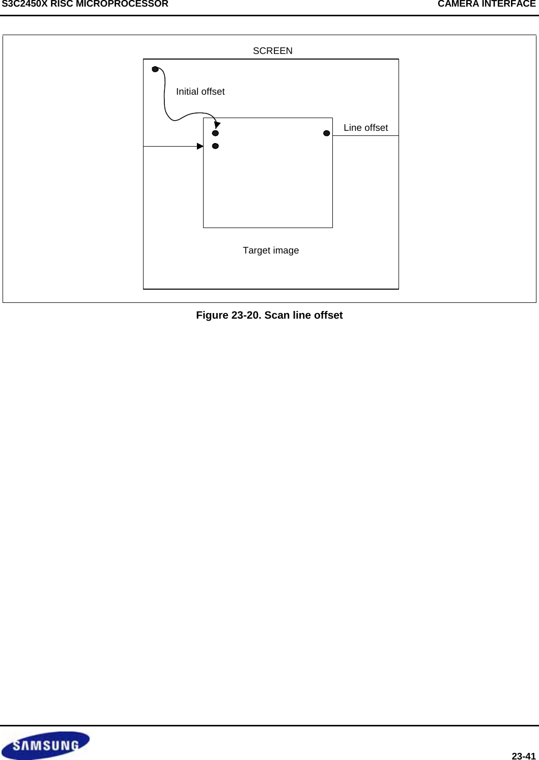
![CAMERA INTERFACE S3C2450X RISC MICROPROCESSOR 23-42 6.40 IMAGE EFFECTS REGISTER Register Address R/W Description Reset ValueCIIMGEFF 0x4D80_00B0 RW Image Effects related 0010_0080 CIIMGEFF Bit Description Initial State Change State Reserved [31:29] 0 X FIN [28:26] Image Effect selection 3’b000 : Bypass 3’b001 : Arbitrary Cb/Cr 3’b010 : Negative 3’b011 : Art Freeze 3’b100 : Embossing 3’b101 : Silhouette 0 O Reserved [25:21] 0 X PAT_Cb [20:13] It is used only for FIN is Arbitrary Cb/Cr ( PAT_Cb/Cr == 8’d128 for GRAYSCALE) 16 ≤ PAT_Cb ≤ 223 8’d128 O Reserved [12:8] 0 X PAT_Cr [7:0] It is used only for FIN is Arbitrary Cb/Cr ( PAT_Cb/Cr == 8’d128 for GRAYSCALE) 16 ≤ PAT_Cr ≤ 223 8’d128 O Cf) sepia : PAT_Cb == 8’d115 , PAT_Cr == 8’d145 Original Arbitrary(sepia) Negative Art freeze Embossing Silhouette Figure 23-21. Image Effect Result](https://usermanual.wiki/Diasonic-Technology-Co/RVM-704M.Users-Manual/User-Guide-1826140-Page-666.png)
![S3C2450X RISC MICROPROCESSOR CAMERA INTERFACE 23-43 6.41 MSDMA Y START ADDRESS REGISTER Register Address R/W Description Reset ValueCIMSYSA 0x4D80_00B4 RW MSDMA Y start address related 0000_0000 CIMSYSA Bit Description Initial State Change State Reserved [31] 0 X CIMSYSA (v) [30:0] DMA start address for Y component (YCbCr 4:2:0) DMA start address for YCbCr component (interleave 4:2:2) 0 X 6.42 MSDMA CB START ADDRESS REGISTER Register Address R/W Description Reset ValueCIMSCBSA 0x4D80_00B8 RW MSDMA Cb start address related 0000_0000 CIMSCBSA Bit Description Initial State Change State Reserved [31] 0 X CIMSCBSA (v) [30:0] DMA start address for Cb component (YCbCr 4:2:0) 0 X 6.43 MSDMA CR START ADDRESS REGISTER Register Address R/W Description Reset ValueCIMSCRSA 0x4D80_00BC RW MSDMA Cr start address related 0000_0000 CIMSCRSA Bit Description Initial State Change State Reserved [31] 0 X CIMSCRSA (v) [30:0] DMA start address for Cr component (YCbCr 4:2:0) 0 X](https://usermanual.wiki/Diasonic-Technology-Co/RVM-704M.Users-Manual/User-Guide-1826140-Page-667.png)
![CAMERA INTERFACE S3C2450X RISC MICROPROCESSOR 23-44 6.44 MSDMA Y END ADDRESS REGISTER Register Address R/W Description Reset ValueCIMSYEND 0x4D80_00C0 RW MSDMA Y end address related 0000_0000 CIMSYEND Bit Description Initial State Change State Reserved [31] 0 X CIMSYEND (v) [30:0] DMA End address for Y component (YCbCr 4:2:0) DMA End address for YCbCr component (interleave 4:2:2) 0 X 6.45 MSDMA CB END ADDRESS REGISTER Register Address R/W Description Reset ValueCIMSCBEND 0x4D80_00C4 RW MSDMA Cb end address related 0000_0000 CIMSCBEND Bit Description Initial State Change State Reserved [31] 0 X CIMSCBEND (v) [30:0] DMA End address for Cb component (YCbCr 4:2:0) 0 X 6.46 MSDMA CR END ADDRESS REGISTER Register Address R/W Description Reset ValueCIMSCREND 0x4D80_00C8 RW MSDMA Cr end address related 0000_0000 CIMSCREND Bit Description Initial State Change State Reserved [31] 0 X CIMSCREND (v) [30:0] DMA End address for Cr component (YCbCr 4:2:0) 0 X](https://usermanual.wiki/Diasonic-Technology-Co/RVM-704M.Users-Manual/User-Guide-1826140-Page-668.png)
![S3C2450X RISC MICROPROCESSOR CAMERA INTERFACE 23-45 6.47 MSDMA Y OFFSET REGISTER Register Address R/W Description Reset ValueCIMSYOFF 0x4D80_00CC RW MSDMA Y offset related 0000_0000 CIMSYOFF Bit Description Initial State Change State Reserved [31:24] 0 X CIMSYOFF (v) [23:0] Offset of Y component for fetching source image 0 X 6.48 MSDMA CB OFFSET REGISTER Register Address R/W Description Reset ValueCIMSCBOFF 0x4D80_00D0 RW MSDMA Cb offset related 0000_0000 CIMSCBOFF Bit Description Initial State Change State Reserved [31:24] 0 X CIMSCBOFF (v) [23:0] Offset of Cb component for fetching source image 0 X 6.49 MSDMA CR OFFSET REGISTER Register Address R/W Description Reset ValueCIMSCROFF 0x4D80_00D4 RW MSDMA Cr offset related 0000_0000 CIMSCROFF Bit Description Initial State Change State Reserved [31:24] 0 X CIMSCROFF (v) [23:0] Offset of Cr component for fetching source image 0 X 6.50 MSDMA SOURCE IMAGE WIDTH REGISTER Register Address R/W Description Reset ValueCIMSWIDTH 0x4D80_00D8 RW MSDMA source image width related 0000_0000 CIMSWIDTH Bit Description Initial State Change State Reserved [31:12] 0 X CIMSWIDTH (v) [11:0] MSDMA source image horizontal pixel size (must be 8’s multiple. It must be 4’s multiple of PreHorRatio. minimum 16) 0 X](https://usermanual.wiki/Diasonic-Technology-Co/RVM-704M.Users-Manual/User-Guide-1826140-Page-669.png)
![CAMERA INTERFACE S3C2450X RISC MICROPROCESSOR 23-46 6.50.1 - MSDMA Start address Start address of ADDRStart_Y/Cb/Cr points the first word address where the corresponding component of Y/Cb/Cr is read. Each one should be aligned with word boundary (i.e. ADDRStart_X[1:0] = 00). ADDRStart_Cb and ADDRStart_Cr are valid only for the YCbCr420 source image format. 6.50.2 - MSDMA End address 1) ADDREnd_Y = ADDRStart_Y + Memory size for the component of Y = ADDRStart_Y + (SRC_Width × SRC_Height) × ByteSize_Per_Pixel + Offset_Y × (SRC_Height-1) 2) ADDREnd_Cb (Valid for YCbCr420 source format) = ADDRStart_Cb + Memory size for the component of Cb = ADDRStart_Cb + (SRC_Width/2 × SRC_Height/2) × ByteSize_Per_Pixel + Offset_Cb × (SRC_Height/2-1) 3) ADDREnd_ Cr (Valid for YCbCr420 source format) = ADDRStart_ Cr + Memory size for the component of Cr = ADDRStart_Cr + (SRC_Width/2 × SRC_Height/2) × ByteSize_Per_Pixel + Offset_Cr × (SRC_Height/2-1) 6.50.3 - MSDMA OFFSET 1) Offset_Y/Cb/Cr = Memory size for offset per a horizontal line = Number of pixel (or sample) in horizontal offset × ByteSize_Per_Pixel (or Sample) Cf.) ByteSize_Per_Pixel = 1 for YCbCr420 2 for YCbCr422 (interleave)](https://usermanual.wiki/Diasonic-Technology-Co/RVM-704M.Users-Manual/User-Guide-1826140-Page-670.png)
![S3C2450X RISC MICROPROCESSOR CAMERA INTERFACE 23-47 6.51 MSDMA CONTROL REGISTER Register Address R/W Description Reset ValueCIMSCTRL 0x4D80_00DC RW MSDMA control register 0000_0000 CIMSCTRL Bit Description Initial State Change StateReserved [31:7] 0 X EOF_MS [6] MSDMA read the saved memory data. When this operation done, EOF will be generated. (read only) 0 X Interleave_MS (v) [5] 0 = Non-Interleaved format (Each component of Y, Cb and Cr is access by the word). 1 = Interleaved format (All components of Y, Cb and Cr are mixed inside single word). 0 X Order422_MS (v) [4:3] When source MSDMA image is interleaved YCbCr 4:2:2, Interleaved YCbCr 4:2:2 input memory storing style. [4:3] LSB MSB 00 Y0Cb0Y1Cr0 01 Y0Cr0Y1Cb0 10 Cb0Y0Cr0Y1 11 Cr0Y0Cb0Y1 0 X SEL_DMA_CAM (v) [2] Preview path data selection. codec path don’t care. 0 = External camera input path 1 = Memory data input path (MSDMA) 0 X SRC420_MS (v) [1] Source image format for MSDMA 0 = YCbCr 4:2:2 (interleaved) 1 = YCbCr 4:2:0 (Non-interleaved) 0 X ENVID_MS (v) [0] MSDMA operation start. Hardware doesn’t clear automatically (When triggered Low to High by software setting) 1) SEL_DMA_CAM = ‘0’ , ENVID_MS don’t care (using external camera signal for preview path) 2) SEL_DMA_CAM = ‘1’, ENVID_MS is set (0Æ1) then MSDMA operation start for preview. (external camera signal is valid for only codec_path) 0 X NOTE: ENVID_MS SFR must be set at last. Starting order for using MSDMA input path. SEL_DMA_CAM (others SFR setting) Æ Image Capture Enable SFR setting Æ ENVID_MS SFR setting.](https://usermanual.wiki/Diasonic-Technology-Co/RVM-704M.Users-Manual/User-Guide-1826140-Page-671.png)
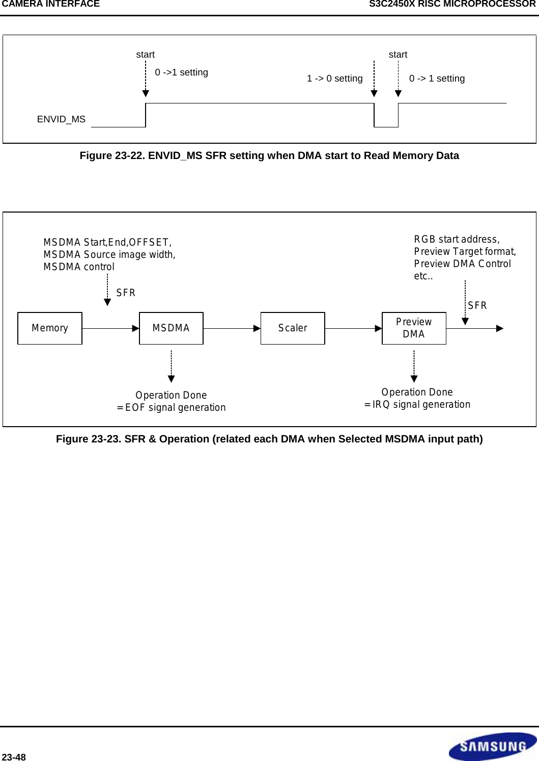
![ADC AND TOUCH SCREEN INTERFACE S3C2450X RISC MICROPROCESSOR 24-2 2 ADC & TOUCH SCREEN INTERFACE OPERATION 2.1 BLOCK DIAGRAM Figure 24-1 shows the functional block diagram of A/D converter and touch screen interface. Note that the A/D converter device is a recycling type. 10:1MUXPULL_UPXM_SENYM_SENXP_SENYP_SENTouch screenpads controlA/DConverterADC interface& Touch screen controlADC input controlInterrupt generationSUBINT_ADCSUBINT_TCWaiting for interruptVDDA_ADCVDDA_ADCAIN9(XP)AIN8(XM)AIN7(YP)AIN6(YM)AIN[5:0]VDDA_ADC Figure 24-1. ADC and Touch Screen Interface Block Diagram](https://usermanual.wiki/Diasonic-Technology-Co/RVM-704M.Users-Manual/User-Guide-1826140-Page-674.png)
![ADC AND TOUCH SCREEN INTERFACE S3C2450X RISC MICROPROCESSOR 24-4 4. Waiting for interrupt mode (ADCTSC = 0xd3) Touch screen controller generates interrupt (INT_TC) signal when the stylus is down. The value of ADC touch screen control register (ADCTSC) is ‘0xd3’; PULL_UP is ‘0’, XP_SEN is ‘1’, XM_SEN is ‘0’, YP_SEN is ‘1’ and YM_SEN is ‘1’. Touch interrupt can be generated when stylus pen is down or up. After touch screen controller generates interrupt signal (INT_TC), waiting for interrupt mode must be cleared. (XY_PST sets to the No operation Mode) Mode XP XM YP YM Waiting for Interrupt Mode VDDA_ADC(Pull-up enable) Hi-z Hi-z VSSA_ADC 2.2.3 Standby Mode Standby mode is activated when ADCCON [2] is set to '1'. In this mode, A/D conversion operation is halted and ADCDAT0, ADCDAT1 register contains the previous converted data. 2.2.4 Programming Notes 1. The A/D converted data can be accessed by means of interrupt or polling method. With interrupt method, the overall conversion time - from A/D converter start to converted data read - may be delayed because of the return time of interrupt service routine and data access time. With polling method, by checking the ADCCON[15] - end of conversion flag-bit, the read time from ADCDAT register can be determined. 2. A/D conversion can be activated in different way: After ADCCON[1] - A/D conversion start-by-read mode-is set to 1, A/D conversion starts simultaneously whenever converted data is read. Stylus DownX-Conversion Y-ConversionStylus UpAB C= x (1/X-tal clock) or x (1/EXTCLK clock)= x (1/PCLK clock) + 5 x (1/PCLK clock) x (PRSCVL+1)= x (1/PCLK clock) + 5 x (1/PCLK clock) x (PRSCVL+1)= Delay value of ADCDLY registerXPYP Figure 24-2. Timing Diagram in Auto (Sequential) X/Y Position Conversion Mode](https://usermanual.wiki/Diasonic-Technology-Co/RVM-704M.Users-Manual/User-Guide-1826140-Page-676.png)
![S3C2450X RISC MICROPROCESSOR ADC AND TOUCH SCREEN INTERFACE 24-5 3 ADC AND TOUCH SCREEN INTERFACE SPECIAL REGISTERS 3.1 ADC CONTROL (ADCCON) REGISTER Register Address R/W Description Reset ValueADCCON 0x58000000 R/W ADC control register 0x3FC4 ADCCON Bit Description Initial StateECFLG [15] End of conversion flag (read only). 0 = A/D conversion in process 1 = End of A/D conversion 0 PRSCEN [14] A/D converter prescaler enable. 0 = Disable 1 = Enable 0 PRSCVL [13:6] A/D converter prescaler value. Data value: 5 ~ 255 Note that division factor is (N+1) when the prescaler value is N. Note: ADC frequency should be set less than PCLK by 5 times. (Ex. PCLK = 10MHz, ADC Frequency < 2MHz) 0xFF Reserved [5:4] Reserved 0 RESSEL [3] A/D converter resolution selection 0 = 10-bit resolution 1 = 12-bit resolution 0 STDBM [2] Standby mode select. 0 = Normal operation mode 1 = Standby mode 1 READ_ START [1] A/D conversion starts by read. 0 = Disable start by read operation 1 = Enable start by read operation 0 ENABLE_ START [0] A/D conversion starts by setting this bit. If READ_START is enabled, this value is not valid. 0 = No operation 1 = A/D conversion starts and this bit is cleared after the start-up. 0](https://usermanual.wiki/Diasonic-Technology-Co/RVM-704M.Users-Manual/User-Guide-1826140-Page-677.png)
![ADC AND TOUCH SCREEN INTERFACE S3C2450X RISC MICROPROCESSOR 24-6 3.2 ADC TOUCH SCREEN CONTROL (ADCTSC) REGISTER Register Address R/W Description Reset ValueADCTSC 0x58000004 R/W ADC touch screen control register 0x058 ADCTSC Bit Description Initial StateUD_SEN [8] Select interrupt source Stylus Up or Down 0 = Detect Stylus Down Signal. 1 = Detect Stylus Up Signal. 0 YM_SEN [7] YM to GND Switch Enable 0 = Switch disable.(YM = AIN6, Hi-z) 1 = Switch enable.(YM = VSSA_ADC) 0 YP_SEN [6] YP to VDD Switch Enable 0 = Switch enable.(YP = VDDA_ADC) 1 = Switch disable.(YP = AIN7, Hi-z) 1 XM_SEN [5] XM to GND Switch Enable 0 = Switch disable.(XM = AIN8, Hi-z) 1 = Switch enable.(XM = VSSA_ADC) 0 XP_SEN [4] XP to VDD Switch Enable 0 = Switch enable.(XP = VDDA_ADC) 1 = Switch disable.(XP = AIN9, Hi-z) 1 PULL_UP [3] XP Pull-up Switch Enable 0 = XP pull-up enable. 1 = XP pull-up disable. 1 AUTO_PST [2] Automatically sequencing conversion of X-Position and Y-Position 0 = Normal ADC conversion. 1 = Auto measurement of X-position, Y-position. 0 XY_PST [1:0] Manually measurement of X-Position or Y-Position. 00 = No operation mode 01 = X-position measurement 10 = Y-position measurement 11 = Waiting for Interrupt Mode 0 NOTES: 1. While waiting for Touch screen Interrupt, XP_SEN bit should be set to ‘1’(XP Output disable) and PULL_UP bit should be set to ‘0’(XP Pull-up enable). 2. AUTO_PST bit should be set ‘1’ only in Automatic (Sequential) X/Y Position conversion. 3. PULL_UP switche should be eabled during stop/sleep mode to avoid leakage current.](https://usermanual.wiki/Diasonic-Technology-Co/RVM-704M.Users-Manual/User-Guide-1826140-Page-678.png)
![S3C2450X RISC MICROPROCESSOR ADC AND TOUCH SCREEN INTERFACE 24-7 3.3 ADC START DELAY (ADCDLY) REGISTER Register Address R/W Description Reset ValueADCDLY 0x58000008 R/W ADC start or interval delay register 0x00ff ADCDLY Bit Description Initial StateDELAY [15:0] Incase of ADC conversion mode (Normal, Separate, Auto conversion); ADC conversion is delayed by counting this value. Counting clock is PCLK. In case of waiting for interrupt mode; When stylus down occurs in waiting for interrupt mode, counts this value and then generates Interrupt signal (INT_TC) for filtering noise. Counting clock is external input clock (X-tal or EXTCLK). Note: Do not use zero value (0x0000) 0x00ff](https://usermanual.wiki/Diasonic-Technology-Co/RVM-704M.Users-Manual/User-Guide-1826140-Page-679.png)
![ADC AND TOUCH SCREEN INTERFACE S3C2450X RISC MICROPROCESSOR 24-8 3.4 ADC CONVERSION DATA (ADCDAT0) REGISTER Register Address R/W Description Reset ValueADCDAT0 0x5800000C R ADC conversion data register - ADCDAT0 Bit Description Initial StateUPDOWN [15] Up or down state of Stylus at Waiting for Interrupt Mode. 0 = Stylus down state 1 = Stylus up state - AUTO_PST [14] Automatic sequencing conversion of X-position and Y-position. (mirroring AUTO_PST in ADCTSC register) 0 = Normal ADC conversion 1 = Auto measurement of X-position, Y-position - XY_PST [13:12] Manual measurement of X-position or Y-position. (mirroring XY_PST in ADCTSC register) 00 = No operation mode 01 = X-position measurement 10 = Y-position measurement 11 = Waiting for Interrupt Mode - XPDATA_12 (Normal ADC) [11:10] When A/D resolution is 12bit, X-position conversion MSB 2-bit data value (include Normal ADC conversion data) Data value(data [11:0]) = 0 ~ 0xFFF - XPDATA (Normal ADC) [9:0] X-position conversion data value. (include Normal ADC conversion data value) Data value(data [9:0]) = 0 ~ 0x3FF -](https://usermanual.wiki/Diasonic-Technology-Co/RVM-704M.Users-Manual/User-Guide-1826140-Page-680.png)
![S3C2450X RISC MICROPROCESSOR ADC AND TOUCH SCREEN INTERFACE 24-9 3.5 ADC CONVERSION DATA (ADCDAT1) REGISTER Register Address R/W Description Reset ValueADCDAT1 0x58000010 R ADC conversion data register - ADCDAT1 Bit Description Initial StateUPDOWN [15] Up or down state of Stylus at Waiting for Interrupt Mode. 0 = Stylus down state 1 = Stylus up state - AUTO_PST [14] Automatic sequencing conversion of X-position and Y-position. (mirroring AUTO_PST in ADCTSC register) 0 = Normal ADC conversion 1 = Auto measurement of X-position, Y-position - XY_PST [13:12] Manual measurement of X-position or Y-position. (mirroring XY_PST in ADCTSC register) 00 = No operation mode 01 = X-position measurement 10 = Y-position measurement 11 = Waiting for Interrupt Mode - YPDATA_12 [11:10] When A/D resolution is 12bit, X-position conversion MSB 2-bit data value. Data value(data [11:0]) = 0 ~ 0xFFF YPDATA [9:0] Y-position conversion data value. Data value(data [9:0]) = 0 ~ 0x3FF - 3.6 ADC TOUCH SCREEN UP-DOWN INT CHECK REGISTER (ADCUPDN) Register Address R/W Description Reset ValueADCUPDN 0x5800014 R/W Stylus Up or Down Interrpt state register 0x0 ADCUPDN Bit Description Initial StateTSC_UP [1] Stylus Up Interrupt history. (After check, this bit should be cleared manually) 0 = No stylus up state. 1 = Stylus up interrupt has been occurred. 0 TSC_DN [0] Stylus Down Interrupt history. (After check, this bit should be cleared manually) 0 = No stylus down state. 1 = Stylus down interrupt has been occurred. 0](https://usermanual.wiki/Diasonic-Technology-Co/RVM-704M.Users-Manual/User-Guide-1826140-Page-681.png)
![ADC AND TOUCH SCREEN INTERFACE S3C2450X RISC MICROPROCESSOR 24-10 3.7 ADC CHANNEL MUX REGISTER (ADCMUX) Register Address R/W Description Reset ValueADCMUX 0x5800018 R/W Analog input channel select 0x0 ADCMUX Bit Description Initial StateADCMUX [3:0] Analog input channel select. 0000 = AIN 0 0001 = AIN 1 0010 = AIN 2 0011 = AIN 3 0100 = AIN 4 0101 = AIN 5 0110 = AIN 6 (YM) 0111 = AIN 7 (YP) 1000 = AIN8 (XM) 1001 = AIN9 (XP) 0 NOTE: When Touch Screen Pads(YM, YP, XM, XP) are disabled, these ports can be used as Analog input ports(AIN6, AIN7, AIN8, AIN9) for ADC.](https://usermanual.wiki/Diasonic-Technology-Co/RVM-704M.Users-Manual/User-Guide-1826140-Page-682.png)
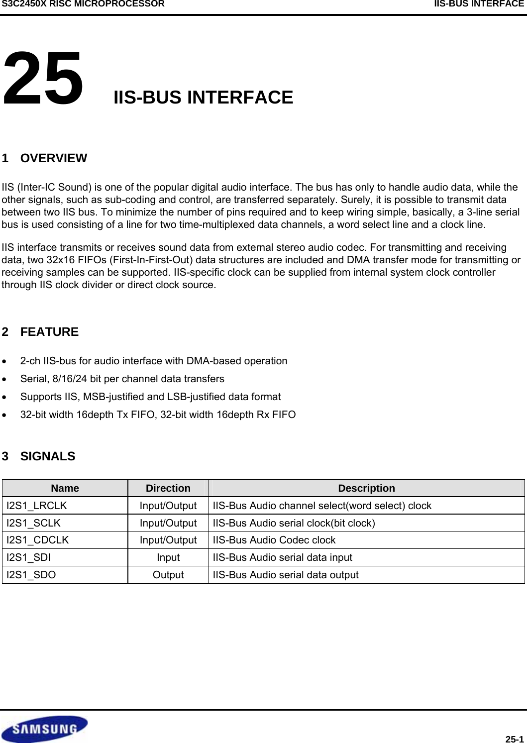
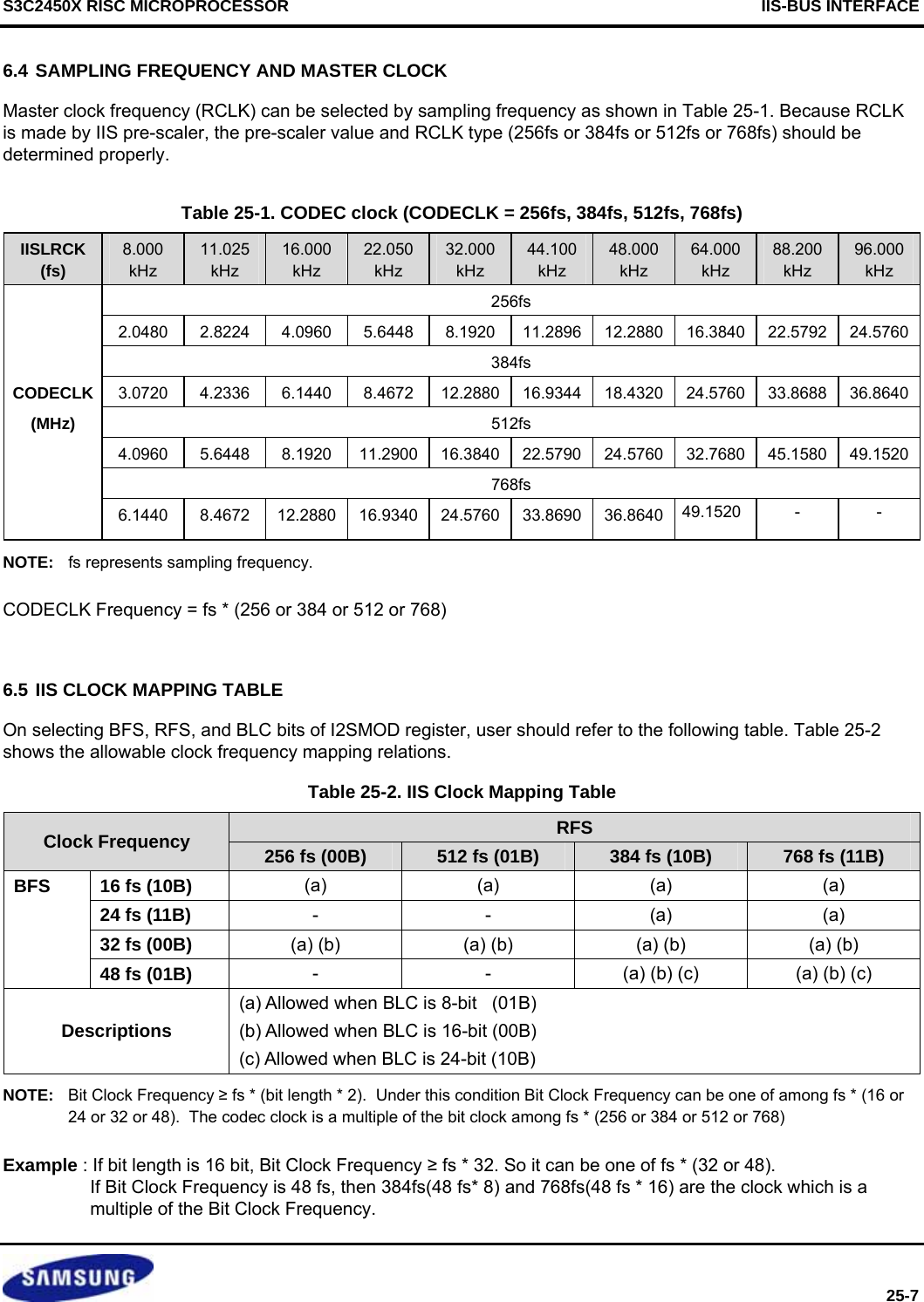
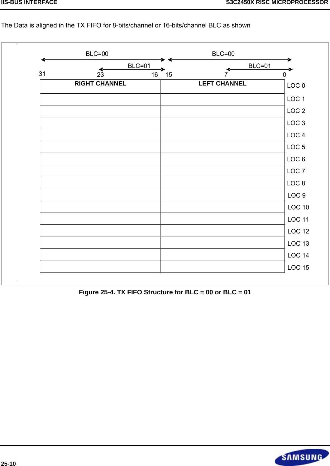
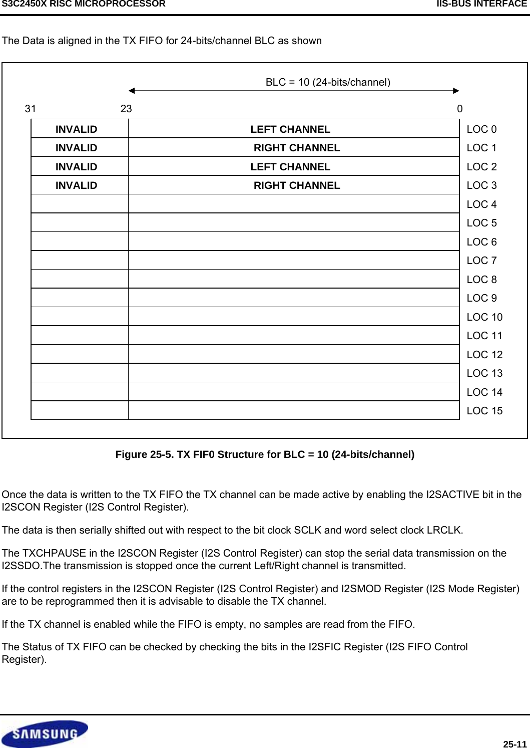
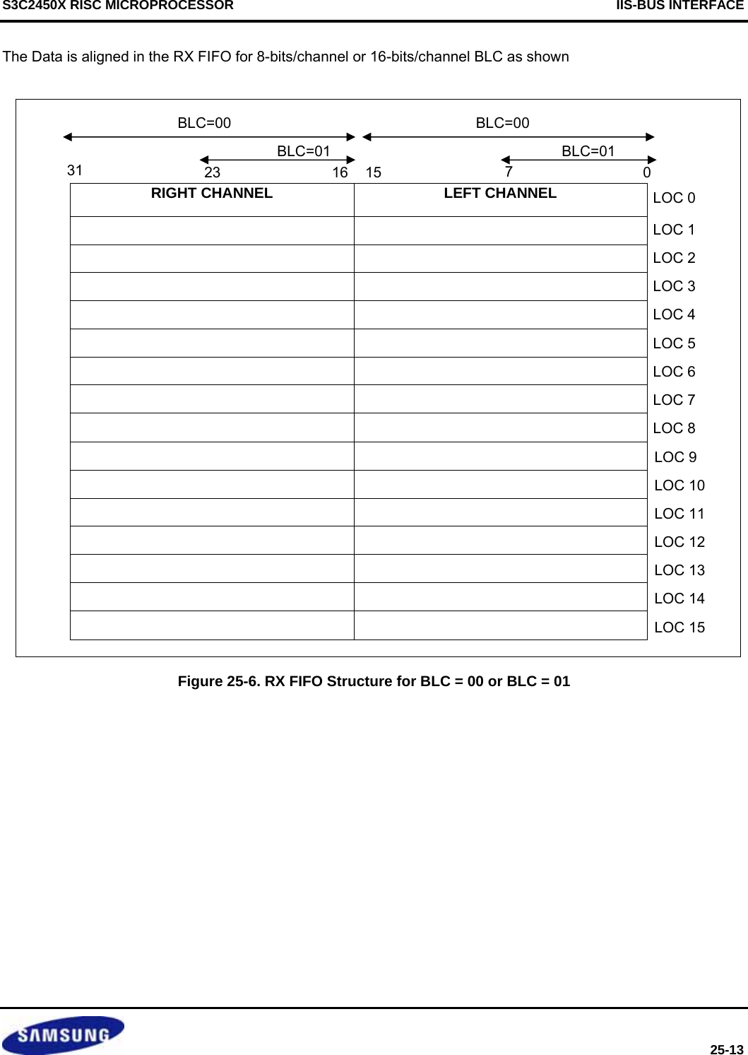
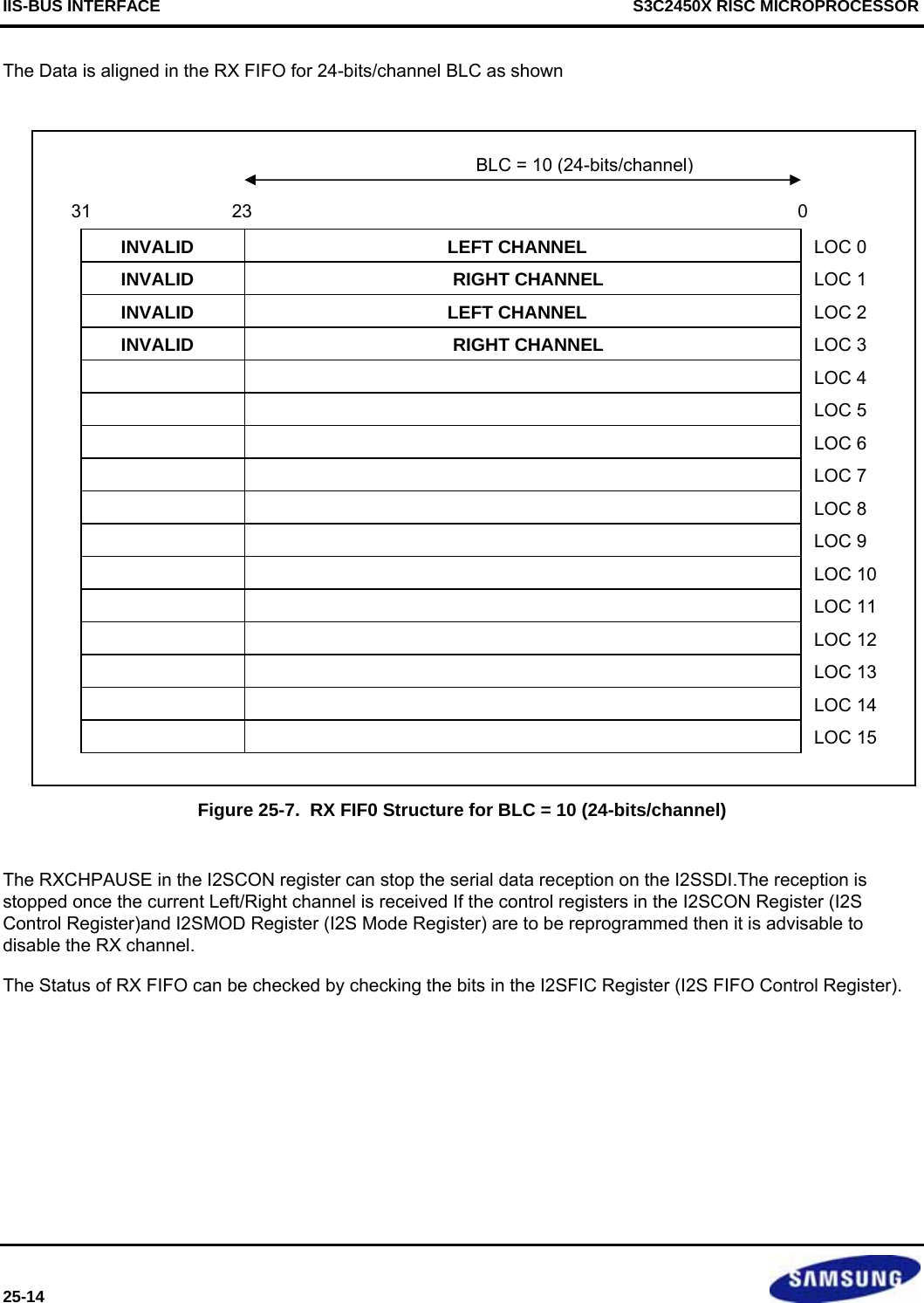
![IIS-BUS INTERFACE S3C2450X RISC MICROPROCESSOR 25-16 8.1 IIS CONTROL REGISTER (IISCON) Register Address Description Reset Value IISCON 0x55000100 IIS interface control register 0x0000_0600 IISCON Bit R/W Description [31:18] R/W Reserved. Program to zero. FTXURSTATUS [17] R/W TX FIFO under-run interrupt status. And this is used by interrupt clear bit. When this is high, you can do interrupt clear by writing ‘1’. 0 = Interrupt didn’t be occurred. 1 = Interrupt was occurred. FTXURINTEN [16] R/W TX FIFO Under-run Interrupt Enable 0 = TXFIFO Under-run INT disable 1 = TXFIFO Under-run INT enable1) [15:12] R/W Reserved. Program to zero. LRI [11] R Left/Right channel clock indication. Note that LRI meaning is dependent on the value of LRP bit of I2SMOD register. 0 = Left (when LRP bit is low) or right (when LRP bit is high) 1 = Right (when LRP bit is low) or left (when LRP bit is high) FTXEMPT [10] R Tx FIFO empty status indication. 0 = FIFO is not empty (ready for transmit data to channel) 1 = FIFO is empty (not ready for transmit data to channel) FRXEMPT [9] R Rx FIFO empty status indication. 0 = FIFO is not empty 1 = FIFO is empty FTXFULL [8] R Tx FIFO full status indication. 0 = FIFO is not full 1 = FIFO is full FRXFULL [7] R Rx FIFO full status indication. 0 = FIFO is not full (ready for receive data from channel) 1 = FIFO is full (not ready for receive data from channel) TXDMAPAUSE [6] R/W Tx DMA operation pause command. Note that when this bit is activated at any time, the DMA request will be halted after current on-going DMA transfer is completed. 0 = No pause DMA operation 1 = Pause DMA operation](https://usermanual.wiki/Diasonic-Technology-Co/RVM-704M.Users-Manual/User-Guide-1826140-Page-698.png)
![S3C2450X RISC MICROPROCESSOR IIS-BUS INTERFACE 25-17 IISCON Bit R/W Description RXDMAPAUSE [5] R/W Rx DMA operation pause command. Note that when this bit is activated at any time, the DMA request will be halted after current on-going DMA transfer is completed. 0 = No pause DMA operation 1 = Pause DMA operation TXCHPAUSE [4] R/W Tx channel operation pause command. Note that when this bit is activated at any time, the channel operation will be halted after left-right channel data transfer is completed. 0 = No pause operation 1 = Pause operation RXCHPAUSE [3] R/W Rx channel operation pause command. Note that when this bit is activated at any time, the channel operation will be halted after left-right channel data transfer is completed. 0 = No pause operation 1 = Pause operation TXDMACTIVE [2] R/W Tx DMA active (start DMA request). Note that when this bit is set from high to low, the DMA operation will be forced to stop immediately. 0 = Inactive 1 = Active RXDMACTIVE [1] R/W Rx DMA active (start DMA request). Note that when this bit is set from high to low, the DMA operation will be forced to stop immediately. 0 = Inactive 1 = Active I2SACTIVE [0] R/W IIS interface active (start operation). 0 = Inactive 1 = Active NOTE: When playing is finished, Under-run interrupt will be occurring. (Since no more data are written into TXFIFO at the end of playing.) User can stop transmission at this Under-run interrupt.](https://usermanual.wiki/Diasonic-Technology-Co/RVM-704M.Users-Manual/User-Guide-1826140-Page-699.png)
![IIS-BUS INTERFACE S3C2450X RISC MICROPROCESSOR 25-18 8.2 IIS MODE REGISTER (IISMOD) Register Address Description Reset Value IISMOD 0x55000104 IIS interface mode register 0x0000_0000 IISMOD Bit R/W Description [31:15] R/W Reserved. Program to zero. BLC [14:13] R/W Bit Length Control Bit Which decides transmission of 8/16 bits per audio channel 00 =16 Bits per channel 01 = 8 Bits Per Channel 10 = 24 Bits Per Channel 11 = Reserved CDCLKCON [12] R/W Determine direction of codec clock(I2SCDCLK) 0 = Supply codec clock to external codec chip. (from PCLK, EPLL, EPLLRefCLK) 1 = Get codec clock from external codec chip. (to CLKAUDIO) (Refer to Figure 25-2) IMS [11:10] R/W IIS master or slave mode select. (and select source of codec clock) 00 = Master mode (PCLK is source clock for I2SSCLK, I2SLRCLK, I2SCDCLK) 01 = Master mode (CLKAUDIO is source clock for I2SSCLK, I2SLRCLK. CLKAUDIO-EPLL, EPLLRefCLK is source clock for I2SCDCLK) 10 = Slave mode (PCLK is source clock for I2SCDCLK) 11 = Slave mode (CLKAUDIO-EPLL, EPLLRefCLK is source clock for I2SCDCLK) (Refer to Figure 25-2) TXR [9:8] R/W Transmit or receive mode select. 00 = Transmit only mode 01 = Receive only mode 10 = Transmit and receive simultaneous mode 11 = Reserved LRP [7] R/W Left/Right channel clock polarity select. 0 = Low for left channel and high for right channel 1 = High for left channel and low for right channel SDF [6:5] R/W Serial data format. 00 = IIS format 01 = MSB-justified (left-justified) format 10 = LSB-justified (right-justified) format 11 = Reserved](https://usermanual.wiki/Diasonic-Technology-Co/RVM-704M.Users-Manual/User-Guide-1826140-Page-700.png)
![S3C2450X RISC MICROPROCESSOR IIS-BUS INTERFACE 25-19 IISMOD Bit R/W Description RFS [4:3] R/W IIS root clock (codec clock) frequency select. 00 = 256 fs, where fs is sampling frequency 01 = 512 fs 10 = 384 fs 11 = 768 fs (Even in the slave mode, this bit should be set for correct) BFS [2:1] R/W Bit clock frequency select. 00 = 32 fs, where fs is sampling frequency 01 = 48 fs 10 = 16 fs 11 = 24 fs (Even in the slave mode, this bit should be set for correct) [0] R/W Reserved. Program to zero.](https://usermanual.wiki/Diasonic-Technology-Co/RVM-704M.Users-Manual/User-Guide-1826140-Page-701.png)
![IIS-BUS INTERFACE S3C2450X RISC MICROPROCESSOR 25-20 8.3 IIS FIFO CONTROL REGISTER (IISFIC) Register Address Description Reset Value IISFIC 0x55000108 IIS interface FIFO control register 0x0000_0000 IISFIC Bit R/W Description [31:16] R/W Reserved. Program to zero. TFLUSH [15] R/W TX FIFO flush command. 0 = No flush 1 = Flush [14:13] R/W Reserved. Program to zero. FTXCNT [12:8] R TX FIFO data count. (0~16) RFLUSH [7] R/W RX FIFO flush command. 0 = No flush 1 = Flush [6:5] R/W Reserved. Program to zero. FRXCNT [4:0] R RX FIFO data count. (0~16) NOTE: Tx FIFOs, Rx FIFO has 32-bit width and 16 depth structure, so FIFO data count value ranges from 0 to 16. 8.4 IIS PRESCALER CONTROL REGISTER (IISPSR) Register Address Description Reset Value IISPSR 0x5500010C IIS interface clock divider control register 0x0000_0000 IISPSR Bit R/W Description [31:16] R/W Reserved. Program to zero. PSRAEN [15] R/W Pre-scaler (Clock divider) active. 1 = Active (divide I2SAudioCLK with Pre-scaler division value) 0 = Inactive (bypass I2SAudioCLK) (Refer to Figure 25-2) [14] R/W Reserved. Program to zero. PSVALA [13:8] R/W Pre-scaler (Clock divider) division value. N = Division factor is N+1 (1~1/64) [7:0] R/W Reserved. Program to zero.](https://usermanual.wiki/Diasonic-Technology-Co/RVM-704M.Users-Manual/User-Guide-1826140-Page-702.png)
![S3C2450X RISC MICROPROCESSOR IIS-BUS INTERFACE 25-21 8.5 IIS TRANSMIT REGISTER (IISTXD) Register Address Description Reset Value IISTXD 0x55000110 IIS interface transmit data register 0x0000_0000 IISTXD Bit R/W Description IISTXD [31:0] W TX FIFO write data. Note that the left/right channel data is allocated as the following bit fields. R[23:0], L[23:0] when 24-bit BLC R[31:16], L[15:0] when 16-bit BLC R[23:16], L[7:0] when 8-bit BLC 8.6 IIS RECEIVE REGISTER (IISRXD) Register Address Description Reset Value IISRXD 0x55000114 IIS interface receive data register 0x0000_0000 IISRXD Bit R/W Description IISRXD [31:0] R RX FIFO read data. Note that the left/right channel data is allocated as the following bit fields. R[23:0], L[23:0] when 24-bit BLC R[31:16], L[15:0] when 16-bit BLC R[23:16], L[7:0] when 8-bit BLC](https://usermanual.wiki/Diasonic-Technology-Co/RVM-704M.Users-Manual/User-Guide-1826140-Page-703.png)

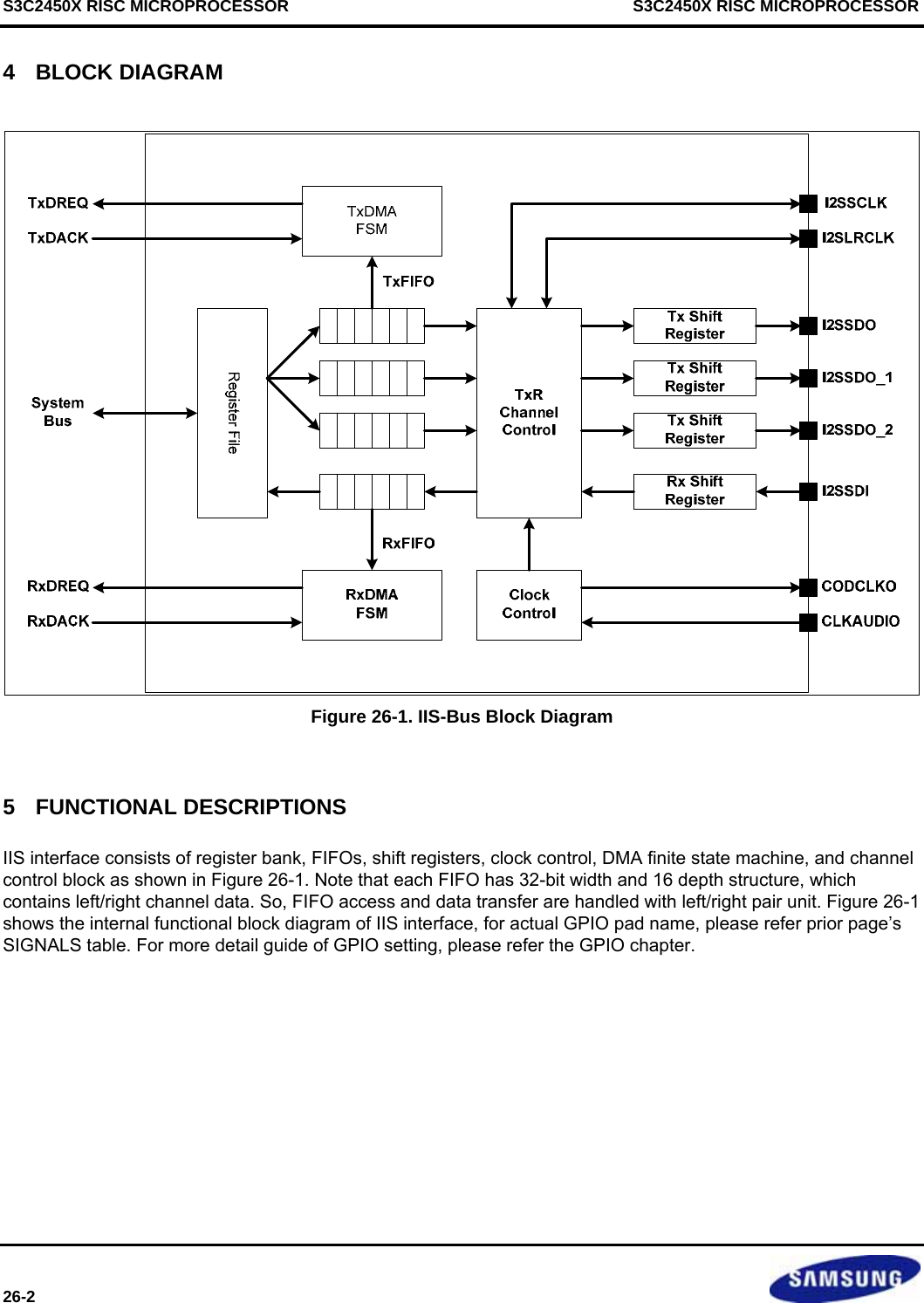
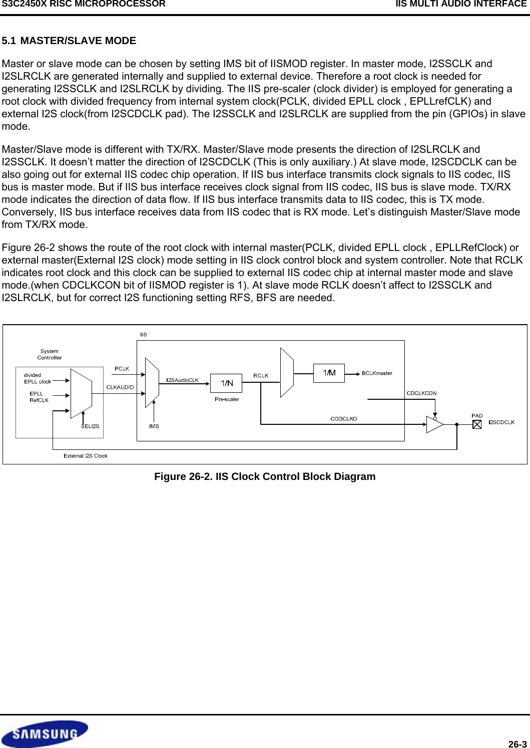
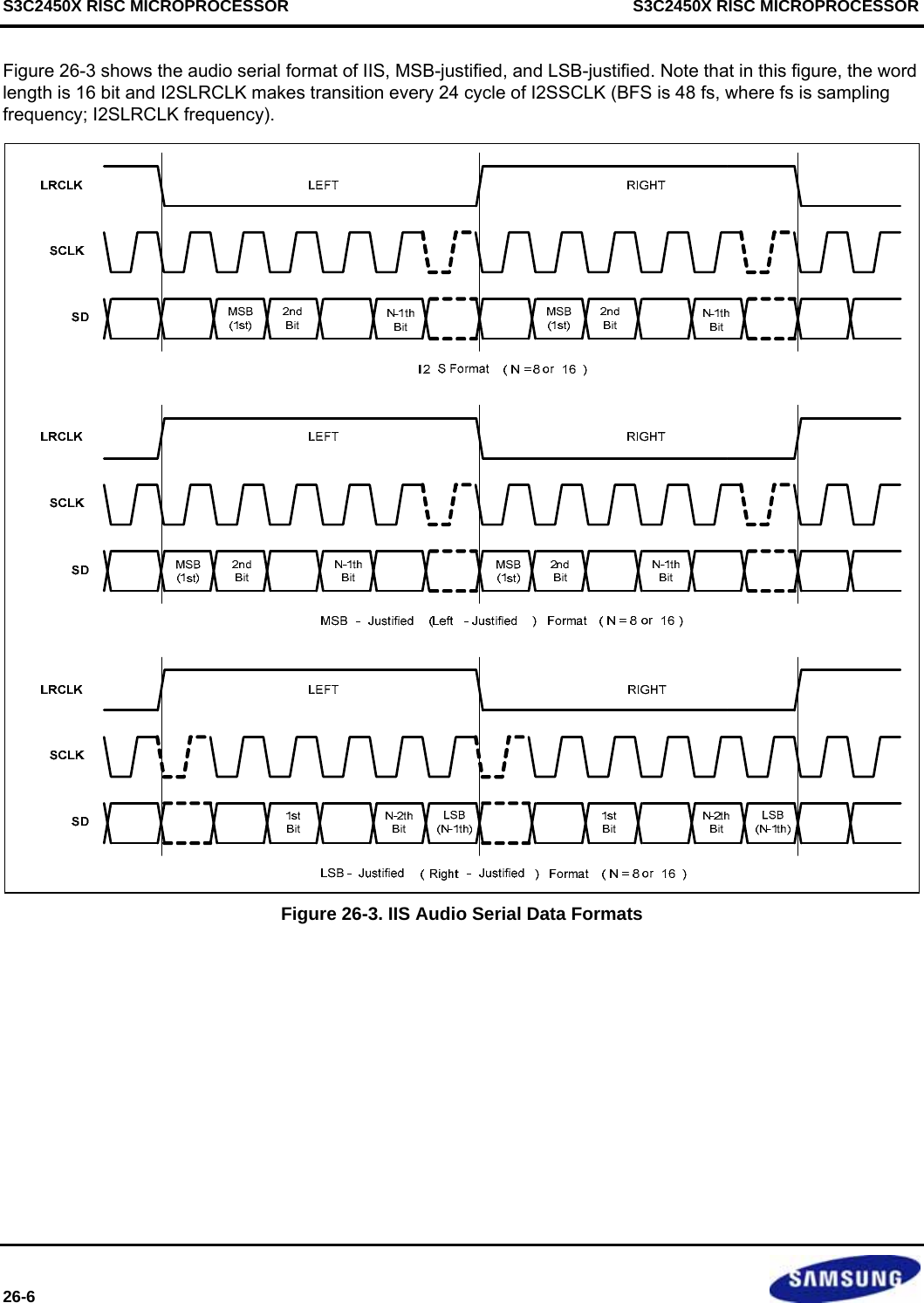
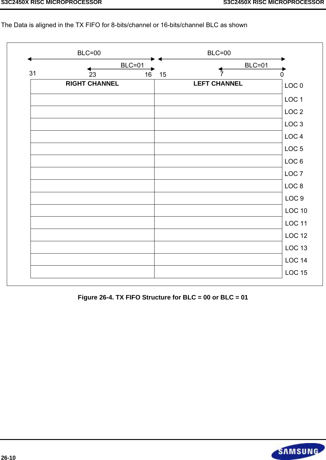
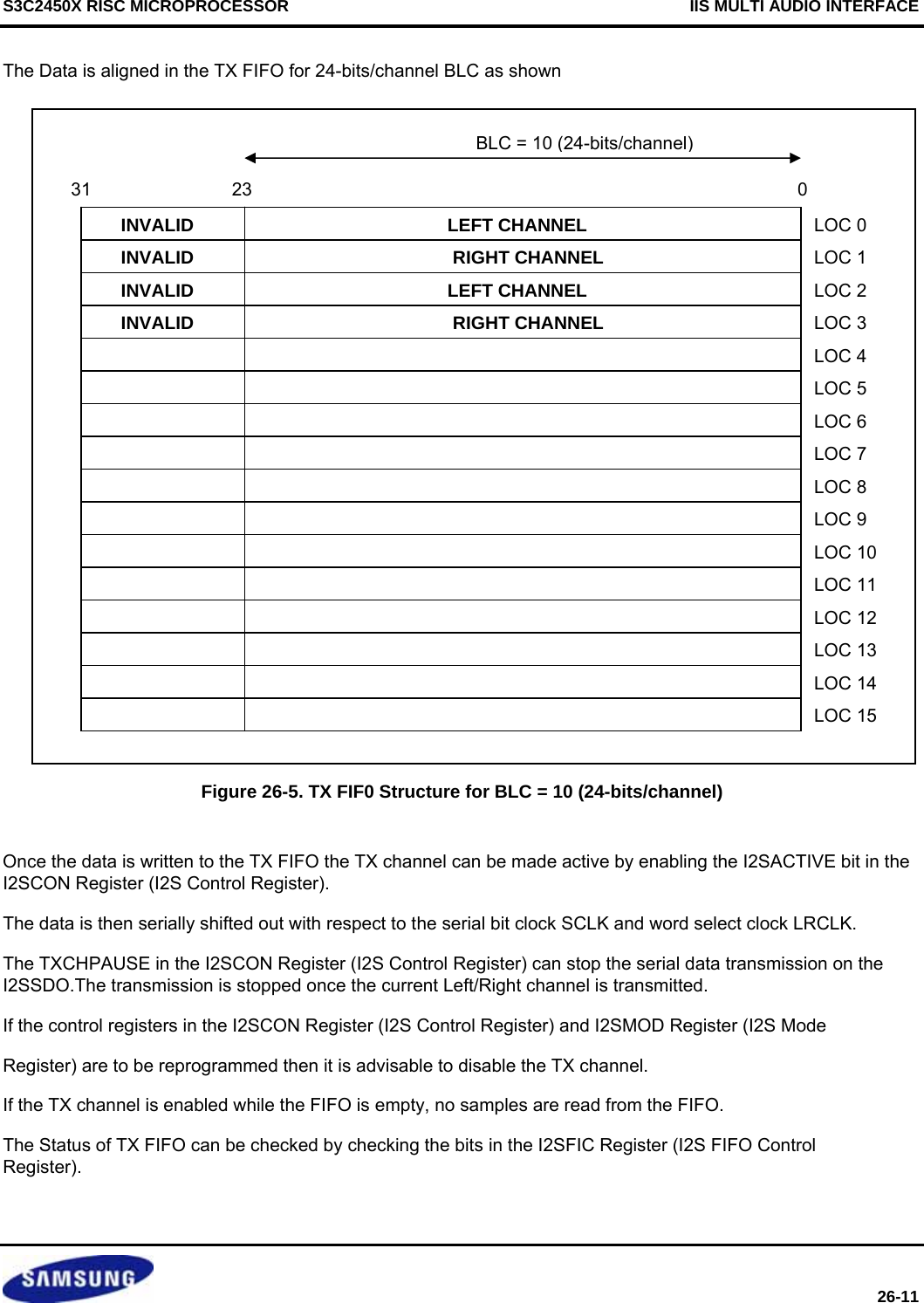


![S3C2450X RISC MICROPROCESSOR S3C2450X RISC MICROPROCESSOR 26-16 8.1 IIS CONTROL REGISTER (IISCON) Register Address Description Reset Value IISCON 0x55000000 IIS interface control register 0x0000_C600 IISCON Bit R/W Description Reserved [31:18] R/W Reserved. Program to zero. FTXURSTATUS [17] R/W TX FIFO under-run interrupt status. And this is used by interrupt clear bit. When this is high, you can do interrupt clear by writing ‘1’. 0 = Interrupt didn’t be occurred. 1 = Interrupt was occurred. FTXURINTEN [16] R/W TX FIFO Under-run Interrupt Enable 0 = TXFIFO Under-run INT disable 1 = TXFIFO Under-run INT enable 1) FTX2EMPT [15] R TX FIFO2 empty Status Indication 0 = TX FIFO2 is not empty(Ready to transmit Data) 1 = TX FIFO2 is empty (Not Ready to transmit Data) FTX1EMPT [14] R TX FIFO1 empty Status Indication 0 = TX FIFO1 is not empty(Ready to transmit Data) 1 = TX FIFO1 is empty (Not Ready to transmit Data) FTX2FULL [13] R TX FIFO2 full Status Indication 0 = TX FIFO2 is not full 1 = TX FIFO2 is full FTX1FULL [12] R TX FIFO1 full Status Indication 0 = TX FIFO1 is not full 1 = TX FIFO1 is full LRI [11] R Left/Right channel clock indication. Note that LRI meaning is dependent on the value of LRP bit of I2SMOD register. 0 = Left (when LRP bit is low) or right (when LRP bit is high) 1 = Right (when LRP bit is low) or left (when LRP bit is high) FTX0EMPT [10] R Tx FIFO0 empty status indication. 0 = FIFO is not empty (ready for transmit data to channel) 1 = FIFO is empty (not ready for transmit data to channel) FRXEMPT [9] R Rx FIFO empty status indication. 0 = FIFO is not empty 1 = FIFO is empty FTX0FULL [8] R Tx FIFO0 full status indication. 0 = FIFO is not full 1 = FIFO is full](https://usermanual.wiki/Diasonic-Technology-Co/RVM-704M.Users-Manual/User-Guide-1826140-Page-720.png)
![S3C2450X RISC MICROPROCESSOR IIS MULTI AUDIO INTERFACE 26-17 IISCON Bit R/W Description FRXFULL [7] R Rx FIFO full status indication. 0 = FIFO is not full (ready for receive data from channel) 1 = FIFO is full (not ready for receive data from channel) TXDMAPAUSE [6] R/W Tx DMA operation pause command. Note that when this bit is activated at any time, the DMA request will be halted after current on-going DMA transfer is completed. 0 = No pause DMA operation 1 = Pause DMA operation RXDMAPAUSE [5] R/W Rx DMA operation pause command. Note that when this bit is activated at any time, the DMA request will be halted after current on-going DMA transfer is completed. 0 = No pause DMA operation 1 = Pause DMA operation TXCHPAUSE [4] R/W Tx channel operation pause command. Note that when this bit is activated at any time, the channel operation will be halted after left-right channel data transfer is completed. 0 = No pause operation 1 = Pause operation RXCHPAUSE [3] R/W Rx channel operation pause command. Note that when this bit is activated at any time, the channel operation will be halted after left-right channel data transfer is completed. 0 = No pause operation 1 = Pause operation TXDMACTIVE [2] R/W Tx DMA active (start DMA request). Note that when this bit is set from high to low, the DMA operation will be forced to stop immediately. 0 = Inactive 1 = Active RXDMACTIVE [1] R/W Rx DMA active (start DMA request). Note that when this bit is set from high to low, the DMA operation will be forced to stop immediately. 0 = Inactive 1 = Active I2SACTIVE [0] R/W IIS interface active (start operation). 0 = Inactive 1 = Active NOTE: When playing is finished, Under-run interrupt will be occurring. (Since no more data are written into TXFIFO at the end of playing.) User can stop transmission at this Under-run interrupt.](https://usermanual.wiki/Diasonic-Technology-Co/RVM-704M.Users-Manual/User-Guide-1826140-Page-721.png)
![S3C2450X RISC MICROPROCESSOR S3C2450X RISC MICROPROCESSOR 26-18 8.2 IIS MODE REGISTER (IISMOD) Register Address Description Reset Value IISMOD 0x55000004 IIS interface mode register 0x0000_0000 IISMOD Bit R/W Description Reserved [31:15] R/W Reserved. Program to zero. CDD2 [21:20] R/W Channel-2 Data Discard. Discard means zero padding. It only supports 8/16 bit mode. 00 = No Discard 01 = I2STXD[15:0] Discard 10 = I2STXD[31:16] Discard 11 = Reserved CDD1 [19:18] R/W Channel-1 Data Discard. Discard means zero padding. It only supports 8/16 bit mode. 00 = No Discard 01 = I2STXD[15:0] Discard 10 = I2STXD[31:16] Discard 11 = Reserved DCE [17:16] R/W Data Channel Enable. [17] = SD2 channel enable [16] = SD1 channel enable [15] R/W Reserved, Program to Zero BLC [14:13] R/W Bit Length Control Bit Which decides transmission of 8/16 bits per audio channel 00 = 16 Bits per channel 01 = 8 Bits Per Channel 10 = 24 Bits Per Channel 11 = Reserved CDCLKCON [12] R/W Determine direction of codec clock(I2SCDCLK) 0 = Supply codec clock to external codec chip. (from PCLK, EPLL, EPLLRefCLK) 1 = Get codec clock from external codec chip. (to CLKAUDIO) (Refer to Figure 26-2) IMS [11:10] R/W IIS master or slave mode select. (and select source of codec clock) 00 = Master mode (PCLK is source clock for I2SSCLK, I2SLRCLK, I2SCDCLK) 01 = Master mode (CLKAUDIO is source clock for I2SSCLK, I2SLRCLK. CLKAUDIO-EPLL, EPLLRefCLK is source clock for I2SCDCLK) 10 = Slave mode (PCLK is source clock for I2SCDCLK) 11 = Slave mode (CLKAUDIO-EPLL, EPLLRefCLK is source clock for I2SCDCLK) (Refer to Figure 26-2)](https://usermanual.wiki/Diasonic-Technology-Co/RVM-704M.Users-Manual/User-Guide-1826140-Page-722.png)
![S3C2450X RISC MICROPROCESSOR IIS MULTI AUDIO INTERFACE 26-19 IISMOD Bit R/W Description TXR [9:8] R/W Transmit or receive mode select. 00 = Transmit only mode 01 = Receive only mode 10 = Transmit and receive simultaneous mode 11 = Reserved LRP [7] R/W Left/Right channel clock polarity select. 0 = Low for left channel and high for right channel 1 = High for left channel and low for right channel SDF [6:5] R/W Serial data format. 00 = IIS format 01 = MSB-justified (left-justified) format 10 = LSB-justified (right-justified) format 11 = Reserved RFS [4:3] R/W IIS root clock (codec clock) frequency select. 00 = 256 fs, where fs is sampling frequency 01 = 512 fs 10 = 384 fs 11 = 768 fs (Even in the slave mode, this bit should be set for correct) BFS [2:1] R/W Bit clock frequency select. 00 = 32 fs, where fs is sampling frequency 01 = 48 fs 10 = 16 fs 11 = 24 fs (Even in the slave mode, this bit should be set for correct) [0] R/W Reserved. Program to zero.](https://usermanual.wiki/Diasonic-Technology-Co/RVM-704M.Users-Manual/User-Guide-1826140-Page-723.png)
![S3C2450X RISC MICROPROCESSOR S3C2450X RISC MICROPROCESSOR 26-20 8.3 IIS FIFO CONTROL REGISTER (IISFIC) Register Address Description Reset Value IISFIC 0x55000008 IIS interface FIFO control register 0x0000_0000 IISFIC Bit R/W Description [31:29] R/W Reserved. Program to zero. FTX2CNT [28:24] R TX FIFO2 data count. (0 ~ 16) [23:21] R/W Reserved. Program to zero. FTX1CNT [20:16] R TX FIFO1 data count. (0~16) TFLUSH [15] R/W TX FIFO flush command. 0 = No flush 1 = Flush [14:13] R/W Reserved. Program to zero. FTX0CNT [12:8] R TX FIFO0 data count. (0~16) RFLUSH [7] R/W RX FIFO flush command. 0 = No flush 1 = Flush [6:5] R/W Reserved. Program to zero. FRXCNT [4:0] R RX FIFO data count. (0~16) NOTE: Tx FIFOs, Rx FIFO has 32-bit width and 16 depth structure, so FIFO data count value ranges from 0 to 16. 8.4 IIS PRESCALER CONTROL REGISTER (IISPSR) Register Address Description Reset Value IISPSR 0x5500000C IIS interface clock divider control register 0x0000_0000 IISPSR Bit R/W Description [31:16] R/W Reserved. Program to zero. PSRAEN [15] R/W Pre-scaler (Clock divider) active. 1 = Active (divide I2SAudioCLK with Pre-scaler division value) 0 = Inactive (bypass I2SAudioCLK) (Refer to Figure 26-2) [14] R/W Reserved. Program to zero. PSVALA [13:8] R/W Pre-scaler (Clock divider) division value. N: Division factor is N+1 (1~1/64) [7:0] R/W Reserved. Program to zero.](https://usermanual.wiki/Diasonic-Technology-Co/RVM-704M.Users-Manual/User-Guide-1826140-Page-724.png)
![S3C2450X RISC MICROPROCESSOR IIS MULTI AUDIO INTERFACE 26-21 8.5 IIS TRANSMIT REGISTER (IISTXD) Register Address Description Reset Value IISTXD 0x55000010 IIS interface transmit data register 0x0000_0000 IISTXD Bit R/W Description IISTXD [31:0] W TX FIFO write data. Note that the left/right channel data is allocated as the following bit fields. R[23:0], L[23:0] when 24-bit BLC R[31:16], L[15:0] when 16-bit BLC R[23:16], L[7:0] when 8-bit BLC 8.6 IIS RECEIVE REGISTER (IISRXD) Register Address Description Reset Value IISRXD 0x55000014 IIS interface receive data register 0x0000_0000 IISRXD Bit R/W Description IISRXD [31:0] R RX FIFO read data. Note that the left/right channel data is allocated as the following bit fields. R[23:0], L[23:0] when 24-bit BLC R[31:16], L[15:0] when 16-bit BLC R[23:16], L[7:0] when 8-bit BLC](https://usermanual.wiki/Diasonic-Technology-Co/RVM-704M.Users-Manual/User-Guide-1826140-Page-725.png)

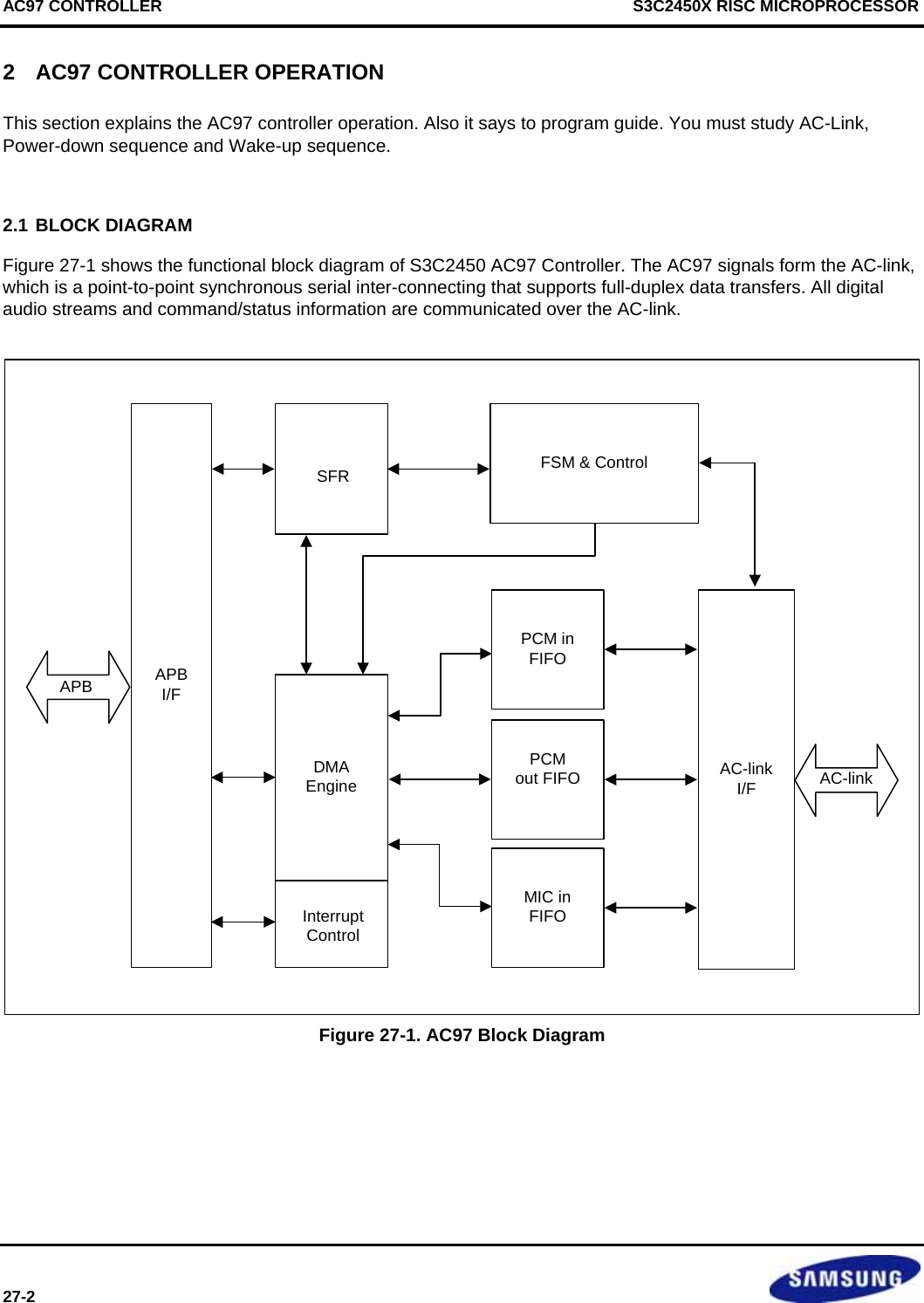
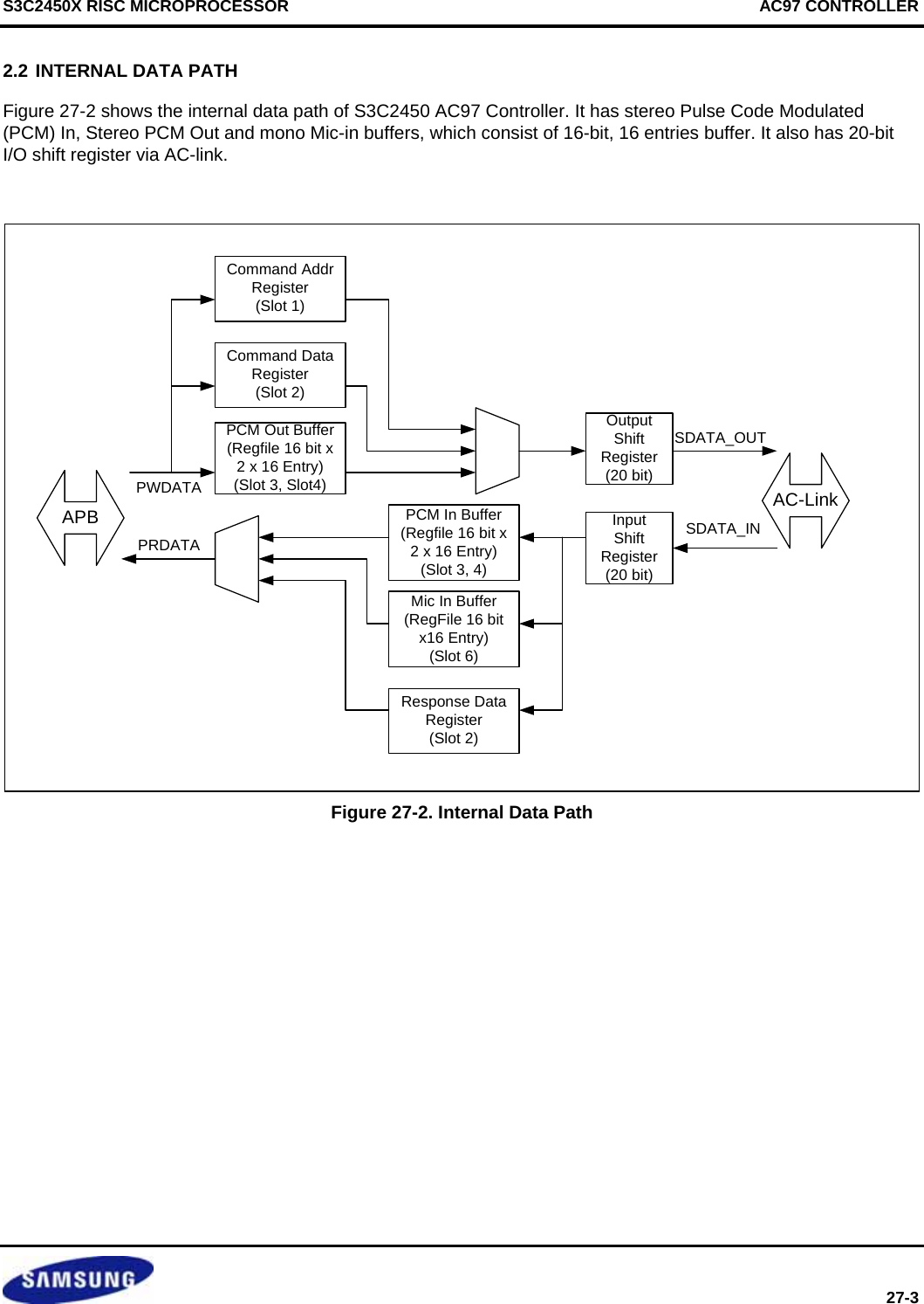
![AC97 CONTROLLER S3C2450X RISC MICROPROCESSOR 27-6 4.1 AC-LINK OUTPUT FRAME (SDATA_OUT) Slot 0: Tag Phase In slot 0, the first bit is a bit (SDATA_OUT, bit 15) which represents the validity of the entire frame. If bit 15 is a 1, the current frame contains at least a valid time slot. The next 12 bit positions correspond each 12 time slot contains valid data. Bits 0 and 1 of slot 0 are used as CODEC IO bits for I/O reads and writes to the CODEC registers as described in the next section. In this way, data streams of differing sample rate can be transmitted across AC-link at its fixed 48kHz audio frame rate. Slot 1: Command Address Port In slot 1, it communicates control register address and write/read command information to the AC97 controller. When software accesses the primary CODEC, the hardware configures the frame as follows : • In slot 0, the valid bit for 1, 2 slots are set. • In slot 1, bit 19 is set (read) or clear(write). Bits 18-12 (of slot 1) are configured to specify the index to the CODEC register. Others are filled with 0’s(reserved). • In slot 2, it configured with the data which is for writing because of output frame. Slot 2: Command Data Port In slot 2, this is the write data with 16-bit resolution.([19:4] is valid data) Slot 3: PCM Playback Left channel Slot 3 which is audio output frame is the composite digital audio left stream. If a sample has a resolution that is less than 16 bits, the AC97 controller fills all training non-valid bit positions in the slot with zeroes. Slot 4: PCM Playback Right channel Slot 4 which is audio output frame is the composite digital audio right stream. If a sample has a resolution that is less than 16 bits, the AC97 controller fills all training non-valid bit positions in the slot with zeroes. SDATA_OUTBIT_CLKSYNC AC '97 samples SYNC assertion hereAC '97 Controller samples first SDATA_OUT bit of frame hereEND of previous Audio FrameValidFrame Slot(1) Slot(2) Slot(12) "0" "0"(ID1) "0"(ID0) 19 0Tag Phase Data Phase19 0START of Data phaseSlot# 1END of Data FrameSlot# 1248KHz12.288MHz Figure 27-5. AC-link Output Frame](https://usermanual.wiki/Diasonic-Technology-Co/RVM-704M.Users-Manual/User-Guide-1826140-Page-732.png)
![S3C2450X RISC MICROPROCESSOR AC97 CONTROLLER 27-7 4.2 AC-LINK INPUT FRAME (SDATA_IN) Slot 0: Tag Phase In slot 0, the first bit is a bit (SDATA_OUT, bit 15) that indicates whether the AC97 controller is in the CODEC ready state. If the CODEC Ready bit is a 0, the AC97 controller is not ready for normal operation. This condition is normal after the power is de-asserted on reset and the AC97 controller voltage references are settling. Slot 1: Status Address Port/SLOTREQ bits The status port monitors the status for the AC97 controller functions including, but not limited to, mixer settings and power management. Audio input frame slot 1s stream echoes the control register index for the data to be returned in slot 2, if the controller tags slots 1 and 2 as valid during slot 0. The controller only accepts status data if the accompanying status address matches the last valid command address issued during the most recent read command. For multiple sample rate output, the CODEC examines its sample-rate control registers, its FIFOs’ states, and the incoming SDATA_OUT tag bits at the beginning of each audio output frame to determine which SLOTREQ bits to set active (low). SLOTREQ bits asserted during the current audio input frame indicate which output slots require data from the controller in the next audio output frame. For fixed 48 kHz operation, the SLOTREQ bits are set active (low), and a sample is transferred each frame. For multiple sample-rate input, the “tag” bit for each input slot indicates whether valid data is present. Table 27-1. Input Slot 1 Bit Definitions Bit Description 19 RESERVED (Filled with zero) 18-12 Control register index (Filled with zeroes if AC97 tags is invalid) 11 Slot 3 request : PCM Left channel 10 Slot 4 request : PCM Right channel 9 Slot 5 request : NA 8 Slot 6 request : MIC channel 7 Slot 7 request : NA 6 Slot 8 request : NA 5 Slot 9 request : NA 4 Slot 10 request : NA 3 Slot 11 request : NA 2 Slot 12 request : NA 1, 0 RESERVED (Filled with zero) Slot 2: Status Data Port In slot 2, this is the status data with 16-bit resolution.([19:4] is valid data) Slot 3: PCM Record Left channel Slot 3 which is audio input frame is the left channel audio output of the AC97 Codec. If a sample has a resolution that is less than 16 bits, the AC97 Codec fills all training non-valid bit positions in the slot with zeroes.](https://usermanual.wiki/Diasonic-Technology-Co/RVM-704M.Users-Manual/User-Guide-1826140-Page-733.png)
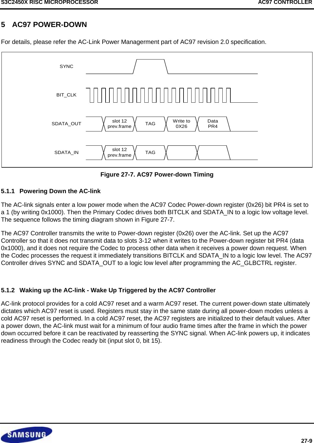
![S3C2450X RISC MICROPROCESSOR AC97 CONTROLLER 27-13 8.2 AC97 GLOBAL CONTROL REGISTER (AC_GLBCTRL) This is the global register of the AC97 controller. There are interrupt control registers, DMA control registers, AC-Link control register, data transmission control register and related reset control register. Register Address R/W Description Reset ValueAC_GLBCTRL 0x5B000000 R/W AC97 Global Control Register 0x000000 AC_GLBCTRL Bit Description Initial State- [31:23] Reserved. 0 Codec ready interrupt enable [22] 0 = Disable 1 = Enable 0 PCM out channel underrun interrupt enable [21] 0 = Disable 1 = Enable ( FIFO is empty) 0 PCM in channel overrun interrupt enable [20] 0 = Disable 1 = Enable ( FIFO is full) 0 Mic in channel overrun interrupt enable [19] 0 = Disable 1 = Enable ( FIFO is full) 0 PCM out channel threshold interrupt enable [18] 0 = Disable 1 = Enable ( FIFO is half empty) 0 PCM in channel threshold interrupt enable [17] 0 = Disable 1 = Enable ( FIFO is half full) 0 MIC in channel threshold interrupt enable [16] 0 = Disable 1 = Enable ( FIFO is half full) 0 - [15:14] Reserved. 00 PCM out channel transfer mode [13:12] 00 = Off 01 = PIO 10 = DMA 11 = Reserved 00 PCM in channel transfer mode [11:10] 00 = Off 01 = PIO 10 = DMA 11 = Reserved 00 MIC in channel transfer mode [9:8] 00 = Off 01 = PIO 10 = DMA 11 = Reserved 00 - [7:4] Reserved. 0000 Transfer data enable using AC-link [3] 0 = Disable 1 = Enable 0 AC-Link on [2] 0 = Off 1 = SYNC signal transfer to Codec 0 Warm reset [1] 0 = Normal 1 = Wake up codec from power down 0 Cold reset [0] 0 = Normal (note 2) 1 = Reset Codec and Controller Registers (note 1) 0 NOTES: 1. During Cold reset, writing to any AC97 Registers will not affected. 2. When recovering from Cold reset, writing to any AC97 Registers will not be affected. Example: For consecutive Cold reset and Warm reset, first set AC_GLBCTRL=0x1 then set AC_GLBCTRL=0x0. After recovering from cold reset set AC_GLBCTRL=0x2 then AC_GLBCTRL=0x0.](https://usermanual.wiki/Diasonic-Technology-Co/RVM-704M.Users-Manual/User-Guide-1826140-Page-739.png)
![AC97 CONTROLLER S3C2450X RISC MICROPROCESSOR 27-14 8.3 AC97 GLOBAL STATUS REGISTER (AC_GLBSTAT) This is the status register. When the interrupt is occurred, you can check what the interrupt source is. Register Address R/W Description Reset ValueAC_GLBSTAT 0x5B000004 R AC97 Global Status Register 0x00000001 AC_GLBSTAT Bit Description Initial State- [31:23] Reserved. 0x00 Codec ready interrupt [22] 0 = Not requested 1 = Requested 0 PCM out channel underrun interrupt [21] 0 = Not requested 1 = Requested 0 PCM in channel overrun interrupt [20] 0 = Not requested 1 = Requested 0 MIC in channel overrun interrupt [19] 0 = Not requested 1 = Requested 0 PCM out channel threshold interrupt [18] 0 = Not requested 1 = Requested 0 PCM in channel threshold interrupt [17] 0 = Not requested 1 = Requested 0 MIC in channel threshold interrupt [16] 0 = Not requested 1 = Requested 0 - [15:3] Reserved. 0x000 Controller main state [2:0] 000 = Idle 001 = Init 010 = Ready 011 = Active 100 = LP 101 = Warm 001 8.4 AC97 CODEC COMMAND REGISTER (AC_CODEC_CMD) When you control writing or reading, you must set the Read enable bit, If you want to write data to the AC97 Codec, you set the index(or address) of the AC97 Codec and data. Register Address R/W Description Reset ValueAC_CODEC_CMD 0x5B000008 R/W AC97 Codec Command Register 0x00000000 AC_CODEC_CMD Bit Description Initial State- [31:24] Reserved 0x00 Read enable [23] 0 = Command write (note) 1 = Status read 0 Address [22:16] Codec command address 0x00 Data [15:0] Codec command data 0x0000 NOTE: When the commands are written on the AC_CODDEC_CMD register, It is recommended that the delay time between the command and the next command is more than 1 / 48kHz.](https://usermanual.wiki/Diasonic-Technology-Co/RVM-704M.Users-Manual/User-Guide-1826140-Page-740.png)
![S3C2450X RISC MICROPROCESSOR AC97 CONTROLLER 27-15 8.5 AC97 CODEC STATUS REGISTER (AC_CODEC_STAT) If the Read enable bit is 1 and Codec command address is valid, Codec status data is also valid. Register Address R/W Description Reset ValueAC_CODEC_STAT 0x5B00000C R AC97 Codec Status Register 0x00000000 AC_CODEC_STAT Bit Description Initial State- [31:23] Reserved. 0x00 Address [22:16] Codec status address 0x00 Data [15:0] Codec status data 0x0000 NOTES: If you want to read data from AC97 codec register via the AC_CODDEC_STAT register, you should follow the steps. 1. Write command address and data on the AC_CODEC_CMD register with Bit[23] =1. 2. Have a delay time. 3. Read command address and data from AC_CODEC_STAT register. 8.6 AC97 PCM OUT/IN CHANNEL FIFO ADDRESS REGISTER (AC_PCMADDR) To index the internal PCM FIFOs address. Register Address R/W Description Reset ValueAC_PCMADDR 0x5B000010 R AC97 PCM Out/In Channel FIFO Address Register 0x00000000 AC_PCMADDR Bit Description Initial State- [31:28] Reserved. 0000 Out read address [27:24] PCM out channel FIFO read address 0000 - [23:20] Reserved. 0000 In read address [19:16] PCM in channel FIFO read address 0000 - [15:12] Reserved. 0000 Out write address [11:8] PCM out channel FIFO write address 0000 - [7:4] Reserved. 0000 In write address [3:0] PCM in channel FIFO write address 0000](https://usermanual.wiki/Diasonic-Technology-Co/RVM-704M.Users-Manual/User-Guide-1826140-Page-741.png)
![AC97 CONTROLLER S3C2450X RISC MICROPROCESSOR 27-16 8.7 AC97 MIC IN CHANNEL FIFO ADDRESS REGISTER (AC_MICADDR) To index the internal MIC-in FIFO address. Register Address R/W Description Reset ValueAC_MICADDR 0x5B000014 R AC97 MIC In Channel FIFO Address Register 0x00000000 AC_MICADDR Bit Description Initial State- [31:20] Reserved. 0000 Read address [19:16] MIC in channel FIFO read address 0000 - [15:4] Reserved. 0x000 Write address [3:0] MIC in channel FIFO write address 0000 8.8 AC97 PCM OUT/IN CHANNEL FIFO DATA REGISTER (AC_PCMDATA) This is PCM out/in channel FIFO data register. Register Address R/W Description Reset ValueAC_PCMDATA 0x5B000018 R/W AC97 PCM Out/In Channel FIFO Data Register 0x00000000 AC_PCMDATA Bit Description Initial StateRight data [31:16] PCM out/in right channel FIFO data Read = PCM in right channel Write = PCM out right channel 0x0000 Left data [15:0] PCM out/in left channel FIFO data Read = PCM in left channel Write = PCM out left channel 0x0000 8.9 AC97 MIC IN CHANNEL FIFO DATA REGISTER (AC_MICDATA) This is MIC-in channel FIFO data register. Register Address R/W Description Reset ValueAC_MICDATA 0x5B00001C R AC97 MIC In Channel FIFO Data Register 0x00000000 AC_MICDATA Bit Description Initial State- [31:16] Reserved 0x0000 Mono data [15:0] MIC in mono channel FIFO data 0x0000](https://usermanual.wiki/Diasonic-Technology-Co/RVM-704M.Users-Manual/User-Guide-1826140-Page-742.png)
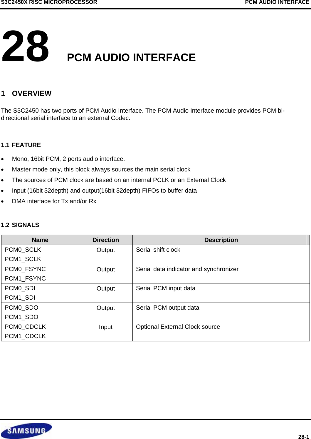
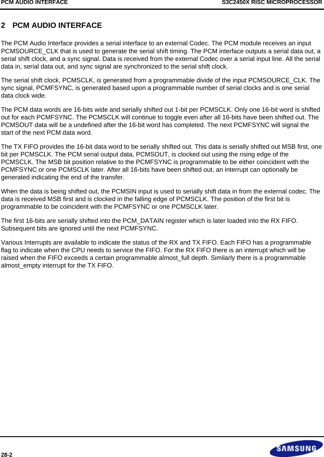
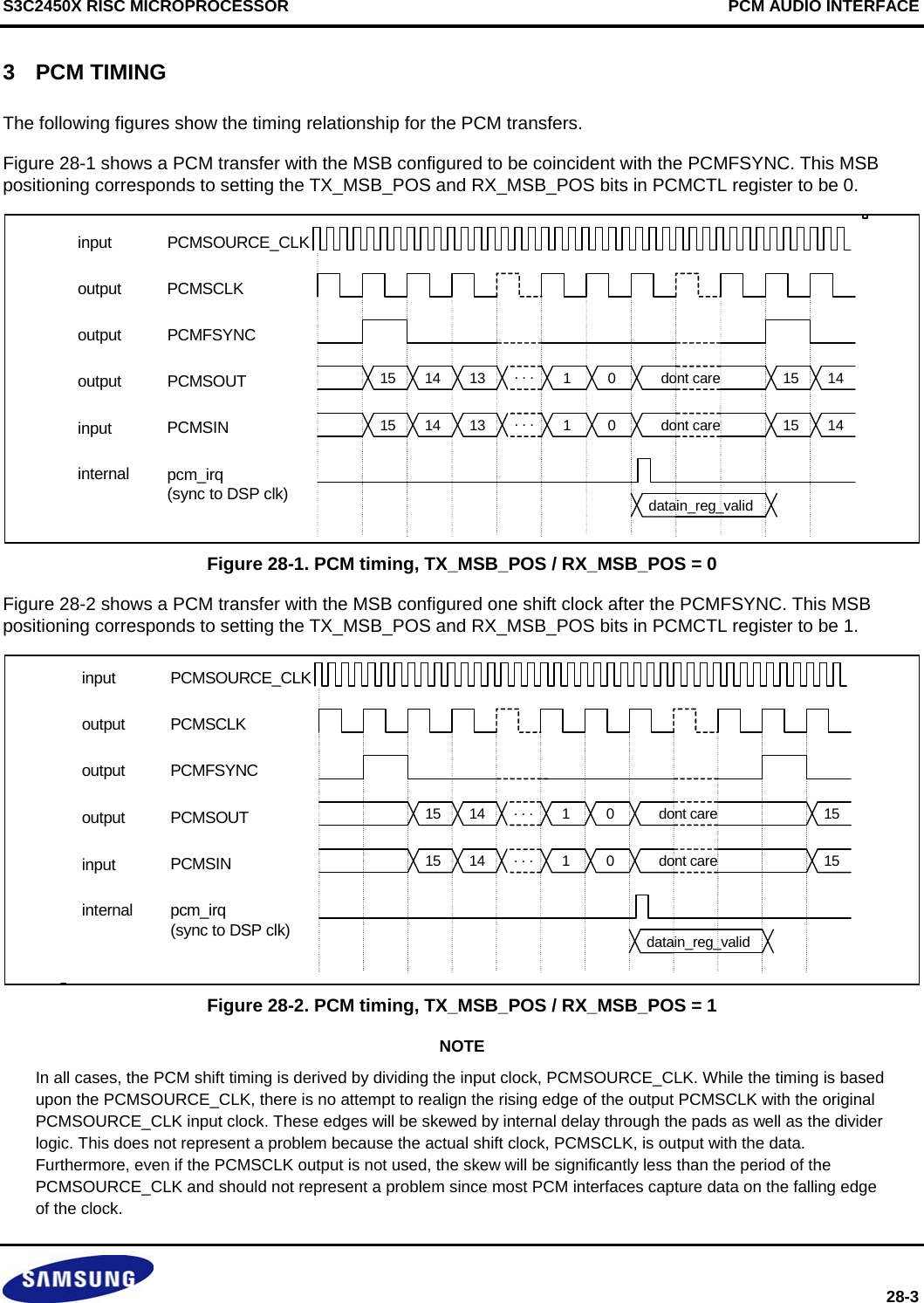
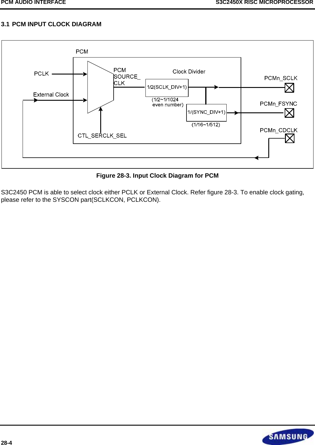
![PCM AUDIO INTERFACE S3C2450X RISC MICROPROCESSOR 28-6 3.4 PCM CONTROL REGISTER The PCM_CTL register is used to control the various aspects of the PCM module. It also provides a status bit to provide the option to using polling instead of interrupt based control. Register Address R/W Description Reset ValuePCM_CTL0 0x5C000000 R/W Control the PCM0 Audio Interface 0x00000000PCM_CTL1 0x5C000100 R/W Control the PCM1 Audio Interface 0x00000000 The bit definitions for the PCM_CTL Control Register are shown below: PCM_CTLn Bit Description Initial StateReserved [31:19] Reserved TXFIFO_DIPSTICK [18:13] Determines when the almost_full, almost_empty flags go active for the TXFIFO TXFIFO_ALMOST_EMPTY: txfifo_depth < txfifo_dipstick TXFIFO_ALMOST_FULL: txfifo_depth > (32 – txfifo_dipstick) Note: - If txfifo_dipstick is 0, Almost_empty, Almost_full are invalid - For DMA loading of TX fifo, Txfifo_dipstick should be equal to 2 or greater than 2(txfifo_dipstick >= 2) This is required since the PCM_TXDMA uses TXFIFO_ALMOST_FULL as the DMA request (keep requesting data until the FIFO is almost full) In some circumstances, the DMA write one more word after the DMA_req goes away. Thus the almost_full flag most go active with at least space for one extra word in the fifo 0 RXFIFO_DIPSTICK [12:7] Determines when the almost_full, almost_empty flags go active for the RXFIFO RXFIFO_ALMOST_EMPTY : fifo_depth < fifo_dipstick RXFIFO_ALMOST_FULL : fifo_depth > (32 – fifo_dipstick) Note: - If fifo_dipstick is 0, Almost_empty, Almost_full are invalid. - For DMA, RXFIFO_DIPSTICK is a don’t care. (DMA unloading of RX fifo uses the RXFIFO_EMPTY flag as the DMA request) - Non-DMA IRQ/polling RXFIFO_DIPSTICK should be 32. This will have the effect of RXFIFO_ALMOST_FULL acting as a rx_fifo_not_empty flag (as a not RXFIFO_EMPTY). 0 PCM_TX_DMA_EN [6] Enable the DMA interface for the TXFIFO DMA must operate in the demand mode. DMA_TX request will occur whenever the TXFIFO is not almost full 0 PCM_RX_DMA_EN [5] Enable the DMA interface for the RXFIFO DMA must operate in the demand mode. 0](https://usermanual.wiki/Diasonic-Technology-Co/RVM-704M.Users-Manual/User-Guide-1826140-Page-748.png)
![S3C2450X RISC MICROPROCESSOR PCM AUDIO INTERFACE 28-7 PCM_CTLn Bit Description Initial StateDMA_RX request will occur whenever the RXFIFO is not empty. TX_MSB_POS [4] Controls the position of the MSB bit in the serial output stream relative to the PCMFSYNC signal 0 = MSB sent during the same clock that PCMFSYNC is high 1 = MSB sent on the next PCMSCLK cycle after PCMFSYNC is high 0 RX_MSB_POS [3] Controls the position of the MSB bit in the serial input stream relative to the PCMFSYNC signal 0 = MSB is captured on the falling edge of PCMSCLK during the same cycle that PCMFSYNC is high 1 = MSB is captured on the falling edge of PCMSCLK during the cycle after the PCMFSYNC is high 0 PCM_TXFIFO_EN [2] Enable the TXFIFO (note 1) 0 PCM_RXFIFO_EN [1] Enable the RXFIFO (note 1) 0 PCM_PCM_ENABLE [0] PCM enable signal. 1 = Enables the serial shift state machines. (note 2) The enable must be set HIGH for the PCM to operate. 0 = The PCMSOUT will not toggle. The internal divider-counters (serial shift register’s counter) are held in reset. (note 3) 0 NOTES: 1. To flush FIFO, first set PCM_TX/RXFIFO_EN =0x0 then set PCM_TX/RXFIFO_EN =0x1. 2. To Start PCM operation please refer the following steps - PCM_TXFIFO_EN=0x1; - PCM_TX_DMA_EN=0x1; - wait until fifo full - CTL_SERCLK_EN =0x1; - PCM_PCM_ENABLE = 0x1; 3. To pause PCM operation, with CTL_SERCLK_EN = 0x0, PCM_PCM_ENABLE bit should be set to zero.](https://usermanual.wiki/Diasonic-Technology-Co/RVM-704M.Users-Manual/User-Guide-1826140-Page-749.png)
![PCM AUDIO INTERFACE S3C2450X RISC MICROPROCESSOR 28-8 3.5 PCM CLK CONTROL REGISTER Register Address R/W Description Reset ValuePCM_CLKCTL0 0x5C000004 R/W Control the PCM0 Audio Inteface 0x00000000PCM_CLKCTL1 0x5C000104 R/W Control the PCM1 Audio Inteface 0x00000000 The bit definitions for the PCM_CTL Control Register are shown below: PCM_CLKCTLn Bit Description Initial StateReserved [31:20] Reserved CTL_SERCLK_EN [19] Enable the serial clock division logic. Must be HIGH for the PCM to operate (if it is high, PCMSCLK and PCMFSYNC is operated.) 1) 0 CTL_SERCLK_SEL [18] Select the source of the PCMSOURCE_CLK 0 = External clock 1 = PCLK 0 SCLK_DIV [17:9] Controls the divider used to create the PCMSCLK based on the PCMSOURCE_CLK. (1/2~1/1024) PCMSLCK will be PCMSOURCE_CLK / 2*(SCLK_DIV+1) 000 SYNC_DIV [8:0] Controls the frequency of the PCMFSYNC signal based on the PCMSCLK. (1/1~1/512) Freq. of PCMFSYNC = Freq. of PCMSCLK/(SYNC_DIV+1) 000 NOTE: For correct functioning of PCM pause and continue, please refer following steps. To Pause PCM operation, first set CTL_SERCLK_EN = 0x0, then set PCM_PCM_ENABLE =0x0. To continue PCM operation, first set CTL_SERCLK_EN = 0x1, then set PCM_PCM_ENABLE =0x1.](https://usermanual.wiki/Diasonic-Technology-Co/RVM-704M.Users-Manual/User-Guide-1826140-Page-750.png)
![S3C2450X RISC MICROPROCESSOR PCM AUDIO INTERFACE 28-9 3.6 THE PCM TX FIFO REGISTER Register Address R/W Description Reset ValuePCM_TXFIFO0 0x5C000008 R/W PCM0 interface Transmit FIFO data register 0x00010000PCM_TXFIFO1 0x5C000108 R/W PCM1 interface Transmit FIFO data register 0x00010000 The bit definitions for the PCM_TXFIFO Register are shown below: PCM_TXFIFOn Bit Description Initial StateReserved [31:17] Reserved TXFIFO_DVALID [16] TXFIFO data is valid Write: don’t care Read: TXFIFO read data valid 1 = Valid 0 = Invalid (probably read an empty fifo) 1 TXFIFO_DATA [15:0] Write: Write PCM data to TXFIFO Note: The TXFIFO is read by the PCM serial shift engine Read: Read PCM data from TXFIFO for supporting debug TXFIFO 0](https://usermanual.wiki/Diasonic-Technology-Co/RVM-704M.Users-Manual/User-Guide-1826140-Page-751.png)
![PCM AUDIO INTERFACE S3C2450X RISC MICROPROCESSOR 28-10 3.7 PCM RX FIFO REGISTER Register Address R/W Description Reset ValuePCM_RXFIFO0 0x5C00000C R/W PCM0 interface Receive FIFO data register 0x00010000PCM_RXFIFO1 0x5C00010C R/W PCM1 interface Receive FIFO data register 0x00010000 The bit definitions for the PCM_RXFIFO Register are shown below: PCM_RXFIFOn Bit Description Initial State Reserved [31:17] Reserved RXFIFO_DVALID [16] RXFIFO data is valid Write: don’t care Read: TXFIFO read data valid 1 = Valid 0 = Invalid (probably read an empty fifo) 1 RXFIFO_DATA [15:0] Write: Write PCM data to RXFIFO for debugging RXFIFO Read: Read PCM data from RXFIFO Note: The RXFIFO is written by the PCM serial shift engine 0](https://usermanual.wiki/Diasonic-Technology-Co/RVM-704M.Users-Manual/User-Guide-1826140-Page-752.png)
![S3C2450X RISC MICROPROCESSOR PCM AUDIO INTERFACE 28-11 3.8 PCM INTERRUPT CONTROL REGISTER The PCM_IRQ_CTL register is used to control the various aspects of the PCM interrupts. Register Address R/W Description Reset Value PCM_IRQ_CTL0 0x5C000010 R/W Control the PCM0 Interrupts 0x00000000 PCM_IRQ_CTL1 0x5C000110 R/W Control the PCM1 Interrupts 0x00000000 The bit definitions for the PCM_IRQ_CTL Control Register are shown below: PCM_IRQ_CTLn Bit Description Initial StateReserved [31:15] Reserved EN_IRQ_TO_ARM [14] Controls whether the PCM interrupt is sent to the ARM or not 1: PCM IRQ is forwarded to the ARM subsystem 0: PCM IRQ is NOT forwarded to the ARM subsystem 0 Reserved [13] Reserved 0 TRANSFER_DONE [12] Interrupt is generated every time the serial shift for a 16bit PCM Data word completes 1: IRQ source enabled 0: IRQ source disabled 0 TXFIFO_EMPTY [11] Interrupt is generated whenever the TxFIFO is empty 1: IRQ source enabled 0: IRQ source disabled 0 TXFIFO_ALMOST_ EMPTY [10] Interrupt is generated whenever the TxFIFO is ALMOST_EMPTY which is defined as TX_FIFO_DEPTH < TX_FIFO_DIPSTICK 1: IRQ source enabled 0: IRQ source disabled 0 TXFIFO_FULL [9] Interrupt is generated whenever the TxFIFO is full 1: IRQ source enabled 0: IRQ source disabled 0 TXFIFO_ALMOST_FULL [8] Interrupt is generated whenever the TxFIFO is ALMOST_FULL which is defined as TX_FIFO_DEPTH > (32 – TX_FIFO_DIPSTICK) 1: IRQ source enabled 0: IRQ source disabled 0](https://usermanual.wiki/Diasonic-Technology-Co/RVM-704M.Users-Manual/User-Guide-1826140-Page-753.png)
![PCM AUDIO INTERFACE S3C2450X RISC MICROPROCESSOR 28-12 PCM_IRQ_CTLn Bit Description Initial StateTXFIFO_ERROR_ STARVE [7] Interrupt is generated for TxFIFO starve ERROR. This occurs whenever the TxFIFO is read when it is still empty. This is considered an ERROR and will have unexpected results 1: IRQ source enabled 0: IRQ source disabled 0 TXFIFO_ERROR_ OVERFLOW [6] Interrupt is generated for TxFIFO overflow ERROR. This occurs whenever the TxFIFO is written when it is already full. This is considered an ERROR and will have unexpected results 1: IRQ source enabled 0: IRQ source disabled 0 RXFIFO_EMPTY [5] Interrupt is generated whenever the RxFIFO is empty 1: IRQ source enabled 0: IRQ source disabled 0 RXFIFO_ALMOST_ EMPTY [4] Interrupt is generated whenever the RxFIFO is ALMOST_EMPTY which is defined as RX_FIFO_DEPTH < RX_FIFO_DIPSTICK 1: IRQ source enabled 0: IRQ source disabled 0 RX_FIFO_FULL [3] Interrupt is generated whenever the RxFIFO is full 1: IRQ source enabled 0: IRQ source disabled 0 RX_FIFO_ALMOST_ FULL [2] Interrupt is generated whenever the RxFIFO is ALMOST_FULL which is defined as RX_FIFO_DEPTH > (32 – RX_FIFO_DIPSTICK) 1: IRQ source enabled 0: IRQ source disabled 0 RXFIFO_ERROR_STARVE [1] Interrupt is generated for RxFIFO starve ERROR. This occurs whenever the RxFIFO is read when it is still empty. This is considered an ERROR and will have unexpected results 1: IRQ source enabled 0: IRQ source disabled 0](https://usermanual.wiki/Diasonic-Technology-Co/RVM-704M.Users-Manual/User-Guide-1826140-Page-754.png)
![S3C2450X RISC MICROPROCESSOR PCM AUDIO INTERFACE 28-13 PCM_IRQ_CTLn Bit Description Initial StateRXFIFO_ERROR_ OVERFLOW [0] Interrupt is generated for RxFIFO overflow ERROR. This occurs whenever the RxFIFO is written when it is already full. This is considered an ERROR and will have unexpected results 1: IRQ source enabled 0: IRQ source disabled 0](https://usermanual.wiki/Diasonic-Technology-Co/RVM-704M.Users-Manual/User-Guide-1826140-Page-755.png)
![PCM AUDIO INTERFACE S3C2450X RISC MICROPROCESSOR 28-14 3.9 PCM INTERRUPT STATUS REGISTER The PCM_IRQ_STAT register is used to report IRQ status. Register Address R/W Description Reset ValuePCM_IRQ_STAT0 0x5C000014 R PCM0 Interrupt Status 0x00000000PCM_IRQ_STAT1 0x5C000114 R PCM1 Interrupt Status 0x00000000 The bit definitions for the PCM_IRQ_STATUS Register are described below: PCM_IRQ_STATn Bit Description Initial StateReserved [31:14] Reserved IRQ_PENDING [13] Monitoring PCM IRQ. 1 = PCM IRQ is occurred. 0 = PCM IRQ is not occurred. 0 TRANSFER_DONE [12] Interrupt is generated every time the serial shift for a word completes 1 = IRQ is occurred. 0 = IRQ is not occurred. 0 TXFIFO_EMPTY [11] Interrupt is generated whenever the TX FIFO is empty 1 = IRQ is occurred. 0 = IRQ is not occurred. 0 TXFIFO_ALMOST _EMPTY [10] Interrupt is generated whenever the TxFIFO is ALMOST empty. 1 = IRQ is occurred. 0 = IRQ is not occurred. 0 TXFIFO_FULL [9] Interrupt is generated whenever the TX FIFO is full 1 = IRQ is occurred. 0 = IRQ is not occurred. 0 TXFIFO_ALMOST _FULL [8] Interrupt is generated whenever the TX FIFO is ALMOST full. 1 = IRQ is occurred. 0 = IRQ is not occurred. 0 TXFIFO_ERROR _STARVE [7] Interrupt is generated for TX FIFO starve ERROR. This occurs whenever the TX FIFO is read when it is still empty. This is considered as an ERROR and will have unexpected results 1 = IRQ is occurred. 0 = IRQ is not occurred. 0](https://usermanual.wiki/Diasonic-Technology-Co/RVM-704M.Users-Manual/User-Guide-1826140-Page-756.png)
![S3C2450X RISC MICROPROCESSOR PCM AUDIO INTERFACE 28-15 PCM_IRQ_STATn Bit Description Initial StateTXFIFO_ERROR _OVERFLOW [6] Interrupt is generated for TX FIFO overflow ERROR. This occurs whenever the TX FIFO is written when it is already full. This is considered as an ERROR and will have unexpected results 1 = IRQ is occurred. 0 = IRQ is not occurred. 0 RXFIFO_EMPTY [5] Interrupt is generated whenever the RX FIFO is empty 1 = IRQ is occurred. 0 = IRQ is not occurred. 0 RXFIFO_ALMOST _EMPTY [4] Interrupt is generated whenever the RX FIFO is ALMOST empty. 1 = IRQ is occurred. 0 = IRQ is not occurred. 0 RX_FIFO_FULL [3] Interrupt is generated whenever the RX FIFO is full 1 = IRQ is occurred. 0 = IRQ is not occurred. 0 RX_FIFO_ALMOST _FULL [2] Interrupt is generated whenever the RX FIFO is ALMOST full. 1 = IRQ is occurred. 0 = IRQ is not occurred. 0 RXFIFO_ERROR _STARVE [1] Interrupt is generated for RX FIFO starve ERROR. This occurs whenever the RX FIFO is read when it is still empty. This is considered as an ERROR and will have unexpected results 1 = IRQ is occurred. 0 = IRQ is not occurred. 0 RXFIFO_ERROR _OVERFLOW [0] Interrupt is generated for RX FIFO overflow ERROR. This occurs whenever the RX FIFO is written when it is already full. This is considered as an ERROR and will have unexpected results 1 = IRQ is occurred. 0 = IRQ is not occurred. 0 NOTE: More than one interrupt sources(which was set by PCM_IRQ_CTL register) can cause interrupt, at same time(i.e, interrupt at PCM is OR-ed interrupt.) So in Interrupt Service Routine, user should check this register bits which you set as interrupt sources.](https://usermanual.wiki/Diasonic-Technology-Co/RVM-704M.Users-Manual/User-Guide-1826140-Page-757.png)
![PCM AUDIO INTERFACE S3C2450X RISC MICROPROCESSOR 28-16 3.10 PCM FIFO STATUS REGISTER The PCM_FIFO_STAT register is used to report FIFO status. Register Address R/W Description Reset ValuePCM_FIFO_STAT0 0x5C000018 R PCM0 FIFO Status 0x00000000PCM_FIFO_STAT1 0x5C000118 R PCM1 FIFO Status 0x00000000 The bit definitions for the PCM_FIFO_STATUS Register are shown below: PCM_FIFO_STATn Bit Description Initial StateReserved [31:20] Reserved TXFIFO_COUNT [19:14] TX FIFO data count(0 ~ 32). 0 TXFIFO_EMPTY [13] 1 = TXFIFO is empty 0 = TXFIFO is not empty 0 TXFIFO_ALMOST_EMPTY [12] 1 = TXFIFO is ALMOST_EMPTY 0 = TXFIFO is not ALMOST_EMPTY 0 TXFIFO_FULL [11] 1 = TXFIFO is full 0 = TXFIFO is not full 0 TXFIFO_ALMOST_FULL [10] 1 = TXFIFO is ALMOST_FULL 0 = TXFIFO is not ALMOST_FULL 0 RXFIFO_COUNT [9:4] RX FIFO data count(0 ~ 32). RXFIFO_EMPTY [3] 1 = RXFIFO is empty 0 = RXFIFO is not empty 0 RXFIFO_ALMOST_EMPTY [2] 1 = RXFIFO is ALMOST_EMPTY 0 = RXFIFO is not ALMOST_EMPTY 0 RX_FIFO_FULL [1] 1 = RXFIFO is full 0 = RXFIFO is not full 0 RX_FIFO_ALMOST_FULL [0] 1 = RXFIFO is ALMOST_FULL 0 = RXFIFO is not ALMOST_FULL 0](https://usermanual.wiki/Diasonic-Technology-Co/RVM-704M.Users-Manual/User-Guide-1826140-Page-758.png)
![S3C2450X RISC MICROPROCESSOR PCM AUDIO INTERFACE 28-17 3.11 PCM INTERRUPT CLEAR REGISTER The PCM_CLRINT register is used to clear the interrupt. Interrupt service routine is responsible for clearing interrupt asserted. Writing any values on this register clears interrupts for ARM. Reading this register is not allowed. Clearing interrupt must be prior to resolving the interrupt condition, otherwise another interrupt that would occur after this interrupt may be ignored. Register Address R/W Description Reset ValuePCM_CLRINT0 0x5C000020 W PCM0 INTERRUPT CLEAR - PCM_CLRINT1 0x5C000120 W PCM1 INTERRUPT CLEAR The bit definitions for the PCM_CLRINT Register are shown below: PCM_CLRINTn Bit Description Initial StateReserved [31:1] Reserved 0 CLRINT [0] Interrupt register clear 0](https://usermanual.wiki/Diasonic-Technology-Co/RVM-704M.Users-Manual/User-Guide-1826140-Page-759.png)

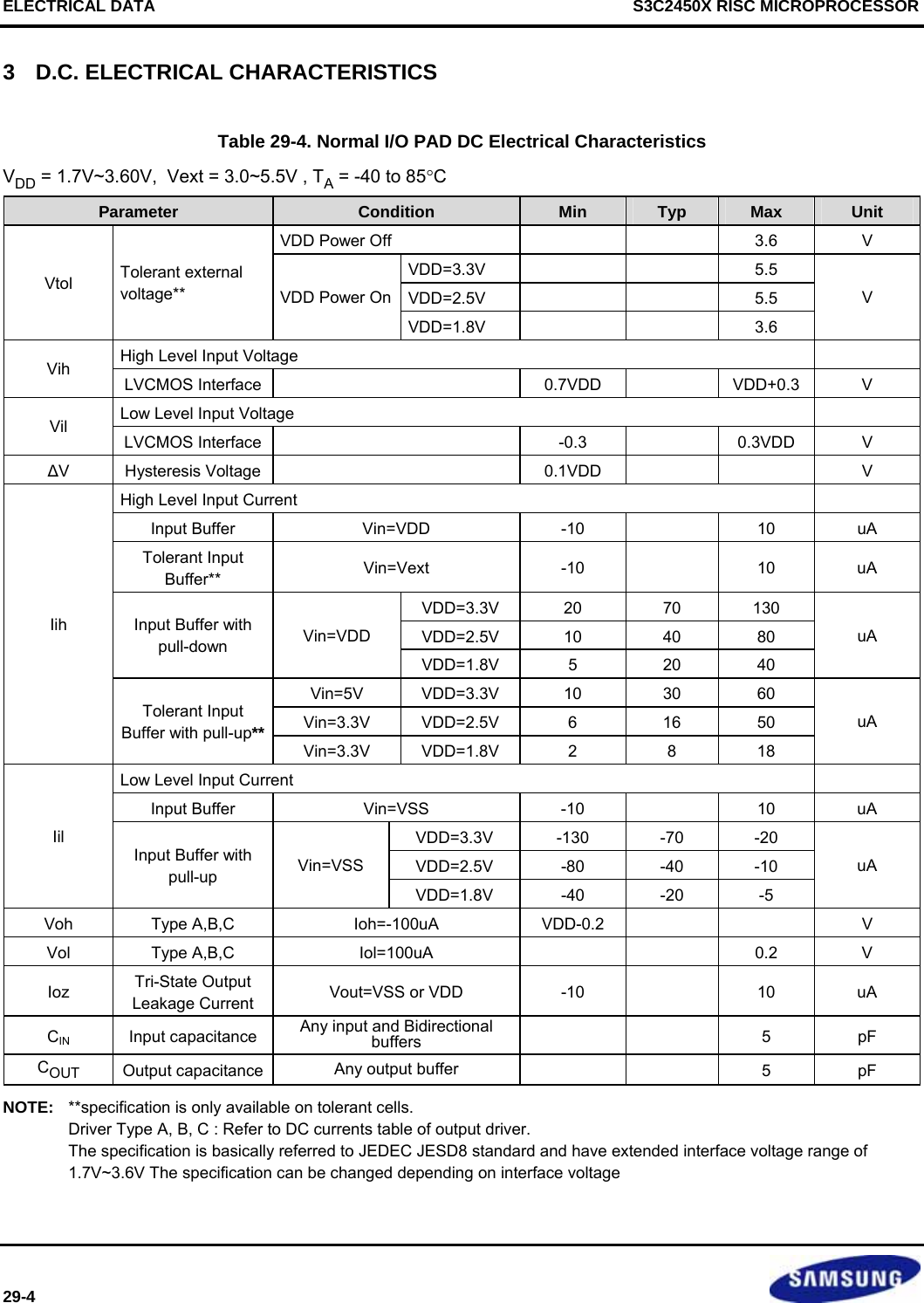
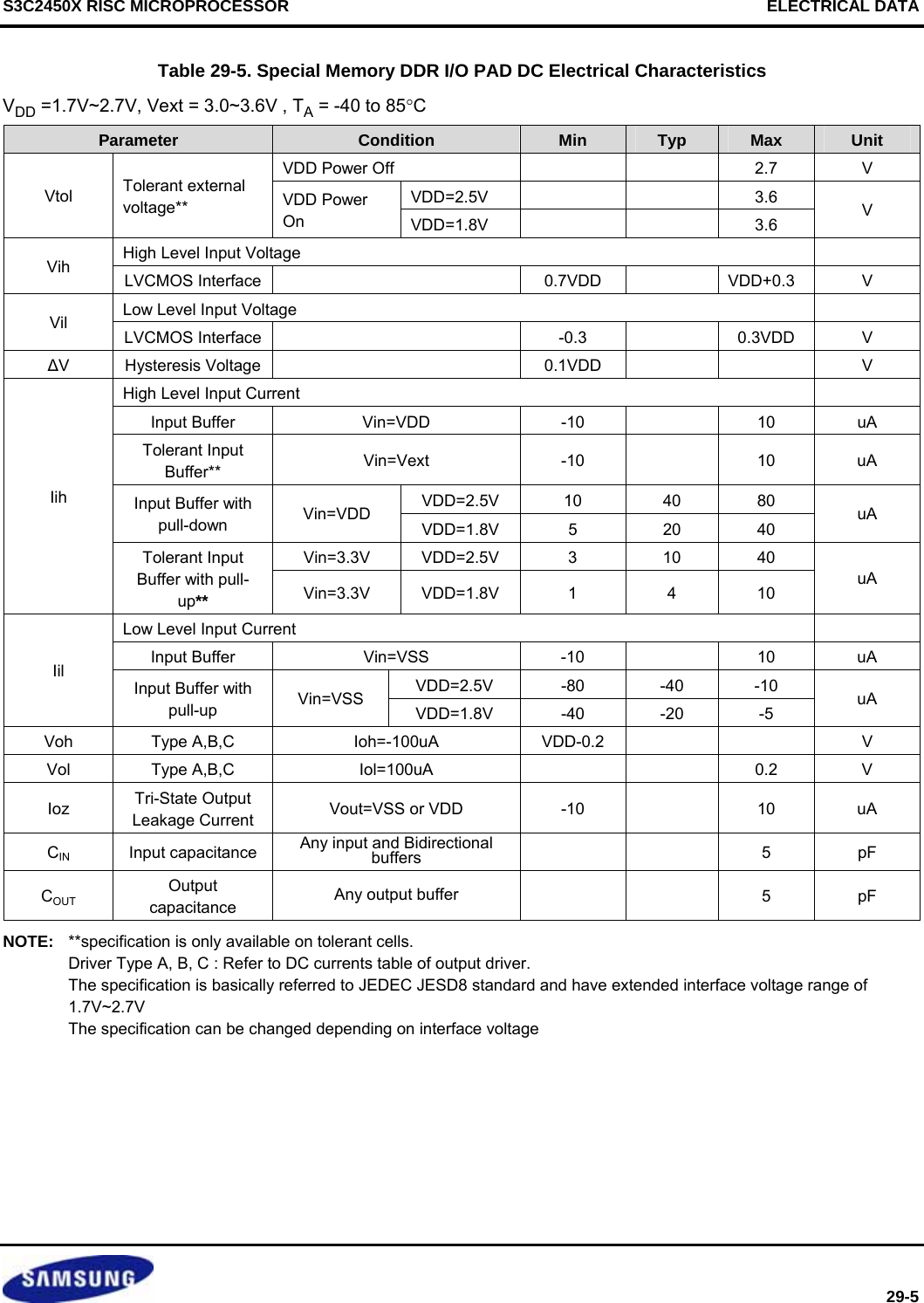
![ELECTRICAL DATA S3C2450X RISC MICROPROCESSOR 29-6 Table 29-6. USB DC Electrical Characteristics VDD = 3.0 to 3.6V; GND = 0V; Cload = 2uF; unless otherwise specified. Symbol Parameter Conditions Min Typ Max Unit VDD Supply voltage 3.0 3.3 3.6 V VDI Differential input sensitivity 0.2 V VCM Differential common mode voltage 0.8 2.5 V VIL Low level input voltage 0.8 V VIH High level input voltage 2.0 V VOL Low level output voltage RL = 1.5KΩ to +3.6V 0.3 V VOH High level output voltage RL = 15KΩ to GND 2.8 3.6 V ILZ Tri-state leakage current -10 10 uA Cin Transceiver capacitance Pin to GND 10 pF RPD Pull down resistance on pins DP/DM Enable internal resistors 10 20 kΩ RPU Pull up resistance on DP Enable internal resistor 1 2 kΩ ZDRV Driver output impedance Steady-state drive[1] 39 44 Ω ZINP Input impedance 10 MΩVTERM Termination voltage for upstream port pull up 3.0 3.6 V Table 29-7. RTC OSC DC Electrical Characteristics Symbol Parameter Min Typ Max Unit VDD_RTC Output supply voltage 1.7 2.5 3.6 V VIH DC input logic high 0.7*VDDrtc V VIL DC input logic low 0.3*VDDrtc V IIH High level input current -10 10 μA IIL Low level input current -10 10 μA](https://usermanual.wiki/Diasonic-Technology-Co/RVM-704M.Users-Manual/User-Guide-1826140-Page-766.png)
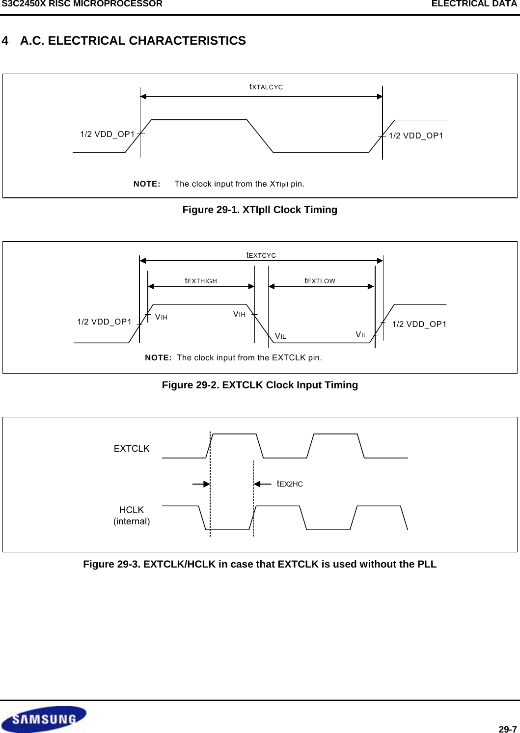
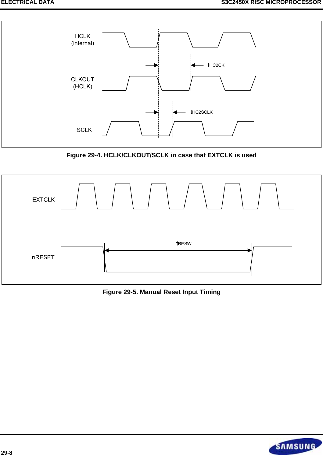
![S3C2450X RISC MICROPROCESSOR ELECTRICAL DATA 29-9 nRESETXTIpll orEXTCLKVCOoutputMCU operates by XTIpll or EXTCLK clcok.ClockDisabletPLLFCLK is new frequency.PowerPLL can operate after OM[3:2] is latched.PLL is configured by S/W first time.VCO is adapted to new clock frequency.FCLK.........tRST2RUN Figure 29-6. Power-On Oscillation Setting Timing](https://usermanual.wiki/Diasonic-Technology-Co/RVM-704M.Users-Manual/User-Guide-1826140-Page-769.png)
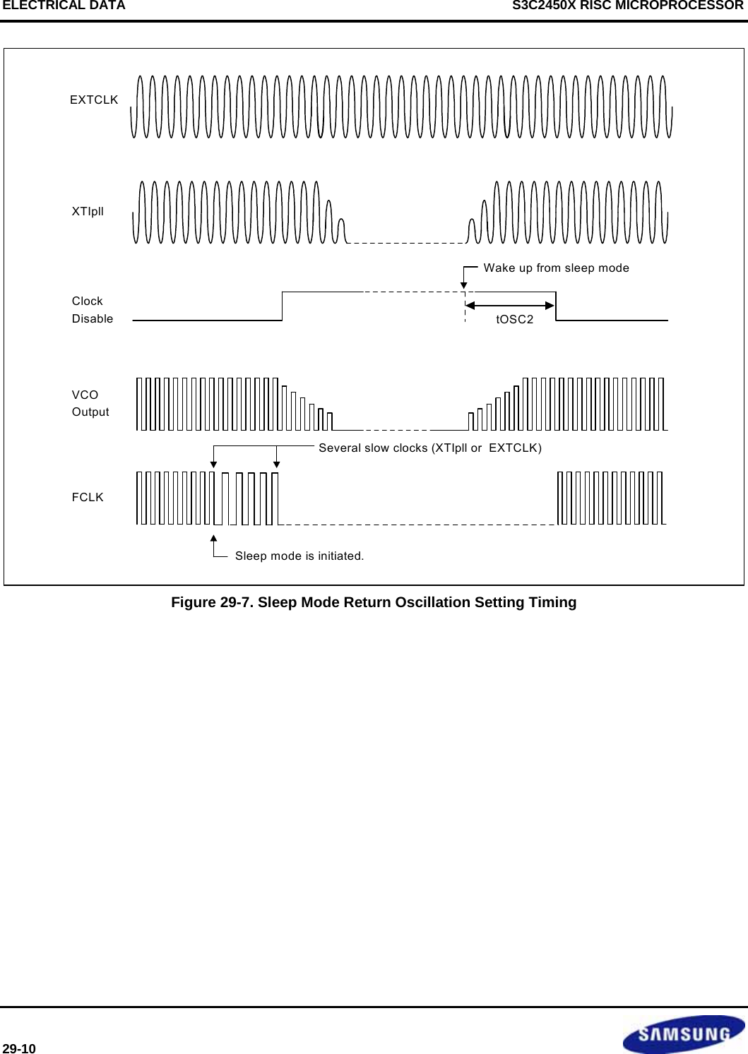
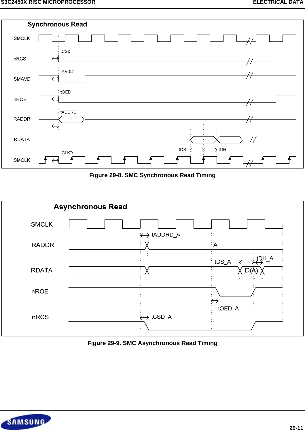
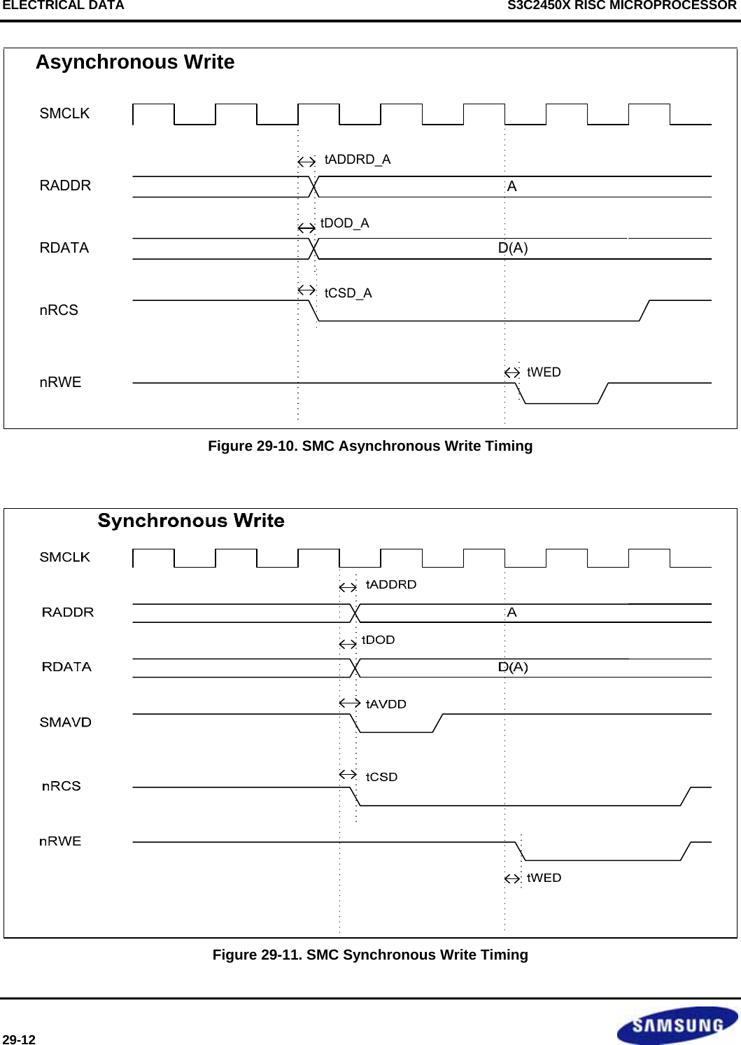
![S3C2450X RISC MICROPROCESSOR ELECTRICAL DATA 29-13 RADDR[26:0]RDATA[31:0]nRCSnROEnWAITAD(A)SMCLKtWS tHS Figure 29-12. SMC Wait Timing](https://usermanual.wiki/Diasonic-Technology-Co/RVM-704M.Users-Manual/User-Guide-1826140-Page-773.png)
![ELECTRICAL DATA S3C2450X RISC MICROPROCESSOR 29-14 TACLS TWRPH0 TWRPH1COMMANDTWRPH0 TWRPH1ADDRESSRDATA[15:0]HCLKFCLEnFWEtCLED tCLEDtWED tWEDtWDDtWDDtALEDtWEDtALEDtWEDtWDDTACLStWDDTWRPH0 TWRPH1ADDRESStWDDtALEDtWEDtALEDtWEDtWDDTACLS<Nand booting> <After Nand booting>HCLKnFWETWRPH0 TWRPH1HCLKnFRETWRPH0 TWRPH1RDATAtWEDtWEDtWDDtREDtREDtRDStRDHtWDDWDATARDATA[15:0]HCLKFALEnFWERDATA[15:0]HCLKFALEnFWE Figure 29-13. Nand Flash Timing](https://usermanual.wiki/Diasonic-Technology-Co/RVM-704M.Users-Manual/User-Guide-1826140-Page-774.png)
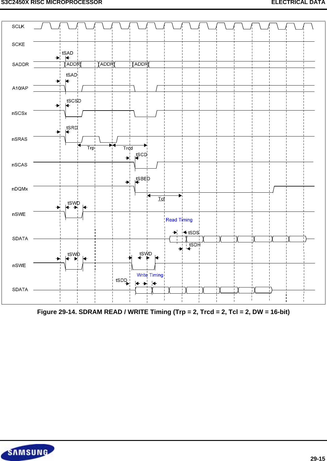
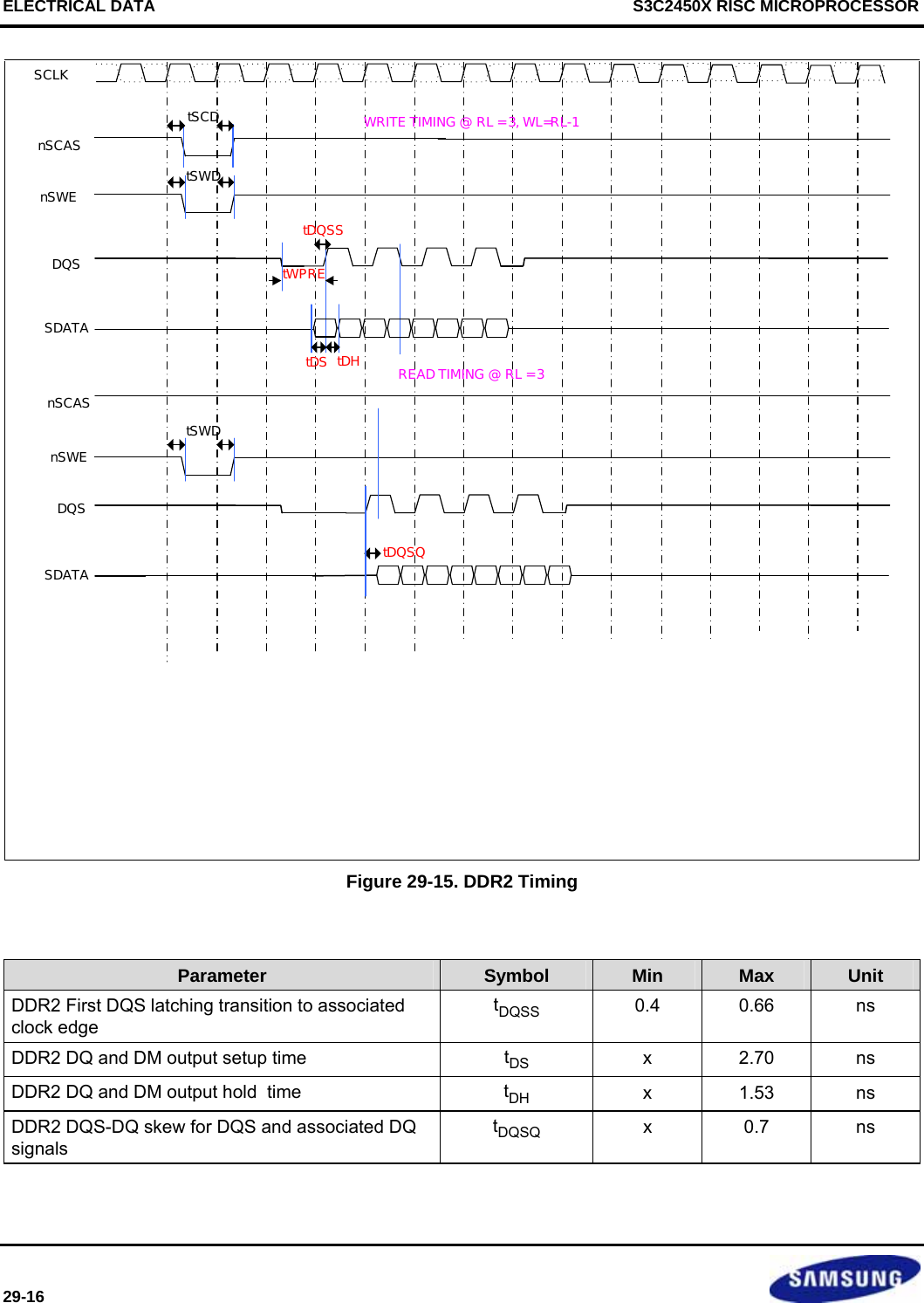
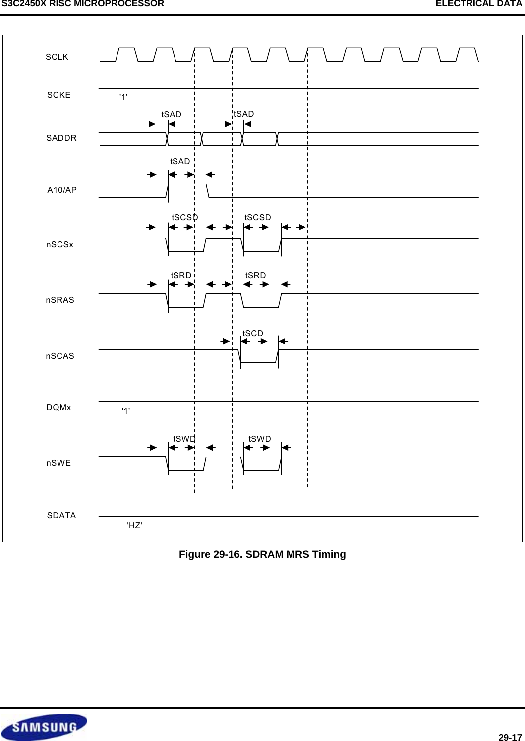
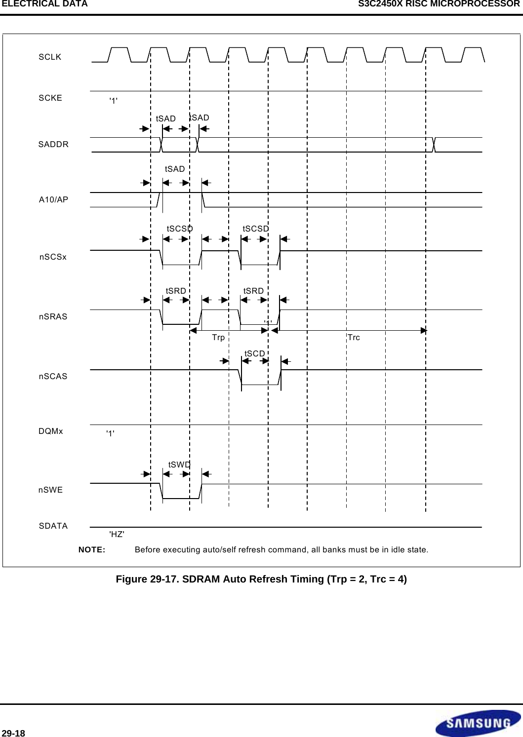
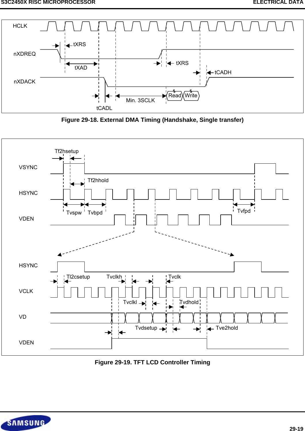
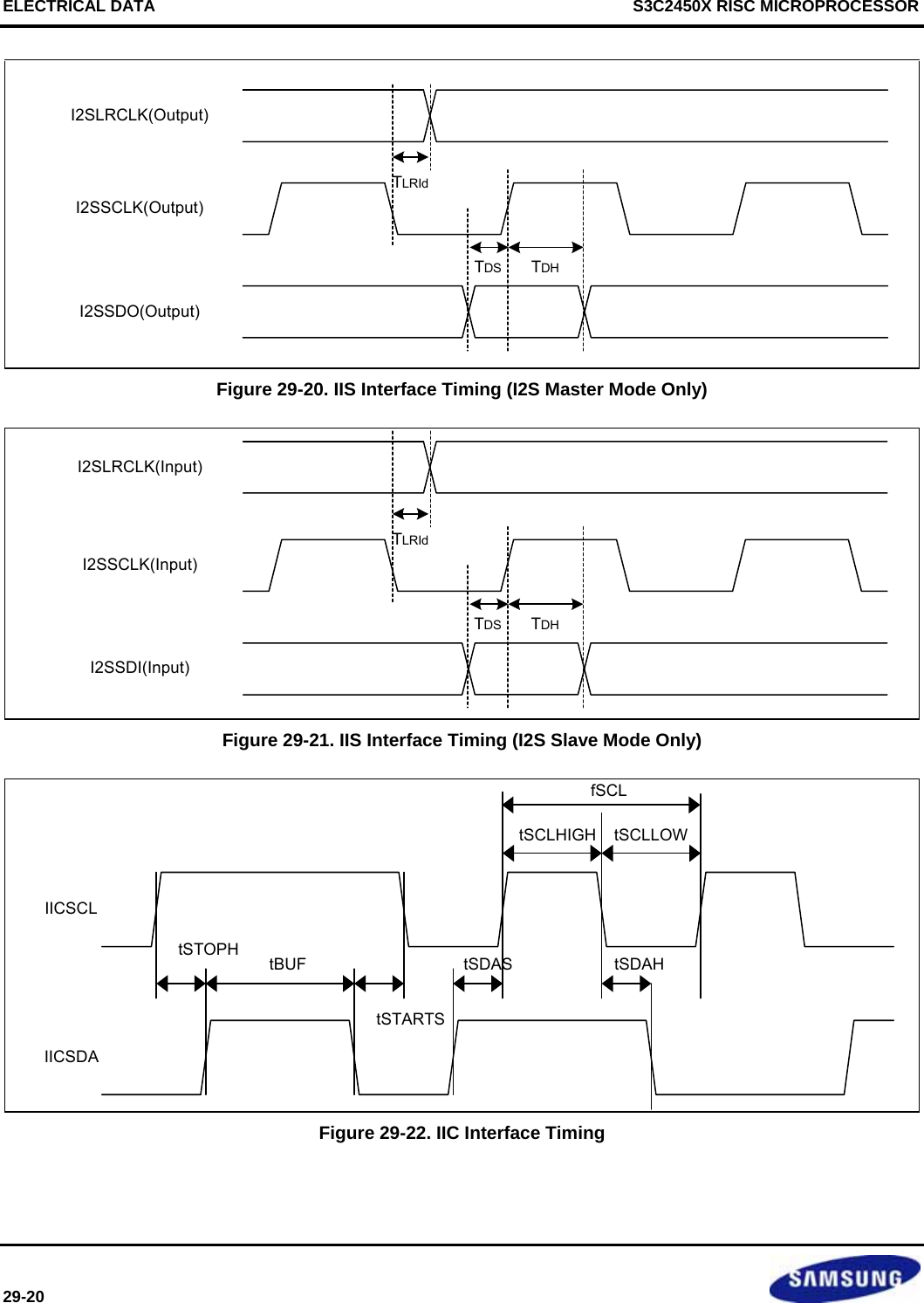
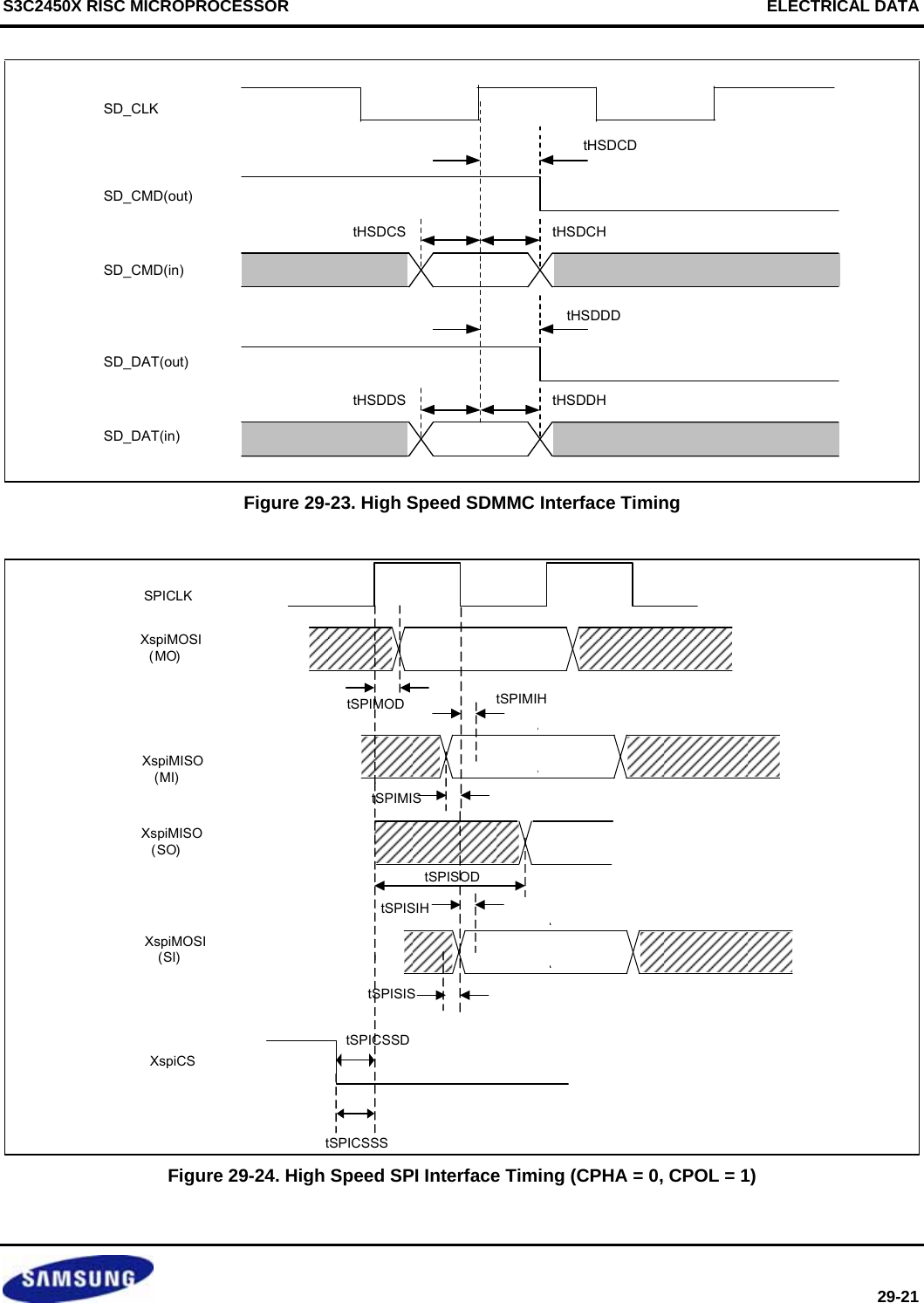
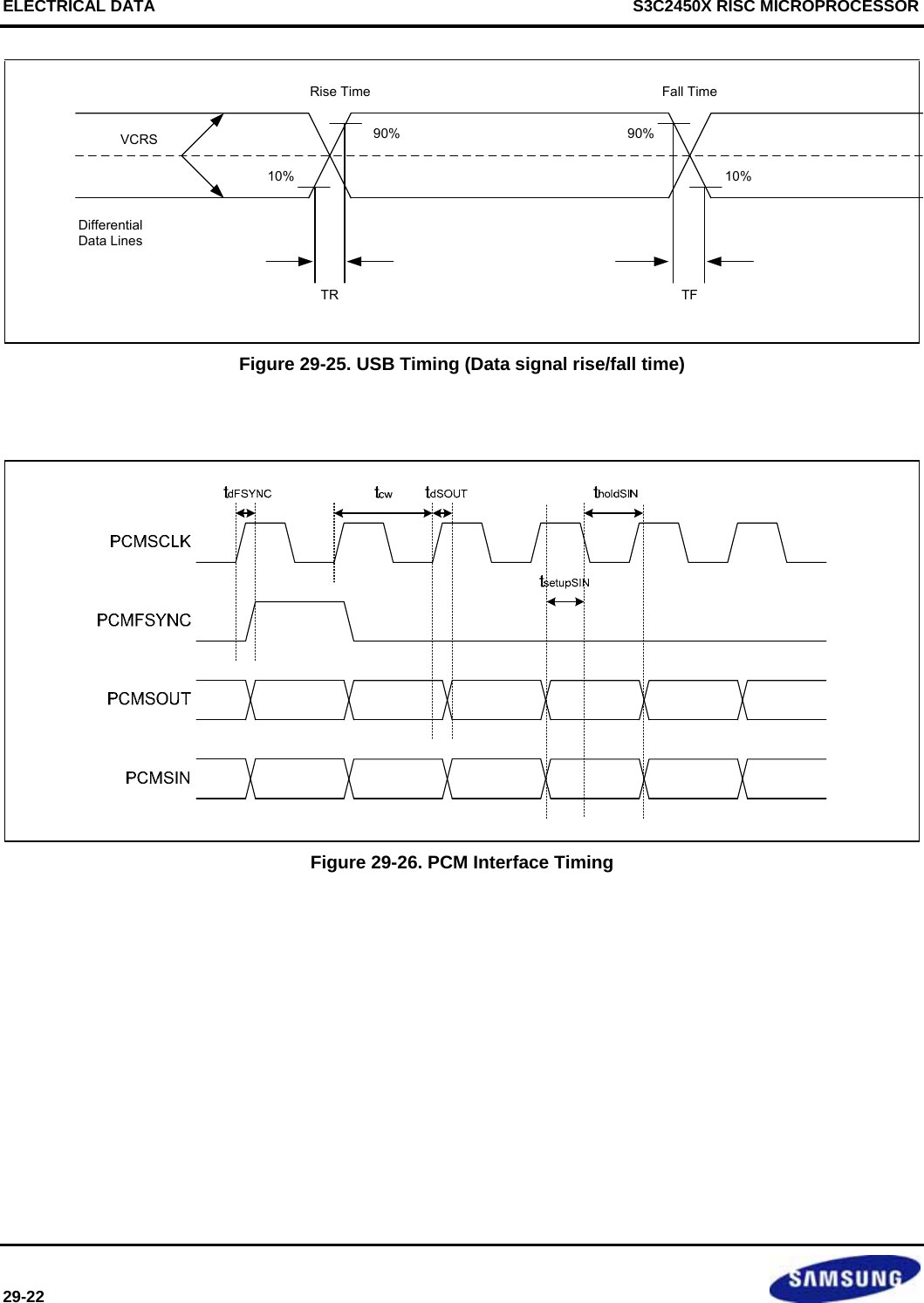
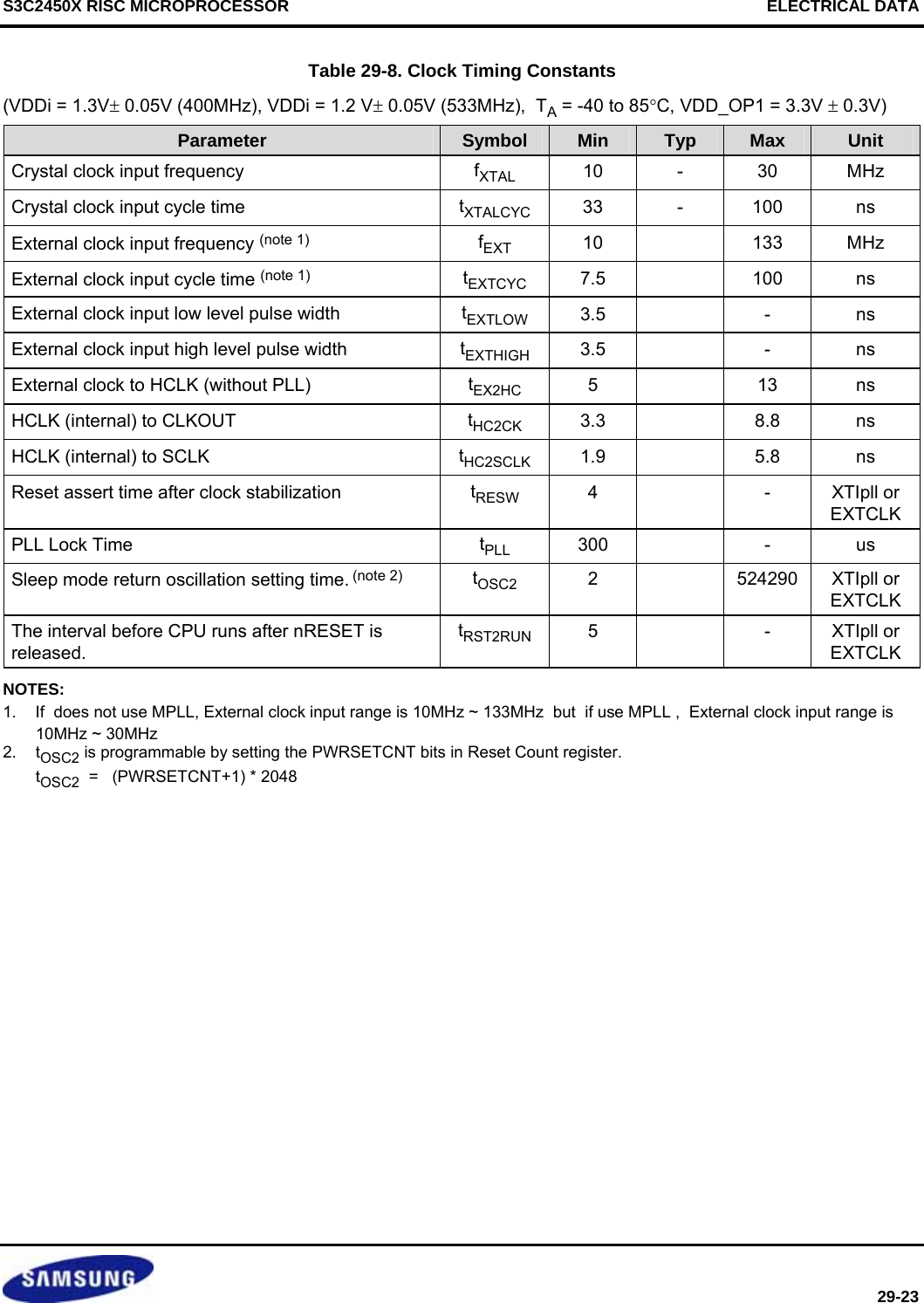
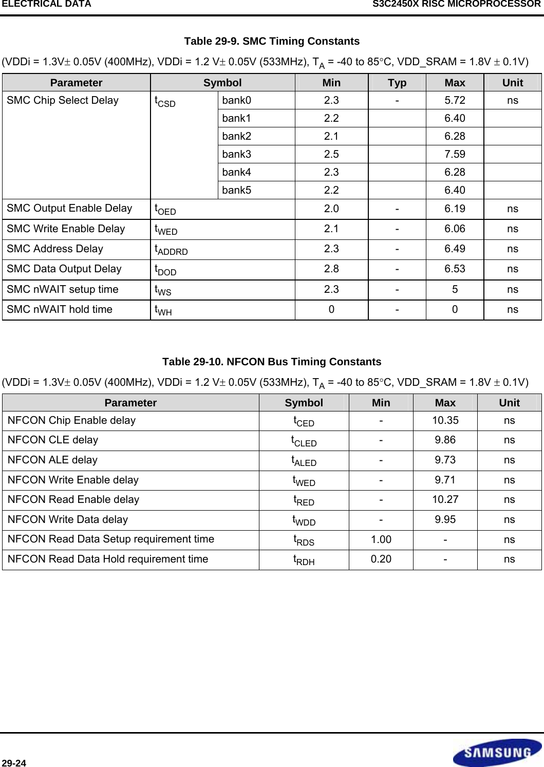
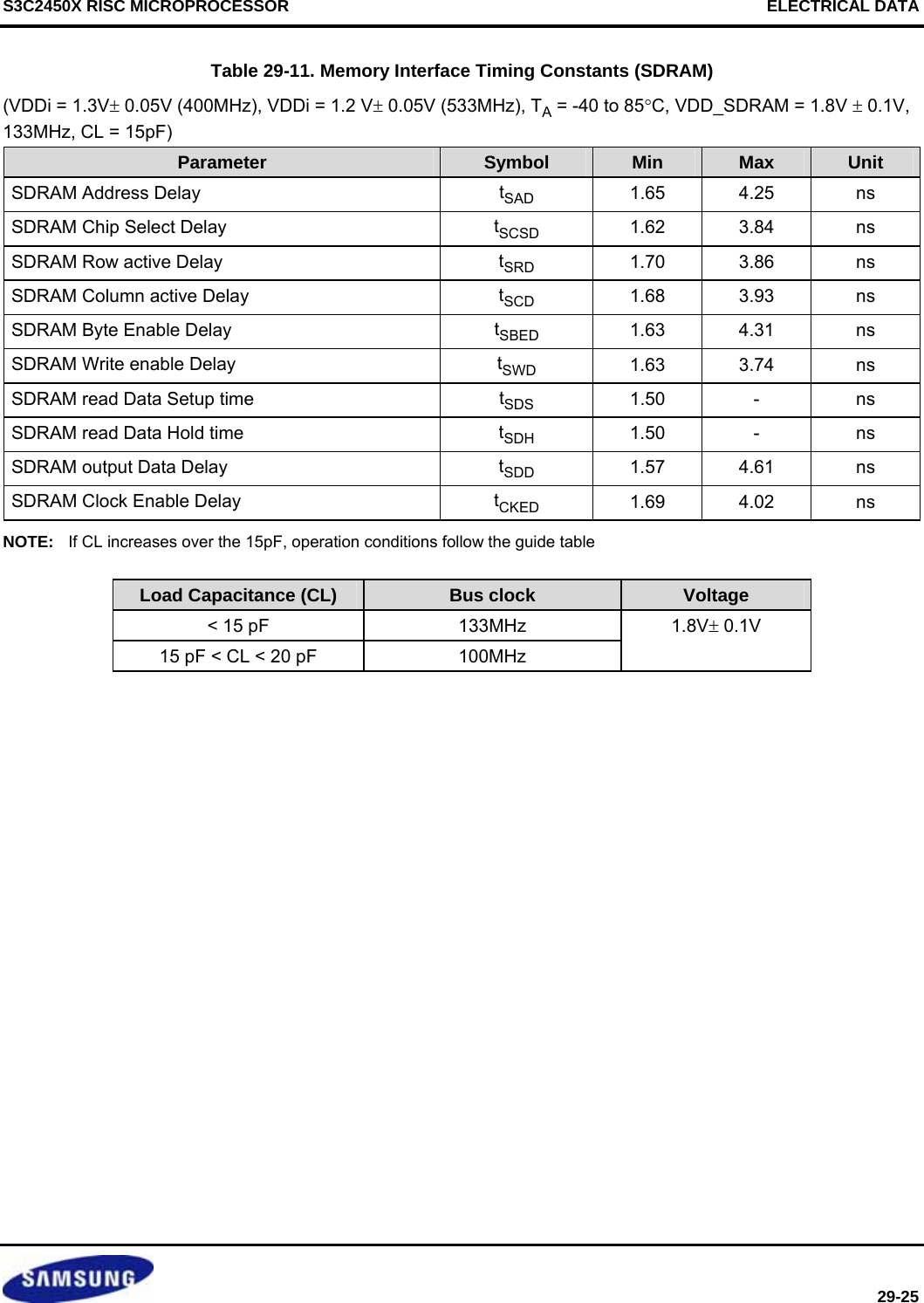
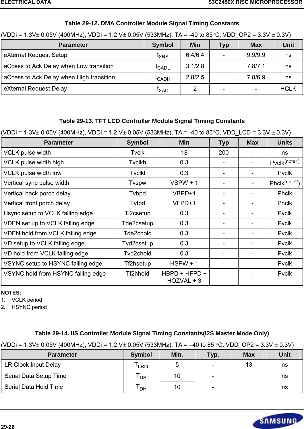
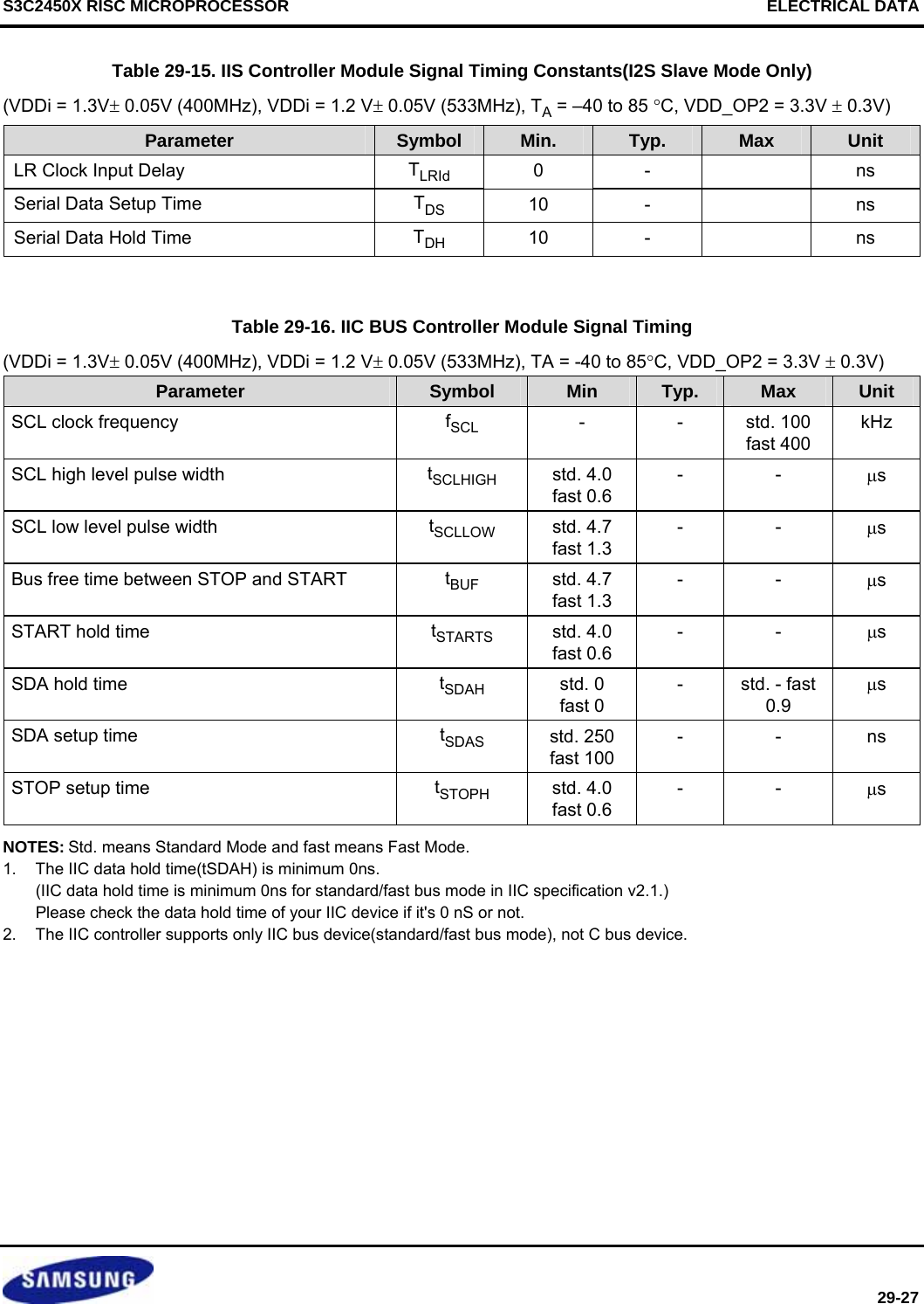
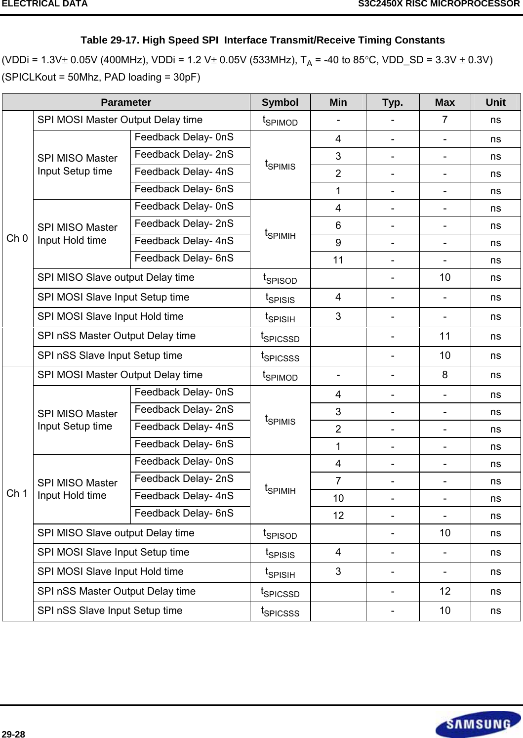
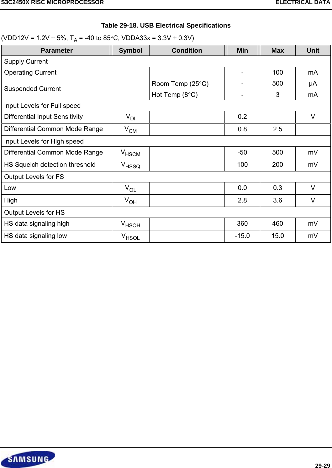
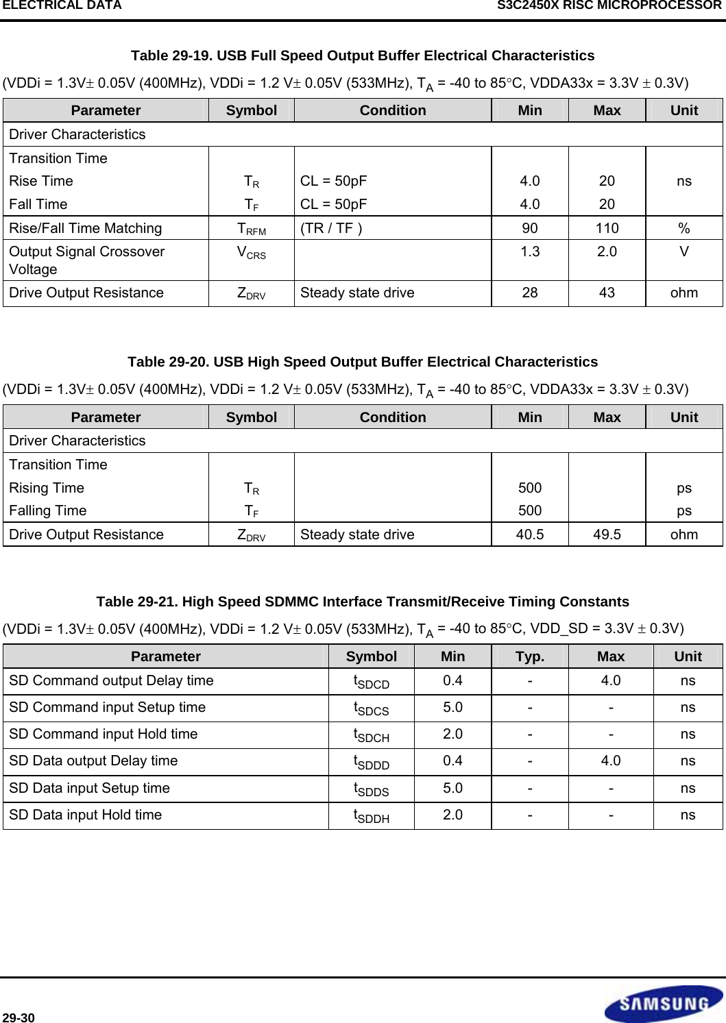
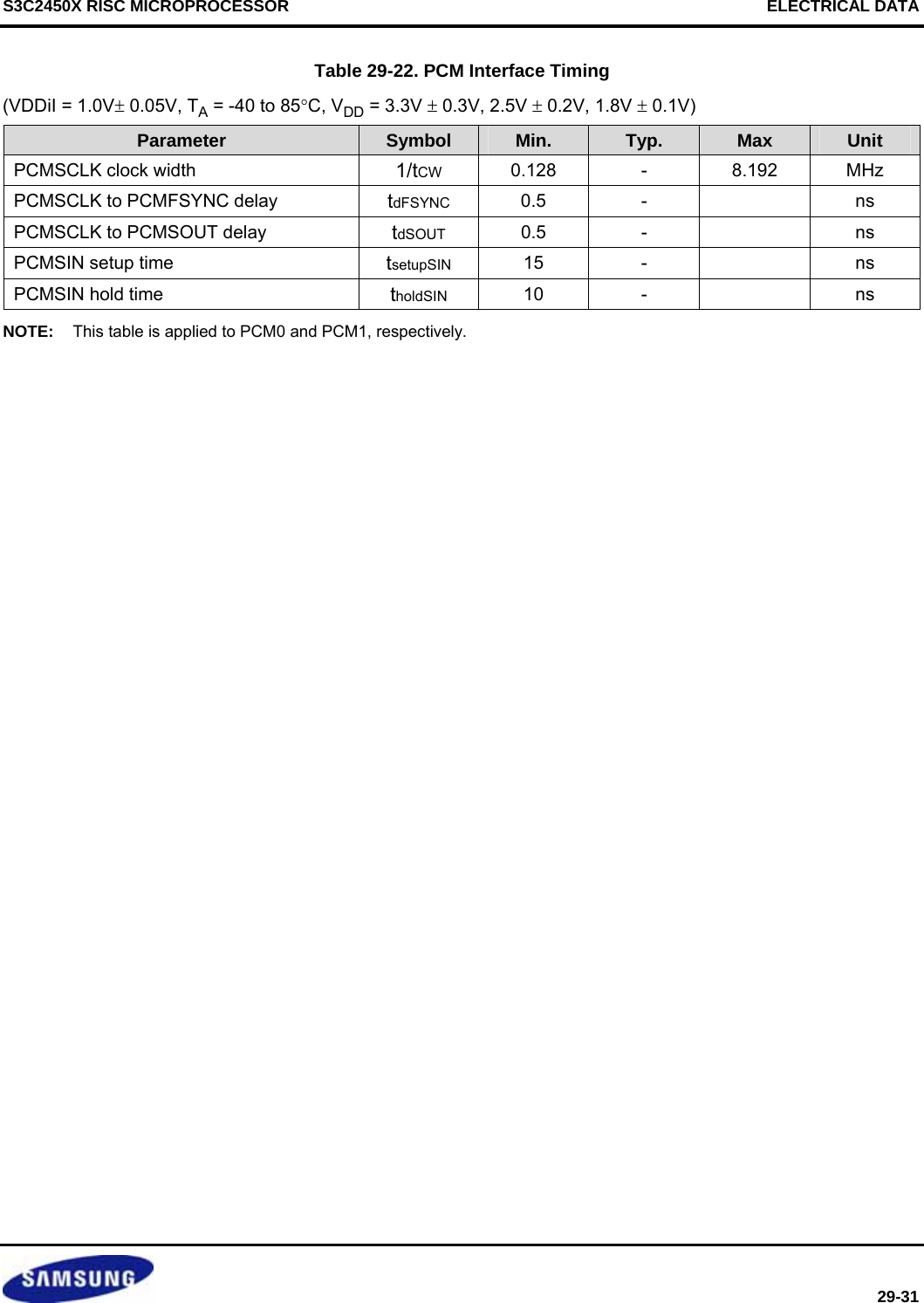

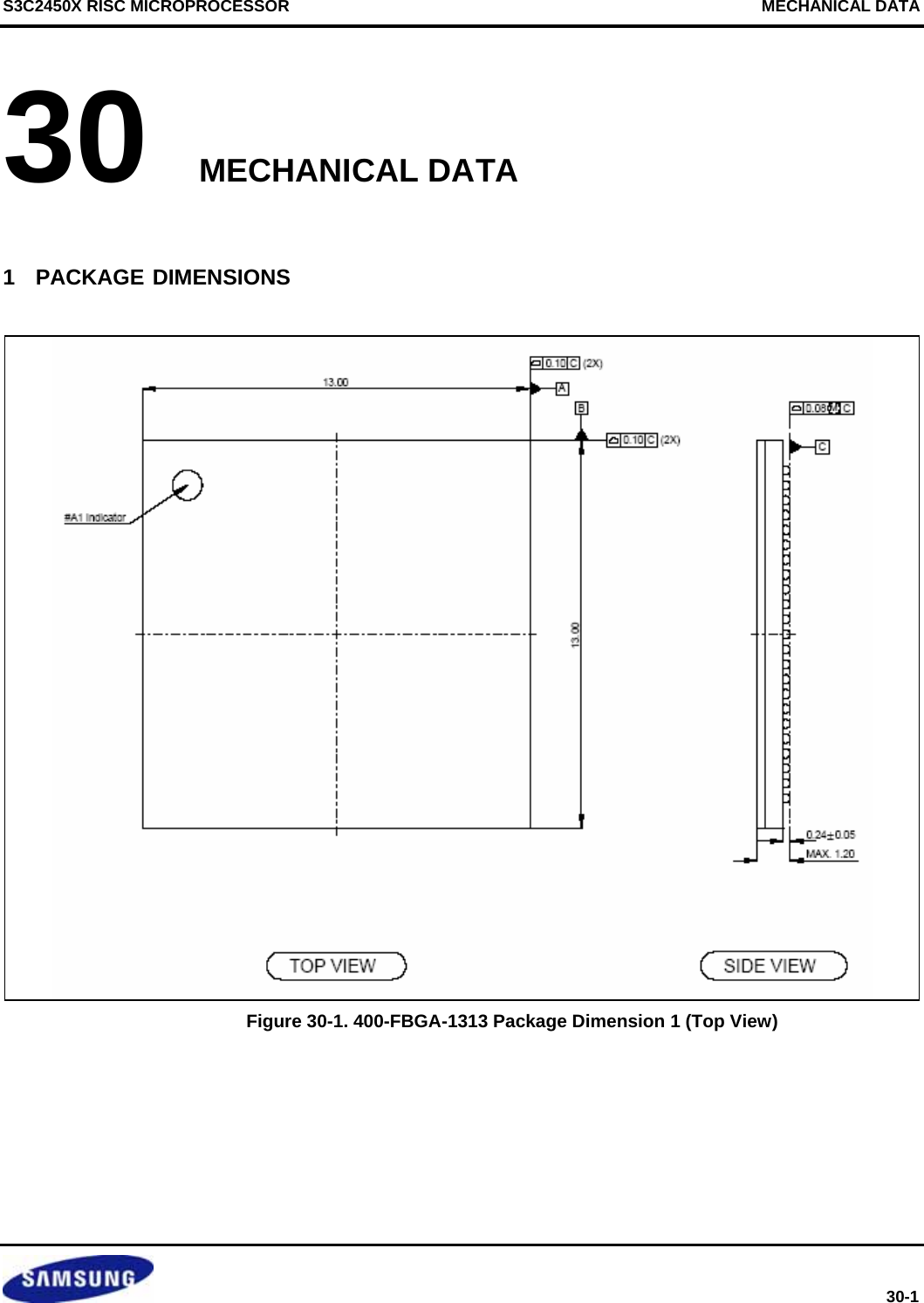
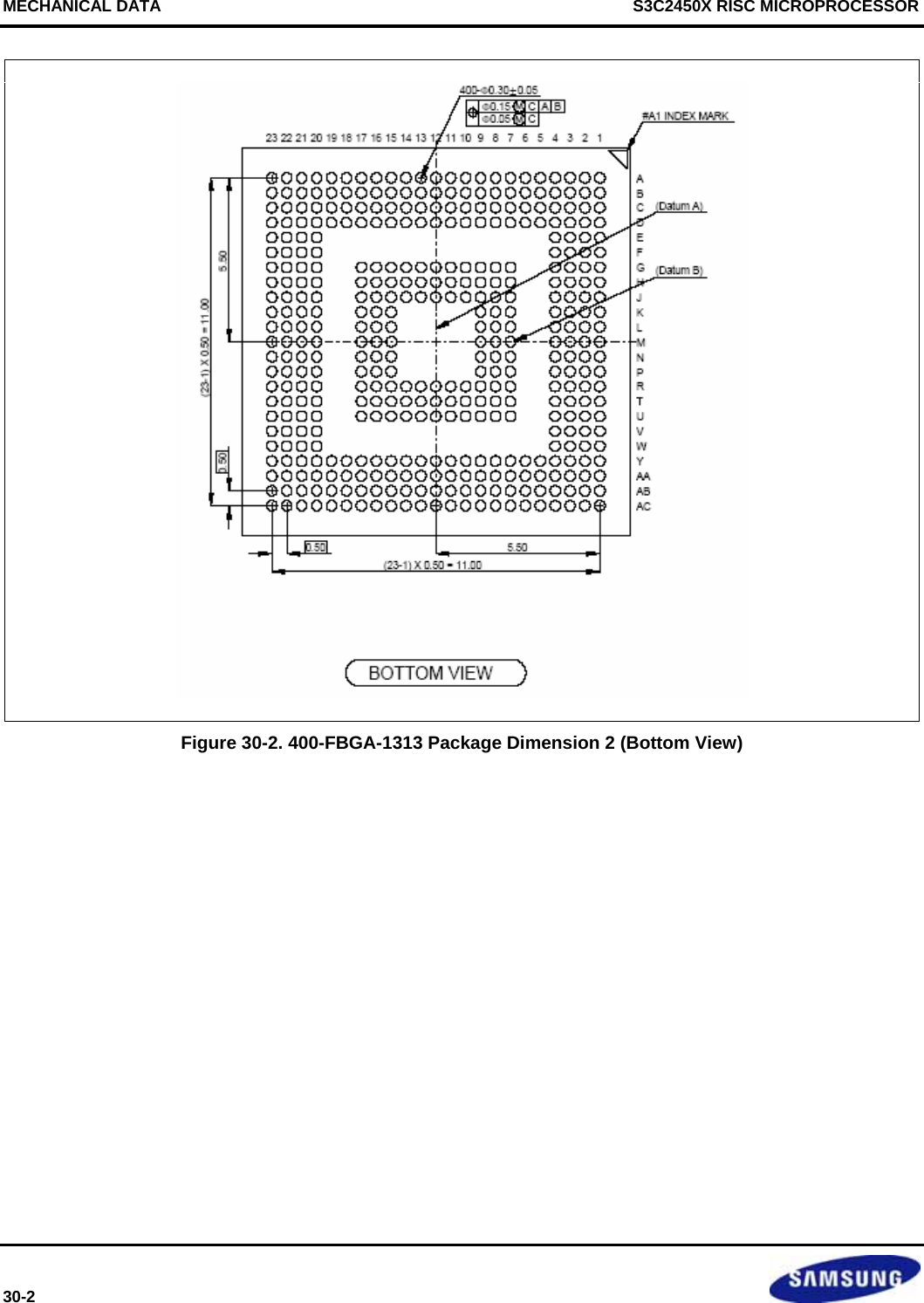
![SBM2XA-05 Data Sheet Copyright 2009 SungJin Techwin Co., Ltd.. 71.5 PIN Description Terminal No. Terminal Name Type Description (1) SPK_R- Analogue (output) Speaker output negative(right Channel) (2) SPK_R+ Analogue (output) Speaker output positive(right Channel) (3) AIO[0] Bi-directional Programmable input/output line (4) AIO[1] Bi-directional Programmable input/output line (5) VDD_USB VDD (Input) Positive supply for USB ports (3.3V) (6) USB_DN Bi-directional USB data minus (7) USB_DP Bi-directional USB data plus with selectable internal 1.5kΩ pull-up resistor (8) PIO[4] Bi-directional with programmable strength internal pull-up/down PIO or USB on (input senses when VBUS is high, wakes BlueCore3-Multimedia) (9) PIO[5] Bi-directional with programmable strength internal pull-up/down PIO line or chip detaches from USB when this input is high (10) PIO[6] Bi-directional with programmable strength internal pull-up/down PIO line or clock request output to enable external clock for external clock line (11) PIO[7] Bi-directional with programmable strength Programmable input/output line or programmable frequency clock output (12) GND GND GND (13) UART_TX CMOS output, tri-state, with weak internal pull-up UART data output (14) UART_RX CMOS input with weak internal pull-down UART data input (15) PCM_CLK Bi-directional with weak internal pull-down Synchronous data clock (16) PCM_IN CMOS input with weak internal pull-down Synchronous data input (17) MIC_L+ Analogue (Input) Microphone Right channel input positive (18) PCM_SYNC Bi-directional with weak internal pull-down Synchronous data sync (19) PCM_OUT CMOS output, tri-state, with weak internal pull-up Synchronous data output (20) MIC_L- Analogue (Input) Microphone Right channel input negative (21) MIC_R+ Analogue (Input) Microphone Left channel input positive (22) GND GND GND (23) MIC_R- Analogue (Input) Microphone Left channel input negative (24) SPI_MISO CMOS input with weak internal pull-down Serial Peripheral Interface data output (25) SPI_MOSI CMOS input with weak internal pull-down Serial Peripheral Interface data input (26) SPI_CSB CMOS input with weak internal pull-up Chip select for Synchronous Serial Interface, active low (27) SPI_CLK CMOS input with weak internal pull-down Serial Peripheral Interface clock](https://usermanual.wiki/Diasonic-Technology-Co/RVM-704M.Users-Manual/User-Guide-1826140-Page-801.png)
![SBM2XA-05 Data Sheet Copyright 2009 SungJin Techwin Co., Ltd.. 8 (28) IMIC BIAS Analogue Microphone bias (29) PIO[11] Bi-directional with programmable strength internal pull-up/down Programmable input/output line (30) PIO[10] Bi-directional with programmable strength internal pull-up/down Programmable input/output line (31) PIO[9] Bi-directional with programmable strength internal pull-up/down Programmable input/output line (32) PIO[8] Bi-directional with programmable strength internal pull-up/down Programmable input/output line (33) ANT For Antenna /50ohm (34) GND GND (35) PIO[3] Bi-directional with programmable strength internal pull-up/down PIO or output goes high to wake up PC when in USB mode or clock request input from host controller (36) PIO[2] Bi-directional with programmable strength internal pull-up/down PIO or external clock request (37) PIO[1] Bi-directional with programmable strength internal pull-up/down Control output for external PA(if fitted) (38) PIO[0] Bi-directional with programmable strength internal pull-up/down Control output for external TX/RX(if fitted) (39) VDD_1V8 1.8V Out For Test (40) RESET RESET (Active: Low) (41) VDD VDD 2.7V ~ 3.7V Voltage input (42) SPK_L- Analogue (output) Speaker output negative(left Channel) (43) SPK_L+ Analogue (output) Speaker output positive(left Channel)](https://usermanual.wiki/Diasonic-Technology-Co/RVM-704M.Users-Manual/User-Guide-1826140-Page-802.png)
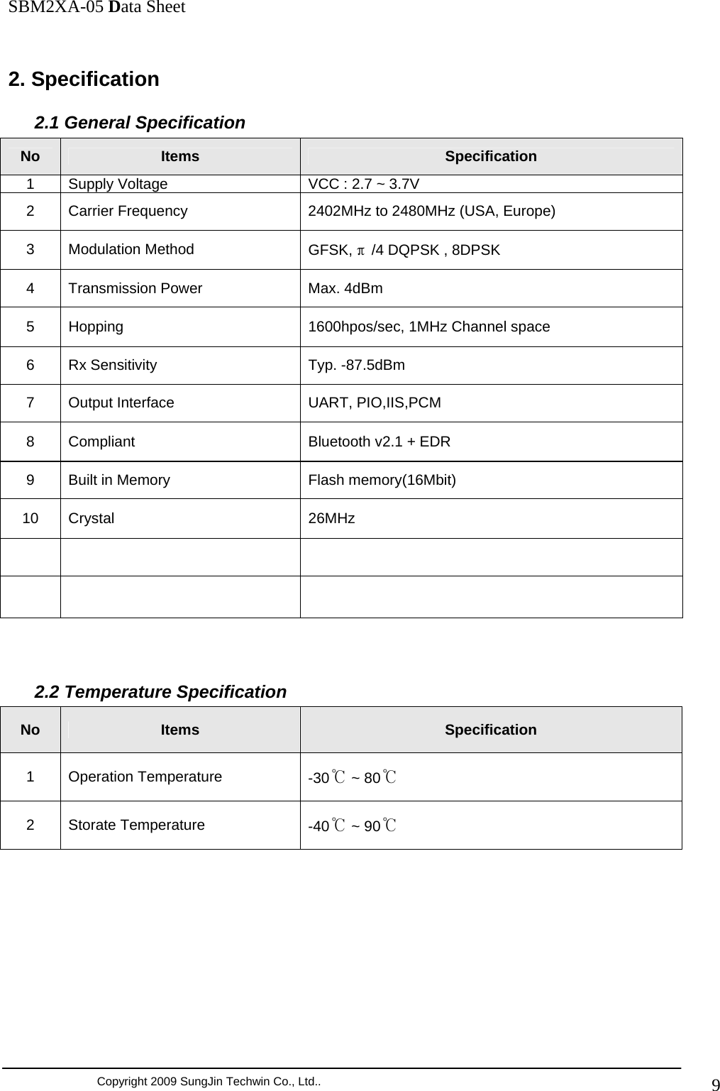
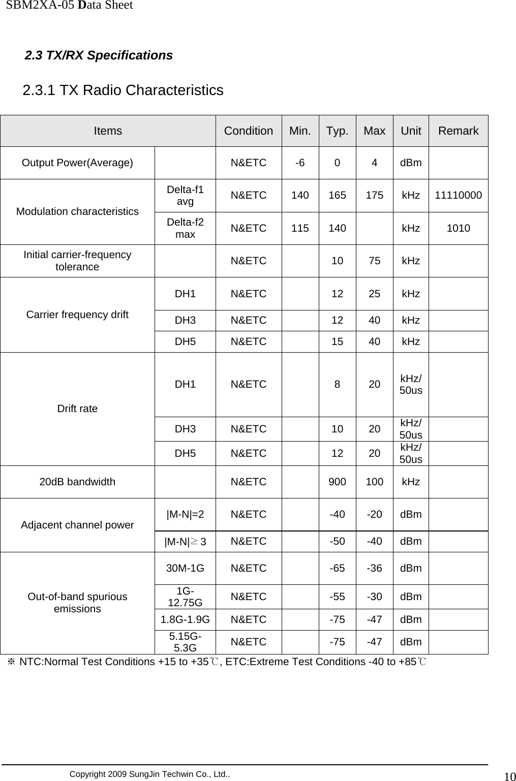
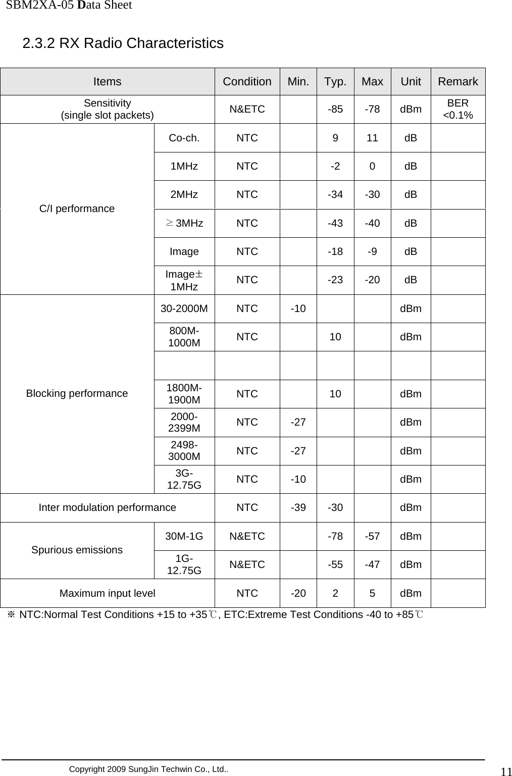
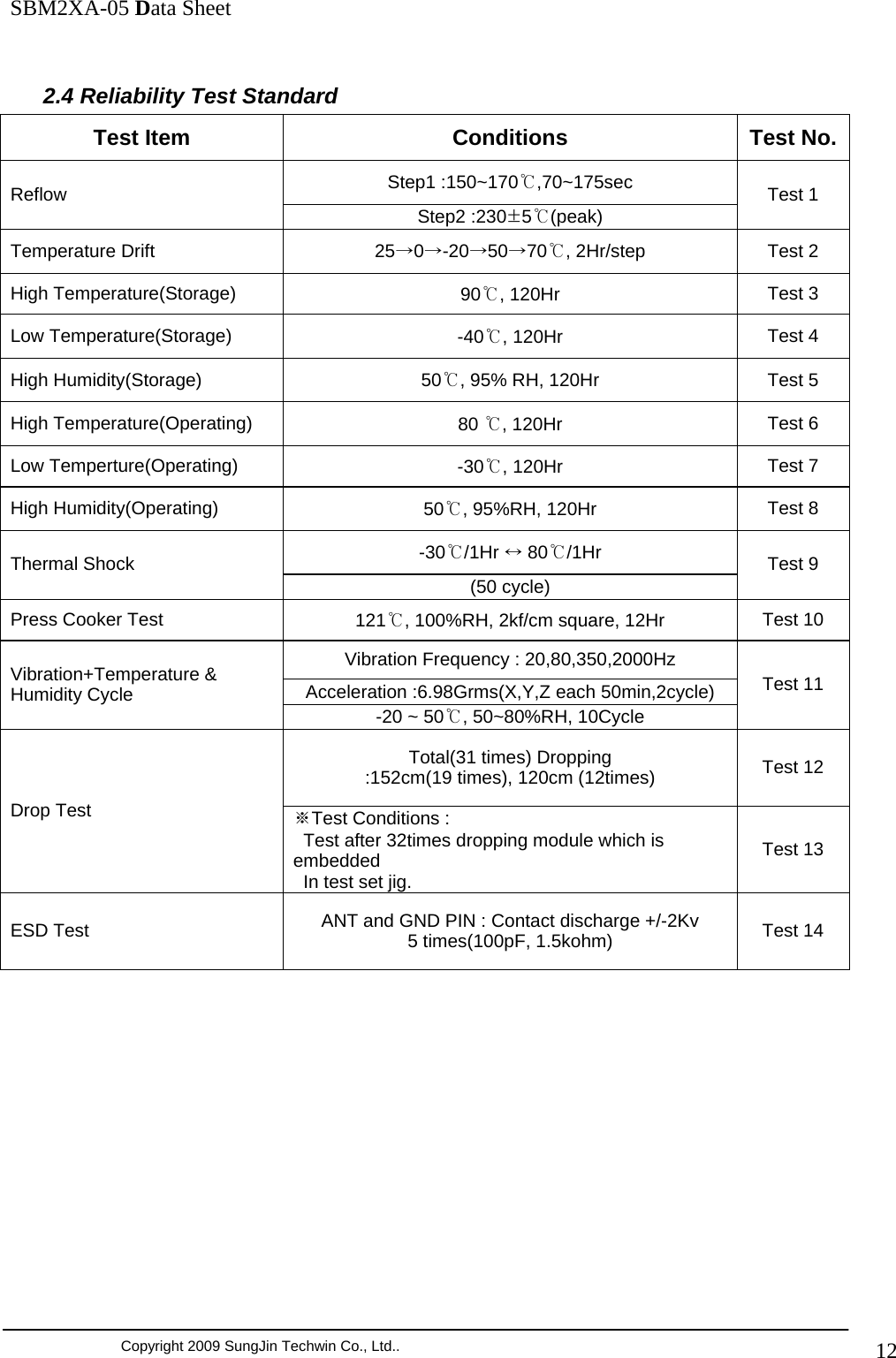
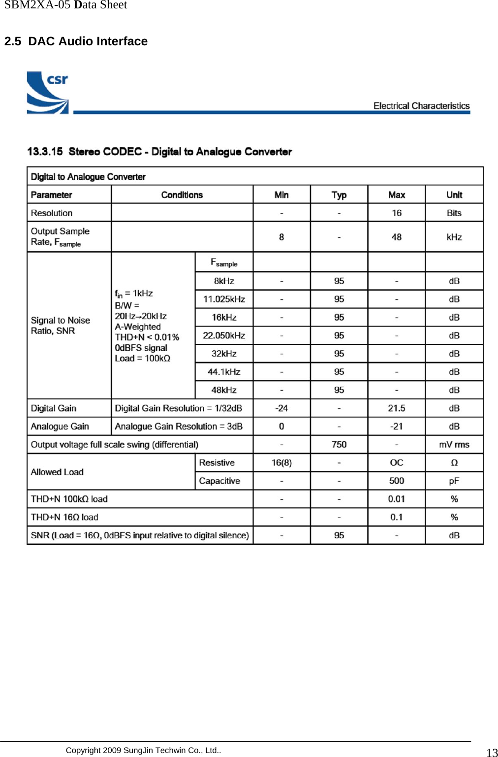
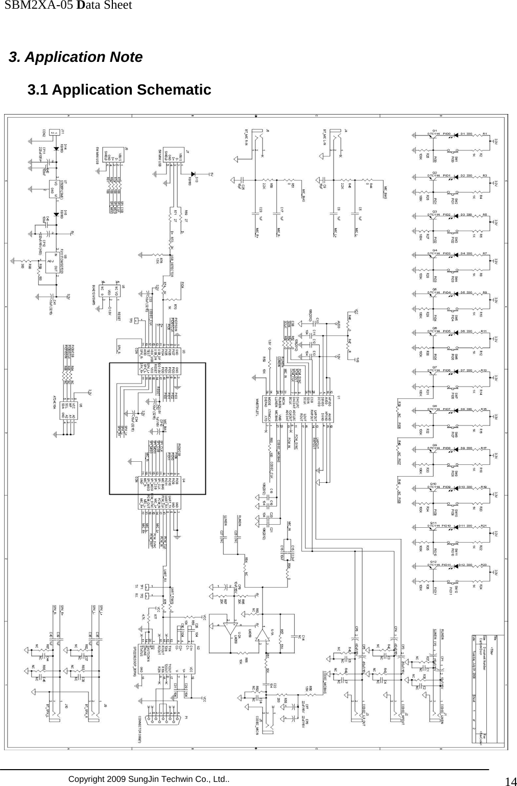
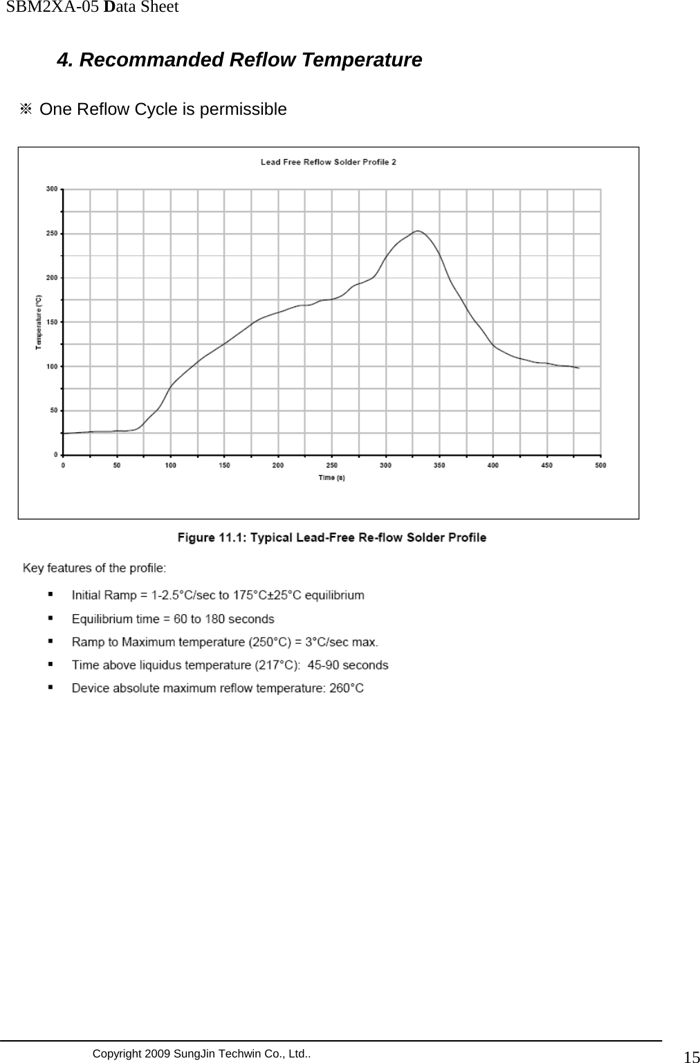
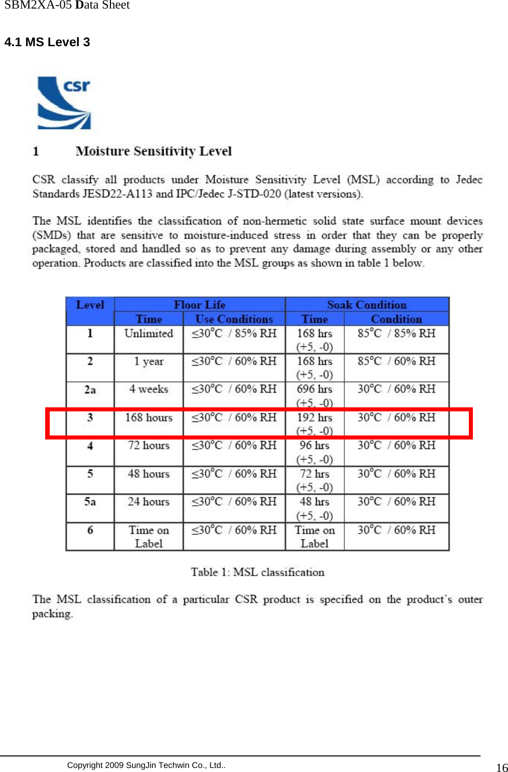
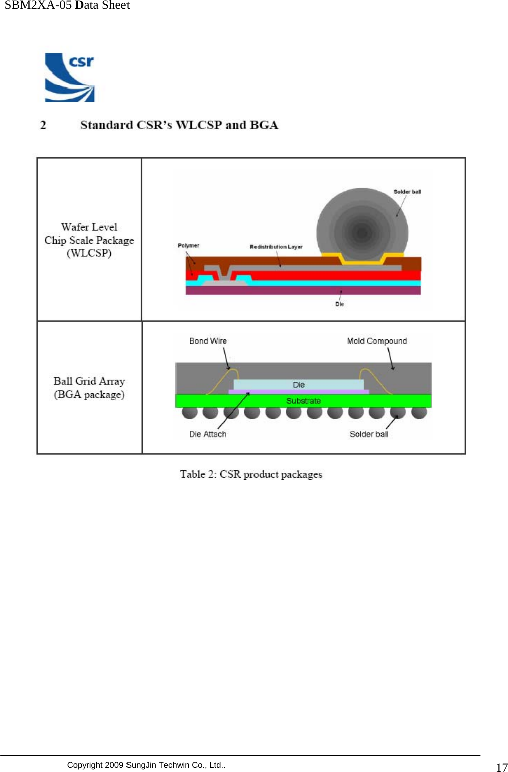
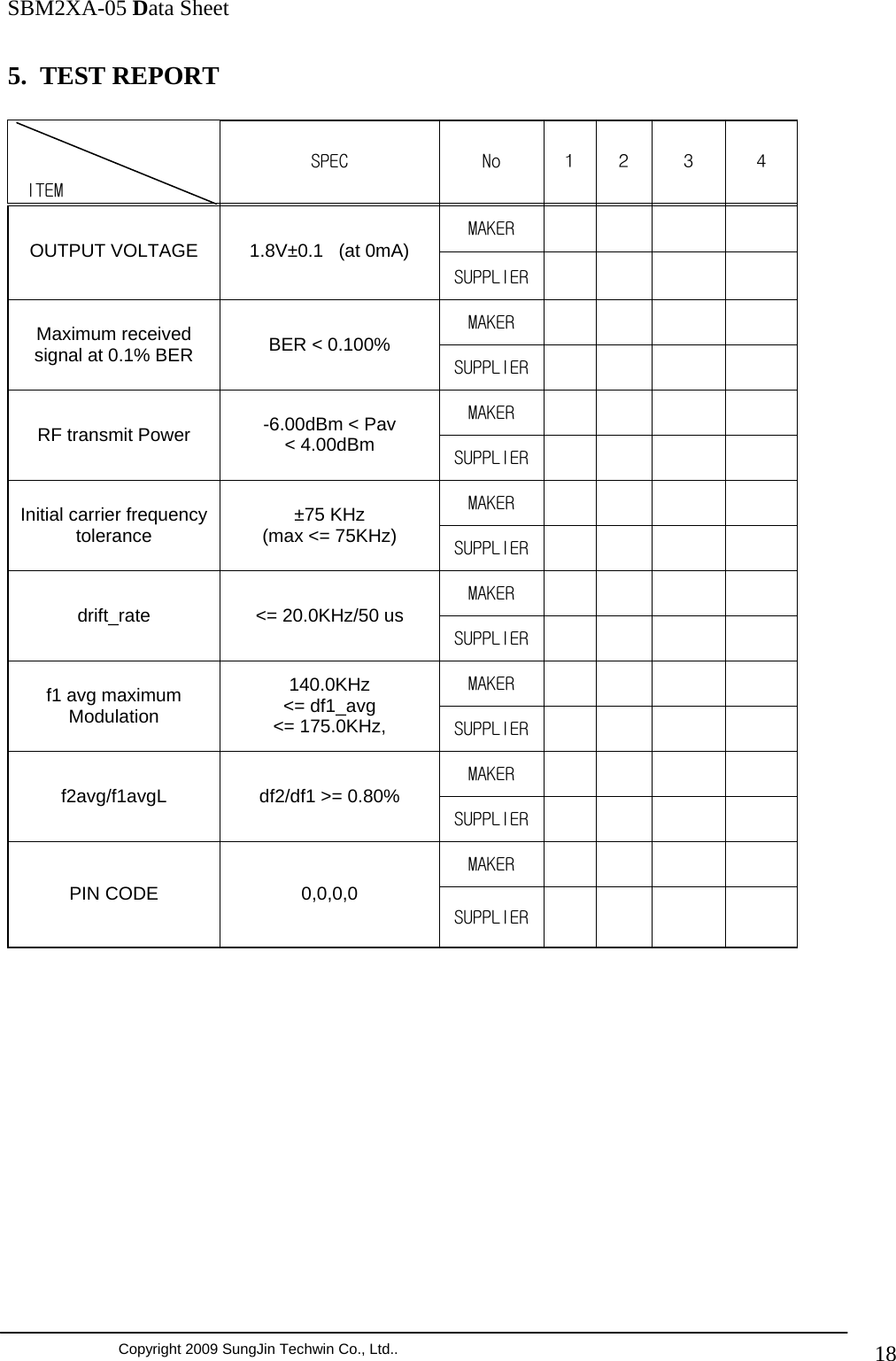
![SBM2XA-05 Data Sheet Copyright 2009 SungJin Techwin Co., Ltd.. 196. Test Procedure 6.1. OUTPUT VOLTAGE 1.8V±0.1 (at 0mA) 6.2. Maximum received signal at 0.1% BER(bit error rate) : BER < 0.100% 6.3. RF transmit Power : -6.00dBm < Pav < 4.00dBm 6.4. Modulation Characteristics : ±75 KHz (max <= 75KHz) : 6.5. Initial Carrier Frequency Tolerance (drift_rate) : <= 20.0KHz/50 us 6.6. CarrierFrequency Drift (f1 avg maximum Modulation) : 140.0KHz <= df1_avg <= 175.0KHz, 6.7. "CarrierFrequency Drift (f2avg/f1avgL) : df2/df1 >= 0.80% 6.8. PIN CODE : [0,0,0,0] : Security](https://usermanual.wiki/Diasonic-Technology-Co/RVM-704M.Users-Manual/User-Guide-1826140-Page-813.png)