Digi 50M1355 Communication Bridge User Manual ConnectCore 9C Wi 9C Hardware Reference
Digi International Inc Communication Bridge ConnectCore 9C Wi 9C Hardware Reference
UserManual.wiki
>
Digi
>
50M1355 User Manual
Users Manual
Navigation menu
Upload a User Manual
Namespaces
Wiki Guide
HTML
PDF
Info
Views
User Manual
Discussion / Help
Navigation
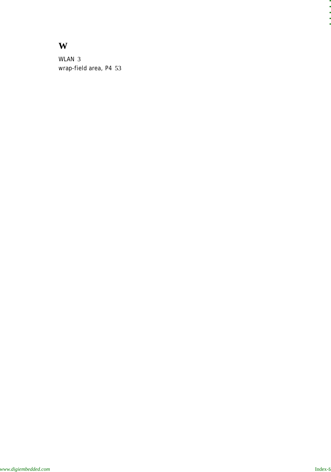
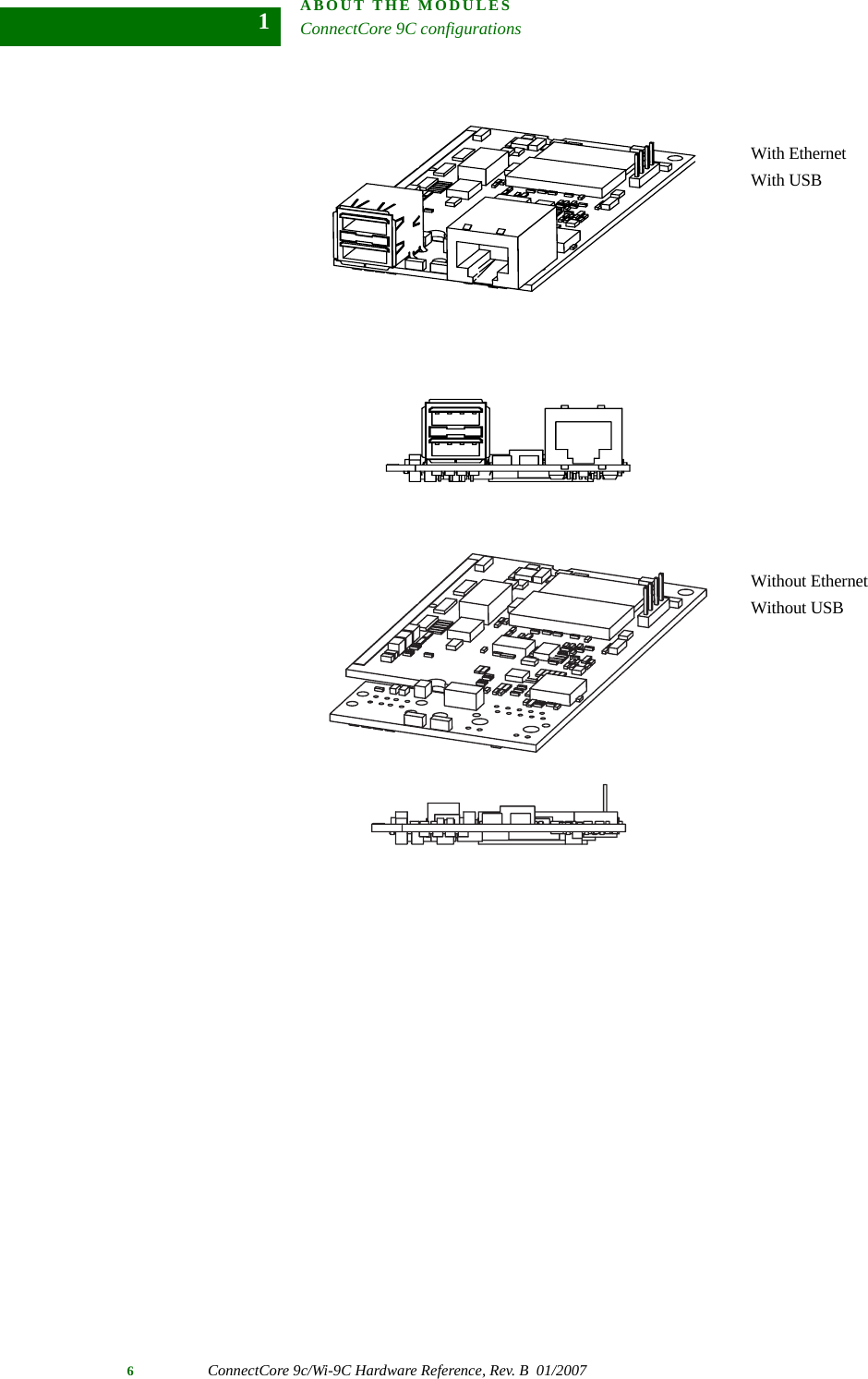
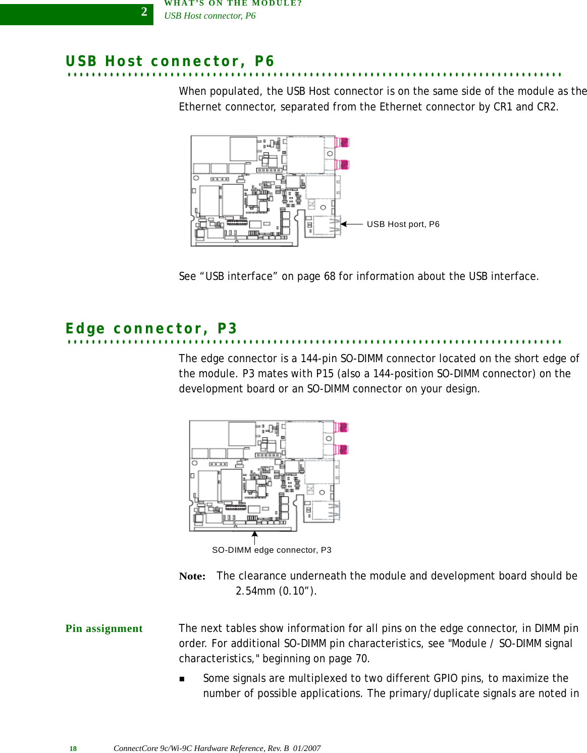
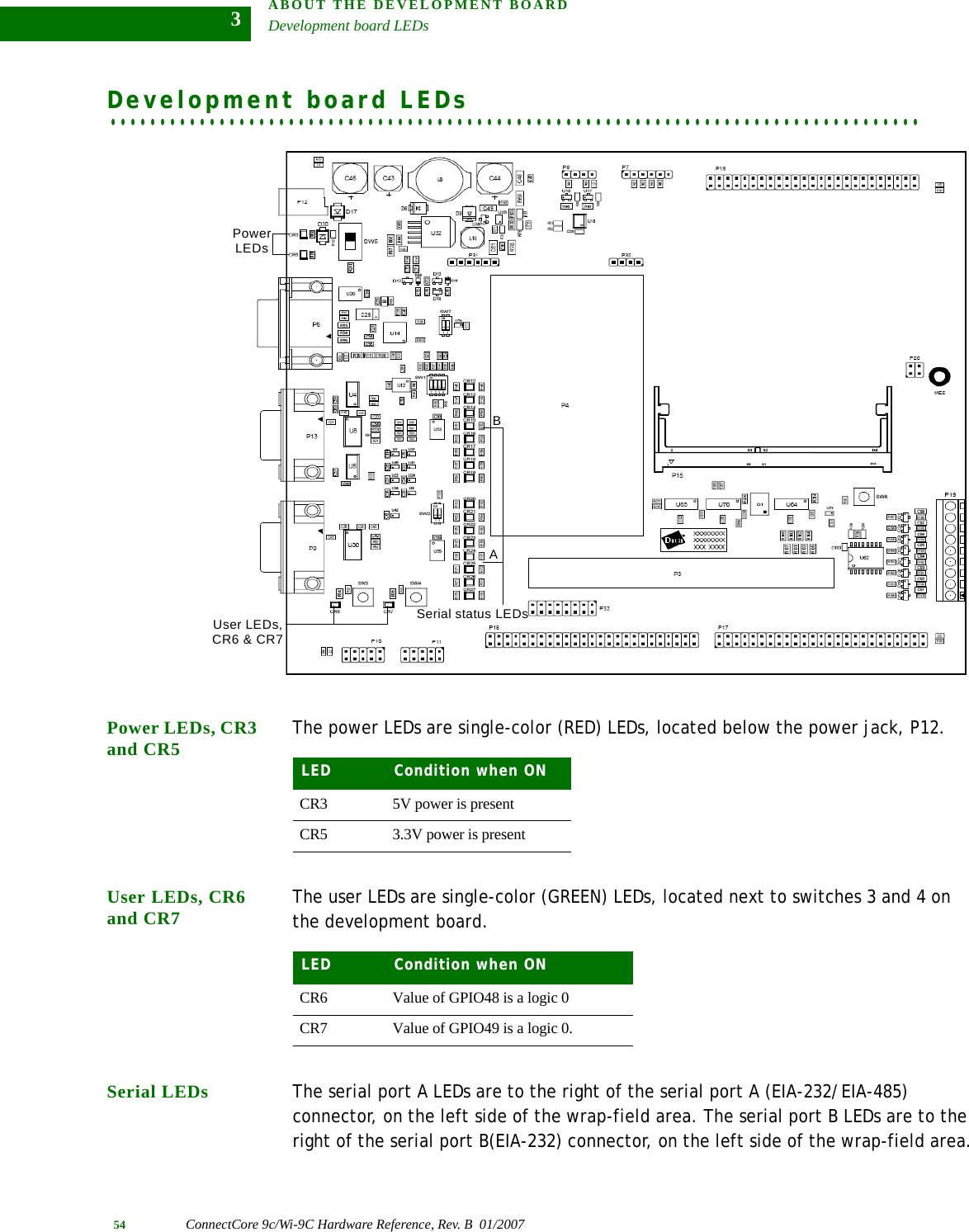
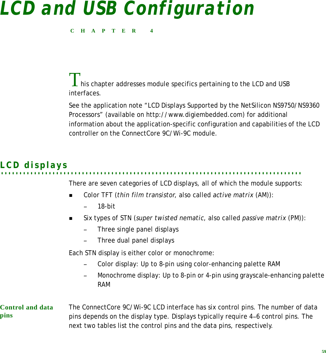
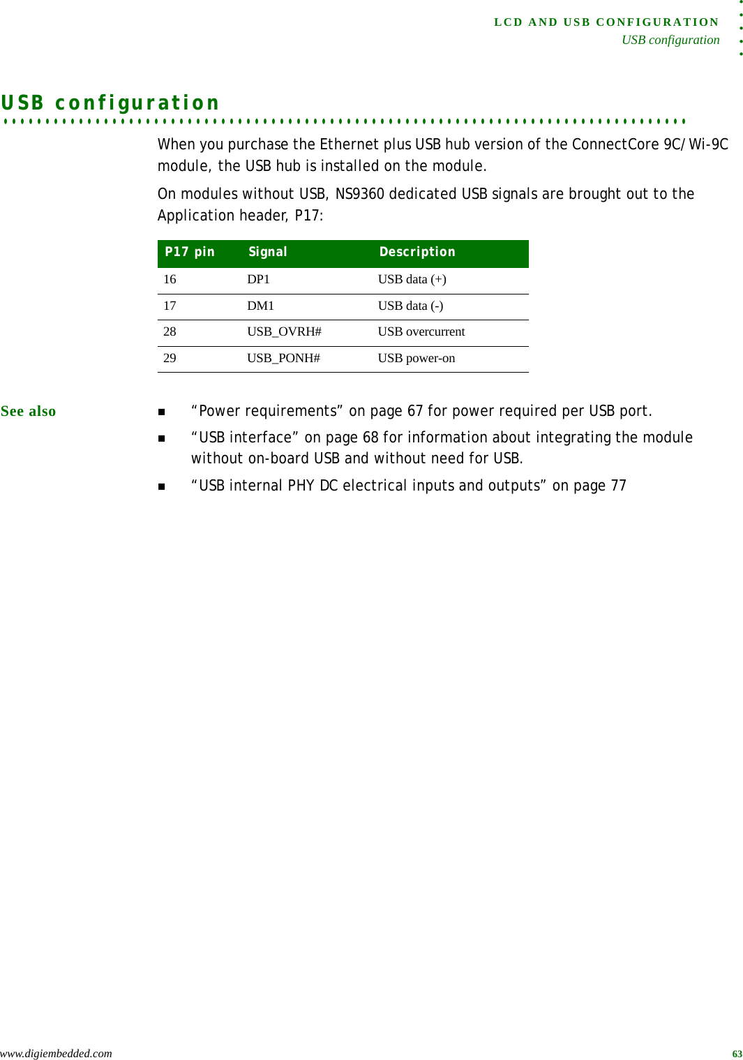
![ABOUT THE MODULESInterfaces2ConnectCore 9c/Wi-9C Hardware Reference, Rev. B 01/20071Integrated LCD controllerUp to eight independent 16-/32-bit programmable timers, counters, or four PWM functionsFour programmable external interruptsUp to 55 shared General Purpose Input/Output (GPIO) ports–Up to seven high-current (8mA) pins8-bit wide data/address bus with external chip selectProcessor-powered on-chip Real-Time Clock (RTC)Population options available (processor speed, memory, connectors)Wi-9C specific features802.11b/g WLAN interfaceWEP, WPA, and WPA2/802.11i security standardSingle or dual-diversity antenna optionsMemory The module’s standard memory configuration is 4 MB Flash and 16 MB SDRAM.Memory clocks Memory clocks = 77.5 MHzNot available for off-DIMM useclk_out[0] — Not used; turned off by codeclk_out[1] — Connected to clk_inclk_out[2] — Used for one bank of two X16 SDRAMSclk_out[3] — Not usedOther system clocksSource clock is a 29.4912 MHz crystal or spread spectrum oscillator.USB uses a 48.000 MHz oscillatorEthernet versions have a 25.0000 MHz crystal. . . . . . . . . . . . . . . . . . . . . . . . . . . . . . . . . . . . . . . . . . . . . . . . . . . . . . . . . . . . . . . . . . . . . . . . . . . . . . . . . .InterfacesThe ConnectCore 9C/Wi-9C module supports several system interfaces. This section details the features of these interfaces.Ethernet The module provides a 10/100 Mbps Ethernet interface with optional on-board RJ-45 connector and integrated LEDs. On modules not populated with the RJ-45 connector, the Ethernet PHY signals are available on the SO-DIMM edge connector.](https://usermanual.wiki/Digi/50M1355/User-Guide-781539-Page-12.png)


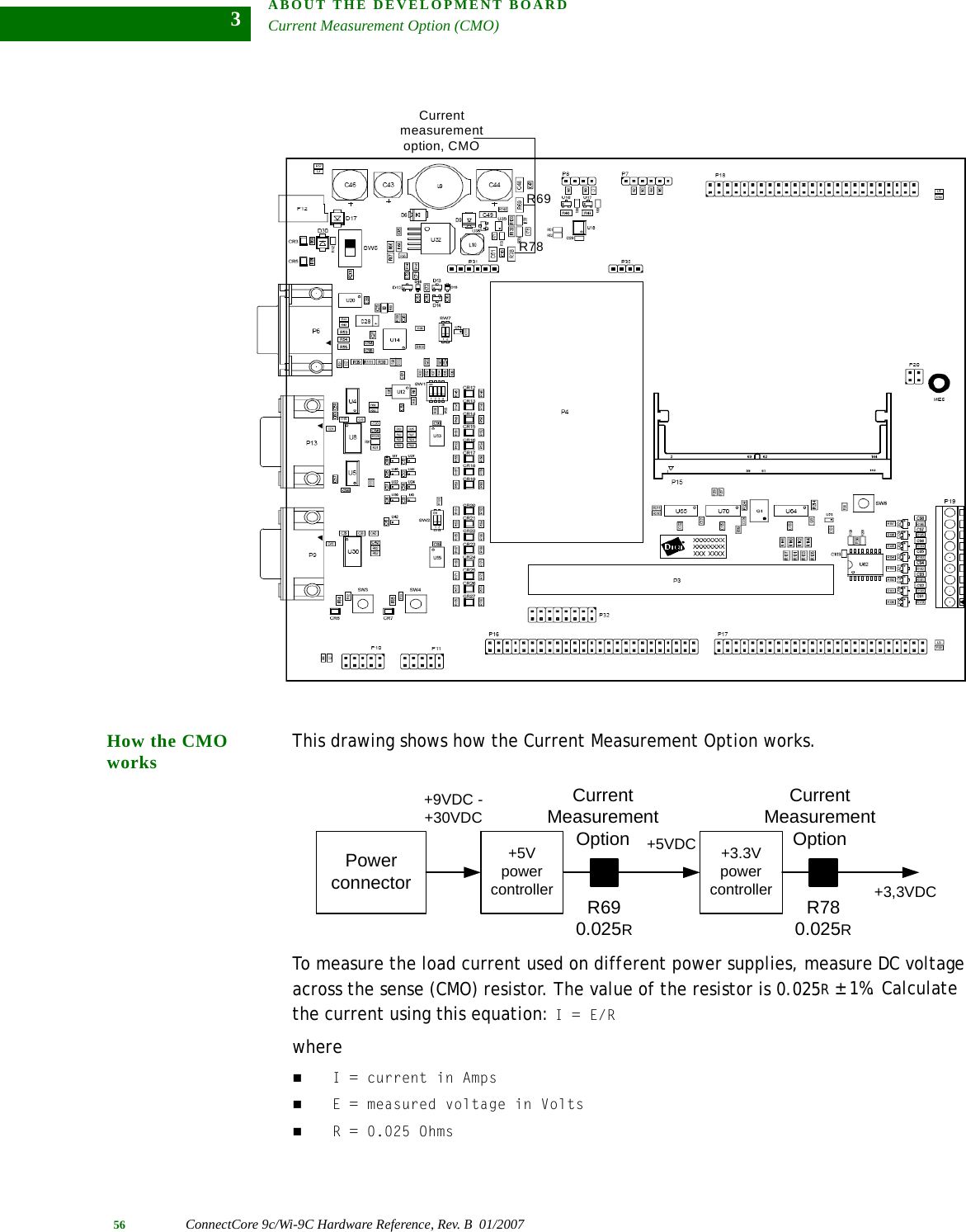
![WHAT’S ON THE MODULE?Edge connector, P320 ConnectCore 9c/Wi-9C Hardware Reference, Rev. B 01/2007219 GND Common GND return20 GND Common GND return21 ADDRESS_2 Address bus Wi-9C onlyCC9C: Reserved22 MFGI_GPIO[72] Reserved23 ADDRESS_3 Address bus Wi-9C onlyCC9C: Reserved24 GPIO[71] iic_sda GPIO[71]: Output drive 8mAiic_sda: Primary on GPIO[35]25 ADDRESS_4 Address bus Wi-9C onlyCC9C: Reserved26 GPIO[70] iic_scl GPIO[70]: Output drive 8mAiic_scl: Primary on GPIO[34]27 ADDRESS_5 Address bus Wi-9C onlyCC9C: Reserved28 GPIO[69] IRQ1 GPIO[69]: Output drive 8mAIRQ1: Primary on GPIO[07]Add 10-15K pullup if not used29 GND Common GND return30 GND Common GND return31 GPIO[27] DCD_D ENBL_D CLD3 TIMER432 No connect33 GPIO[26] RI_D CLK_D CLD2 TIMER334 GPIO[67] CR1: Green user LEDOutput drive 8mAMFGO_CR135 GPIO[25] DSR_D CLD136 GPIO[66] CR2: Yellow user LEDOutput drive 8mA37 GPIO[24] BS:CS1_MSB DTR_D CLD038 GPIO[23] DCD_C ENBL_C CLLE39 GND Common GND return40 GND Common GND return41 GPIO[47] CTS_D RXD- PINIT# RXD-: Only used for unidirectional PHY42 GPIO[22] RI_C CLK_C CLAC43 GPIO[46] RTS_D RXD+ PAFD# RXD+: Only used for unidirectional PHY44 GPIO[21] DSR_C CLFP VSYNC45 GPIO[45] RXD_D DIN_D RCV PSTB#Dimm Pin Signal BootStrap (BS) / System / Other UART SPI I2C USB LCD IEEE 1284 PWM / Timer / IRQNotes](https://usermanual.wiki/Digi/50M1355/User-Guide-781539-Page-30.png)
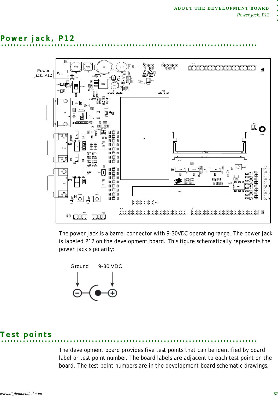
![. . . . .WHAT’S ON THE MODULE?Edge connector, P3www.digiembedded.com 2146 GPIO[20] BS: CS1_LSB DTR_C CLCP/LDCCLKO GPIO[20]: Output drive 8mA47 GPIO[44] BS: EndianPull down for Big EndianTXD_D DOUT_D OE PSELO48 GPIO[43] CTS_C DATA- PDIR Add 10-15K pullup if not used49 GND Common GND return50 GND Common GND return51 GPIO[38] CLD14 PD7 PWM2 PWM2: Duplicate on GPIO[13]52 GPIO[42] RTS_C DATA+ Add 10-15K pullup if not used53 GPIO[36] CLD12 PD5 PWM0 PWM0: Duplicate on GPIO[10]54 GPIO[41] RXD_C DIN_C CLD1755 GPIO[34] SCL CLD10 PD3 SCL: Duplicate on GPIO[70]CLD10: Duplicate on GPIO[30]56 GPIO[40] TXD_C DOUT_C CLD16 IRQ3 IRQ3: Duplicate on GPIO[18]57 GPIO[32] CLD8 PD1 IRQ2 CLD8: Duplicate on GPIO[28]IRQ2: Duplicate on GPIO[11]58 GPIO[39] CLD15 PD8 PWM3 PWM3: Duplicate on GPIO[14]59 GND Common GND return60 GND Common GND return61 GND Common GND return62 GND Common GND return63 GPIO[30] CLD6(CLD10) TIMER6 CLD10: Primary on GPIO[34]64 GPIO[37] CLD13 PD6 PWM1 PWM1: Duplicate on GPIO[12]65 GPIO[28] CLD4(CLD8) IRQ1 CLD8: Primary on GPIO[32]IRQ1: Primary on GPIO[07]66 GPIO[35] SDA CLD11 PD4 SDA: Duplicate on GPIO[71]CLD11: Primary on GPIO[13]67 GPIO[15] DCD_A ENBL A LCDCLKI TIMER268 GPIO[33] CLD9 PD2 CLD9: Duplicate on GPIO[29]69 GPIO[14] RI_A CLK A PWM3TIMER1 PWM3: Primary on GPIO[39]TIMER1: Duplicate on GPIO[00]70 GPIO[31] CLD7(CLD11) TIMER7 CLD11: Primary on GPIO[35]TIMER7: Duplicate on GPIO[06]71 GND Common GND return72 GND Common GND return73 GPIO[13] DSR_A PWM2IRQ0 PWM2: Primary on GPIO[38]IRQ0: Primary on GPIO[01]74 GPIO[29] CLD5(CLD9) TIMER5 CLD9: Primary on GPIO[33]75 GPIO[12] BS: ND3 DTR_A PWM1 PWM1: Primary on GPIO[37]Dimm Pin Signal BootStrap (BS) / System / Other UART SPI I2C USB LCD IEEE 1284 PWM / Timer / IRQNotes](https://usermanual.wiki/Digi/50M1355/User-Guide-781539-Page-31.png)
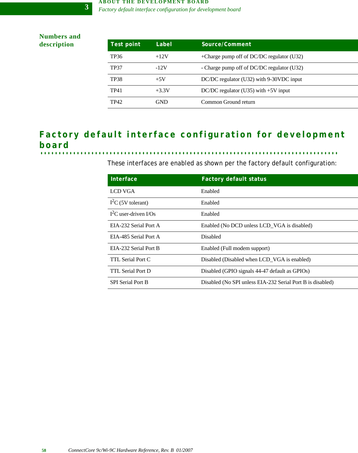
![WHAT’S ON THE MODULE?Edge connector, P322 ConnectCore 9c/Wi-9C Hardware Reference, Rev. B 01/2007276 GPIO[07] DCD_B ENBL_B IRQ1 IRQ1: Duplicate on GPIO[28] and GPIO[65]77 GPIO[11] CTS_A TIMER0IRQ2 TIMER0: Primary on GPIO[02]IRQ2: Primary on GPIO[32]78 GPIO[06] RI_B CLK_B PFAULT# TIMER7 PFAULT: Primary on GPIO[16]TIMER7: Primary on GPIO[31]79 GPIO[10] BS: ND2 RTS_A PWM0 PWM0: Primary on GPIO[36]80 GPIO[05] DSR_B PERR81 GND Common GND return82 GND Common GND return83 GPIO[09] RXD_A DIN_A84 GPIO[04] BS: ND0 DTR_B PBUSY85 GPIO[08] BS: ND1 TXD_A DOUT_A86 GPIO[03] CTS_B PACK#87 GPIO[19] BS: PLL_BYP CLLP/HSYNC PLL_BYP: Reserved. Do not pull down88 GPIO[02] BS: FS1 RTS_B TIMER0 TIMER0: Duplicate on GPIO[11]89 GPIO[18] CLPOWER IRQ3 IRQ3: Primary on GPIO[40]90 GPIO[01] RXD_B DIN_B IRQ0 IRQ0: Duplicate on GPIO[13] and GPIOP[68]91 OE# Output enable Wi-9C onlyCC9C: Reserved92 GPIO[00] BS: FS0 TXD_B DOUT_B TIMER1 TIMER1: Primary on GPIO[14]93 GND Common GND return94 GND Common GND return95 WE# Write enable Wi-9C onlyCC9C: Reserved96 GPIO[49] BS: CS_POL SPD PLH97 CS# Chip select Wi-9C onlyCC9C: Reserved98 GPIO[48] SUSP PSELI99 TXB+R Ethernet Reserved100 TXA+R Ethernet Reserved101 GND Common GND return102 GND Common GND return103 TXB-R Ethernet Reserved104 TXA-R Ethernet Reserved105 RST# System Hardware reset (input; active LOW; minimum pulse width 10uS)106 ACT_LED# Ethernet Reserved107 BOOTMUXR# System ReservedDimm Pin Signal BootStrap (BS) / System / Other UART SPI I2C USB LCD IEEE 1284 PWM / Timer / IRQNotes](https://usermanual.wiki/Digi/50M1355/User-Guide-781539-Page-32.png)
![. . . . .WHAT’S ON THE MODULE?Edge connector, P3www.digiembedded.com 23108 LNK_LED Ethernet Wi-9C onlyCC9C: Reserved109 GPIO[16] OVRH# PFAULT# PWM0 OVRH#: USB overcurrent input. Available as GPIO on modules with USB hub or Ethernet only. Not available as GPIO if an external Host USB port is implemented using DM1 and DP1.PFAULT#: Primary on GPIO[06]PWM0: Duplicate on GPIO[10]110 ADDRESS_6 Address bus Wi-9C onlyCC9C: Reserved111 GPIO[17] ND4 PONH# PONH#: USB power on output. Available as GPIO on modules with USB hub or Ethernet only. Not available as GPIO if an external Host USB port is implemented using DM1 and DP1.112 ADDRESS_7 Address bus Wi-9C onlyCC9C: Reserved113 OVR3# USB port 3 overcurrentReserved for future use; no connect114 OVR4# USB port 4 overcurrentReserved for future use; no connect115 PON3# USB port 3 power-onReserved for future use; no connect116 PON4# USB port 4 power-onReserved for future use; no connect117 OVR1# USB port 1 overcurrentReserved for future use; no connect118 OVR2# USB port 2 overcurrentReserved for future use; no connect119 PON1# USB port 1 power-onReserved for future use; no connect120 PON2# USB port 2 power-onReserved for future use; no connect121 GND Common GND return122 GND Common GND return123 DM4 USB port 4 data (-)Reserved for future use; no connect124 DP4 USB port 4 data (+)Reserved for future use; no connect125 GND Common GND return126 GND Common GND return127 DM3 USB port 3 data (-)Reserved for future use; no connect128 DP3 USB port 3 data (+)Reserved for future use; no connect129 GND Common GND returnDimm Pin Signal BootStrap (BS) / System / Other UART SPI I2C USB LCD IEEE 1284 PWM / Timer / IRQNotes](https://usermanual.wiki/Digi/50M1355/User-Guide-781539-Page-33.png)
![WHAT’S ON THE MODULE?Edge connector, P324 ConnectCore 9c/Wi-9C Hardware Reference, Rev. B 01/20072Pin assignment by GPIO130 GND Common GND return131 DM2 USB port 2 data (-)Reserved for future use; no connect132 DP2 USB port 2 data (+)Reserved for future use; no connect133 GND Common GND return134 GND Common GND return135 DM1 USB port 1 data (-)Reserved for future use; no connect136 DP1 USB port 1 data (+)Reserved for future use; no connect137 GND Common GND return138 GND Common GND return139 +5V Power to USB, if used (Used only with a module with on-board USB)140 +5V Power to USB, if used (Used only with a module with on-board USB)141 +5V Power to USB, if used (Used only with a module with on-board USB)142 +5V Power to USB, if used (Used only with a module with on-board USB)143 GND Common GND return144 GND Common GND returnDimm Pin Signal BootStrap (BS) / System / Other UART SPI I2C USB LCD IEEE 1284 PWM / Timer / IRQNotesSignal SO-DIMM BootStrap (BS / System / OtherUART SPI I2C USB LCD IEEE 1284 PWM / Timer / IRQNotesGPIO[00] 92 BS: FS0 TXD_B DOUT_B TIMER1 TIMER1: Primary on GPIO[14]GPIO[01] 90 RXD_B DIN_B IRQ0 IRQ0: Duplicate on GPIO[13] and GPIOP[68]GPIO[02] 88 BS: FS1 RTS_B TIMER0 TIMER0: Duplicate on GPIO[11]GPIO[03] 86 CTS_B PACK#GPIO[04] 84 BS: ND0 DTR_B PBUSYGPIO[05] 80 DSR_B PERRGPIO[06] 78 RI_B CLK_B PFAULT# TIMER7 PFAULT: Primary on GPIO[16]TIMER7: Primary on GPIO[31]GPIO[07] 76 DCD_B ENBL_B IRQ1 IRQ1: Duplicate on GPIO[28] and GPIO[65]GPIO[08] 85 BS: ND1 TXD_A DOUT_AGPIO[09] 83 RXD_A DIN_A](https://usermanual.wiki/Digi/50M1355/User-Guide-781539-Page-34.png)
![. . . . .WHAT’S ON THE MODULE?Edge connector, P3www.digiembedded.com 25GPIO[10] 79 BS: ND2 RTS_A PWM0 PWM0: Primary on GPIO[36]GPIO[11] 77 CTS_A TIMER0IRQ2 TIMER0: Primary on GPIO[02]IRQ2: Primary on GPIO[32]GPIO[12] 75 BS: ND3 DTR_A PWM1 PWM1: Primary on GPIO[37]GPIO[13] 73 DSR_A PWM2IRQ0 PWM2: Primary on GPIO[38]IRQ0: Primary on GPIO[01]GPIO[14] 69 RI_A CLK_A PWM3TIMER1 PWM3: Primary on GPIO[39]TIMER1: Duplicate on GPIO[00]GPIO[15] 67 DCD_A ENBL_A LCDCLKI TIMER2GPIO[16] 109 OVRH# PFAULT# PWM0 OVRH#: USB overcurrent input. Available as GPIO on modules with USB hub or Ethernet only, and not required for external USB Host support. PFAUL#T: Primary on GPIO[06]PWM0: Duplicate on GPIO[10]GPIO[17] 111 ND4 PONH# PONH#: USB power on output. Available as GPIO on modules with USB hub or Ethernet only, and not required for external USB Host support.GPIO[18] 89 CLPOWER IRQ3 IRQ3: Primary on GPIO[40]GPIO[19] 87 BS: PLL_BYP CLLP/HSYNC PLL_BYP: Reserved. Do not pull downGPIO[20] 46 BS: CS1_LSB DTR_C CLCP/LDCCLKO GPIO[20]: Output drive 8mAGPIO[21] 44 DSR_C CLFP VSYNCGPIO[22] 42 RI_C CLK_C CLACGPIO[23] 38 DCD_C ENBL_C CLLEGPIO[24] 37 BS:CS1_MSB DTR_D CLD0GPIO[25] 35 DSR_D CLD1GPIO[26] 33 RI_D CLK_D CLD2 TIMER3GPIO[27] 31 DCD_D ENBL_D CLD3 TIMER4GPIO[28] 65 CLD4(CLD8) IRQ1 CLD8: Primary on GPIO[32]IRQ1: Primary on GPIO[07]GPIO[29] 74 CLD5(CLD9) TIMER5 CLD9: Primary on GPIO[33]GPIO[30] 63 CLD6(CLD10) TIMER6 CLD10: Primary on GPIO[34]GPIO[31] 70 CLD7(CLD11) TIMER7 CLD11: Primary on GPIO[35]TIMER7: Duplicate on GPIO[06]GPIO[32] 57 CLD8 PD1 IRQ2 CLD8: Duplicate on GPIO[28]IRQ2: Duplicate on GPIO[11]GPIO[33] 68 CLD9 PD2 CLD9: Duplicate on GPIO[29]Signal SO-DIMM BootStrap (BS / System / OtherUART SPI I2C USB LCD IEEE 1284 PWM / Timer / IRQNotes](https://usermanual.wiki/Digi/50M1355/User-Guide-781539-Page-35.png)
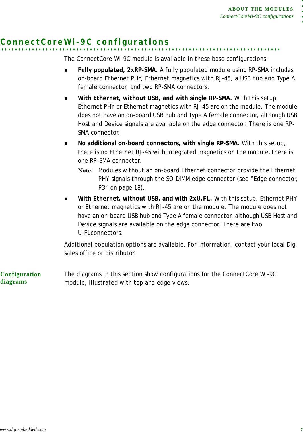
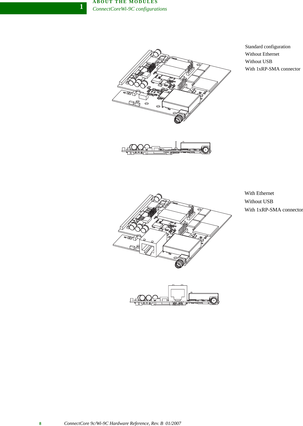
![WHAT’S ON THE MODULE?Antenna connectors: RP/SMA and U.FL (ConnectCore Wi-9C only)26 ConnectCore 9c/Wi-9C Hardware Reference, Rev. B 01/20072Antenna connectors: RP/SMA and U.FL (ConnectCore Wi-9C . . . . . . . . . . . . . . . . . . . . . . . . . . . . . . . . . . . . . . . . . . . . . . . . . . . . . . . . . . . . . . . . . . . . . . . . . . . . . . . . . .only)The ConnectCore Wi-9C supports two types of antenna connectors: RP-SMA and U.FL. The standard connector population option is 1 RP-SMA connector. Dual diversity operation and custom connector populations are available.GPIO[35] 66 SDA CLD11 PD4 SDA: Duplicate on GPIO[71]CLD11: Primary on GPIO[13]GPIO[36] 53 CLD12 PD5 PWM0 PWM0: Duplicate on GPIO[10]GPIO[37] 64 CLD13 PD6 PWM1 PWM1: Duplicate on GPIO[12]GPIO[38] 51 CLD14 PD7 PWM2 PWM2: Duplicate on GPIO[13]GPIO[39] 58 CLD15 PD8 PWM3 PWM3: Duplicate on GPIO[14]GPIO[40] 56 TXD_C DOUT_C CLD16 IRQ3 IRQ3: Duplicate on GPIO[18]GPIO[41] 54 RXD_C DIN_C CLD17GPIO[42] 52 RTS_C DATA+ Add 10-15K pullup if not usedGPIO[43] 48 CTS_C DATA- PDIR Add 10-15K pullup if not usedGPIO[44] 47 BS: EndianPull down for Big EndianTXD_D DOUT_D OE PSELOGPIO[45] 45 RXD_D DIN_D RCV PSTB#GPIO[46] 43 RTS_D RXD+ PAFD# RXD+: Only used for unidirectional PHYGPIO[47] 41 CTS_D RXD- PINIT# RXD-: Only used for unidirectional PHYGPIO[48] 98 SUSP PSELIGPIO[49] 96 BS: CS_POL SPD PLHGPIO[66] 36 CR2: Yellow user LEDOutput drive 8mAGPIO[67] 34 CR1: Green user LEDOutput drive 8mAMFGO_CR1GPIO[68] NC No connectGPIO[69] 28 IRQ1 GPIO[69]: Output drive 8mAIRQ1: Primary on GPIO[07]Add 10-15K pullup if not usedGPIO[70] 26 iic_scl GPIO[70]: Output drive 8mAiic_scl: Primary on GPIO[34]GPIO[71] 24 iic_sda GPIO[71]: Output drive 8mAiic_sda: Primary on GPIO[35]MFGI_GPIO[72] 22 ReservedSignal SO-DIMM BootStrap (BS / System / OtherUART SPI I2C USB LCD IEEE 1284 PWM / Timer / IRQNotes](https://usermanual.wiki/Digi/50M1355/User-Guide-781539-Page-36.png)


![. . . . .MODULE SPECIFICATIONSPower requirementswww.digiembedded.com 67. . . . . . . . . . . . . . . . . . . . . . . . . . . . . . . . . . . . . . . . . . . . . . . . . . . . . . . . . . . . . . . . . . . . . . . . . . . . . . . . . .Power requirementsConnectCore 9C Module: 3.3VDC @ 0.75A maxUSB interface: 5VDC @ 0.5A max per port (optional)ConnectCoreWi-9CModule: 3.3V ± 5% @ 0.95A max, 0.70A typOptional USB: 5V ± 10% @ 1.0A maxPower up The rise time of both the 3.3V power supply and 5V power supply must be between 700 μs and 140 ms, and the inrush current must be limited to less than 2A.. . . . . . . . . . . . . . . . . . . . . . . . . . . . . . . . . . . . . . . . . . . . . . . . . . . . . . . . . . . . . . . . . . . . . . . . . . . . . . . . . .Real-time clockThe accuracy of the internal Real-Time Clock on the module’s processor is .15%.. . . . . . . . . . . . . . . . . . . . . . . . . . . . . . . . . . . . . . . . . . . . . . . . . . . . . . . . . . . . . . . . . . . . . . . . . . . . . . . . . .I2C signalsThe I2C signals are multiplexed with GPIO.Legend SO-DIMM pin #: Pin number assignment for signal Signal: Pin name for each signal. U/D: Indicates whether the pin has an internal pullup resistor or pulldown resistor.•U — Pullup•D— Pulldown•Blank — Neither an internal pullup or pulldown resistor OD (mA): The output drive of an output buffer. I/O: Type of signal input (I), output (O), or input/output (I/O)Signals SO-DIMM Pin# Signal name GPIO U/D OD (mA) I/O Description55 iic_scl GPIO[34] U 4 I/O I2C serial clock line.Duplicate on GPIO[70]66 iic_sda GPIO[35] U 4 I/O I2C serial data line.Duplicate on GPIO[71]](https://usermanual.wiki/Digi/50M1355/User-Guide-781539-Page-77.png)
![MODULE SPECIFICATIONSUSB interface68 ConnectCore 9C/Wi-9C Hardware Reference, Rev. B 01/2007A. . . . . . . . . . . . . . . . . . . . . . . . . . . . . . . . . . . . . . . . . . . . . . . . . . . . . . . . . . . . . . . . . . . . . . . . . . . . . . . . . .USB interfaceUSB Host The USB Host consists of a USB Host controller that conforms to the Open Host Controller Interface (OHCI) specification and a wrapper to interface the module to the rest of the system. The USB Host interfaces to the internal USB PHY provided by the NS9360, and is connected to an optional hub on the module.)USB Device The USB Device module provides a USB 2.0-compliant interface for both full-speed (12Mbps) and low-speed (1.5 Mbps) operation. The module supports one bidirectional endpoint and up to 10 unidirectional endpoints that can be individually programmed for endpoint type (interrupt, bulk, or isochronous) and direction. Each endpoint is assigned to a DMA channel in a multi-channel BBus DMA controller. The USB Device module interfaces to either the internal NS9360 USB PHY or an external USB PHY using GPIO.Support Both USB Host and Device can be supported at the same time:USB Device, in this case, must use the only the signals shown in the table in the section "USB Device only," beginning on page 69.USB Host can be on the module or external to the module. If USB Host is external to the module, use only the signals shown in the table in the section "No USB on module," beginning on page 68.Note:All output drivers for USB meet the standard USB driver specifications.USB Host with hub on moduleConnect up to two ports using the dual USB connector, P6.All hub signals out to the SO-DIMM edge connector, P3, are reserved for future use.No USB on moduleUSB data lines are brought out on DM1 and DP1. –Terminate DM1 and DP1 with 15K pulldowns, if not used.OVR1# and PON1# are multiplexed with GPIO16 and GPIO17.26 iic_scl GPIO[70] 8 I/O I2C serial clock line.Primary on GPIO[34]24 iic_sda GPIIO[71] 8 I/O I2C serial data line.Primary on GPIO[35]SO-DIMM Pin# Signal name GPIO U/D OD (mA) I/O Description](https://usermanual.wiki/Digi/50M1355/User-Guide-781539-Page-78.png)
![. . . . .MODULE SPECIFICATIONSModule resetwww.digiembedded.com 69Can be used as Host or Device (USB PHY is internal)USB Device only The USB Device interface only requires an external PHY. The USB signals are multiplexed with GPIOs. On the Digi development board, these functions are lost:Serial Port D: TXDD, RXDD, RTSD#, AND CTSD# on GPIO[44], GPIO[45], GPIO[46], and GPIO[47]Serial Port C: RTSC# and CTSC# on GPIO[42] and GPIO[43]User LED3 and LED4 on GPIO[48] and GPIO[49]. . . . . . . . . . . . . . . . . . . . . . . . . . . . . . . . . . . . . . . . . . . . . . . . . . . . . . . . . . . . . . . . . . . . . . . . . . . . . . . . . .Module reset The module reset pin is on the module SO-DIMM connector, P3 — pin 105, signal RST#.Active low signal. An ADM811S voltage supervisor is provided to reset the ConnectCore 9C module at any time the power phases out. If +3.3V power supply dips below 2.93 volts, the ADM811S asserts and holds the reset signal. SO-DIMM pin # Signal name I/O Description135 DM1 I/O USB data -136 DP1 I/O USB data+109 OVRH# / gpio16 I Overcurrent111 PONH# / gpio17 O Power-onSO-DIMM pin Signal name I/O Description48 DATA- / GPIO[43] I/O USB VM52 DATA+ / GPIO[42] I/O USB VP47 OE / GPIO[44] O USB OE45 RCV / GPIO[45] I USB RCV43 RXD+ / GPIO[46] I/O USB RXP/EMUN41 RXD- / GPIO[47] I USB RXM (unidirectional only)96 SPD / GPIO[49] O USB SPD98 SUSP / GPIO[48] O USB SUSP](https://usermanual.wiki/Digi/50M1355/User-Guide-781539-Page-79.png)
![. . . . .MODULE SPECIFICATIONSModule / SO-DIMM signal characteristicswww.digiembedded.com 7110 DATA_1 12 BI Data bus signal 411 DATA_2 12 BI Data bus signal 412 DATA_3 12 BI Data bus signal 413 DATA_4 12 BI Data bus signal 414 DATA_5 12 BI Data bus signal 415 DATA_6 12 BI Data bus signal 416 DATA_7 12 BI Data bus signal 417 ADDRESS_0 12 O Address bus signal 418 ADDRESS_1 12 O Address bus signal 419 GND20 GND21 ADDRESS_2 12 O Address bus signal 422 MFGI_GPIO[72] 8 I/O 123 ADDRESS_3 12 O Address bus signal 424 GPIO[71] 8 I/O 125 ADDRESS_4 12 O Address bus signal 426 GPIO[70] 8 I/O 127 ADDRESS_5 12 O Address bus signal 428 GPIO[69] 8 I/O 129 GND30 GND31 GPIO[27] U 4 I/O 232 No connect33 GPIO[26] U 4 I/O 234 GPIO[67] 8 I/O 135 GPIO[25] U 4 I/O 236 GPIO[66] 8 I/O 137 GPIO[24] U 4 I/O 3 BS: Chip select 1 data width bootstrap select (Default=0, 16-bit width)38 GPIO9230 U 4 I/O 239 GND40 GND41 GPIO[47] U 2 I/O 2Pin SIgnal name Internal U/D OD (mA) I/O Description I/O class Notes / Bootstrapping (BS)](https://usermanual.wiki/Digi/50M1355/User-Guide-781539-Page-81.png)
![MODULE SPECIFICATIONSModule / SO-DIMM signal characteristics72 ConnectCore 9C/Wi-9C Hardware Reference, Rev. B 01/2007A42 GPIO[22] U 4 I/O 243 GPIO[46] U 2 I/O 244 GPIO[21] U 4 I/O 245 GPIO[45] U 2 I/O 246 GPIO[20] U 8 I/O 3 BS: Chip select 1 data width bootstrap select (Default=0, 16-bit width)47 GPIO[44] U 2 I/O 3 BS: Endian mode (Default=0, Big Endian)48 GPIO[43] 2 I/O 149 GND50 GND51 GPIO[38] U 4 I/O 252 GPIO[42] 2 I/O 153 GPIO[36] U 4 I/O 254 GPIO[41] U 4 I/O 255 GPIO[34] U 4 I/O 256 GPIO[40] U 4 I/O 257 GPIO[32] U 4 I/O 258 GPIO[39] U 4 I/O 259 GND60 GND61 GND62 GND63 GPIO[30] U 4 I/O 264 GPIO[37] U 4 I/O 265 GPIO[28] U 4 I/O 266 GPIO[35] U 4 I/O 267 GPIO[15] U 2 I/O 268 GPIO[33] U 4 I/O 269 GPIO[14] U 2 I/O 270 GPIO[31] U 4 I/O 271 GND72 GNDPin SIgnal name Internal U/D OD (mA) I/O Description I/O class Notes / Bootstrapping (BS)](https://usermanual.wiki/Digi/50M1355/User-Guide-781539-Page-82.png)
![. . . . .MODULE SPECIFICATIONSModule / SO-DIMM signal characteristicswww.digiembedded.com 7373 GPIO[13] U 2 I/O 274 GPIO[29] U 2 I/O 275 GPIO[12] U 2 I/O 3 BS: PLL_ND[3] (Default=0, PLL multiplier)76 GPIO[07] U 2 I/O 277 GPIO[11] U 2 I/O 278 GPIO[06] U 2 I/O 279 GPIO[10] U 2 I/O 3 BS: PLL_ND[2] (Default=0, PLL multiplier)80 GPIO[05] U 2 I/O 281 GND82 GND83 GPIO[09] U 2 I/O 284 GPIO[04] U 2 I/O 2 BS: PLL_ND[4] (Default=1, PLL multiplier)85 GPIO[08] U 2 I/O 3 BS: PLL_ND[1] (Default=0, PLL multiplier)86 GPIO[03] U 2 I/O 287 GPIO[19] U 4 I/O 2 BS: PLL_BYP (This pin must not be pulled to logic 0 during Boot)88 GPIO[02] U 2 I/O 3 BS: PLL_FS[0] (Default=0, PLL frequency divide by 1)89 GPIO[18] U 4 I/O 290 GPIO[01] U 2 I/O 291 OE# 24 O Output enable92 GPIO[00] U 2 I/0 3 BS: PLL_FS[0] (Default=0, PLL frequency divide by 1)93 GND94 GND95 WE# 24 O Write enable96 GPIO[49] U 2 I/O 2 BS: CS_POL (Chip select polarity, 0=Active high, 1=Active low)97 CS# 24 O Chip select98 GPIO[48] U 2 I/O 299 TXB+R I/O Remote Ethernet TX B+100 TXA+R I/O Remote Ethernet TX A+Pin SIgnal name Internal U/D OD (mA) I/O Description I/O class Notes / Bootstrapping (BS)](https://usermanual.wiki/Digi/50M1355/User-Guide-781539-Page-83.png)
![MODULE SPECIFICATIONSModule / SO-DIMM signal characteristics74 ConnectCore 9C/Wi-9C Hardware Reference, Rev. B 01/2007A101 GND102 GND103 TXB-R I/O Remote Ethernet TX B-104 TXA-R I/O Remote Ethernet TX A-105 MODRST# I Reset 1106 ACT_LED# I PHY activity LED107 BOOTMUXR# O Boot mux108 LNK_LED I PHY link LED109 GPIO[16] U 2 I/O 2110 ADDRESS_6 12 O Address bus signal 4111 GPIO[17] U 2 I/O 2 BS: PLL_ND[4] (Default=1, PLL multiplier)112 ADDRESS_7 12 O Address bus signal 4113 OVR3# I USB over-current 3114 OVR4# I USB over-current 4115 PON3# 4 O USB power-on 3116 PON4# 4 O USB power-on 4117 OVR1# I USB over-current 1118 OVR2# I USB over-current 2119 PON1# 4 O USB power-on 1120 PON2# 4 O USB power-on 2121 GND122 GND123 DM4 I/O USB data-124 DP4 I/O USB data+125 GND126 GND127 DM3 I/O USB data-128 DP3 I/O USB data+129 GND130 GND131 DM2 I/O USB data-132 DP2 I/O USB data+Pin SIgnal name Internal U/D OD (mA) I/O Description I/O class Notes / Bootstrapping (BS)](https://usermanual.wiki/Digi/50M1355/User-Guide-781539-Page-84.png)

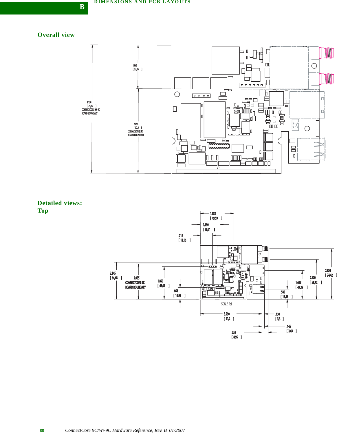
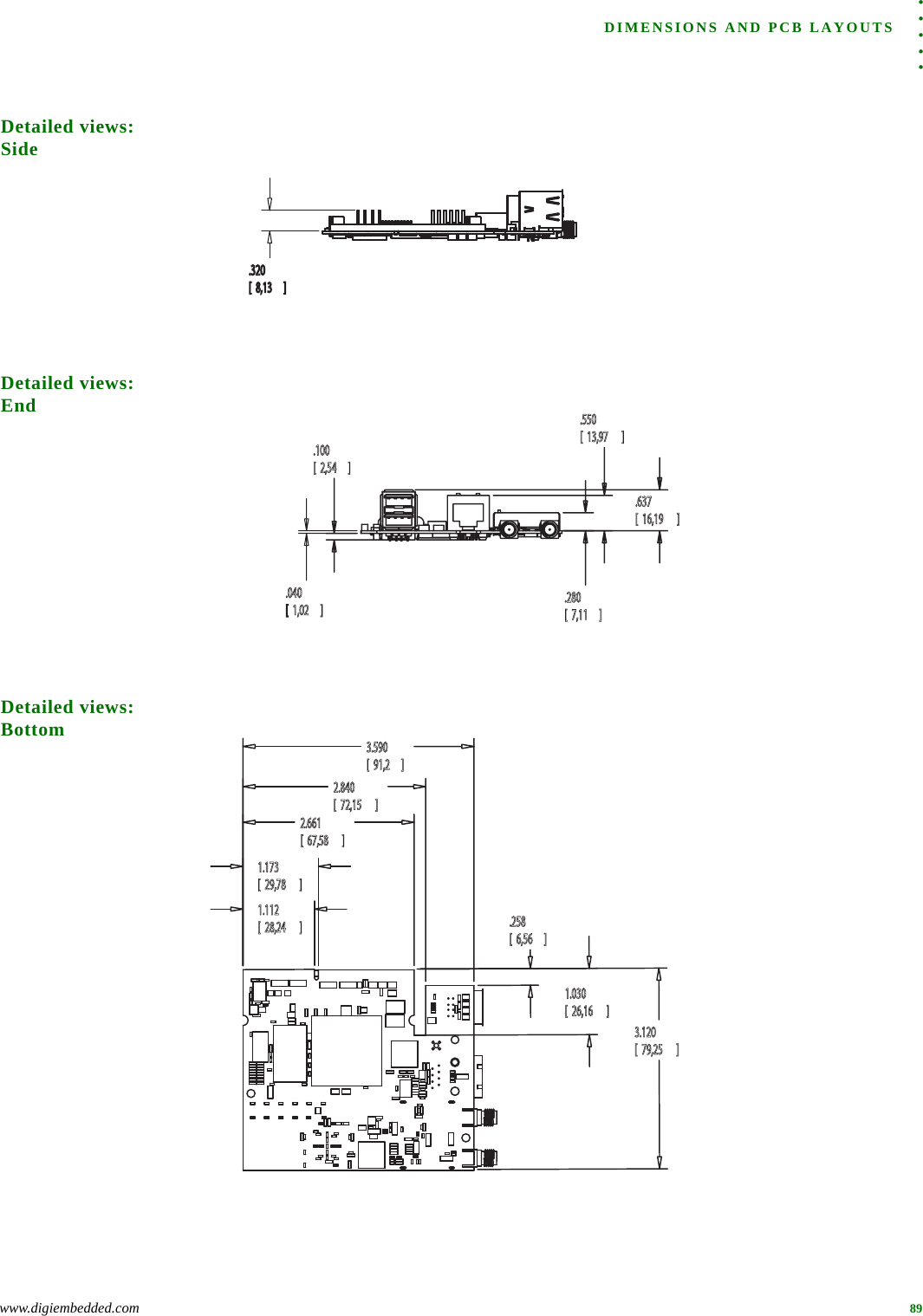
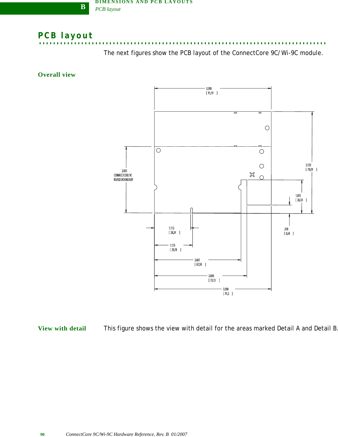
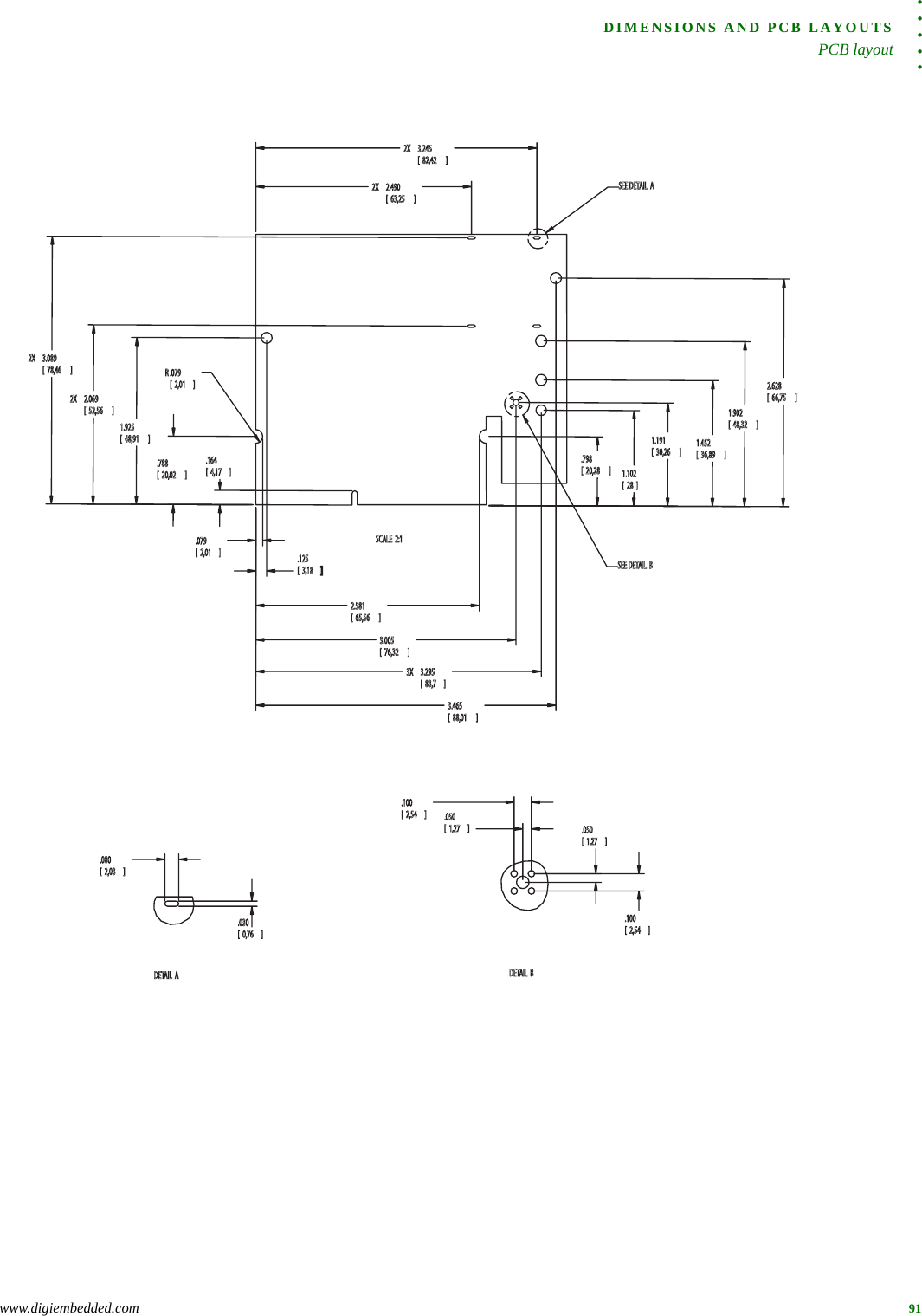
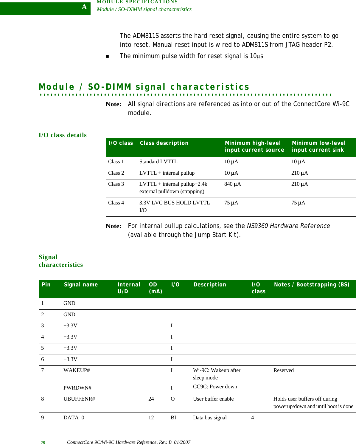
![87Dimensions and PCB LayoutsAPPENDIX BThis appendix shows the dimensions of each module, as well as PCB (printed circuit board) layouts of each.Module dimensions The next figures show the dimensions of the ConnectCore 9C/Wi-9C module. Dimensions are in inches and millimeters (millimeter size is in brackets [ ]).These are the tolerances for the drawings shown in this section:Measure Tolerance.XX ± .02.XXX ± .010Angles ± 2 degrees](https://usermanual.wiki/Digi/50M1355/User-Guide-781539-Page-97.png)