Digi 50M1355 Communication Bridge User Manual ConnectCore 9C Wi 9C Hardware Reference
Digi International Inc Communication Bridge ConnectCore 9C Wi 9C Hardware Reference
Digi >
Users Manual

Part number/version: 90000789_B
Release date: January 2007
www.digiembedded.com
ConnectCore™ 9C/Wi-9C
. . . . . . . . . . . . . . . . . . . . . . . . . . . . . . . . . . . . . . . . . . . . . . . . . . . . . . . . . . . . . . . . .
.
Hardware Reference
Digi International, Inc.
11001 Bren Road East
Minnetonka, MN 55343 U.S.A.
United States: +1 877 912-3444
Other locations: +1 952 912-3444
www.digiembedded.com
©2005-2007 Digi International Inc.
Printed in the United States of America. All rights reserved.
Digi, Digi International, the Digi logo, NetSilicon, a Digi International Company, Jump Start Kit,
ConnectCore, NET+, NET+OS and NET+Works are trademarks or registered trademarks of Digi
International, Inc. in the United States and other countries worldwide. All other trademarks are the
property of their respective owners.
Information in this document is subject to change without notice and does not represent a committment
on the part of Digi International.
Digi provides this document “as is,” without warranty of any kind, either expressed or implied, including,
but not limited to, the implied warranties of, fitness or merchantability for a particular purpose. Digi may
make improvements and/or changes in this manual or in the product(s) and/or the program(s) described
in this manual at any time.
This product could include technical inaccuracies or typographical errors. Changes are made periodically
to the information herein; these changes may be incorporated in new editions of the publication.

iii
Contents
.
. . . . . . . . . . . . . . . . . . . . . . . . . . . . . . . . . . . . . . . . . . . . . . . . . . . . . . . . . . . . . . . . . . . .
Chapter 1: About the Modules ...............................................................1
Common module features...............................................................1
Wi-9C specific features..................................................................2
Memory.....................................................................................2
Memory clocks ............................................................................2
Other system clocks......................................................................2
Interfaces.........................................................................................2
Ethernet....................................................................................2
WLAN .......................................................................................3
USB 2.0 Host and Device.................................................................3
Serial .......................................................................................4
I2C ..........................................................................................4
External Memory bus.....................................................................4
LCD..........................................................................................4
ConnectCore 9C configurations ...............................................................5
Configuration diagrams..................................................................5
ConnectCoreWi-9C configurations ............................................................7
Configuration diagrams..................................................................7
Chapter 2: What’s on the Module? ......................................................11
Module layout.................................................................................. 11
Ethernet connector ........................................................................... 12
Ethernet connector pins............................................................... 12
Ethernet LEDs ........................................................................... 12
802.3af Power over Ethernet (PoE) pass-through
connector, P5 .................................................................................. 13
Connector description ................................................................. 13
PoE support.............................................................................. 13
Module LEDs.................................................................................... 14
Description .............................................................................. 14
ConnectCore
Wi-9C default use....................................................................... 14
JTAG 20-pin header connector, P2 ......................................................... 15
Pin assignment.......................................................................... 15
JTAG adapter assembly....................................................................... 16
JTAG adapter............................................................................ 16

iv ConnectCore 9C/Wi-9C Hardware Reference, Rev B 01/2007
Assembly .................................................................................17
USB Host connector, P6.......................................................................18
Edge connector, P3............................................................................18
Pin assignment ..........................................................................18
Pin assignment by SO-DIMM pin number ............................................19
Pin assignment by GPIO................................................................24
Antenna connectors: RP/SMA and U.FL (ConnectCore Wi-9C only)....................26
RP-SMA connectors, P10 and P8......................................................27
U.FL connectors, P11 and P9 .........................................................27
Chapter 3: About the Development Board ........................................29
Features..................................................................................29
Basic description...............................................................................30
Switches and buttons .........................................................................31
Serial Port A switch, SW1..............................................................31
Serial Port B switch, SW2..............................................................32
User pushbuttons, SW3 and SW4 .....................................................32
Power switch, SW5 .....................................................................32
Hardware Reset button, SW6 .........................................................32
VGA (enable) switch, SW7.............................................................32
I2C and SPI header connectors ..............................................................33
I2C header connector, P8 .............................................................33
SPI header connector, P7..............................................................34
Serial port connectors ........................................................................35
Serial port A (EIA-232/422/485) connector, P13...................................35
Serial port B (EIA-232) connector, P9 ...............................................36
Serial port C header connector, P10.................................................37
P10 connector pin assignment........................................................37
Serial port D header connector, P11.................................................37
VGA connector / External LCD clock .......................................................39
VGA connector, P6 .....................................................................39
External LCD clock, G1 ................................................................40
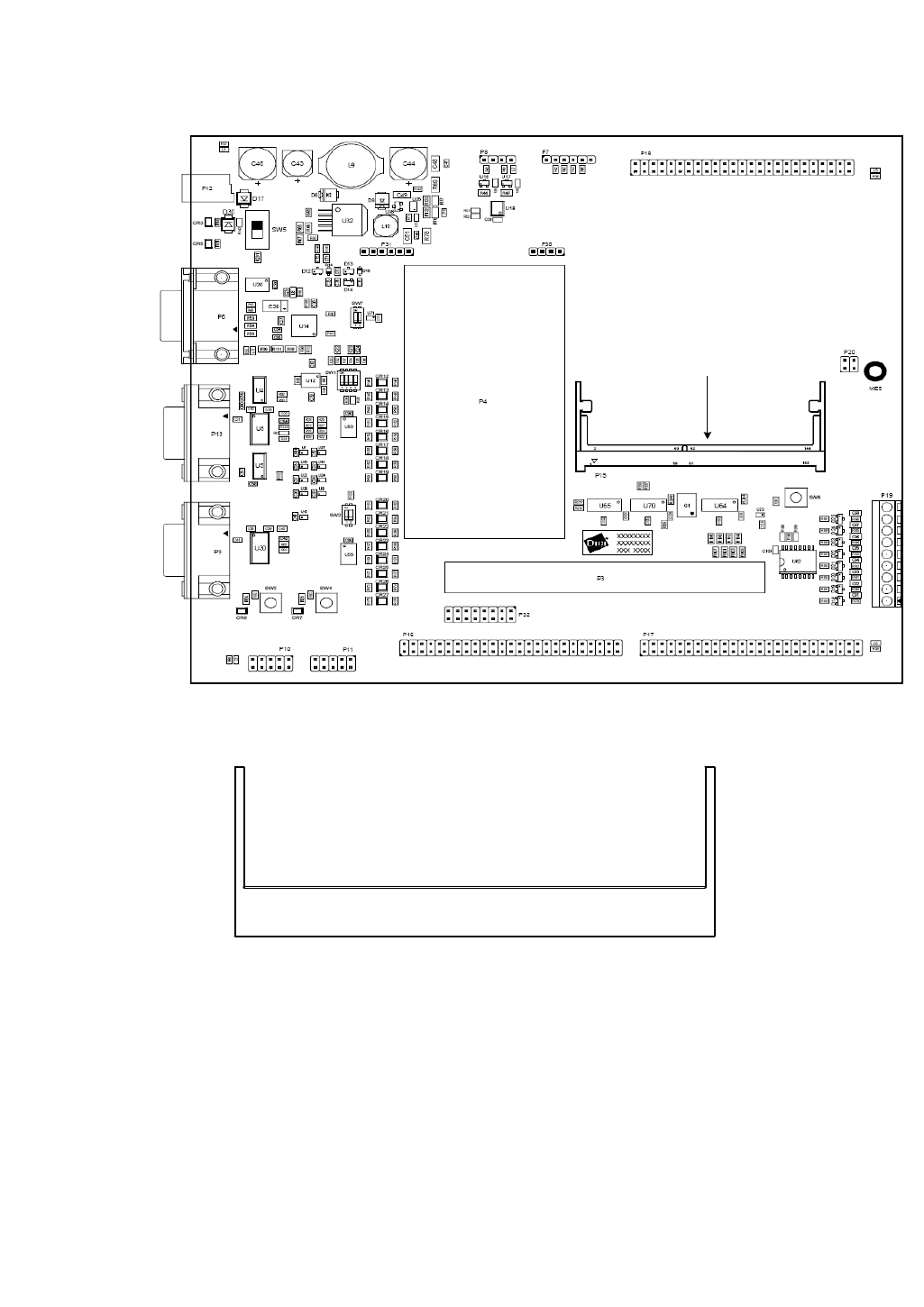
Development board SO-DIMM connector, P15.............................................40
Bird’s-eye view..........................................................................41
Close-up..................................................................................41
Inserting the module into the SO-DIMM connector ................................41
Application-specific expansion headers — P16 and P17 .................................43
Peripheral application board header, P16..........................................44
Platform application board header, P17............................................45
LCD application board header, P18.........................................................46
USB Device application header, P32........................................................48
P32 pin assignment.....................................................................48
Digital I/O, P19 ................................................................................49
Power over Ethernet (PoE) connectors.....................................................50

. . . . .
www.digiembedded.com v
802.3afPoE connector, P20............................................................51
P30 connector ...........................................................................51
P31 connector ...........................................................................51
Through-hole prototyping (wrap-field) area, P3 and P4.................................52
Through-hole signal rail, P3...........................................................52
Wrap-field area, P4.....................................................................53
Development board LEDs .....................................................................54
Power LEDs, CR3 and CR5 .............................................................54
User LEDs, CR6 and CR7................................................................54
Serial LEDs ...............................................................................54
Current Measurement Option (CMO)........................................................55
How the CMO works ....................................................................56
Power jack, P12................................................................................57
Test points......................................................................................57
Numbers and description ..............................................................58
Factory default interface configuration for development board.......................58
Chapter 4: LCD and USB Configuration ...........................................59
LCD displays ....................................................................................59
Control and data pins ..................................................................59
LCD controller control pins............................................................60
LCD controller data pins ...............................................................60
Colors and gray shades.................................................................60
Sample displays .........................................................................61
Resolution................................................................................61
Refresh frequency ......................................................................61
Sample applications ...........................................................................61
Default LCD controller .................................................................62
Formula...................................................................................62
Example 1: 18-bit VGA .................................................................62
USB configuration..............................................................................63
Appendix E: Module Specifications 65
Mechanical dimensions........................................................................65
ConnectCore
Wi-9C .....................................................................................65
Environmental information...................................................................66
ConnectCore 9C .........................................................................66
ConnectCore
Wi-9C .....................................................................................66
Network interface .............................................................................66
Ethernet..................................................................................66
WLAN......................................................................................66
Power requirements...........................................................................67

vi ConnectCore 9C/Wi-9C Hardware Reference, Rev B 01/2007
ConnectCore 9C.........................................................................67
ConnectCore
Wi-9C .....................................................................................67
Power up.................................................................................67
Real-time clock ................................................................................67
I2C signals.......................................................................................67
USB interface...................................................................................68
USB Host .................................................................................68
USB Device...............................................................................68
Support...................................................................................68
USB Host with hub on module ........................................................68
No USB on module ......................................................................68
USB Device only.........................................................................69
Module reset ...................................................................................69
Module / SO-DIMM signal characteristics ..................................................70
I/O class details.........................................................................70
Signal characteristics ..................................................................70
Electrical characteristics.....................................................................75
Absolute maximum ratings............................................................75
Recommended operating conditions.................................................75
Power dissipation.......................................................................76
DC electrical characteristics.................................................................76
Inputs.....................................................................................76
Outputs...................................................................................76
USB internal PHY DC electrical inputs and outputs ......................................77
USB internal PHY DC electrical inputs...............................................77
USB internal PHY DC electrical outputs.............................................77
Antenna information ..........................................................................77
Antenna specifications — 2 dBi Dipole .....................................................78
Attributes ................................................................................78
Dimensions...............................................................................78
Antenna strength (radiation pattern) diagram.....................................79
Antenna specifications — 5 dBi Dipole .....................................................80
Attributes ................................................................................80
Dimensions (in mm) ....................................................................80
Radiation pattern: H-Plane (2.0 and 5.0 GHz) .....................................81
Radiation pattern: E-plane (2.0 and 5.0 GHz) .....................................82
Antenna specifications — 2 dBi PCB mount................................................82
Attributes ................................................................................83
Radiation patterns......................................................................83
FCC RF radiation exposure statement......................................................84
Safety statements .............................................................................84
Appendix F: Dimensions and PCB Layouts 87

. . . . .
www.digiembedded.com vii
Module dimensions......................................................................87
Overall view .............................................................................88
Detailed views: Top ....................................................................88
Detailed views: Side....................................................................89
Detailed views: End.....................................................................89
Detailed views: Bottom ................................................................89
PCB layout ......................................................................................90
Overall view .............................................................................90
View with detail.........................................................................90
Appendix G: Certifications 93
FCC Part 15 Class B............................................................................93


ix
Using this Guide
.
. . . . . . . . . . . . . . . . . . . . . . . . . . . . . . . . . . . . . . . . . . . . . . . . . . . . . . . . . . . . . . . . . . . .
This guide provides information about the Digi ConnectCore 9C and ConnectCore
Wi-9C embedded core modules.
Conventions used
in this guide This table describes the typographic conventions used in this guide:
. . . . . . . . . . . . . . . . . . . . . . . . . . . . . . . . . . . . . . . . . . . . . . . . . . . . . . . . . . . . . . . . . . . . . . . . . . . . . . . . . .
Digi information
Related
documentation For additional documentation, see the Documentation folder in the NET+OS Start
menu.
Documentation
updates Digi occasionally provides documentation updates on the Web site
(www.digiembedded.com/support).
Be aware that if you see differences between the documentation you received in
your package and the documentation on the Web site, the Web site content is the
latest version.
Support To get help with a question or technical problem with this product, or to make
comments and recommendations about our products or documentation, use the
contact information listed in this table:
This convention Is used for
italic type Emphasis, new terms, variables, and document titles.
monospaced type Filenames, pathnames, and code examples.
For Contact information
Technical support www.digiembedded.com/support
United States: +1 877 912-3444
Other locations: +1 952 912-3444


1
About the Modules
CHAPTER 1
The ConnectCore 9C and ConnectCore Wi-9C modules are powerful ARM9-based
modules in a compact and universal SO-DIMM (Small Outline Dual Inline Memory
Module) form factor. The modules provide core processing functionality with
integrated wired and wireless network connectivity and a complete set of
peripheral options in a footprint-compatible interchangeable SO-DIMM form factor
that allows you to optimize your system for either Ethernet, WLAN, or both.
The ConnectCore 9C provides 10/100 Ethernet connectivity only.
The ConnectCore Wi-9C provides both 10/100 Ethernet and 802.11b/g wireless
networking capabilities.
All modules are fully compliant with EU directive 2002/95/EC (RoHS).
Common module
features
32-bit NS9360 high performance RISC processor @ 155 MHz
Up to 256 MB Flash and 256 MB SDRAM
Compact SO-DIMM (Small Outline-Dual Inline Memory Module) design
Low power consumption
Industrial/extended operating temperature
10/100 Mbps Ethernet interface with optional on-board RJ-45 connector
IEEE802.3af compliant power pass-through (mid-span and end-span)
Up to four high-speed serial ports — UART and SPI mode configurable
I2C bus interface
USB 2.0 Host and Device interfaces
Optional on-board USB Host connector

ABOUT THE MODULES
Interfaces
2ConnectCore 9c/Wi-9C Hardware Reference, Rev. B 01/2007
1
Integrated LCD controller
Up to eight independent 16-/32-bit programmable timers, counters, or four
PWM functions
Four programmable external interrupts
Up to 55 shared General Purpose Input/Output (GPIO) ports
–Up to seven high-current (8mA) pins
8-bit wide data/address bus with external chip select
Processor-powered on-chip Real-Time Clock (RTC)
Population options available (processor speed, memory, connectors)
Wi-9C specific
features
802.11b/g WLAN interface
WEP, WPA, and WPA2/802.11i security standard
Single or dual-diversity antenna options
Memory The module’s standard memory configuration is 4 MB Flash and 16 MB SDRAM.
Memory clocks Memory clocks = 77.5 MHz
Not available for off-DIMM use
clk_out[0] — Not used; turned off by code
clk_out[1] — Connected to clk_in
clk_out[2] — Used for one bank of two X16 SDRAMS
clk_out[3] — Not used
Other system
clocks
Source clock is a 29.4912 MHz crystal or spread spectrum oscillator.
USB uses a 48.000 MHz oscillator
Ethernet versions have a 25.0000 MHz crystal
. . . . . . . . . . . . . . . . . . . . . . . . . . . . . . . . . . . . . . . . . . . . . . . . . . . . . . . . . . . . . . . . . . . . . . . . . . . . . . . . . .
Interfaces
The ConnectCore 9C/Wi-9C module supports several system interfaces. This section
details the features of these interfaces.
Ethernet The module provides a 10/100 Mbps Ethernet interface with optional on-board
RJ-45 connector and integrated LEDs. On modules not populated with the RJ-45
connector, the Ethernet PHY signals are available on the SO-DIMM edge connector.

. . . . .
ABOUT THE MODULES
Interfaces
www.digiembedded.com 3
Full-duplex or half-duplex
Station, broadcast, or multicast address filtering
2 kB RX FIFO
256-byte TX FIFO with on-chip buffer descriptor ring
Separate TX and RX DMA channels
Intelligent receive-side buffer size selection
Full statistics gathering support
External CAM filtering support
WLAN The ConnectCore Wi-9C provides integrated 802.11b/g wireless networking
capabilities.
Standard compliance: IEEE 802.11g-2003
Frequency: 2.4 GHz
Data rates: Up to 54 Mbps with fallback
Modulation:
DBPSK (1 Mbps)
DQPSK (2 Mbps)
CCK (5.5, 11 Mbps)
BPSK (6, 9 Mbps)
QPSK (12, 18 Mbps)
16-QAM (24, 36 Mbps)
64-QAM (48, 54 Mbps)
Transmit power: 12 dbm typical
Receive sensitivity: -73 dbm @ 54 Mbps and -87 dbm for 11Mbps
Antenna connectors: U.FL or RP-SMA
Dual-diversity: Available on modules with two U.FL or RP-SMA connectors
USB 2.0 Host and
Device
USB v2.0 full speed (12 Mbps) and low speed (1.5 Mbps)
Independent OHCI Host and Device ports
Internal USB PHY
External USB PHY interface
The module provides a population option for a four-port hub with onboard dual-
connector (500mA, 5V only) and full speed/low speed support.

ABOUT THE MODULES
Interfaces
4ConnectCore 9c/Wi-9C Hardware Reference, Rev. B 01/2007
1
Serial Bit rates from 75 bps to 921.6 kbps: asynchronous mode
Bit rates from 1.2 kbps to 11.25 Mbps: synchronous mode
UART provides:
–High performance hardware and software flow control
–Odd, even, or no parity
–5, 6, 7, or 8 bits
–1 or 2 stop bits
–Receive-side character and buffer gap timers
Four receive-side data match detectors
Two dedicated DMA channels per module; 8 channels total
32 byte TX FIFO and 32 byte RX FIFO per module
I2CI2C v.1.0 configurable to master or slave
Bit rates: fast (400 kHz) or normal (100 kHz) with clock stretching
7-bit and 10-bit address modes
Supports I2C bus arbitration
External Memory
bus
8-bit address bus
8-bit data bus
1 external chip select
Note:
The memory bus on the edge connector (P3) is available only on the
ConnectCore Wi-9C module.
LCD Dual 64-deep, 32-bit wide FIFOs for buffering incoming display data
Support for color and monochrome single- and dual-panel for Super Twisted
Nematic (STN) displays with 4- or 8-bit interfaces
Support for Thin Film Transistor (TFT) color displays
Resolution up to 800 x 600 pixels
15 gray-level mono, 3375 color STN, and 64K color TFT support
–Patented gray-scale algorithm
1, 2, or 4 bits-per-pixel (bpp) palettized displays for mono STN
1, 2, 4, or 8 bpp palettized color displays for STN and TFT
16 bpp true-color non-palettized, for color STN and TFT
Programmable timing for different display panels
256 entry, 16-bit palette RAM, arranged as a 128 x 32-bit RAM
. . . . .
ABOUT THE MODULES
ConnectCore 9C configurations
www.digiembedded.com 5
Frame, line, and pixel clock signals
AC bias signal for STN, data enable signal for TFT panels
Support for multiple data formats
. . . . . . . . . . . . . . . . . . . . . . . . . . . . . . . . . . . . . . . . . . . . . . . . . . . . . . . . . . . . . . . . . . . . . . . . . . . . . . . . . .
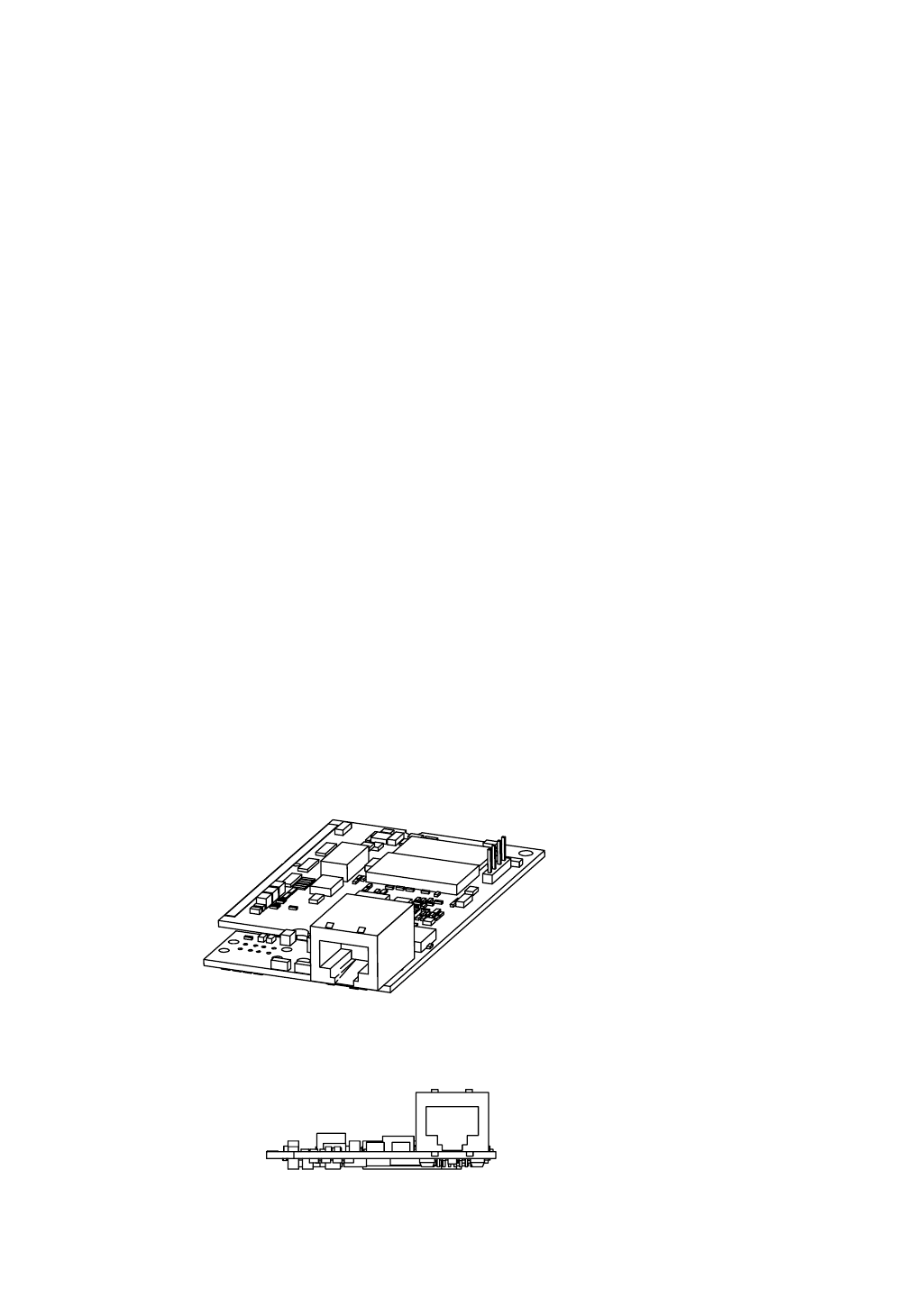
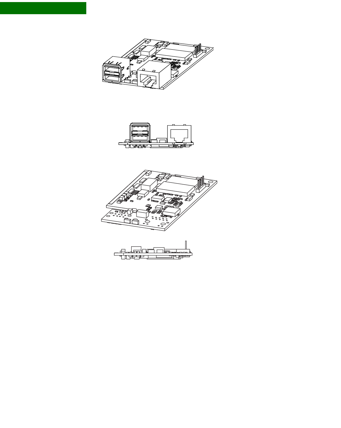
ConnectCore 9C configurations
The ConnectCore 9C module is available in these base configurations:
Fully populated. A fully populated module includes on-board Ethernet PHY,
Ethernet magnetics with RJ-45, a USB hub and Type A female connector.
With Ethernet but no USB Host. With this setup, Ethernet PHY or Ethernet
magnetics with RJ-45 are on the module. The module does not have an on-
board USB hub and Type A female connector, although USB Host and Device
signals are available on the edge connector.
No additional on-board connectors. With this setup, there is no Ethernet RJ-
45 with integrated magnetics on the module.
Note:
Modules without an on-board Ethernet connector provide the Ethernet
PHY signals through the SO-DIMM edge connector (see “Edge connector,
P3” on page 18).
Additional population options are available. For information, contact your local Digi
sales office or distributor.
Configuration
diagrams The diagrams in this section show configurations for the ConnectCore 9C module,
illustrated with top and edge views.
Standard configuration
With Ethernet
Without USB
ABOUT THE MODULES
ConnectCore 9C configurations
6ConnectCore 9c/Wi-9C Hardware Reference, Rev. B 01/2007
1
With Ethernet
With USB
Without Ethernet
Without USB

. . . . .
ABOUT THE MODULES
ConnectCoreWi-9C configurations
www.digiembedded.com 7
. . . . . . . . . . . . . . . . . . . . . . . . . . . . . . . . . . . . . . . . . . . . . . . . . . . . . . . . . . . . . . . . . . . . . . . . . . . . . . . . . .
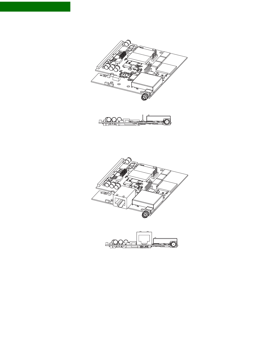
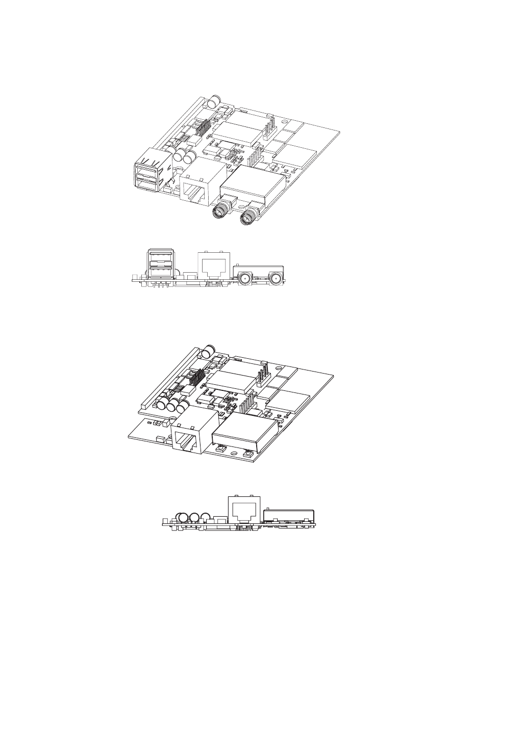
ConnectCoreWi-9C configurations
The ConnectCore Wi-9C module is available in these base configurations:
Fully populated, 2xRP-SMA. A fully populated module using RP-SMA includes
on-board Ethernet PHY, Ethernet magnetics with RJ-45, a USB hub and Type A
female connector, and two RP-SMA connectors.
With Ethernet, without USB, and with single RP-SMA. With this setup,
Ethernet PHY or Ethernet magnetics with RJ-45 are on the module. The module
does not have an on-board USB hub and Type A female connector, although USB
Host and Device signals are available on the edge connector. There is one RP-
SMA connector.
No additional on-board connectors, with single RP-SMA. With this setup,
there is no Ethernet RJ-45 with integrated magnetics on the module.There is
one RP-SMA connector.
Note:
Modules without an on-board Ethernet connector provide the Ethernet
PHY signals through the SO-DIMM edge connector (see “Edge connector,
P3” on page 18).
With Ethernet, without USB, and with 2xU.FL. With this setup, Ethernet PHY
or Ethernet magnetics with RJ-45 are on the module. The module does not
have an on-board USB hub and Type A female connector, although USB Host and
Device signals are available on the edge connector. There are two
U.FLconnectors.
Additional population options are available. For information, contact your local Digi
sales office or distributor.
Configuration
diagrams The diagrams in this section show configurations for the ConnectCore Wi-9C
module, illustrated with top and edge views.
ABOUT THE MODULES
ConnectCoreWi-9C configurations
8ConnectCore 9c/Wi-9C Hardware Reference, Rev. B 01/2007
1
Standard configuration
Without Ethernet
Without USB
With 1xRP-SMA connector
With Ethernet
Without USB
With 1xRP-SMA connector
. . . . .
ABOUT THE MODULES
ConnectCoreWi-9C configurations
www.digiembedded.com 9
Fully populated
With Ethernet
With USB
With 2xRP-SMA connectors
With Ethernet
Without USB
With 2xU.FL connectors

11
What’s on the Module?
CHAPTER 2
This chapter describes the ConnectCore 9C/Wi-9C modules. See Appendix A, ""
for the mechanical specifications and electrical characteristics of the modules.
. . . . . . . . . . . . . . . . . . . . . . . . . . . . . . . . . . . . . . . . . . . . . . . . . . . . . . . . . . . . . . . . . . . . . . . . . . . . . . . . . .
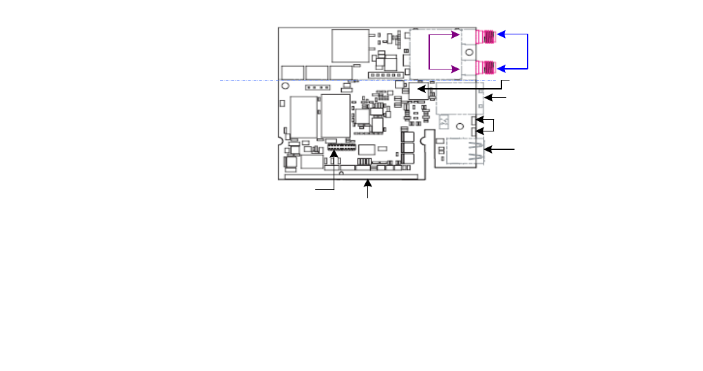
Module layout
The module design you use depends on whether you want to use the ConnectCore
Wi-9C wireless capabilities. The basic footprint for the ConnectCore 9C and
ConnectCore Wi-9C is the same; an extension of the footprint provides the active
components and antenna connectors for wireless functionality.
Note:
The ConnectCore Wi-9C module is populated with either one RP-SMA
connector, two RP-SMA connectors, or 2 U.FL connectors (see
“ConnectCoreWi-9C configurations” on page 7 for all module configuration
Module LEDs, CR1 & CR2
ConnectCore Wi-9C
(extended footprint)
Ethernet port
USB Host port, P6
PoE pass-through connector, P5
JTAG header connector, P2
SO-DIMM edge connector, P3
U.FL connector receptacles
P11
P9 RP-SMA connectors
P10
P8
ConnectCore 9C
(basic footprint)
WHAT’S ON THE MODULE?
Ethernet connector
12 ConnectCore 9c/Wi-9C Hardware Reference, Rev. B 01/2007
2
options). The U.FL connectors are located in the same positions as the RP-SMA
connectors, but do not extend past the edge of the module.
. . . . . . . . . . . . . . . . . . . . . . . . . . . . . . . . . . . . . . . . . . . . . . . . . . . . . . . . . . . . . . . . . . . . . . . . . . . . . . . . . .
Ethernet connector
The Ethernet connector is an 8-wire RJ-45 jack with integrated magnetics that
meets the ISO 8877 requirements for 10/100BASE-T. The connector provides both
Ethernet interface pins (in the upper portion) and two integrated LEDs (in the lower
portion).
Ethernet
connector pins There are eight Ethernet connector pins in the upper portion of the connector. Pin 1
is in the upper left corner of the connector, above the yellow LED. Pins 4, 5, 7, and
8 are used with Power-over-Ethernet (PoE) only (see “802.3af Power over Ethernet
(PoE) pass-through connector, P5” on page 13).
Ethernet LEDs The RJ-45 connector has two LEDs located near the outer lower corners of the
Ethernet port. These LEDs are controlled by the Ethernet PHY on the module, and
are not programmable.
Ethernet port
Pin Signal 802.3af End-Span (Mode A) 802.3af Mid-Span (Mode B) Description
1 TXD+ Negative VPort Transmit data +
2 TXD- Negative VPort Transmit data -
3RXD+ Positive VPort Receive data +
4EPWR+ Positive VPort Power from switch +
5EPWR+ Positive VPort Power from switch +
6RXD- Positive VPort Receive data -
7EPWR- Negative VPort Power from switch -
8EPWR- Negative VPort Power from switch -
. . . . .
WHAT’S ON THE MODULE?
802.3af Power over Ethernet (PoE) pass-through connector, P5
www.digiembedded.com 13
I
802.3af Power over Ethernet (PoE) pass-through
. . . . . . . . . . . . . . . . . . . . . . . . . . . . . . . . . . . . . . . . . . . . . . . . . . . . . . . . . . . . . . . . . . . . . . . . . . . . . . . . . .
connector, P5
The PoE pass-through connector, P5, mates with the P20 header on the development
board. This PoE pass-through feature passes PoE power connections from the
Ethernet signal cable to the user’s equipment through P5. The PoE feature provides
a power source for compliant “powered” equipment, and is nominally 48VDC with a
possible 30–57VDC 13 W maximum range.
Connector
description
PoE support If you are planning to add PoE support to your product, see the most recent revision
of the IEEE 802.3af specification available at http://www.ieee802.org/3/af/. The
document provides detailed information about the standard and its proper
implementation.
LED Description
Green Network link: On indicates an active network link; Off indicates that no network link is
present.
Yellow Network activity: Flashing when network traffic detected; Off when no network traffic
detected.
PoE pass-through
connector, P5
Pin Signal Description
1 TX_CT Ethernet transformer transmit CT
2 RJ45_7/8 Ethernet connector pins 7 and 8
3 RX_CT Ethernet transformer receive CT
4 RJ45_4/5 Ethernet connector pins 4 and 5
WHAT’S ON THE MODULE?
Module LEDs
14 ConnectCore 9c/Wi-9C Hardware Reference, Rev. B 01/2007
2
. . . . . . . . . . . . . . . . . . . . . . . . . . . . . . . . . . . . . . . . . . . . . . . . . . . . . . . . . . . . . . . . . . . . . . . . . . . . . . . . . .
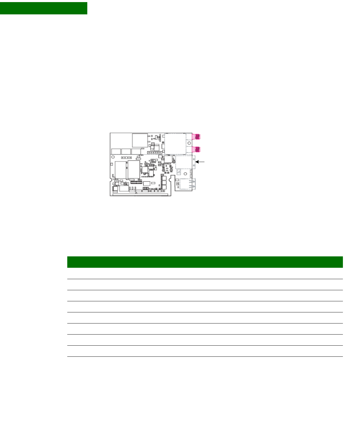
Module LEDs
By default, the ConnectCore 9C/Wi-9C modules use the CR1 and CR2 LEDs as
described:
ConnectCore Wi-9C module: To indicate WLAN-related information, such as
association status and network activity.
ConnectCore 9C and Wi-9C modules: CR1 will flash a repeating blink pattern
in a major system failure; for example, a processor exception or Power on Self
Test failure.
The ConnectCore Wi-9C LED assignments can be reassigned; that is, you can use
different GPIOs to drive CR1/CR2 LEDs.
Description
ConnectCore
Wi-9C default use
Module LEDs,
CR1 & CR2
ID Connects to Default Description
CR1 GPIO67 Off Setting to output logic “0” turns on the LED.
CR2 GPIO66 Off Setting to output logic “0” turns on the LED.
ID Color LED Blink pattern Status / Activity
CR1 Green Link integrity On The unit is associated to an access point
(infrastructure mode)
Slow The unit is in ad-hoc mode
Quick The unit is scanning for a network
CR2 Yellow Network activity Blinking Network traffic is received or transmitted
Off Network is idle
Note: The network activity LED is used for diagnostic purposes during boot-up.
. . . . .
WHAT’S ON THE MODULE?
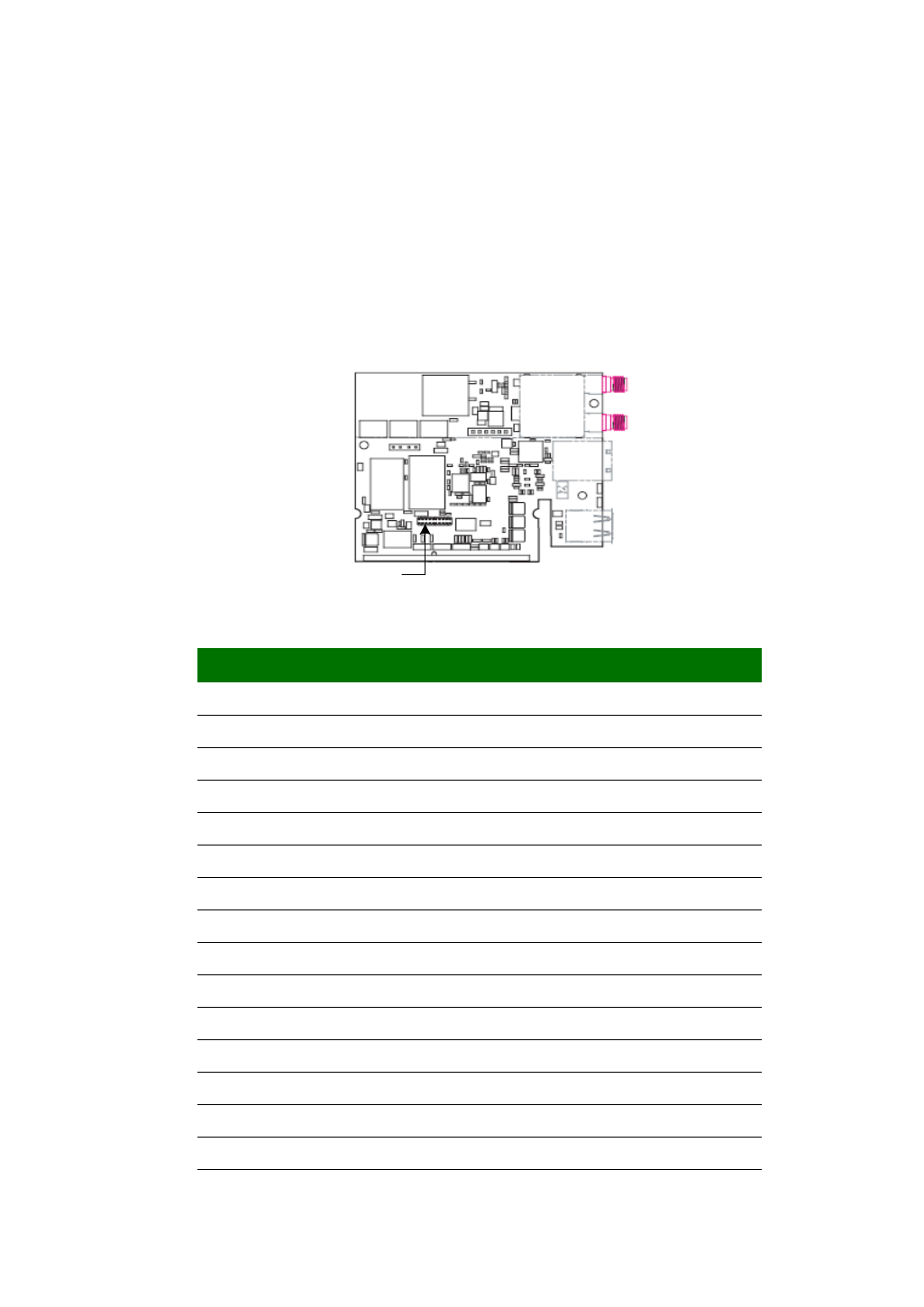
JTAG 20-pin header connector, P2
www.digiembedded.com 15
. . . . . . . . . . . . . . . . . . . . . . . . . . . . . . . . . . . . . . . . . . . . . . . . . . . . . . . . . . . . . . . . . . . . . . . . . . . . . . . . . .
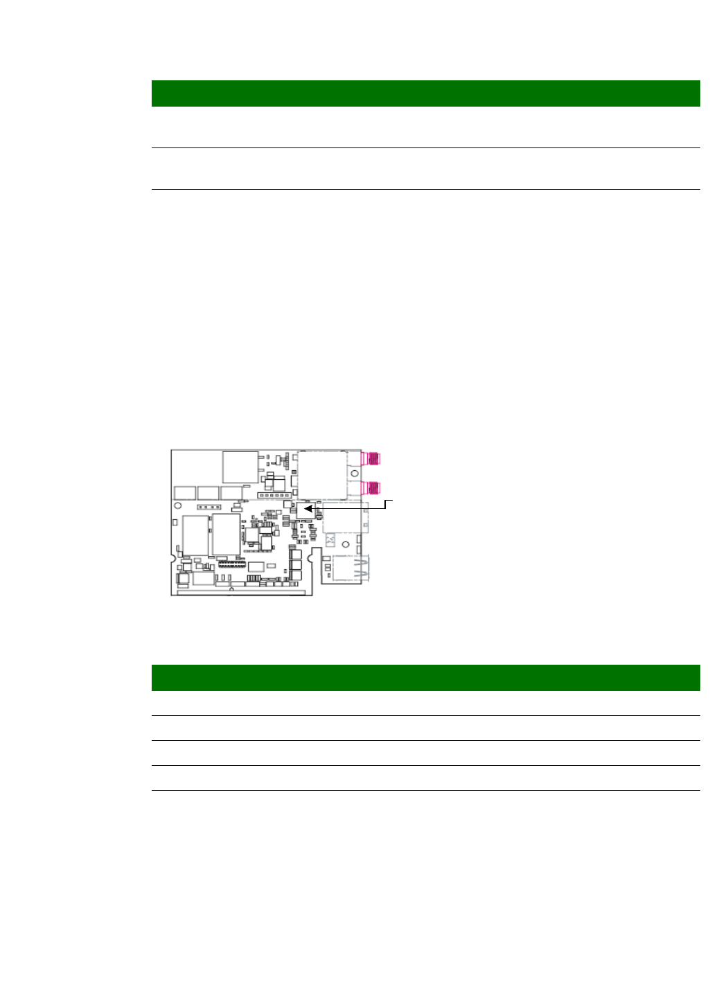
JTAG 20-pin header connector, P2
The JTAG connector is a standard, male, ARM 20-pin pinout in a miniature
connector, with a 50-mil pitch. A JTAG adapter, which ships with each Jump Start
kit, expands the JTAG connector to a 100 mil pitch. Use the included JTAG adapter
to connect the debugger.
The JTAG connector on the module is keyed, as are the two connectors on the JTAG
adapter, which means there is only one way to attach ribbon cables to the module
and JTAG adapter. For details, see “JTAG adapter assembly” on page 16.
Pin assignment
JTAG header connector, P2
Pin Signal Description
1 3.3V ARM9 I/O supply
2 3.3V ARM9 I/O supply
3 TRST# Test mode reset
4 GND Ground
5 TDI Test data in
6 GND Ground
7 TMS Test mode select
8 GND Ground
9TCK Test clock
10 GND Ground
11 RTCK Returned test clock (ARM core only)
12 GND Ground
13 TDO Test data out
14 GND Ground
15 DBSRST# System reset
16 GND Ground
WHAT’S ON THE MODULE?
JTAG adapter assembly
16 ConnectCore 9c/Wi-9C Hardware Reference, Rev. B 01/2007
2
. . . . . . . . . . . . . . . . . . . . . . . . . . . . . . . . . . . . . . . . . . . . . . . . . . . . . . . . . . . . . . . . . . . . . . . . . . . . . . . . . .
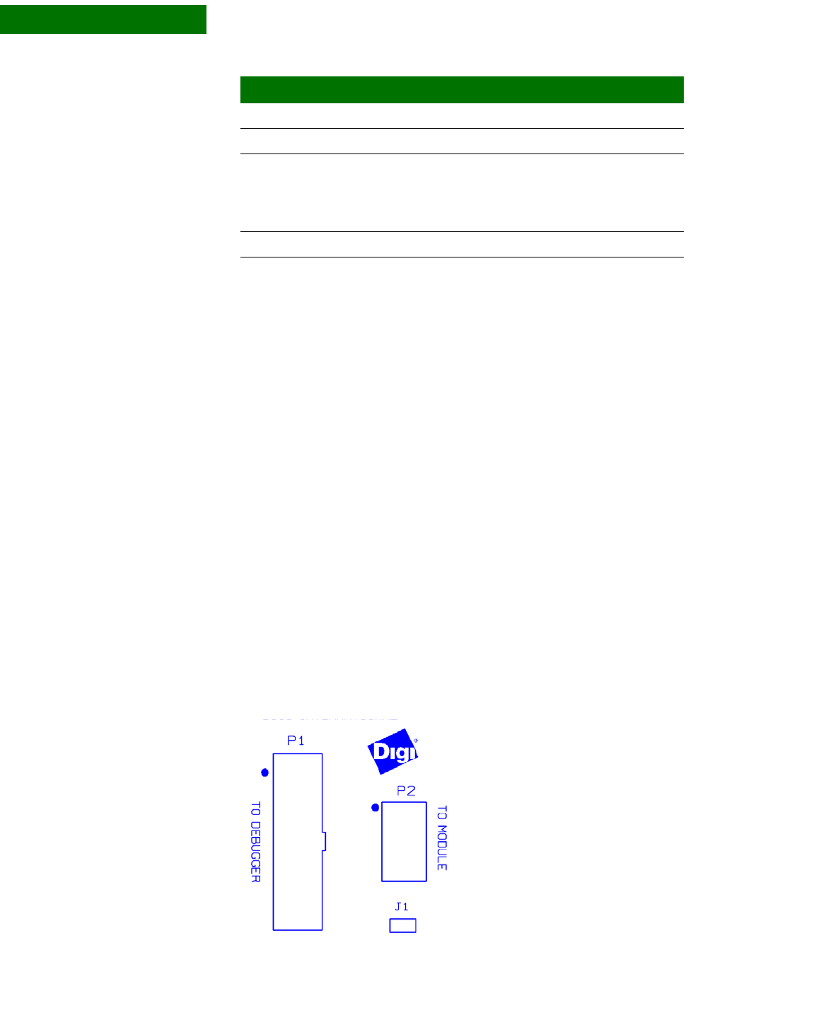
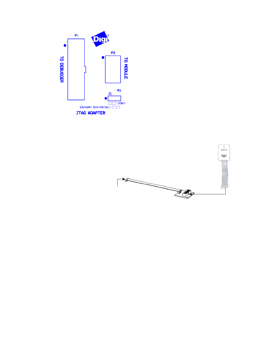
JTAG adapter assembly
Use the JTAG adapter assembly, shipped with the ConnectCore 9C/Wi-9C Jump Start
Kit, to attach your debugger to the module. The JTAG adapter assembly consists of
the Digi JTAG Link USB debugger with a ribbon cable attached and the JTAG adapter
with a ribbon cable attached. The Jump Start Kit also includes a USB cable.
The two connectors on the JTAG adapter are keyed, as is the JTAG connector
header (P2) on the module. Keyed connectors eliminate cable attachment errors by
ensuring that there is only one way to mate the connectors.
JTAG adapter The JTAG adapter has two 20-pin connectors, P1 and P2.
P1 is a keyed male connector into which you attach the debugger’s ribbon
cable.
P2 is a keyed male connector into which you attach the ribbon cable that plugs
into the module.
J1 is a jumper that determines the mode in which the module operates: debug
or boundary scan. Depending on the JTAG adaptor you are using, J1 has either
two pins or three pins.
This drawing shows the JTAG adapter with a 2-
pin J1 header.
For debug mode — Do not plug a jumper onto J1.
For boundary scan mode — Plug a jumper onto
J1.
17 N/A N/A
18 GND Ground
19 BISTEN# ARM9 mode select:
Debug = Pull high: 220 ohms to pin 2 (3.3V)
Boundary scan / normal = Pull low: 220 ohms
to pin 20 (GND)
20 GND Ground
Pin Signal Description
. . . . .
WHAT’S ON THE MODULE?
JTAG adapter assembly
www.digiembedded.com 17
This drawing shows the JTAG adapter with a 3-
pin J1 header. The pin positions for debug and
boundary scan are shown in the lower right of
the drawing:
For debug mode — Plug a jumper on pins 1 and
2.
For boundary scan mode (the default) — Plug a
jumper on pins 2 and 3.
Assembly 1Plug the
debugger
ribbon cable
into the
connector
labeled P1 on
the JTAG
adapter.
2Plug the
adapter
ribbon cable
(attached to
P2 on the
adapter) into
the P2
connector on the module.
20-pin female
connector
Digi JTAG Link USB
debugger
Ribbon cable to attach
adapter to module
Step 2: Plug this end
of the cable into the
P2 connector on the
module. Step 1: Plug the
debugger ribbon cable
into the connector
labeled P1 on the JTAG
adapter.
P1
P2
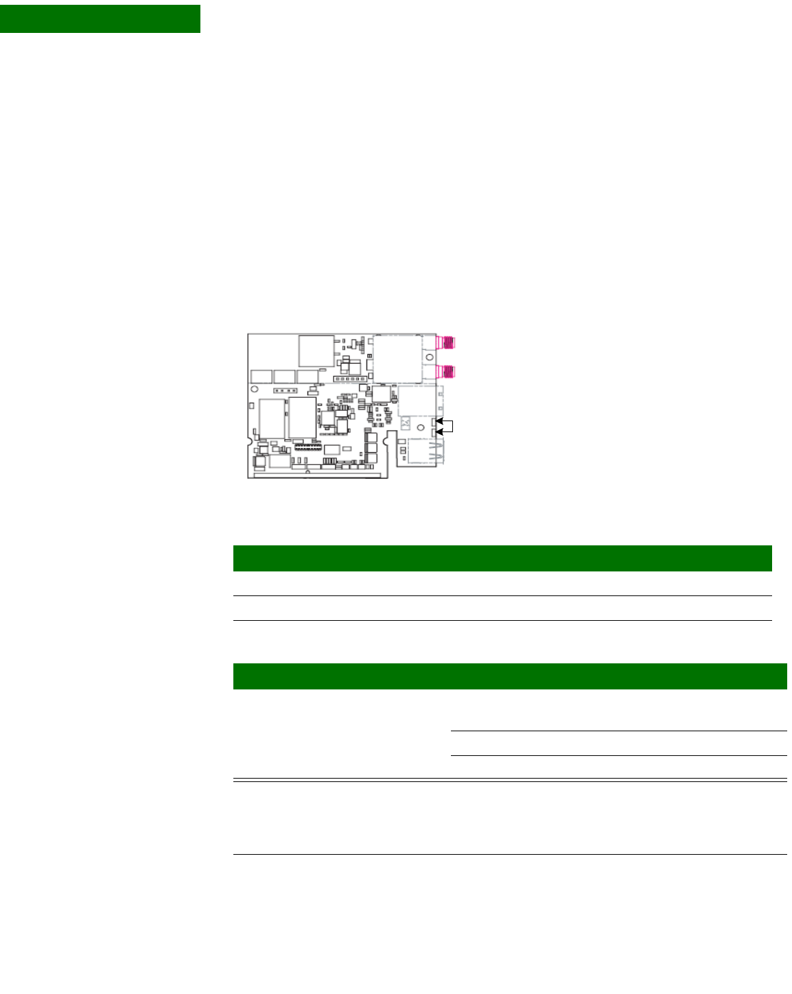
WHAT’S ON THE MODULE?
USB Host connector, P6
18 ConnectCore 9c/Wi-9C Hardware Reference, Rev. B 01/2007
2
. . . . . . . . . . . . . . . . . . . . . . . . . . . . . . . . . . . . . . . . . . . . . . . . . . . . . . . . . . . . . . . . . . . . . . . . . . . . . . . . . .
USB Host connector, P6
When populated, the USB Host connector is on the same side of the module as the
Ethernet connector, separated from the Ethernet connector by CR1 and CR2.
See “USB interface” on page 68 for information about the USB interface.
. . . . . . . . . . . . . . . . . . . . . . . . . . . . . . . . . . . . . . . . . . . . . . . . . . . . . . . . . . . . . . . . . . . . . . . . . . . . . . . . . .
Edge connector, P3
The edge connector is a 144-pin SO-DIMM connector located on the short edge of
the module. P3 mates with P15 (also a 144-position SO-DIMM connector) on the
development board or an SO-DIMM connector on your design.
Note:
The clearance underneath the module and development board should be
2.54mm (0.10”).
Pin assignment The next tables show information for all pins on the edge connector, in DIMM pin
order. For additional SO-DIMM pin characteristics, see "Module / SO-DIMM signal
characteristics," beginning on page 70.
Some signals are multiplexed to two different GPIO pins, to maximize the
number of possible applications. The primary/duplicate signals are noted in
USB Host port, P6
SO-DIMM edge connector, P3

. . . . .
WHAT’S ON THE MODULE?
Edge connector, P3
www.digiembedded.com 19
the Notes column in the table. Using the primary GPIO pin and the duplicate
pin for the same function is not recommended.
Note: Functions in parentheses are duplicates; for example, pin 63 has two
entries in the LCD column: CLD6 and (CLD10). CLD10 is a duplicate signal for
pin 63; the Notes column identifies the primary function for that signal.
A # next to a signal indicates that this signal is active low.
A bold value in the System / Other / Bootstrap column indicates the bootstrap
signal.
Pin assignment by
SO-DIMM pin
number
Dimm
Pin Signal BootStrap
(BS) /
System /
Other
UART SPI I2C USB LCD IEEE
1284 PWM /
Timer
/ IRQ
Notes
1GND Common GND return
2GND Common GND return
3 +3.3V Power to module
4 +3.3V Power to module
5 +3.3V Power to module
6 +3.3V Power to module
7WAKEUP#
PWRDWN# System Wi-9C: WAKEUP# / Reserved
CC9C: PWRDWN# / Reserved
8 BUFFENR# System Use to isolate bootstrap GPIOs from
external loading
9 DATA_0 Data bus Wi-9C only
CC9C: Reserved
10 DATA_1 Data bus Wi-9C only
CC9C: Reserved
11 DATA_2 Data bus Wi-9C only
CC9C: Reserved
12 DATA_3 Data bus Wi-9C only
CC9C: Reserved
13 DATA_4 Data bus Wi-9C only
CC9C: Reserved
14 DATA_5 Data bus Wi-9C only
CC9C: Reserved
15 DATA_6 Data bus Wi-9C only
CC9C: Reserved
16 DATA_7 Data bus Wi-9C only
CC9C: Reserved
17 ADDRESS_0 Address bus Wi-9C only
CC9C: Reserved
18 ADDRESS_1 Address bus Wi-9C only
CC9C: Reserved

WHAT’S ON THE MODULE?
Edge connector, P3
20 ConnectCore 9c/Wi-9C Hardware Reference, Rev. B 01/2007
2
19 GND Common GND return
20 GND Common GND return
21 ADDRESS_2 Address bus Wi-9C only
CC9C: Reserved
22 MFGI_
GPIO[72] Reserved
23 ADDRESS_3 Address bus Wi-9C only
CC9C: Reserved
24 GPIO[71] iic_sda GPIO[71]: Output drive 8mA
iic_sda: Primary on GPIO[35]
25 ADDRESS_4 Address bus Wi-9C only
CC9C: Reserved
26 GPIO[70] iic_scl GPIO[70]: Output drive 8mA
iic_scl: Primary on GPIO[34]
27 ADDRESS_5 Address bus Wi-9C only
CC9C: Reserved
28 GPIO[69] IRQ1 GPIO[69]: Output drive 8mA
IRQ1: Primary on GPIO[07]
Add 10-15K pullup if not used
29 GND Common GND return
30 GND Common GND return
31 GPIO[27] DCD_D ENBL_D CLD3 TIMER4
32 No connect
33 GPIO[26] RI_D CLK_D CLD2 TIMER3
34 GPIO[67] CR1: Green user LED
Output drive 8mA
MFGO_CR1
35 GPIO[25] DSR_D CLD1
36 GPIO[66] CR2: Yellow user LED
Output drive 8mA
37 GPIO[24] BS:
CS1_MSB DTR_D CLD0
38 GPIO[23] DCD_C ENBL_C CLLE
39 GND Common GND return
40 GND Common GND return
41 GPIO[47] CTS_D RXD- PINIT# RXD-: Only used for unidirectional
PHY
42 GPIO[22] RI_C CLK_C CLAC
43 GPIO[46] RTS_D RXD+ PAFD# RXD+: Only used for unidirectional
PHY
44 GPIO[21] DSR_C CLFP
VSYNC
45 GPIO[45] RXD_D DIN_D RCV PSTB#
Dimm
Pin Signal BootStrap
(BS) /
System /
Other
UART SPI I2C USB LCD IEEE
1284 PWM /
Timer
/ IRQ
Notes

. . . . .
WHAT’S ON THE MODULE?
Edge connector, P3
www.digiembedded.com 21
46 GPIO[20] BS: CS1_LSB DTR_C CLCP/LDC
CLKO GPIO[20]: Output drive 8mA
47 GPIO[44] BS: Endian
Pull down for
Big Endian
TXD_D DOUT_D OE PSELO
48 GPIO[43] CTS_C DATA- PDIR Add 10-15K pullup if not used
49 GND Common GND return
50 GND Common GND return
51 GPIO[38] CLD14 PD7 PWM2 PWM2: Duplicate on GPIO[13]
52 GPIO[42] RTS_C DATA+ Add 10-15K pullup if not used
53 GPIO[36] CLD12 PD5 PWM0 PWM0: Duplicate on GPIO[10]
54 GPIO[41] RXD_C DIN_C CLD17
55 GPIO[34] SCL CLD10 PD3 SCL: Duplicate on GPIO[70]
CLD10: Duplicate on GPIO[30]
56 GPIO[40] TXD_C DOUT_C CLD16 IRQ3 IRQ3: Duplicate on GPIO[18]
57 GPIO[32] CLD8 PD1 IRQ2 CLD8: Duplicate on GPIO[28]
IRQ2: Duplicate on GPIO[11]
58 GPIO[39] CLD15 PD8 PWM3 PWM3: Duplicate on GPIO[14]
59 GND Common GND return
60 GND Common GND return
61 GND Common GND return
62 GND Common GND return
63 GPIO[30] CLD6
(CLD10) TIMER6 CLD10: Primary on GPIO[34]
64 GPIO[37] CLD13 PD6 PWM1 PWM1: Duplicate on GPIO[12]
65 GPIO[28] CLD4
(CLD8) IRQ1 CLD8: Primary on GPIO[32]
IRQ1: Primary on GPIO[07]
66 GPIO[35] SDA CLD11 PD4 SDA: Duplicate on GPIO[71]
CLD11: Primary on GPIO[13]
67 GPIO[15] DCD_A ENBL A LCDCLKI TIMER2
68 GPIO[33] CLD9 PD2 CLD9: Duplicate on GPIO[29]
69 GPIO[14] RI_A CLK A PWM3
TIMER1 PWM3: Primary on GPIO[39]
TIMER1: Duplicate on GPIO[00]
70 GPIO[31] CLD7
(CLD11) TIMER7 CLD11: Primary on GPIO[35]
TIMER7: Duplicate on GPIO[06]
71 GND Common GND return
72 GND Common GND return
73 GPIO[13] DSR_A PWM2
IRQ0 PWM2: Primary on GPIO[38]
IRQ0: Primary on GPIO[01]
74 GPIO[29] CLD5
(CLD9) TIMER5 CLD9: Primary on GPIO[33]
75 GPIO[12] BS: ND3 DTR_A PWM1 PWM1: Primary on GPIO[37]
Dimm
Pin Signal BootStrap
(BS) /
System /
Other
UART SPI I2C USB LCD IEEE
1284 PWM /
Timer
/ IRQ
Notes

WHAT’S ON THE MODULE?
Edge connector, P3
22 ConnectCore 9c/Wi-9C Hardware Reference, Rev. B 01/2007
2
76 GPIO[07] DCD_B ENBL_B IRQ1 IRQ1: Duplicate on GPIO[28] and
GPIO[65]
77 GPIO[11] CTS_A TIMER0
IRQ2 TIMER0: Primary on GPIO[02]
IRQ2: Primary on GPIO[32]
78 GPIO[06] RI_B CLK_B PFAULT# TIMER7 PFAULT: Primary on GPIO[16]
TIMER7: Primary on GPIO[31]
79 GPIO[10] BS: ND2 RTS_A PWM0 PWM0: Primary on GPIO[36]
80 GPIO[05] DSR_B PERR
81 GND Common GND return
82 GND Common GND return
83 GPIO[09] RXD_A DIN_A
84 GPIO[04] BS: ND0 DTR_B PBUSY
85 GPIO[08] BS: ND1 TXD_A DOUT_A
86 GPIO[03] CTS_B PACK#
87 GPIO[19] BS:
PLL_BYP CLLP/
HSYNC PLL_BYP: Reserved. Do not pull
down
88 GPIO[02] BS: FS1 RTS_B TIMER0 TIMER0: Duplicate on GPIO[11]
89 GPIO[18] CLPOWER IRQ3 IRQ3: Primary on GPIO[40]
90 GPIO[01] RXD_B DIN_B IRQ0 IRQ0: Duplicate on GPIO[13] and
GPIOP[68]
91 OE# Output enable Wi-9C only
CC9C: Reserved
92 GPIO[00] BS: FS0 TXD_B DOUT_B TIMER1 TIMER1: Primary on GPIO[14]
93 GND Common GND return
94 GND Common GND return
95 WE# Write enable Wi-9C only
CC9C: Reserved
96 GPIO[49] BS: CS_POL SPD PLH
97 CS# Chip select Wi-9C only
CC9C: Reserved
98 GPIO[48] SUSP PSELI
99 TXB+R Ethernet Reserved
100 TXA+R Ethernet Reserved
101 GND Common GND return
102 GND Common GND return
103 TXB-R Ethernet Reserved
104 TXA-R Ethernet Reserved
105 RST# System Hardware reset (input; active LOW;
minimum pulse width 10uS)
106 ACT_LED# Ethernet Reserved
107 BOOTMUXR# System Reserved
Dimm
Pin Signal BootStrap
(BS) /
System /
Other
UART SPI I2C USB LCD IEEE
1284 PWM /
Timer
/ IRQ
Notes

. . . . .
WHAT’S ON THE MODULE?
Edge connector, P3
www.digiembedded.com 23
108 LNK_LED Ethernet Wi-9C only
CC9C: Reserved
109 GPIO[16] OVRH# PFAULT# PWM0 OVRH#: USB overcurrent input.
Available as GPIO on modules with
USB hub or Ethernet only. Not
available as GPIO if an external Host
USB port is implemented using
DM1 and DP1.
PFAULT#: Primary on GPIO[06]
PWM0: Duplicate on GPIO[10]
110 ADDRESS_6 Address bus Wi-9C only
CC9C: Reserved
111 GPIO[17] ND4 PONH# PONH#: USB power on output.
Available as GPIO on modules with
USB hub or Ethernet only. Not
available as GPIO if an external Host
USB port is implemented using
DM1 and DP1.
112 ADDRESS_7 Address bus Wi-9C only
CC9C: Reserved
113 OVR3# USB port 3 overcurrent
Reserved for future use; no connect
114 OVR4# USB port 4 overcurrent
Reserved for future use; no connect
115 PON3# USB port 3 power-on
Reserved for future use; no connect
116 PON4# USB port 4 power-on
Reserved for future use; no connect
117 OVR1# USB port 1 overcurrent
Reserved for future use; no connect
118 OVR2# USB port 2 overcurrent
Reserved for future use; no connect
119 PON1# USB port 1 power-on
Reserved for future use; no connect
120 PON2# USB port 2 power-on
Reserved for future use; no connect
121 GND Common GND return
122 GND Common GND return
123 DM4 USB port 4 data (-)
Reserved for future use; no connect
124 DP4 USB port 4 data (+)
Reserved for future use; no connect
125 GND Common GND return
126 GND Common GND return
127 DM3 USB port 3 data (-)
Reserved for future use; no connect
128 DP3 USB port 3 data (+)
Reserved for future use; no connect
129 GND Common GND return
Dimm
Pin Signal BootStrap
(BS) /
System /
Other
UART SPI I2C USB LCD IEEE
1284 PWM /
Timer
/ IRQ
Notes

WHAT’S ON THE MODULE?
Edge connector, P3
24 ConnectCore 9c/Wi-9C Hardware Reference, Rev. B 01/2007
2
Pin assignment by
GPIO
130 GND Common GND return
131 DM2 USB port 2 data (-)
Reserved for future use; no connect
132 DP2 USB port 2 data (+)
Reserved for future use; no connect
133 GND Common GND return
134 GND Common GND return
135 DM1 USB port 1 data (-)
Reserved for future use; no connect
136 DP1 USB port 1 data (+)
Reserved for future use; no connect
137 GND Common GND return
138 GND Common GND return
139 +5V Power to USB, if used (Used only
with a module with on-board USB)
140 +5V Power to USB, if used (Used only
with a module with on-board USB)
141 +5V Power to USB, if used (Used only
with a module with on-board USB)
142 +5V Power to USB, if used (Used only
with a module with on-board USB)
143 GND Common GND return
144 GND Common GND return
Dimm
Pin Signal BootStrap
(BS) /
System /
Other
UART SPI I2C USB LCD IEEE
1284 PWM /
Timer
/ IRQ
Notes
Signal SO-
DIMM BootStrap
(BS /
System /
Other
UART SPI I2C USB LCD IEEE
1284 PWM /
Timer
/ IRQ
Notes
GPIO[00] 92 BS: FS0 TXD_B DOUT_B TIMER1 TIMER1: Primary on GPIO[14]
GPIO[01] 90 RXD_B DIN_B IRQ0 IRQ0: Duplicate on GPIO[13] and
GPIOP[68]
GPIO[02] 88 BS: FS1 RTS_B TIMER0 TIMER0: Duplicate on GPIO[11]
GPIO[03] 86 CTS_B PACK#
GPIO[04] 84 BS: ND0 DTR_B PBUSY
GPIO[05] 80 DSR_B PERR
GPIO[06] 78 RI_B CLK_B PFAULT# TIMER7 PFAULT: Primary on GPIO[16]
TIMER7: Primary on GPIO[31]
GPIO[07] 76 DCD_B ENBL_B IRQ1 IRQ1: Duplicate on GPIO[28] and
GPIO[65]
GPIO[08] 85 BS: ND1 TXD_A DOUT_A
GPIO[09] 83 RXD_A DIN_A

. . . . .
WHAT’S ON THE MODULE?
Edge connector, P3
www.digiembedded.com 25
GPIO[10] 79 BS: ND2 RTS_A PWM0 PWM0: Primary on GPIO[36]
GPIO[11] 77 CTS_A TIMER0
IRQ2 TIMER0: Primary on GPIO[02]
IRQ2: Primary on GPIO[32]
GPIO[12] 75 BS: ND3 DTR_A PWM1 PWM1: Primary on GPIO[37]
GPIO[13] 73 DSR_A PWM2
IRQ0 PWM2: Primary on GPIO[38]
IRQ0: Primary on GPIO[01]
GPIO[14] 69 RI_A CLK_A PWM3
TIMER1 PWM3: Primary on GPIO[39]
TIMER1: Duplicate on GPIO[00]
GPIO[15] 67 DCD_A ENBL_A LCDCLKI TIMER2
GPIO[16] 109 OVRH# PFAULT# PWM0 OVRH#: USB overcurrent input.
Available as GPIO on modules with
USB hub or Ethernet only, and not
required for external USB Host
support.
PFAUL#T: Primary on GPIO[06]
PWM0: Duplicate on GPIO[10]
GPIO[17] 111 ND4 PONH# PONH#: USB power on output.
Available as GPIO on modules with
USB hub or Ethernet only, and not
required for external USB Host
support.
GPIO[18] 89 CLPOWER IRQ3 IRQ3: Primary on GPIO[40]
GPIO[19] 87 BS:
PLL_BYP CLLP/HSY
NC PLL_BYP: Reserved. Do not pull
down
GPIO[20] 46 BS: CS1_LSB DTR_C CLCP/LDC
CLKO GPIO[20]: Output drive 8mA
GPIO[21] 44 DSR_C CLFP
VSYNC
GPIO[22] 42 RI_C CLK_C CLAC
GPIO[23] 38 DCD_C ENBL_C CLLE
GPIO[24] 37 BS:
CS1_MSB DTR_D CLD0
GPIO[25] 35 DSR_D CLD1
GPIO[26] 33 RI_D CLK_D CLD2 TIMER3
GPIO[27] 31 DCD_D ENBL_D CLD3 TIMER4
GPIO[28] 65 CLD4
(CLD8) IRQ1 CLD8: Primary on GPIO[32]
IRQ1: Primary on GPIO[07]
GPIO[29] 74 CLD5
(CLD9) TIMER5 CLD9: Primary on GPIO[33]
GPIO[30] 63 CLD6
(CLD10) TIMER6 CLD10: Primary on GPIO[34]
GPIO[31] 70 CLD7
(CLD11) TIMER7 CLD11: Primary on GPIO[35]
TIMER7: Duplicate on GPIO[06]
GPIO[32] 57 CLD8 PD1 IRQ2 CLD8: Duplicate on GPIO[28]
IRQ2: Duplicate on GPIO[11]
GPIO[33] 68 CLD9 PD2 CLD9: Duplicate on GPIO[29]
Signal SO-
DIMM BootStrap
(BS /
System /
Other
UART SPI I2C USB LCD IEEE
1284 PWM /
Timer
/ IRQ
Notes

WHAT’S ON THE MODULE?
Antenna connectors: RP/SMA and U.FL (ConnectCore Wi-9C only)
26 ConnectCore 9c/Wi-9C Hardware Reference, Rev. B 01/2007
2
Antenna connectors: RP/SMA and U.FL (ConnectCore Wi-9C
. . . . . . . . . . . . . . . . . . . . . . . . . . . . . . . . . . . . . . . . . . . . . . . . . . . . . . . . . . . . . . . . . . . . . . . . . . . . . . . . . .
only)
The ConnectCore Wi-9C supports two types of antenna connectors: RP-SMA and
U.FL. The standard connector population option is 1 RP-SMA connector. Dual
diversity operation and custom connector populations are available.
GPIO[35] 66 SDA CLD11 PD4 SDA: Duplicate on GPIO[71]
CLD11: Primary on GPIO[13]
GPIO[36] 53 CLD12 PD5 PWM0 PWM0: Duplicate on GPIO[10]
GPIO[37] 64 CLD13 PD6 PWM1 PWM1: Duplicate on GPIO[12]
GPIO[38] 51 CLD14 PD7 PWM2 PWM2: Duplicate on GPIO[13]
GPIO[39] 58 CLD15 PD8 PWM3 PWM3: Duplicate on GPIO[14]
GPIO[40] 56 TXD_C DOUT_C CLD16 IRQ3 IRQ3: Duplicate on GPIO[18]
GPIO[41] 54 RXD_C DIN_C CLD17
GPIO[42] 52 RTS_C DATA+ Add 10-15K pullup if not used
GPIO[43] 48 CTS_C DATA- PDIR Add 10-15K pullup if not used
GPIO[44] 47 BS: Endian
Pull down for
Big Endian
TXD_D DOUT_D OE PSELO
GPIO[45] 45 RXD_D DIN_D RCV PSTB#
GPIO[46] 43 RTS_D RXD+ PAFD# RXD+: Only used for unidirectional
PHY
GPIO[47] 41 CTS_D RXD- PINIT# RXD-: Only used for unidirectional
PHY
GPIO[48] 98 SUSP PSELI
GPIO[49] 96 BS: CS_POL SPD PLH
GPIO[66] 36 CR2: Yellow user LED
Output drive 8mA
GPIO[67] 34 CR1: Green user LED
Output drive 8mA
MFGO_CR1
GPIO[68] NC No connect
GPIO[69] 28 IRQ1 GPIO[69]: Output drive 8mA
IRQ1: Primary on GPIO[07]
Add 10-15K pullup if not used
GPIO[70] 26 iic_scl GPIO[70]: Output drive 8mA
iic_scl: Primary on GPIO[34]
GPIO[71] 24 iic_sda GPIO[71]: Output drive 8mA
iic_sda: Primary on GPIO[35]
MFGI_
GPIO[72] 22 Reserved
Signal SO-
DIMM BootStrap
(BS /
System /
Other
UART SPI I2C USB LCD IEEE
1284 PWM /
Timer
/ IRQ
Notes
. . . . .
WHAT’S ON THE MODULE?
Antenna connectors: RP/SMA and U.FL (ConnectCore Wi-9C only)
www.digiembedded.com 27
For antenna specifications, see "Antenna information," beginning on page 77.
RP-SMA
connectors, P10
and P8
The antenna is connected to the module via a reverse polarity SMA connector (sub-
miniature size A). The antenna fits on the module only one way, to ensure proper
connection.
Caution:
Be sure that your antenna choice complies with the regulatory
requirements of your region. In North America, for example, you can
operate only with antennas approved by Digi International, Inc., or
antennas matching the specifications of the Digi-approved antennas.
Primary RP-SMA antenna, P10
P10 is the primary RP-SMA
antenna, for both receive and
transmit. This is the
connector/antenna provided with
the standard RP-SMA module
configuration.
Secondary RP-SMA antenna, P8
P8 is the secondary RP-SMA
antenna, used for receive only.
This connector/antenna is
provided only when you select the
two-RP-SMA population option.
U.FL connectors,
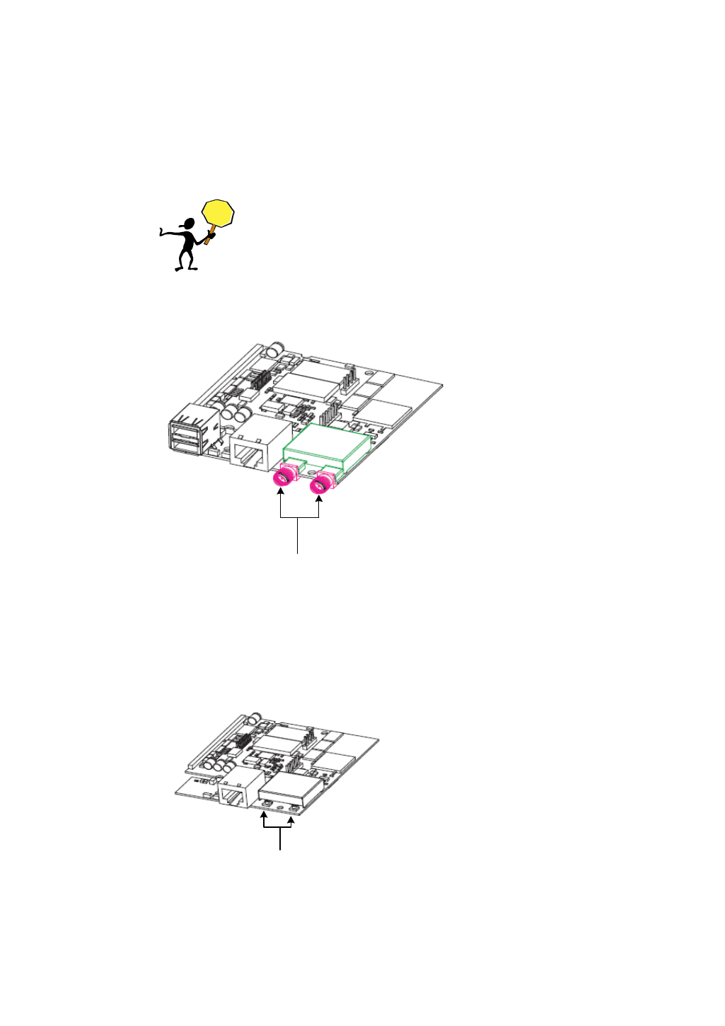
P11 and P9 Both U.FL connectors are provided on the module when you select the U.FL
population option.
P11 is the primary U.FL antenna, for both
receive and transmit. P9 is the secondary
U.FL antenna, used for receive only.
RP-SMA connectors
P10
P8
U.FL connectors
P11
P9

WHAT’S ON THE MODULE?
Antenna connectors: RP/SMA and U.FL (ConnectCore Wi-9C only)
28 ConnectCore 9c/Wi-9C Hardware Reference, Rev. B 01/2007
2

29
About the Development Board
CHAPTER 3
This chapter provides information for configuring the ConnectCore 9C/Wi-9C
development board, and details the development board’s default and optional
configuration states. The development board serves as a carrier board platform for
product evaluation and design. The board is also available as a separate accessory
item for quick prototyping purposes.
For more detailed information on the development board, see the documentation
available on your Jump Start Kit CD.
Features The ConnectCore 9C/Wi-9C development board supports these features:
Four 921kbps serial ports
–Serial port A: EIA-232/422/485 switch-selectable (DB-9)
–Serial port B: EIA-232 (DB-9)
–Serial port C: TTL-level
–Serial port D: TTL-level
SPI and I2C interface headers
Eight digital GPIOs
Two user LEDs and pushbuttons
VGA interface
LCD panel connector
Application-specific expansion connectors
Through-hole prototyping area
+3.3V, +5V, +12V, -12V, and GND test points
ABOUT THE DEVELOPMENT BOARD
Basic description
30 ConnectCore 9c/Wi-9C Hardware Reference, Rev. B 01/2007
3
Current measurement option
Power on/off switch
9-30VDC power input
Board and module mounting holes
. . . . . . . . . . . . . . . . . . . . . . . . . . . . . . . . . . . . . . . . . . . . . . . . . . . . . . . . . . . . . . . . . . . . . . . . . . . . . . . . . .
Basic description
The development board contains connectors, switches, and LEDs that you use when
integrating the ConnectCore 9C or ConnectCore Wi-9C module into your design. The
board also provides test points; see “Test points” on page 57 for more information.
I2C header connector, P8
SPI header connector, P7 LCD application header, P18
PoE
connector,
P20
SO-DIMM connector, P15 Hardware
reset, SW6
External
LCD clock,
G1
Platform application board header, P17
Digital I/O,
P19
Peripheral application board header, P16
Serial port D, P11
Through-hole signal rail, P3
Through-hole
prototyping
(wrap-field)
area, P4
Serial port C, P10
User LEDs,
CR6 & CR7
User
pushbuttons,
SW3 & SW4
Serial port
B, P9
Serial port B
switch, SW2
Serial status LEDs
USB Device application header, P32
A
B
Serial port
A, P13
Serial port A
switch, SW1
VGA
connector,
P6
VGA (enable)
switch, SW7
Power
jack, P12
Power
LEDs PoE sockets, P30 & P31
Current
measurement
option, CMO
R69
R78
Power switch, SW5
. . . . .
ABOUT THE DEVELOPMENT BOARD
Switches and buttons
www.digiembedded.com 31
. . . . . . . . . . . . . . . . . . . . . . . . . . . . . . . . . . . . . . . . . . . . . . . . . . . . . . . . . . . . . . . . . . . . . . . . . . . . . . . . . .
Switches and buttons
Serial Port A
switch, SW1 The Serial Port A switch is a 4-position DIP switch. Use this switch to set the signal
modes for serial port A, EIA-232/422/485.
Hardware
reset, SW6
User
pushbuttons,
SW3 & SW4
Serial port B
switch, SW2
Serial port A
switch, SW1
VGA (enable)
switch, SW7
Power switch, SW5
Position Description Default
position
1 Determines whether the interface is configured for EIA-232 or
EIA-485:
ON — EIA-232 interface mode
OFF — EIA-485 interface mode
ON
2 Enables/disables EIA-232 auto power down:
ON — Not supported
OFF — Disabled
OFF

ABOUT THE DEVELOPMENT BOARD
Switches and buttons
32 ConnectCore 9c/Wi-9C Hardware Reference, Rev. B 01/2007
3
Serial Port B
switch, SW2 The Serial Port B switch is a 2-position DIP switch that enables or disables the serial
port B transceiver.
User pushbuttons,
SW3 and SW4 The development board has two user pushbuttons — SW3 and SW4 — that allow you
to interact with applications running on the ConnectCore 9C or Wi-9C module. The
application detects the button push through the associated GPIO.
SW3 and SW4 pin
assignment
Power switch,
SW5 SW5 is the main power switch. ON/OFF positions are marked on the development
board.
Hardware Reset
button, SW6 Press the hardware reset (push) button to reset the whole platform (module and
development board).
VGA (enable)
switch, SW7 The VGA (enable) switch is a 2-position DIP switch that determines whether GPIO40
and GPIO41 are connected to the VGA controller or available for serial port C (see
"Serial port C header connector, P10," beginning on page 37). The switch position
3 Determines whether the interface is configured for 4-wire or 2-wire EIA-485:
ON — 2-wire EIA-485 mode
OFF — 4-wire EIA-485 mode
OFF
4 Enables/disables termination for the EIA-485/EIA-422 interface:
ON — Termination enabled
OFF — Termination disabled
OFF
Position Description Default
position
Position Setting Default position
1 Enable/disable auto power down
ON — Not supported
OFF — Disabled
OFF
2 Enable/disable EIA-232 transceiver
ON — Enabled
OFF — Disabled
ON
Signal name Switch GPIO
USER_PUSH_BUTTON_1 SW3 GPIO72
USER_PUSH_BUTTON_2 SW4 GPIO69
. . . . .
ABOUT THE DEVELOPMENT BOARD
I2C and SPI header connectors
www.digiembedded.com 33
also determines whether the oscillator is connected to GPIO15 or is free for serial
port A use.
. . . . . . . . . . . . . . . . . . . . . . . . . . . . . . . . . . . . . . . . . . . . . . . . . . . . . . . . . . . . . . . . . . . . . . . . . . . . . . . . . .
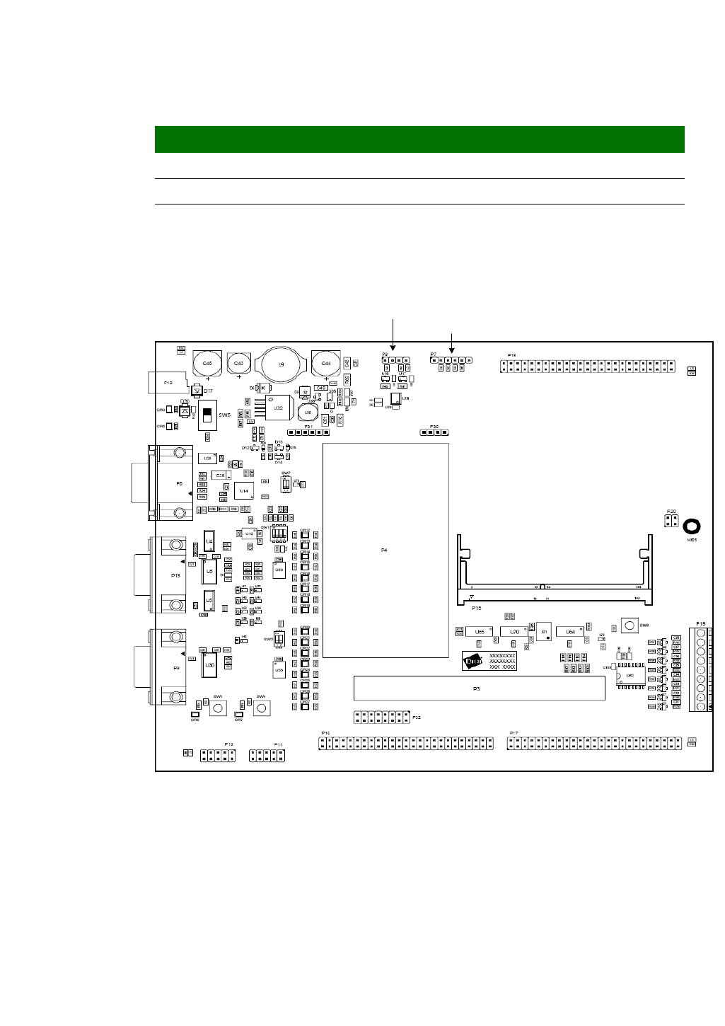
I2C and SPI header connectors
I2C header
connector, P8 The development board has a 4-pin I2C header connector, labeled P8.
Setting VGA interface GPIO15 GPIO40 / GPIO41
ON Disabled DCD_A# TXD_C/RXD_C
OFF Enabled (default) EXT_VGA_OSC VGA_BLUE6/VGA_BLUE7
I2C header connector, P8
SPI header connector, P7
ABOUT THE DEVELOPMENT BOARD
I2C and SPI header connectors
34 ConnectCore 9c/Wi-9C Hardware Reference, Rev. B 01/2007
3
P8 pin assignment
SPI header
connector, P7 The development board has one 6-pin SPI header connector, labeled P7.
Important:
If you use the SPI header connector, Serial Port B must be disabled (in
software).
P7 pin assignment
All SPI signals are protected for the respective module’s boot strapping.
Pin Signal Description
1I2C_SDA I
2C serial data line
2+5V +5V
3I2C_SCL I
2C serial clock line
4 GND Ground
Pin Signal Description
1 +3.3V +3.3V
2 SPI_DOUT SPI data out
3 SPI_DIN SPI data in
4 SPI_CLK SPI clock
5 SPI_CS# SPI chip select
6 GND Ground
. . . . .
ABOUT THE DEVELOPMENT BOARD
Serial port connectors
www.digiembedded.com 35
. . . . . . . . . . . . . . . . . . . . . . . . . . . . . . . . . . . . . . . . . . . . . . . . . . . . . . . . . . . . . . . . . . . . . . . . . . . . . . . . . .
Serial port connectors
The development board has four serial ports: A (P13), B (P9), C (P10), and D (P11).
Serial ports A and B support full EIA-232 functionality; serial ports C and D do not.
Serial port A
(EIA-232/422/485)
connector, P13
The serial port A connector is a single DB-9 male connector for EIA-232/EIA-485
switchable mode, labeled P13. The serial port A interface corresponds to NS9360
serial port A, and is a switch-selectable EIA-232/422/485 interface with a maximum
baud rate of 921 kbps (see “Serial Port A switch, SW1” on page 31). Each signal is
available with its status LED, and all status LEDs are bi-color, red or green.
Serial port A
diagram This diagram shows the switch-selectable EIA-232/422/485 interface:
Serial port D, P11
Serial port
B, P9
Serial port
A, P13
Serial port C, P10
ABOUT THE DEVELOPMENT BOARD
Serial port connectors
36 ConnectCore 9c/Wi-9C Hardware Reference, Rev. B 01/2007
3
P13 connector pin
assignment
Serial port B
(EIA-232)
connector, P9
The serial port B connector is a single, DB-9 male connector, labeled P9. The serial
port B interface corresponds to NS9360 serial port B, and is a standard EIA-232
interface with a maximum baud rate of 921 kbps. Each signal is available with its
LED, and all status LEDs are bi-color, red or green.
The serial port B line driver can be disabled using Switch 2 (see “Serial Port B
switch, SW2” on page 32).
EIA-422/485
transceiver
Control
Switch
logic
NS9360 serial port A signals
EIA-232
transceiver
EIA-232#/485
DB-9
connector
Switch 1
1
2
3
4
On Off
Auto power down
4W#/2W
TERM
Pin EIA-232
signal EIA-232 signal
description EIA-422/485
4/8 wire EIA-485 2-wire
1DCD#
1Data Carrier Detect CTS- (B)
2 RXD Receive Data RXD+ (A) DATA+ (A)
3 TXD Transmit Data TXD+ (A)
4 DTR# Data Terminal Ready RTS- (B)
5 GND Ground GND GND
6 DSR# Data Set Ready RXD- (B) DATA- (B)
7 RTS# Request to Send RTS+ (A)
8 CTS# Clear to Send CTS+ (A)
9 RI# Ring Indicator TXD- (B)
1. When the VGA (enable) switch, SW7, is OFF (default), DCD is not available.
Shell is chassis GND.

. . . . .
ABOUT THE DEVELOPMENT BOARD
Serial port connectors
www.digiembedded.com 37
P9 connector pin
assignment
Serial port C
header connector,
P10
The serial port C header connector is a 2x5-pin serial port, labeled P10. The
connector is a UART interface, with signals available on TTL-level. The serial port C
interface corresponds to NS9360 serial port C.
The serial port C interface signals are available on TTL-level, and support only the
TXD, RXD, RTS#, and CTS# signals, where # indicates an active low signal. These
pins default to LCD or DIGITAL_I/O signals when switch 7 is configured for VGA
functionality (see “VGA (enable) switch, SW7” on page 32).
P10 connector pin
assignment
Serial port D
header connector,
P11
The serial port D header connector is a 2x5-pin serial port, labeled P11. The
connector is a UART interface, with signals available on TTL-level. The serial port D
interface corresponds to NS9360 serial port D.
Pin Signal Description
1 DCD# Data Carrier Detect
2 RXD Receive Data
3 TXD Transmit Data
4 DTR# Data Transmit Ready
5 GND Ground
6 DSR# Data Set Ready
7 RTS# Request to Send
8 CTS# Clear to Send
9 RI# Ring Indicator
Pin Signal Description VGA enabled (SW7)
1 Not connected n/a n/a
2 Not connected n/a n/a
3 RXD_C Receive Data LCD_D17
4 RTS_C# Request to Send DIGITAL_IO_9
5 TXD_C Transmit Data LCD_D16
6 CTS_C# Clear to Send DIGITAL_IO_10
7 Not connected n/a n/a
8 Not connected n/a n/a
9 GND Ground n/a
10 +3.3V Power n/a

ABOUT THE DEVELOPMENT BOARD
Serial port connectors
38 ConnectCore 9c/Wi-9C Hardware Reference, Rev. B 01/2007
3
The serial port D interface signals are available on TTL-level and support only the
TXD, RXD, RTS#, and CTS# signals, where # indicates an active low signal. These
pins default to GPIO signals 44-47. To use the pins for serial port D functions, you
need to configure them in software.
P11 connector pin
assignment Pin Signal Description Defaults to
1 Not connected n/a n/a
2 Not connected n/a n/a
3 RXD_D Receive Data GPIO45
4 RTS_D# Request to Send GPIO46
5 TXD_D Transmit Data GPIO44
6 CTS_D# Clear to Send GPIO47
7 Not connected n/a n/a
8 Not connected n/a n/a
9 GND Ground n/a
10 +3.3V Power n/a
. . . . .
ABOUT THE DEVELOPMENT BOARD
VGA connector / External LCD clock
www.digiembedded.com 39
. . . . . . . . . . . . . . . . . . . . . . . . . . . . . . . . . . . . . . . . . . . . . . . . . . . . . . . . . . . . . . . . . . . . . . . . . . . . . . . . . .
VGA connector / External LCD clock
VGA connector,
P6 The VGA connector is a 15-pin female connector, labeled P6.
P6 pin assignment
External
LCD clock,
G1
VGA
connector,
P6
Pin Signal Comment
1 VGA_RED
2 VGA_GREEN
3 VGA_BLUE
4 NC (Monitor ID2) Monitor ID2 is not implemented on the
development board
5GND
6 VGA_GND (RED_RETURN)
7 VGA_GND (GREEN_RETURN)
8 VGA_GND (BLUE_RETURN)
9NC

ABOUT THE DEVELOPMENT BOARD
Development board SO-DIMM connector, P15
40 ConnectCore 9c/Wi-9C Hardware Reference, Rev. B 01/2007
3
External LCD
clock, G1 An external LCD controller clock is provided to avoid picture quality deterioration
due to the low-emission spread spectrum clock used on the module.
G1 is a 48MHz oscillator that supports resolutions up to 640 x 480. The maximum
NS9360 external LCD clock frequency is 90MHz. The frequency is divided by 2 before
being used as the LCD clock source. For more information, see "Sample
applications," beginning on page 61.
. . . . . . . . . . . . . . . . . . . . . . . . . . . . . . . . . . . . . . . . . . . . . . . . . . . . . . . . . . . . . . . . . . . . . . . . . . . . . . . . . .
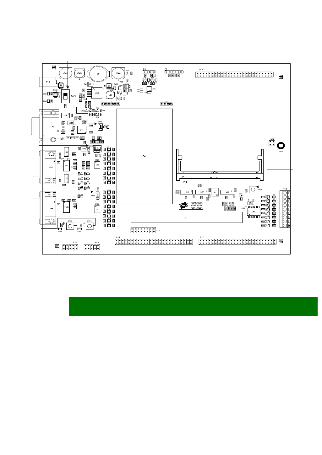
Development board SO-DIMM connector, P15
Manufacturer part number: AMP INCORPORATED 390112-1
P15 is a 144-pin SO-DIMM connector on the development board. Plug the
ConnectCore 9C/Wi-9C module SO-DIMM connector, P3, into P15.
Note:
The clearance between the module and your development board must be
2.54mm (0.10”).
10 GND (SYNC_RETURN)
11 NC (Monitor ID0) Monitor ID0 is not implemented on the
development board
12 NC
13 HSYNC
14 VSYNC
15 NC
Pin Signal Comment
. . . . .
ABOUT THE DEVELOPMENT BOARD
Development board SO-DIMM connector, P15
www.digiembedded.com 41
Bird’s-eye view
Close-up
Inserting the
module into the
SO-DIMM
connector
To be sure you insert the module into the SO-DIMM connector properly, review these
steps and figures:
1Align the module key with the housing key (see Figure 1).
2Slide the module into the housing (see Figure 1),
3Push the board down until the module snaps in (see Figure 2).
Be sure the metal latching edge engages the edge of the module.
SO-DIMM
connector,
P15
1
2
141
144
61 59
62 60
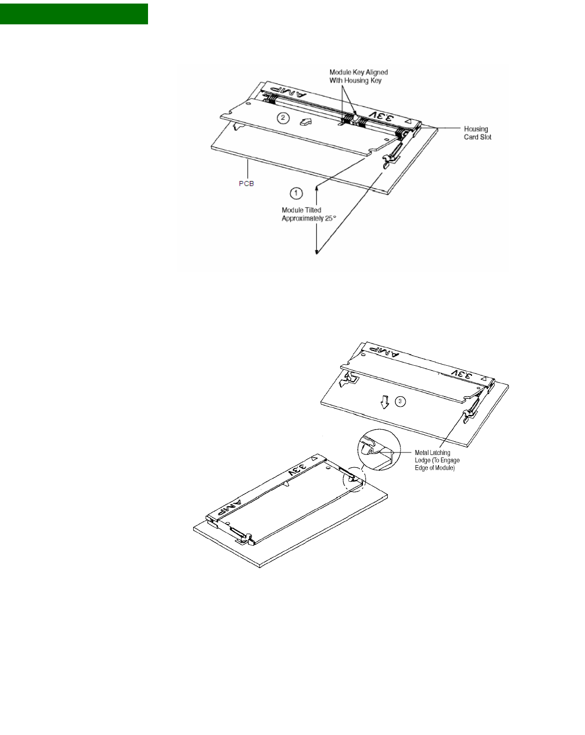
ABOUT THE DEVELOPMENT BOARD
Development board SO-DIMM connector, P15
42 ConnectCore 9c/Wi-9C Hardware Reference, Rev. B 01/2007
3
Figure 1: Inserting the module into the development board SO-DIMM connector, steps 1 &
2
Figure 2: Inserting the module into the development board SO-DIMM connector, step 3
P15 pin
assignment The pin assignment for P15 is the same as that for P3, the SO-DIMM connector on the
module. For the complete pin assignment list, see "Pin assignment by SO-DIMM pin
number," beginning on page 19.
. . . . .
ABOUT THE DEVELOPMENT BOARD
Application-specific expansion headers — P16 and P17
www.digiembedded.com 43
. . . . . . . . . . . . . . . . . . . . . . . . . . . . . . . . . . . . . . . . . . . . . . . . . . . . . . . . . . . . . . . . . . . . . . . . . . . . . . . . . .
Application-specific expansion headers — P16 and P17
Manufacturer part numbers:
SAMTEC TSM-125-02-L-DV
PINREX 212-92-25GB01
WAVE TECH EPS01-50-A-1-0-B
The development board provides two, 2x25-pin, 0.10” (2.54mm) pitch headers for
supporting application-specific daughter cards/expansion boards:
P16, Peripheral board header. Provides access to an 8-bit data bus, 8-bit
address bus, and control signals (for example, CS#, WE#), as well as I2C and
power. Using these signals, you can connect Digi-specific extension modules or
your own daughter card to the module’s address/data bus.
P17, Platform application header. Provides access to the serial port B signal,
one SPI interface, one USB channel, eight GPIOs, power, and the module’s IEEE
802.3af signals. You can attach Digi-provided application kits or your own
daughter card design.
Platform application board header, P17
Peripheral application board header, P16
ABOUT THE DEVELOPMENT BOARD
Application-specific expansion headers — P16 and P17
44 ConnectCore 9c/Wi-9C Hardware Reference, Rev. B 01/2007
3
Peripheral
application board
header, P16
Pin Signal Description /
Comment Pin Signal Description / Comment
1 GND Ground 2 DATA_0 Data bus
3 DATA_1 Data bus 4 DATA_2 Data bus
5 DATA_3 Data bus 6 GND Ground
7 DATA_4 Data bus 8 DATA_5 Data bus
9 DATA_6 Data bus 10 DATA_7 Data bus
11 GND Ground 12 Reserved (DATA_8) n/a
13 Reserved (DATA_9) n/a 14 Reserved (DATA10) n/a
15 Reserved (DATA_11) n/a 16 GND Ground
17 Reserved (DATA_12) n/a 18 Reserved (DATA_13) n/a
19 Reserved (DATA_14) n/a 20 Reserved (DATA_15) n/a
21 GND Ground 22 +3.3V 8 bit /16 bit#
3.3V selects 8-bit data bus
23 GND Ground 24 +3.3V Power
25 +3.3V Power 26 ADDRESS_0 Address bus
27 ADDRESS_1 Address bus 28 ADDRESS_2 Address bus
29 ADDRESS_3 Address bus 30 GND Ground
31 ADDRESS_4 Address bus 32 ADDRESS_5 Address bus
33 ADDRESS_6 Address bus 34 ADDRESS_7 Address bus
35 GND Ground 36 Reserved (ADDRESS_8) n/a
37 Reserved (ADDRESS_9) n/a 38 GND Ground
39 CS# Static memory chip select 0 40 I2C_SDA / GPIO71 I2C serial data line
41 WE# Write enable 42 OE# Output enable
43 I2C_SCL / GPIO70 I2C serial clock line 44 PERI_INT# USER_PUSH_BUTTON2 /
PERI_INT0# / GPIO69
45 +3.3V Power 46 +3.3V Power
47 PERI_GPIO0 DIGITAL_IO_9 /
UART3_RTS /
GPIO42_PRT
48 PERI_GPIO1 DIGITAL_IO_10 /
UART3_CTS# / GPIO43_PRT
49 RESET_OUT Connected to inverted
BUFFENR# signal
50 GND Ground

. . . . .
ABOUT THE DEVELOPMENT BOARD
Application-specific expansion headers — P16 and P17
www.digiembedded.com 45
Platform
application board
header, P17
Pin Signal GPIO/Other Pin Signal GPIO/Other
1 GND n/a 2 TXD_B / SPI_DO GPIO0
3 RXD_B / SPI_DI GPIO1 4 CTS_B# GPIO3
5 DSR_B# GPIO5 6 DCD_B# / SPI_CE GPIO7
7 RI_B# / SPI_CLK GPIO6 8 DTR_B# GPIO4
9 RTS_B# GPIO2 10 GND n/a
11 I2C_SCL GPIO70 12 I2C_SDA GPIO71
13 GND n/a 14 RST# System reset
15 GND n/a 16 DP1 n/a
17 DM1 n/a 18 GND n/a
19 LCD_D2 GPIO26 19 LCD_D3 GPIO27
21 TXD_D GPIO44 22 RXD_D GPIO45
23 GND n/a 24 +3.3V n/a
25 GND n/a 26 +3.3V n/a
27 DIGITAL_IO_1 GPIO23 28 DIGITAL_IO_2 GPIO16
29 DIGITAL_IO_3 GPIO17 30 DIGITAL_IO_4 GPIO18
31 USER_LED_1 /
DIGITAL_IO_5
GPIO66 32 GND n/a
33 USER_LED_2 /
DIGITAL_IO_6
GPIO67 34 DIGITAL_IO_9 / RTS_C# GPIO42
35 DIGITAL_IO_10 / CTS_C# GPIO43 36 GND n/a
37 Not connected n/a 38 Not connected n/a
39 Not connected n/a 40 Not connected n/a
41 Not connected n/a 42 Not connected n/a
43 Not connected n/a 44 Not connected n/a
45 Not connected n/a 46 Not connected n/a
47 Not connected n/a 48 Not connected n/a
49 Not connected n/a 50 Not connected n/a
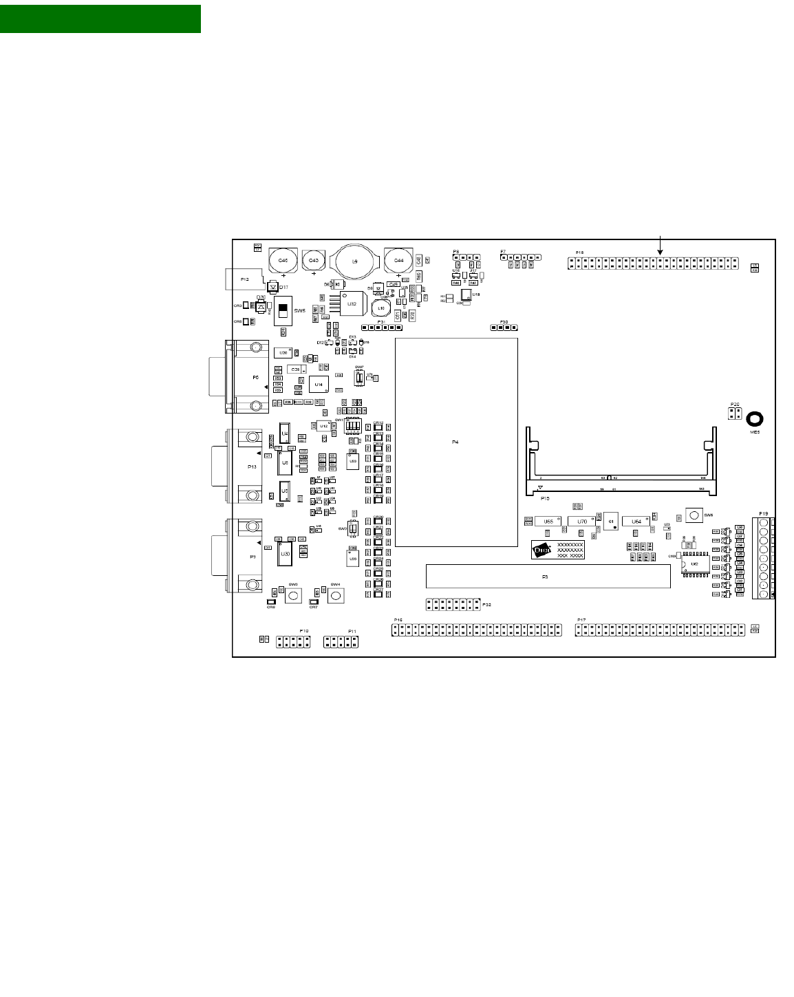
ABOUT THE DEVELOPMENT BOARD
LCD application board header, P18
46 ConnectCore 9c/Wi-9C Hardware Reference, Rev. B 01/2007
3
. . . . . . . . . . . . . . . . . . . . . . . . . . . . . . . . . . . . . . . . . . . . . . . . . . . . . . . . . . . . . . . . . . . . . . . . . . . . . . . . . .
LCD application board header, P18
Manufacturer part numbers:
SAMTEC TSM-125-02-L-DV
PINREX 212-92-25GB01
WAVE TECH EPS01-50-A-1-0-B
The LCD application header, P18, is a 2x25-pin, 0.10” (2.54mm) pitch header that
provide access to the LCD signals and SPI signals for touch controller purposes. Use
with the Digi-provided LCD application kit or attach your own LCD application
board.
LCD application header, P18

. . . . .
ABOUT THE DEVELOPMENT BOARD
LCD application board header, P18
www.digiembedded.com 47
P18 pin
assignment
Pin Signal GPIO/Other Pin Signal GPIO/Other
1 GND N/A 2 LCD_D0 GPIO24
3 LCD_D1 GPIO25 4 LCD_D2 GPIO26
5 LCD_D3 GPIO27 6 GND N/A
7 LCD_D4 GPIO28 8 LCD_D5 GPIO29
9 LCD_D6 GPIO30 10 LCD_D7 GPIO31
11 GND N/A 12 LCD_D8 GPIO32
13 LCD_D9 GPIO33 14 LCD_D10 GPIO34
15 LCD_D11 GPIO35 16 GND N/A
17 LCD_D12 GPIO36 18 LCD_D13 GPIO37
19 LCD_D14 GPIO38 20 LCD_D15 GPIO39
21 GND N/A 22 LCD_D16 / TXD_C# GPIO40
23 LCD_D17 / RXD_C# GPIO41 24 GND (Reserved) LCD_D18
25 GND (Reserved) LCD_D19 26 GND N/A
27 GND (Reserved) LCD_D20 28 GND (Reserved) LCD_D21
29 I2C_SDA GPIO71 30 I2C_SCL GPIO70
31 GND N/A 32 LCD_CLOCK GPIO20
33 LCD_BIAS GPIO22 34 LCD_HSYNC GPIO19
35 LCD_VSYNC GPIO21 36 PENIRQ# GPIO18
37 LCD_PWREN# GPIO23 38 +3.3V N/A
39 GND (Reserved) TSPX 40 GND (Reserved) TSPY
41 GND (Reserved) TSMX 42 GND (Reserved) TSMY
43 +3.3V N/A 44 RI_B# / SPI_CLK GPIO6
45 DCD_B# / SPI_CE# GPIO7 46 TXD_B / SPI_DO GPIO0
47 RXD_B / SPI_DI GPIO1 48 +3.3V N/A
49 GND TOUCH/SPI# 50 GND N/A
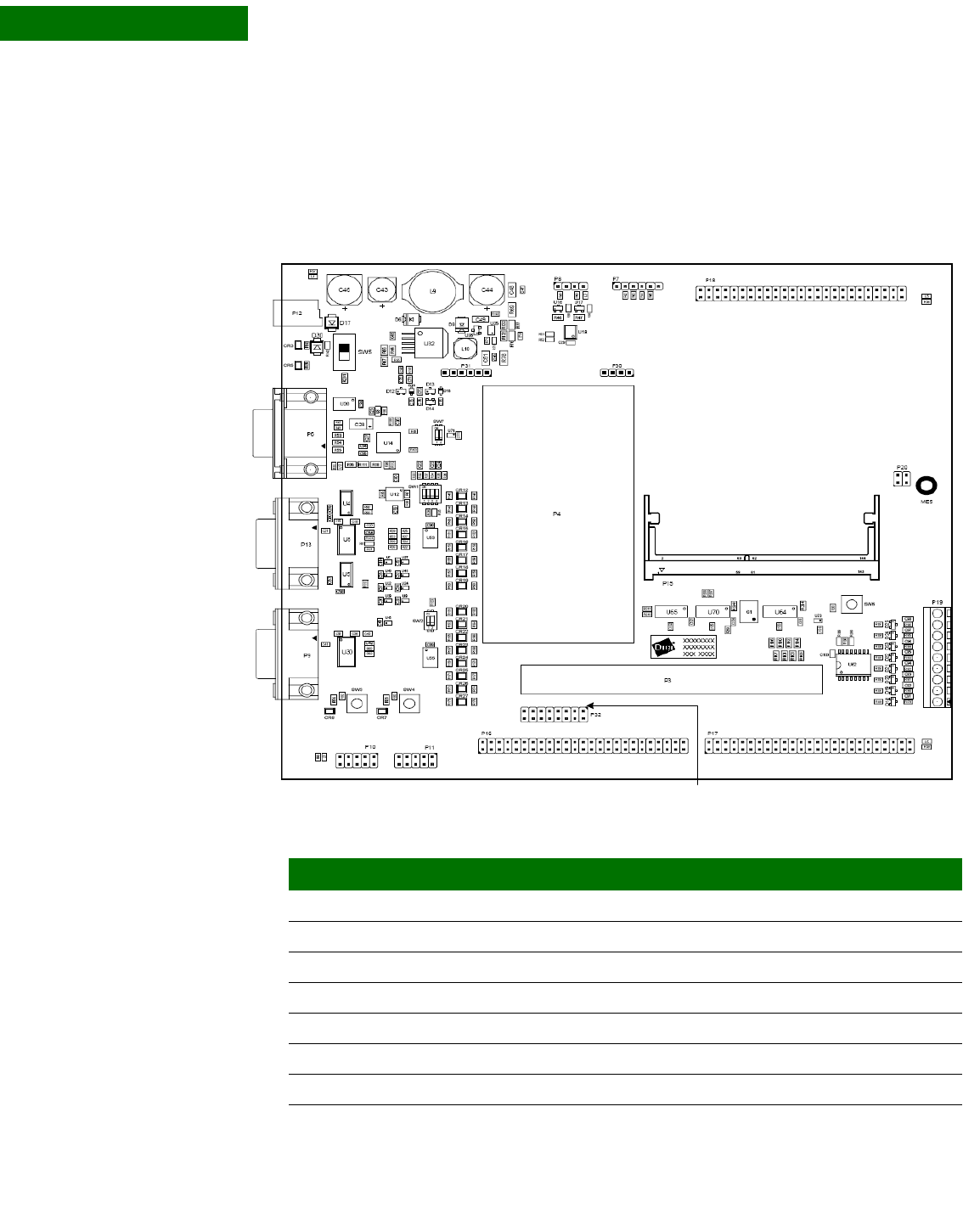
ABOUT THE DEVELOPMENT BOARD
USB Device application header, P32
48 ConnectCore 9c/Wi-9C Hardware Reference, Rev. B 01/2007
3
. . . . . . . . . . . . . . . . . . . . . . . . . . . . . . . . . . . . . . . . . . . . . . . . . . . . . . . . . . . . . . . . . . . . . . . . . . . . . . . . . .
USB Device application header, P32
Manufacturer part number: EPT 972-08009-21
The USB Device application header, P32, is a press fit 2x8 pin, straight RM2.54
(Y=6.7mm) header. Use this header to connect an external USB Device application
to the development board, which then provides USB Device functionality.
P32 pin
assignment
USB Device application header, P32
Pin Signal Comment
1 +3.3V
2 GND
3+5V
4 GND
5 DIGITAL_IO_9 / UART3_RTS# / GPIO42_PRT USB_VP functionality
6 DIGITAL_IO_10 / UART3_CTS# / GPIO43_PRT USB_VM functionality
7 GND
8 GND
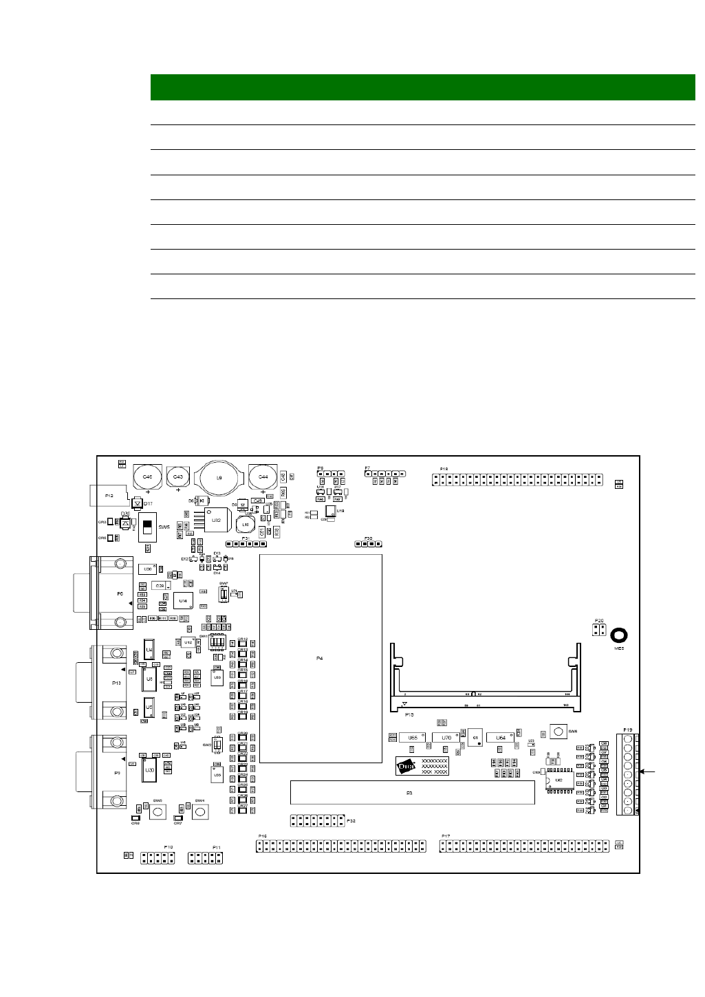
. . . . .
ABOUT THE DEVELOPMENT BOARD
Digital I/O, P19
www.digiembedded.com 49
. . . . . . . . . . . . . . . . . . . . . . . . . . . . . . . . . . . . . . . . . . . . . . . . . . . . . . . . . . . . . . . . . . . . . . . . . . . . . . . . . .
Digital I/O, P19
Manufacturer part number: BlockMaster MTS0900T
The Digital I/O connector, P19, is a MTS, 9-pin terminal block for PCB RM3.81.
9 GPIO44 / UART4_TXD / SPID_DO_PRT USB_OE# functionality
10 USER_LED_3 / DIGITAL_IO_7 / GPIO48 USB_SPND functionality
11 USER_LED_4 / DIGITAL_IO_8 / GPIO49 USB_SPEED functionality
12 GPIO45 / UART4_RXD / SPID_DI_PRT USB_RCV functionality
13 GPIO46 / UART4_RTS#_PRT USB_ENUM functionality
14 GND
15 I2C_SDA / GPIO71_PRT
16 I2C_SCL / GPIO70_PRT
Pin Signal Comment
Digital I/O,
P19
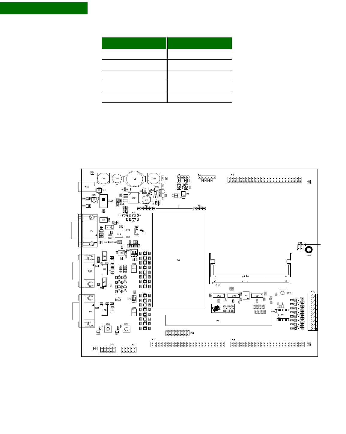
ABOUT THE DEVELOPMENT BOARD
Power over Ethernet (PoE) connectors
50 ConnectCore 9c/Wi-9C Hardware Reference, Rev. B 01/2007
3
P19 pin
assignment
. . . . . . . . . . . . . . . . . . . . . . . . . . . . . . . . . . . . . . . . . . . . . . . . . . . . . . . . . . . . . . . . . . . . . . . . . . . . . . . . . .
Power over Ethernet (PoE) connectors
The development board provides three PoE connectors: P20, P30, and P31.
The PoE connector, P20, captures PoE signals from the module on the development
board and routes them to the PoE module connector, P30. See “802.3af Power over
Ethernet (PoE) pass-through connector, P5” on page 13 for more information.
The P30 and P31 connectors support the IEEE 802.3af PoE application module.
Pin Signal Pin Signal
1 I2C_IO_0 2 I2C_IO_1
3 I2C_IO_2 4 I2C_IO_3
5 I2C_IO_4 6 I2C_IO_5
7 I2C_IO_6 8 I2C_IO_7
9 GND
PoE
connector,
P20
PoE sockets, P30 & P31

. . . . .
ABOUT THE DEVELOPMENT BOARD
Power over Ethernet (PoE) connectors
www.digiembedded.com 51
P30 is the input connector of the PoE module, providing access to the PoE
signals coming from the ConnectCore 9C/Wi-9C module through P20.
P31 provides the output voltage and ground signals from the PoE module. When
you use PoE, this output voltage powers the development board; you do not
need the main power supply.
802.3afPoE
connector, P20 Manufacturer part numbers:
AMP INCORPORATED 5-146256-2
AMP INCORPORATED 5-146257-2
SAMTEC TSW-102-07-L-D
P20 pins are allocated as shown:
P30 connector Manufacturer part number: Samtec SLW-104-01-G-S
The P30 input connector is a 1x4 pin socket with these characteristics: SLW, THT,
RM2.54 (h=4.57mm).P30 pins are allocated as shown:
P31 connector Manufacturer part number: Samtec SLW-106-01-G-S
The P31 connector is a 1x6 pin socket with these characteristics: SLW, THT, RM2.54
(h=4.57mm). P31 pins are allocated as shown:
Pin Signal Actual signal name Description
1 POE_TX_CT POE_RJ45_4/5 Ethernet connector pins 4 and 5
2 POE_RJ45_7/8 POE_RX_CT Ethernet transformer receive CT
3 POE_RX_CT POE_RJ45_7/8 Ethernet connector pins 7 and 8
4 POE_RJ45_4/5 POE_TX_CT Ethernet transformer transmit CT
Pin Signal
1 POE_TX_CT
2POE_RX_CT
3 POE_RJ45_4/5
4 POE_RJ45_7/8
Pin Signal Pin Signal
1 +12V_POE 2 +12V_POE
3GND 4GND
5 POE_GND 6 POE_GND
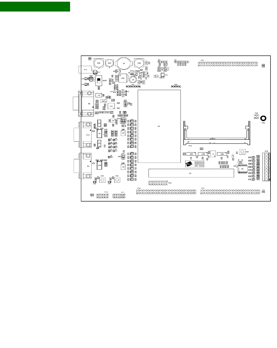
ABOUT THE DEVELOPMENT BOARD
Through-hole prototyping (wrap-field) area, P3 and P4
52 ConnectCore 9c/Wi-9C Hardware Reference, Rev. B 01/2007
3
. . . . . . . . . . . . . . . . . . . . . . . . . . . . . . . . . . . . . . . . . . . . . . . . . . . . . . . . . . . . . . . . . . . . . . . . . . . . . . . . . .
Through-hole prototyping (wrap-field) area, P3 and P4
The through-hole prototyping area has two parts, P3 and P4.
Through-hole
signal rail, P3 Manufacturer part number: SAMTEC TSW-136-xx-D
where xx is the length of the header pins; you choose the connector that best fits
your application. P3 is a four-column, 144-signal, through-hole signal rail that
provides 1:1 access to all module signals. You can solder every 2.54mm through-hole
header. The size of the P3 connector is 4x36 pins (see the drawing following the
next paragraph) — note, however, that you can solder only a smaller header onto
the connector. If you want to solder a complete header over the through-hole signal
rail, use 2 headers of 2x36 pins each.
The signal assignments for P3 are the same as those for the edge connector, P3, on
the module; see "Pin assignment by SO-DIMM pin number," beginning on page 19, for
detail.
Through-hole signal rail, P3
Through-hole
prototyping
(wrap-field)
area, P4
. . . . .
ABOUT THE DEVELOPMENT BOARD
Through-hole prototyping (wrap-field) area, P3 and P4
www.digiembedded.com 53
Wrap-field area,
P4 P4 is a wrap field area that allows you to connect through-hole components. The
+3.3, +5V, and GND buses run along the top edge of the wrap-field area.
Pin 1
Pin 4
Pin 141
Pin 144
+3.3V
+5V
GND
.
.
.
.
.
.
.
.
.
.
.
.
.
.
.
.
.
.
.
.
.
.
.
.
.
.
.
.
.
.
.
.
.
.
.
.
.
.
.
.
.
.
.
.
.
.
.
.
.
.
.
.
.
.
.
.
.
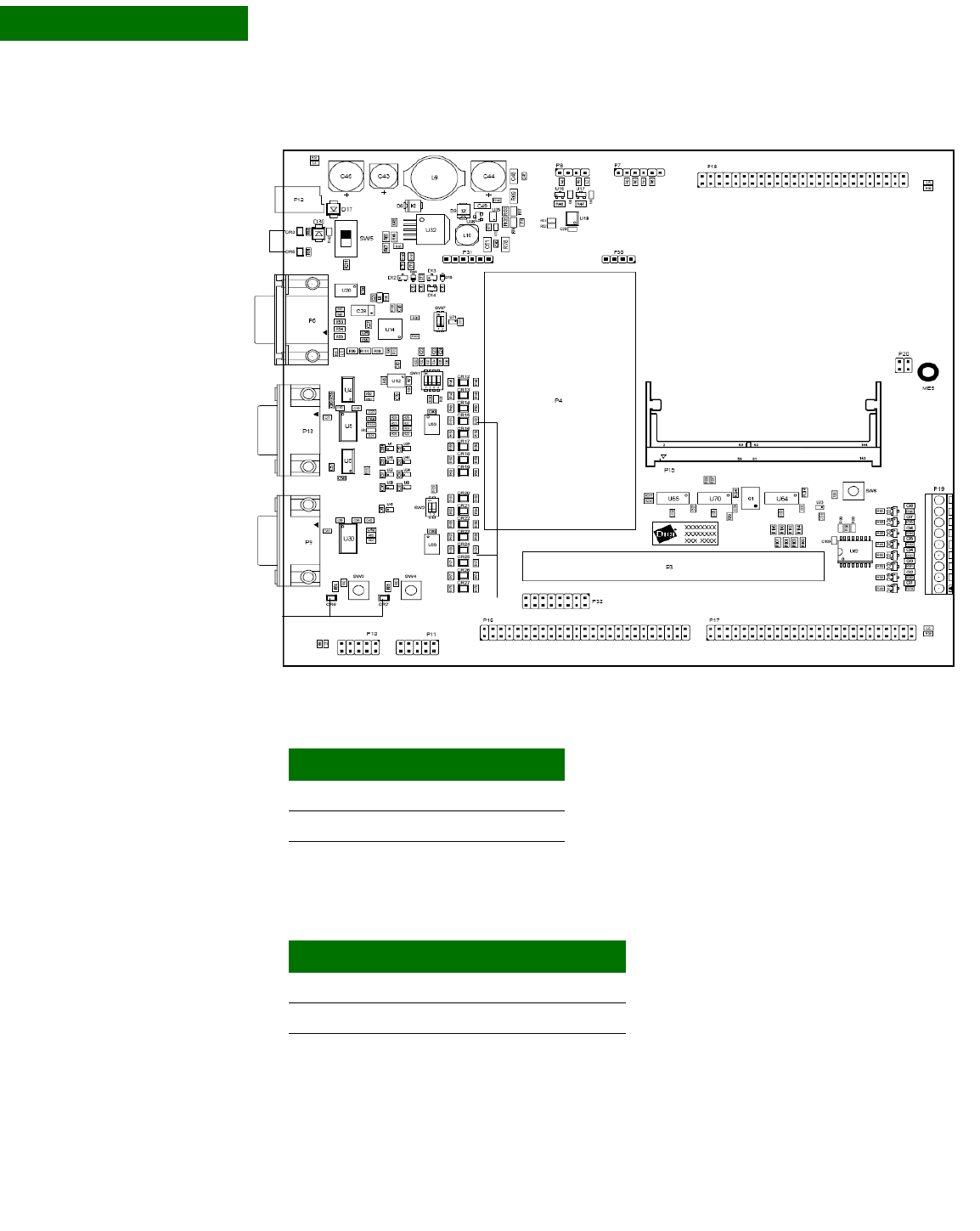
ABOUT THE DEVELOPMENT BOARD
Development board LEDs
54 ConnectCore 9c/Wi-9C Hardware Reference, Rev. B 01/2007
3
. . . . . . . . . . . . . . . . . . . . . . . . . . . . . . . . . . . . . . . . . . . . . . . . . . . . . . . . . . . . . . . . . . . . . . . . . . . . . . . . . .
Development board LEDs
Power LEDs, CR3
and CR5 The power LEDs are single-color (RED) LEDs, located below the power jack, P12.
User LEDs, CR6
and CR7 The user LEDs are single-color (GREEN) LEDs, located next to switches 3 and 4 on
the development board.
Serial LEDs The serial port A LEDs are to the right of the serial port A (EIA-232/EIA-485)
connector, on the left side of the wrap-field area. The serial port B LEDs are to the
right of the serial port B(EIA-232) connector, on the left side of the wrap-field area.
User LEDs,
CR6 & CR7
Power
LEDs
Serial status LEDs
A
B
LED Condition when ON
CR3 5V power is present
CR5 3.3V power is present
LED Condition when ON
CR6 Value of GPIO48 is a logic 0
CR7 Value of GPIO49 is a logic 0.
. . . . .
ABOUT THE DEVELOPMENT BOARD
Current Measurement Option (CMO)
www.digiembedded.com 55
The LED indicators are dual-state, and are connected to the TTL side of the EIA
transceivers.
Green represents a negative voltage on the DB9 connector pin.
Red represents a positive voltage DB9 connector pin.
The intensity and color of the LED will change when the voltage is switching.
. . . . . . . . . . . . . . . . . . . . . . . . . . . . . . . . . . . . . . . . . . . . . . . . . . . . . . . . . . . . . . . . . . . . . . . . . . . . . . . . . .
Current Measurement Option (CMO)
The Current Measurement Option uses 0.025R series resistors to measure the
current on the development board’s +3.3V (R78) and +5V (R69) power supplies.
Serial port A LEDs Name Function Serial Port B LEDs Name Function
CR12 DCD# CR20 DCD#
CR13 RI# CR21 RI#
CR14 DSR# CR22 DSR#
CR15 DTR# CR23 DTR#
CR16 CTS# CR24 CTS#
CR17 RTS# CR25 RTS#
CR18 RXD CR26 RXD
CR19 TXD CR27 TXD
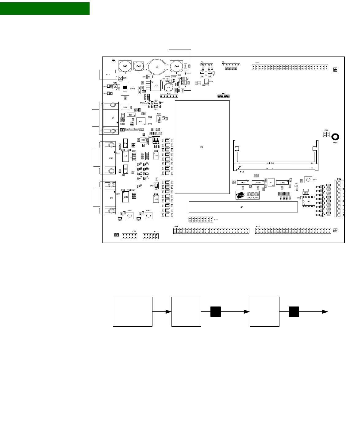
ABOUT THE DEVELOPMENT BOARD
Current Measurement Option (CMO)
56 ConnectCore 9c/Wi-9C Hardware Reference, Rev. B 01/2007
3
How the CMO
works This drawing shows how the Current Measurement Option works.
To measure the load current used on different power supplies, measure DC voltage
across the sense (CMO) resistor. The value of the resistor is 0.025R ± 1%. Calculate
the current using this equation: I = E/R
where
I = current in Amps
E = measured voltage in Volts
R = 0.025 Ohms
Current
measurement
option, CMO
R69
R78
Power
connector
+9VDC -
+30VDC
Current
Measurement
Option
Current
Measurement
Option
R69
0.025R
R78
0.025R
+5VDC
+3,3VDC
+5V
power
controller
+3.3V
power
controller
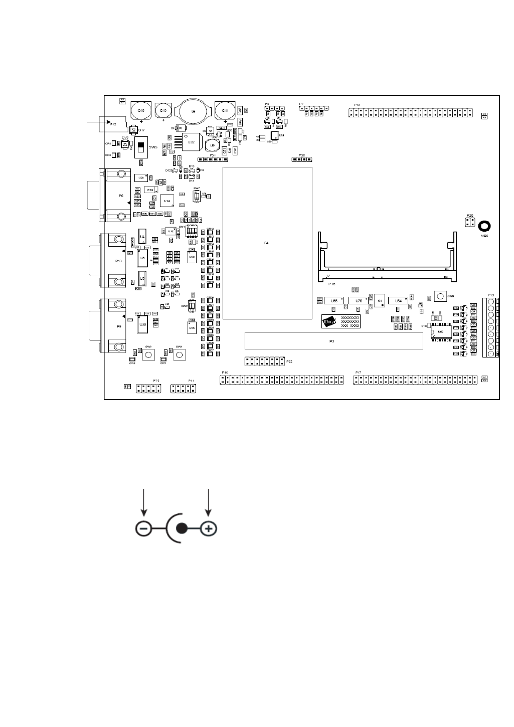
. . . . .
ABOUT THE DEVELOPMENT BOARD
Power jack, P12
www.digiembedded.com 57
. . . . . . . . . . . . . . . . . . . . . . . . . . . . . . . . . . . . . . . . . . . . . . . . . . . . . . . . . . . . . . . . . . . . . . . . . . . . . . . . . .
Power jack, P12
The power jack is a barrel connector with 9-30VDC operating range. The power jack
is labeled P12 on the development board. This figure schematically represents the
power jack’s polarity:
. . . . . . . . . . . . . . . . . . . . . . . . . . . . . . . . . . . . . . . . . . . . . . . . . . . . . . . . . . . . . . . . . . . . . . . . . . . . . . . . . .
Test points
The development board provides five test points that can be identified by board
label or test point number. The board labels are adjacent to each test point on the
board. The test point numbers are in the development board schematic drawings.
Power
jack, P12
Ground 9-30 VDC

ABOUT THE DEVELOPMENT BOARD
Factory default interface configuration for development board
58 ConnectCore 9c/Wi-9C Hardware Reference, Rev. B 01/2007
3
Numbers and
description
Factory default interface configuration for development
. . . . . . . . . . . . . . . . . . . . . . . . . . . . . . . . . . . . . . . . . . . . . . . . . . . . . . . . . . . . . . . . . . . . . . . . . . . . . . . . . .
board
These interfaces are enabled as shown per the factory default configuration:
Test point Label Source/Comment
TP36 +12V +Charge pump off of DC/DC regulator (U32)
TP37 -12V - Charge pump off of DC/DC regulator (U32)
TP38 +5V DC/DC regulator (U32) with 9-30VDC input
TP41 +3.3V DC/DC regulator (U35) with +5V input
TP42 GND Common Ground return
Interface Factory default status
LCD VGA Enabled
I2C (5V tolerant) Enabled
I2C user-driven I/Os Enabled
EIA-232 Serial Port A Enabled (No DCD unless LCD_VGA is disabled)
EIA-485 Serial Port A Disabled
EIA-232 Serial Port B Enabled (Full modem support)
TTL Serial Port C Disabled (Disabled when LCD_VGA is enabled)
TTL Serial Port D Disabled (GPIO signals 44-47 default as GPIOs)
SPI Serial Port B Disabled (No SPI unless EIA-232 Serial Port B is disabled)

59
LCD and USB Configuration
CHAPTER 4
This chapter addresses module specifics pertaining to the LCD and USB
interfaces.
See the application note “LCD Displays Supported by the NetSilicon NS9750/NS9360
Processors” (available on http://www.digiembedded.com) for additional
information about the application-specific configuration and capabilities of the LCD
controller on the ConnectCore 9C/Wi-9C module.
. . . . . . . . . . . . . . . . . . . . . . . . . . . . . . . . . . . . . . . . . . . . . . . . . . . . . . . . . . . . . . . . . . . . . . . . . . . . . . . . . .
LCD displays
There are seven categories of LCD displays, all of which the module supports:
Color TFT (thin film transistor, also called active matrix (AM)):
–18-bit
Six types of STN (super twisted nematic, also called passive matrix (PM)):
–Three single panel displays
–Three dual panel displays
Each STN display is either color or monochrome:
–Color display: Up to 8-pin using color-enhancing palette RAM
–Monochrome display: Up to 8-pin or 4-pin using grayscale-enhancing palette
RAM
Control and data
pins The ConnectCore 9C/Wi-9C LCD interface has six control pins. The number of data
pins depends on the display type. Displays typically require 4–6 control pins. The
next two tables list the control pins and the data pins, respectively.

LCD AND USB CONFIGURATION
LCD displays
60 ConnectCore 9c/Wi-9C Hardware Reference, Rev. B 01/2007
4
LCD controller
control pins
LCD controller
data pins
Note:
Double-panel displays use twice as many pins but do not offer more color or
gray shades.
Colors and gray
shades The number of colors and gray shades correlates with the number of data pins but
also depends on color processing techniques and data-shifting techniques.
For exact values, see the NS9360 Hardware Reference, LCD Controller chapter,
“Number of Colors” and “Grayscaler.” You can access the NS9360 Hardware
Reference through the Jump Start Kit.
Pin # Signal name Type Description
89 CLPOWER Output LCD panel power enable
87 CLLP (HSYNC) Output Line synchronization pulse (STN)/horizontal synchronization pulse
(TFT)
46 CLCP Output LCD panel clock
44 CLFP Output Frame pulse (STN)/vertical synchronization pulse (TFT)
42 CLAC Output STN AC bias drive or TFT data enable output
38 CLLE Output Line end signal
Display type Number of data pins: Panel 1 Number of data pins: Panel 2
TFT—Color only
Color 18-bit 18 Not applicable
STN—Color
Single panel 8-bit 8 Not applicable
Dual panel 8-bit 8 8
STN—Monochrome
Single panel 4-bit 4 Not applicable
Dual panel 4-bit 4 4
Single panel 8-bit 8 Not applicable
Dual panel 8-bit 8 8

. . . . .
LCD AND USB CONFIGURATION
Sample applications
www.digiembedded.com 61
Sample displays ConnectCore 9C/Wi-9C uses an internal programmable palette-LUT and a grayscaler
to support different color-processing techniques; three sample displays are
provided here:
18-pin TFT display (for example, the SHARP LQ10D421). Accepts 18 color RGB
bits (6 bits per color) at a time. Only 16 bits are transferred from SDRAM: five
bits each for the three colors — R (red), G (green), and B (blue) — and a single
LSB (least significant bit) that is split into three equal values between R, G,
and B. This produces close to 216, or 64 thousand colors.
8-pin STN color display (for example, the SHARP LM057QC1T01). Shifts eight
color bits at a time: RGBRGBRG bits followed by BRGBRGBR bits followed by
GBRGBRGB, and so on. This produces color enhancing in 3375 color grades.
4-pin STN monochrome display (for example, the Grand Pacific
Optoelectronics GM0008-13). Shifts four monochrome bits at a time, resulting
in 15 gray shades (24 – 1).
Resolution The LCD resolution is programmable. These standard displays, with the following
resolutions, are supported:
QVGA = 320 x 240
VGA = 640 x 480
Lower resolution displays also are supported. Displays typically have programmable
vertical resolutions within a certain range, especially if they are used for TV
displays (to accommodate different television standards).
Refresh frequency The LCD refresh frequency is programmable. Lower refresh frequency drains less
power, but might flicker. TFT displays usually flicker less than STN displays, as they
have a transistor switch behind each pixel on the screen and can hold the capacitive
charge longer.
. . . . . . . . . . . . . . . . . . . . . . . . . . . . . . . . . . . . . . . . . . . . . . . . . . . . . . . . . . . . . . . . . . . . . . . . . . . . . . . . . .
Sample applications
The LCD interface uses memory as a video buffer. The display resolution is
determined by the product of three parameters: number of data bits x display
resolution x refresh frequency. This product cannot exceed the system bus
bandwidth allocated to the display.
Be aware that the actual bandwidth used by the display is:
display clock rate x number of bits per clock
For example, a clock rate of 50MHz with 16 bits of color yields a bandwidth of 100
MBps. To minimize bandwidth requirements, you might need to use an external
oscillator to get the exact rate.

LCD AND USB CONFIGURATION
Sample applications
62 ConnectCore 9c/Wi-9C Hardware Reference, Rev. B 01/2007
4
The ConnectCore 9C/Wi-9C development board has a 48MHz external oscillator and
resulting LCD clock of 24MHz. 16 bits of color requires 48 MBps for the display.
Default LCD
controller The default LCD controller configuration supported by the NS9360 is 640 x 480, with
8 bits for color. The bandwidth is guaranteed; the designer does not need to be
concerned with bandwidth use. Higher resolutions are possible but require care in
their setup and design.
Formula The ConnectCore 9C/Wi-9C module operates at 155 MHz system bus speed. This
speed grade results in 310 MBps bus bandwidth, as the bus is 4 bytes wide. For
bandwidth planning, this maximum bandwidth must be reduced to account for
overhead and read/write switching. The effective bandwidth is 1/2 of the system
bandwidth; that is, 155 MBps. This value is predicted as the worst case for the
ConnectCore 9C/Wi-9C. The architecture allocates half of the system bandwidth to
the module. The remaining four bus master peripherals (Ethernet TX, Ethernet RX,
peripheral bus bridge, and LCD controller) share the other half of the bandwidth.
The bandwidth assignment of these peripherals is programmable.
Use this formula to estimate the amount of bandwidth available for your LCD
display:
CPU bandwidth = 77.5 MBps
All other peripherals (including LCD) = 77.5 MBps
Example 1: 18-bit
VGA The 18-bit TFT display transfers 16 bits per pixel and generates the last two bits
inside the LCD controller. This display packs two-color RGB pixels into a single 4-
byte word.
The 18-bit VGA display (640 x 480), refreshing 60 times per second, requires 37
MBps:
2 x 640 x 480 x 60 = 37 MBps
40.5 MBps are left to all other peripherals. If the LCD refresh frequency increases to
70 Hz, the required bandwidth increases to 43 MBps.
Note:
The module LCD controller supports 18-bit VGA displays in most applications.
Supported TFT
displays Display type Refresh
frequency in Hz BW required for
display in MBps Display in MBps
BW left to other
peripherals in MBps
18b VGA (640 x 480) 50 31 46.5
60 37 40.5
70 43 34.5

. . . . .
LCD AND USB CONFIGURATION
USB configuration
www.digiembedded.com 63
. . . . . . . . . . . . . . . . . . . . . . . . . . . . . . . . . . . . . . . . . . . . . . . . . . . . . . . . . . . . . . . . . . . . . . . . . . . . . . . . . .
USB configuration
When you purchase the Ethernet plus USB hub version of the ConnectCore 9C/Wi-9C
module, the USB hub is installed on the module.
On modules without USB, NS9360 dedicated USB signals are brought out to the
Application header, P17:
See also “Power requirements” on page 67 for power required per USB port.
“USB interface” on page 68 for information about integrating the module
without on-board USB and without need for USB.
“USB internal PHY DC electrical inputs and outputs” on page 77
P17 pin Signal Description
16 DP1 USB data (+)
17 DM1 USB data (-)
28 USB_OVRH# USB overcurrent
29 USB_PONH# USB power-on


65
Module Specifications
APPENDIX A
This appendix provides ConnectCore 9C/Wi-9C module specifications.
. . . . . . . . . . . . . . . . . . . . . . . . . . . . . . . . . . . . . . . . . . . . . . . . . . . . . . . . . . . . . . . . . . . . . . . . . . . . . . . . . .
Mechanical dimensions
ConnectCore 9C Length: 3.590 inches (91.19 mm)
Add (0.136 inches (3.45 mm) for USB and/or Ethernet connector overhang
Width: 2.055 inches (52.2 mm)
Height:
0.799 inches (20.3 mm) with Dual USB connector
0.712 inches (18.08 mm) with RJ-45 Ethernet connector
ConnectCore
Wi-9C
Length: 3.590 inches (91.19 mm)
–Add 0.136 inches (3.45 mm) for USB and/or Ethernet connector overhang
–Add 0.375 inches (8.95 mm) for RP-SMA antenna overhang
Width: 3.055 inches (77.60 mm)
Height:
–0.799 inches (20.3 mm) with dual USB connector
–0.712 inches (18.08 mm) with RJ-45 Ethernet connector

MODULE SPECIFICATIONS
Environmental information
66 ConnectCore 9C/Wi-9C Hardware Reference, Rev. B 01/2007
A
. . . . . . . . . . . . . . . . . . . . . . . . . . . . . . . . . . . . . . . . . . . . . . . . . . . . . . . . . . . . . . . . . . . . . . . . . . . . . . . . . .
Environmental information
ConnectCore 9C Operating temperature: -40° C to +85° C (-40° F to +185° F)
Storage temperature: -40° C to +125° C (-40° F to 257° F)
Relative humidity: 5% to 95% (non-condensing)
Altitude: 12,000 ft (3657.6 m)
ConnectCore
Wi-9C
Operating temperature: -30° C to +75° C (-22° F to +167° F)
Storage temperature: -40° C to +125° C (-40° F to 257° F)
Relative humidity: 5% to 95% (non-condensing)
Altitude: 12,000 ft (3657.6 m)
. . . . . . . . . . . . . . . . . . . . . . . . . . . . . . . . . . . . . . . . . . . . . . . . . . . . . . . . . . . . . . . . . . . . . . . . . . . . . . . . . .
Network interface
Ethernet Standard: IEEE 802.3
Physical layer: 10/100Base-T
Data rate: 10/100 Mbps (auto-sensing)
Mode: Full or half duplex (auto-sensing)
On-board connector: RJ-45 with magnetics (optional)
802.3af power pass-through (mid-span and end-span)
WLAN Standard: IEEE802.11b/g
–Frequency: 2.4 GHz
–Data rate: Up to 54 Mbps with fallback
–Modulation: DBPSK (1 Mbps), DQPSK (2 Mbps), CCK (11,5.5 Mbps), BPSK (6,9
Mbps), QPSK (12,18 Mbps), 16-QAM (24,36 Mbps), 64-QAM (48,54 Mbps)
–Transmit power: 16 dBm typical
–Receive sensitivity: -73 dBm @ 54 Mbps
Connector: 1/2 x RP-SMA or 2 x U.FL

. . . . .
MODULE SPECIFICATIONS
Power requirements
www.digiembedded.com 67
. . . . . . . . . . . . . . . . . . . . . . . . . . . . . . . . . . . . . . . . . . . . . . . . . . . . . . . . . . . . . . . . . . . . . . . . . . . . . . . . . .
Power requirements
ConnectCore 9C Module: 3.3VDC @ 0.75A max
USB interface: 5VDC @ 0.5A max per port (optional)
ConnectCore
Wi-9C
Module: 3.3V ± 5% @ 0.95A max, 0.70A typ
Optional USB: 5V ± 10% @ 1.0A max
Power up The rise time of both the 3.3V power supply and 5V power supply must be between
700 μs and 140 ms, and the inrush current must be limited to less than 2A.
. . . . . . . . . . . . . . . . . . . . . . . . . . . . . . . . . . . . . . . . . . . . . . . . . . . . . . . . . . . . . . . . . . . . . . . . . . . . . . . . . .
Real-time clock
The accuracy of the internal Real-Time Clock on the module’s processor is .15%.
. . . . . . . . . . . . . . . . . . . . . . . . . . . . . . . . . . . . . . . . . . . . . . . . . . . . . . . . . . . . . . . . . . . . . . . . . . . . . . . . . .
I2C signals
The I2C signals are multiplexed with GPIO.
Legend SO-DIMM pin #: Pin number assignment for signal
Signal: Pin name for each signal.
U/D: Indicates whether the pin has an internal pullup resistor or pulldown resistor.
•U — Pullup
•D— Pulldown
•Blank — Neither an internal pullup or pulldown resistor
OD (mA): The output drive of an output buffer.
I/O: Type of signal input (I), output (O), or input/output (I/O)
Signals SO-DIMM
Pin# Signal name GPIO U/D OD
(mA) I/O Description
55 iic_scl GPIO[34] U 4 I/O I2C serial clock line.
Duplicate on GPIO[70]
66 iic_sda GPIO[35] U 4 I/O I2C serial data line.
Duplicate on GPIO[71]

MODULE SPECIFICATIONS
USB interface
68 ConnectCore 9C/Wi-9C Hardware Reference, Rev. B 01/2007
A
. . . . . . . . . . . . . . . . . . . . . . . . . . . . . . . . . . . . . . . . . . . . . . . . . . . . . . . . . . . . . . . . . . . . . . . . . . . . . . . . . .
USB interface
USB Host The USB Host consists of a USB Host controller that conforms to the Open Host
Controller Interface (OHCI) specification and a wrapper to interface the module to
the rest of the system. The USB Host interfaces to the internal USB PHY provided by
the NS9360, and is connected to an optional hub on the module.)
USB Device The USB Device module provides a USB 2.0-compliant interface for both full-speed
(12Mbps) and low-speed (1.5 Mbps) operation. The module supports one
bidirectional endpoint and up to 10 unidirectional endpoints that can be individually
programmed for endpoint type (interrupt, bulk, or isochronous) and direction. Each
endpoint is assigned to a DMA channel in a multi-channel BBus DMA controller. The
USB Device module interfaces to either the internal NS9360 USB PHY or an external
USB PHY using GPIO.
Support Both USB Host and Device can be supported at the same time:
USB Device, in this case, must use the only the signals shown in the table in the
section "USB Device only," beginning on page 69.
USB Host can be on the module or external to the module. If USB Host is
external to the module, use only the signals shown in the table in the section
"No USB on module," beginning on page 68.
Note:
All output drivers for USB meet the standard USB driver specifications.
USB Host with
hub on module
Connect up to two ports using the dual USB connector, P6.
All hub signals out to the SO-DIMM edge connector, P3, are reserved for future
use.
No USB on
module
USB data lines are brought out on DM1 and DP1.
–Terminate DM1 and DP1 with 15K pulldowns, if not used.
OVR1# and PON1# are multiplexed with GPIO16 and GPIO17.
26 iic_scl GPIO[70] 8 I/O I2C serial clock line.
Primary on GPIO[34]
24 iic_sda GPIIO[71] 8 I/O I2C serial data line.
Primary on GPIO[35]
SO-DIMM
Pin# Signal name GPIO U/D OD
(mA) I/O Description

. . . . .
MODULE SPECIFICATIONS
Module reset
www.digiembedded.com 69
Can be used as Host or Device (USB PHY is internal)
USB Device only The USB Device interface only requires an external PHY. The USB signals are
multiplexed with GPIOs.
On the Digi development board, these functions are lost:
Serial Port D: TXDD, RXDD, RTSD#, AND CTSD# on GPIO[44], GPIO[45],
GPIO[46], and GPIO[47]
Serial Port C: RTSC# and CTSC# on GPIO[42] and GPIO[43]
User LED3 and LED4 on GPIO[48] and GPIO[49]
. . . . . . . . . . . . . . . . . . . . . . . . . . . . . . . . . . . . . . . . . . . . . . . . . . . . . . . . . . . . . . . . . . . . . . . . . . . . . . . . . .
Module reset
The module reset pin is on the module SO-DIMM connector, P3 — pin 105, signal
RST#.
Active low signal.
An ADM811S voltage supervisor is provided to reset the ConnectCore 9C module
at any time the power phases out. If +3.3V power supply dips below 2.93 volts,
the ADM811S asserts and holds the reset signal.
SO-DIMM
pin # Signal name I/O Description
135 DM1 I/O USB data -
136 DP1 I/O USB data+
109 OVRH# / gpio16 I Overcurrent
111 PONH# / gpio17 O Power-on
SO-DIMM pin Signal name I/O Description
48 DATA- / GPIO[43] I/O USB VM
52 DATA+ / GPIO[42] I/O USB VP
47 OE / GPIO[44] O USB OE
45 RCV / GPIO[45] I USB RCV
43 RXD+ / GPIO[46] I/O USB RXP/EMUN
41 RXD- / GPIO[47] I USB RXM (unidirectional only)
96 SPD / GPIO[49] O USB SPD
98 SUSP / GPIO[48] O USB SUSP

MODULE SPECIFICATIONS
Module / SO-DIMM signal characteristics
70 ConnectCore 9C/Wi-9C Hardware Reference, Rev. B 01/2007
A
The ADM811S asserts the hard reset signal, causing the entire system to go
into reset. Manual reset input is wired to ADM811S from JTAG header P2.
The minimum pulse width for reset signal is 10μs.
. . . . . . . . . . . . . . . . . . . . . . . . . . . . . . . . . . . . . . . . . . . . . . . . . . . . . . . . . . . . . . . . . . . . . . . . . . . . . . . . . .
Module / SO-DIMM signal characteristics
Note:
All signal directions are referenced as into or out of the ConnectCore Wi-9C
module.
I/O class details
Note:
For internal pullup calculations, see the NS9360 Hardware Reference
(available through the Jump Start Kit).
Signal
characteristics
I/O class Class description Minimum high-level
input current source Minimum low-level
input current sink
Class 1 Standard LVTTL 10 μA10 μA
Class 2 LVTTL + internal pullup 10 μA210 μA
Class 3 LVTTL + internal pullup+2.4k
external pulldown (strapping)
840 μA210 μA
Class 4 3.3V LVC BUS HOLD LVTTL
I/O
75 μA75 μA
Pin SIgnal name Internal
U/D OD
(mA) I/O Description I/O
class Notes / Bootstrapping (BS)
1 GND
2 GND
3 +3.3V I
4 +3.3V I
5 +3.3V I
6 +3.3V I
7 WAKEUP#
PWRDWN#
I
I
Wi-9C: Wakeup after
sleep mode
CC9C: Power down
Reserved
8 UBUFFENR# 24 O User buffer enable Holds user buffers off during
powerup/down and until boot is done
9 DATA_0 12 BI Data bus signal 4

. . . . .
MODULE SPECIFICATIONS
Module / SO-DIMM signal characteristics
www.digiembedded.com 71
10 DATA_1 12 BI Data bus signal 4
11 DATA_2 12 BI Data bus signal 4
12 DATA_3 12 BI Data bus signal 4
13 DATA_4 12 BI Data bus signal 4
14 DATA_5 12 BI Data bus signal 4
15 DATA_6 12 BI Data bus signal 4
16 DATA_7 12 BI Data bus signal 4
17 ADDRESS_0 12 O Address bus signal 4
18 ADDRESS_1 12 O Address bus signal 4
19 GND
20 GND
21 ADDRESS_2 12 O Address bus signal 4
22 MFGI_GPIO[72] 8 I/O 1
23 ADDRESS_3 12 O Address bus signal 4
24 GPIO[71] 8 I/O 1
25 ADDRESS_4 12 O Address bus signal 4
26 GPIO[70] 8 I/O 1
27 ADDRESS_5 12 O Address bus signal 4
28 GPIO[69] 8 I/O 1
29 GND
30 GND
31 GPIO[27] U 4 I/O 2
32 No connect
33 GPIO[26] U 4 I/O 2
34 GPIO[67] 8 I/O 1
35 GPIO[25] U 4 I/O 2
36 GPIO[66] 8 I/O 1
37 GPIO[24] U 4 I/O 3 BS: Chip select 1 data width
bootstrap select (Default=0, 16-bit
width)
38 GPIO9230 U 4 I/O 2
39 GND
40 GND
41 GPIO[47] U 2 I/O 2
Pin SIgnal name Internal
U/D OD
(mA) I/O Description I/O
class Notes / Bootstrapping (BS)

MODULE SPECIFICATIONS
Module / SO-DIMM signal characteristics
72 ConnectCore 9C/Wi-9C Hardware Reference, Rev. B 01/2007
A
42 GPIO[22] U 4 I/O 2
43 GPIO[46] U 2 I/O 2
44 GPIO[21] U 4 I/O 2
45 GPIO[45] U 2 I/O 2
46 GPIO[20] U 8 I/O 3 BS: Chip select 1 data width
bootstrap select (Default=0, 16-bit
width)
47 GPIO[44] U 2 I/O 3 BS: Endian mode (Default=0, Big
Endian)
48 GPIO[43] 2 I/O 1
49 GND
50 GND
51 GPIO[38] U 4 I/O 2
52 GPIO[42] 2 I/O 1
53 GPIO[36] U 4 I/O 2
54 GPIO[41] U 4 I/O 2
55 GPIO[34] U 4 I/O 2
56 GPIO[40] U 4 I/O 2
57 GPIO[32] U 4 I/O 2
58 GPIO[39] U 4 I/O 2
59 GND
60 GND
61 GND
62 GND
63 GPIO[30] U 4 I/O 2
64 GPIO[37] U 4 I/O 2
65 GPIO[28] U 4 I/O 2
66 GPIO[35] U 4 I/O 2
67 GPIO[15] U 2 I/O 2
68 GPIO[33] U 4 I/O 2
69 GPIO[14] U 2 I/O 2
70 GPIO[31] U 4 I/O 2
71 GND
72 GND
Pin SIgnal name Internal
U/D OD
(mA) I/O Description I/O
class Notes / Bootstrapping (BS)

. . . . .
MODULE SPECIFICATIONS
Module / SO-DIMM signal characteristics
www.digiembedded.com 73
73 GPIO[13] U 2 I/O 2
74 GPIO[29] U 2 I/O 2
75 GPIO[12] U 2 I/O 3 BS: PLL_ND[3] (Default=0, PLL
multiplier)
76 GPIO[07] U 2 I/O 2
77 GPIO[11] U 2 I/O 2
78 GPIO[06] U 2 I/O 2
79 GPIO[10] U 2 I/O 3 BS: PLL_ND[2] (Default=0, PLL
multiplier)
80 GPIO[05] U 2 I/O 2
81 GND
82 GND
83 GPIO[09] U 2 I/O 2
84 GPIO[04] U 2 I/O 2 BS: PLL_ND[4] (Default=1, PLL
multiplier)
85 GPIO[08] U 2 I/O 3 BS: PLL_ND[1] (Default=0, PLL
multiplier)
86 GPIO[03] U 2 I/O 2
87 GPIO[19] U 4 I/O 2 BS: PLL_BYP (This pin must not be
pulled to logic 0 during Boot)
88 GPIO[02] U 2 I/O 3 BS: PLL_FS[0] (Default=0, PLL
frequency divide by 1)
89 GPIO[18] U 4 I/O 2
90 GPIO[01] U 2 I/O 2
91 OE# 24 O Output enable
92 GPIO[00] U 2 I/0 3 BS: PLL_FS[0] (Default=0, PLL
frequency divide by 1)
93 GND
94 GND
95 WE# 24 O Write enable
96 GPIO[49] U 2 I/O 2 BS: CS_POL (Chip select polarity,
0=Active high, 1=Active low)
97 CS# 24 O Chip select
98 GPIO[48] U 2 I/O 2
99 TXB+R I/O Remote Ethernet TX B+
100 TXA+R I/O Remote Ethernet TX A+
Pin SIgnal name Internal
U/D OD
(mA) I/O Description I/O
class Notes / Bootstrapping (BS)

MODULE SPECIFICATIONS
Module / SO-DIMM signal characteristics
74 ConnectCore 9C/Wi-9C Hardware Reference, Rev. B 01/2007
A
101 GND
102 GND
103 TXB-R I/O Remote Ethernet TX B-
104 TXA-R I/O Remote Ethernet TX A-
105 MODRST# I Reset 1
106 ACT_LED# I PHY activity LED
107 BOOTMUXR# O Boot mux
108 LNK_LED I PHY link LED
109 GPIO[16] U 2 I/O 2
110 ADDRESS_6 12 O Address bus signal 4
111 GPIO[17] U 2 I/O 2 BS: PLL_ND[4] (Default=1, PLL
multiplier)
112 ADDRESS_7 12 O Address bus signal 4
113 OVR3# I USB over-current 3
114 OVR4# I USB over-current 4
115 PON3# 4 O USB power-on 3
116 PON4# 4 O USB power-on 4
117 OVR1# I USB over-current 1
118 OVR2# I USB over-current 2
119 PON1# 4 O USB power-on 1
120 PON2# 4 O USB power-on 2
121 GND
122 GND
123 DM4 I/O USB data-
124 DP4 I/O USB data+
125 GND
126 GND
127 DM3 I/O USB data-
128 DP3 I/O USB data+
129 GND
130 GND
131 DM2 I/O USB data-
132 DP2 I/O USB data+
Pin SIgnal name Internal
U/D OD
(mA) I/O Description I/O
class Notes / Bootstrapping (BS)

. . . . .
MODULE SPECIFICATIONS
Electrical characteristics
www.digiembedded.com 75
. . . . . . . . . . . . . . . . . . . . . . . . . . . . . . . . . . . . . . . . . . . . . . . . . . . . . . . . . . . . . . . . . . . . . . . . . . . . . . . . . .
Electrical characteristics
The ConnectCore 9C/Wi-9C operates at a 3.3V with an additional 5V supply for USB
device power.
Absolute
maximum ratings Permanent device damage can occur if the absolute maximum ratings are ever
exceeded.
Recommended
operating
conditions
Recommended operating conditions specify voltage and temperature ranges over
which a circuit’s correct logic function is guaranteed. The specified DC electrical
characteristics (see "DC electrical characteristics," beginning on page 76) are
satisfied over these ranges.
For operating temperatures, see “Environmental information” on page 66.
133 GND
134 GND
135 DM1 I/O USB data-
136 DP1 I/O USB data+
137 GND
138 GND
139 +5V I
140 +5V I
141 +5V I
142 +5V I
143 GND
144 GND
Pin SIgnal name Internal
U/D OD
(mA) I/O Description I/O
class Notes / Bootstrapping (BS)
Parameter Symbol† Rating Unit
DC supply voltage VDDA -0.3 to +3.6 V
DC input voltage VINA -0.3 to VDDA+0.3 V
DC output voltage VOUTA -0.3 to VDDA+0.3 V
DC input current IIN ±10 mA
Storage temperature TSTG -40 to +125 oC
† VDDA, VINA, VOUTA: Ratings of I/O cells for 3.3V interface

MODULE SPECIFICATIONS
DC electrical characteristics
76 ConnectCore 9C/Wi-9C Hardware Reference, Rev. B 01/2007
A
Power dissipation The typical power dissipation for the ConnectCore 9C module is 1.6W.
The typical power dissipation for the ConnectCore Wi-9C module at 3.3V, is 2.75W.
The maximum power dissipation is 3.25W at 3.46V, when the radio is continuously
transmitting. Note that these values do not include USB power.
. . . . . . . . . . . . . . . . . . . . . . . . . . . . . . . . . . . . . . . . . . . . . . . . . . . . . . . . . . . . . . . . . . . . . . . . . . . . . . . . . .
DC electrical characteristics
DC characteristics specify the worst-case DC electrical performance of the I/O
buffers that are guaranteed over the specified temperature range.
Inputs All electrical inputs are 3.3V interface.
Note:
VSS = 0V (GND)
Outputs All electrical outputs are 3.3V interface.
Parameter Symbol Rating Unit
DC supply +3.3V +3.0 to +3.6 V
USB DC supply (modules with USB
only)
+5V +4.75 to +5.25 V
Sym Parameter Condition Value Unit
VIH High-level input voltage:
LVTTL level
Min
2.0 V
VIL Low-level input voltage:
LVTTL level
Max
0.8 V
IIH High level input current (no
pulldown)
Input buffer with pulldown
VINA=VDDA Min/Max
Min/Max
-10/10
10/200
μA
μA
IIL Low-level input current (no
pullup
Input buffer with pullup
VINA=VSS Min/Max
Min/Max
-10/10
10/200
μA
μA
IOZ High-impedance leakage current VOUTA=VDDA or VSS Min/Max -10/10 μA
IDDS Quiescent supply current VINA=VDDA or VSS Max TBD
Sym Parameter Value Unit
VOH High-level output voltage (LVTTL) Min VDDA-0.6 V
VOL Low-level output voltage (LVTTL) Max 0.4 V

. . . . .
MODULE SPECIFICATIONS
USB internal PHY DC electrical inputs and outputs
www.digiembedded.com 77
. . . . . . . . . . . . . . . . . . . . . . . . . . . . . . . . . . . . . . . . . . . . . . . . . . . . . . . . . . . . . . . . . . . . . . . . . . . . . . . . . .
USB internal PHY DC electrical inputs and outputs
The USB internal PHY DC electrical inputs and outputs are used only when there is
no USB configuration on the module.
USB internal PHY
DC electrical
inputs
Notes:
1|(usb_dp) – (usb_dm)|
2Includes VDI range.
USB internal PHY
DC electrical
outputs
Notes:
1Measured with RL of 1.425k ohm to 3.6V.
2Measured with RL of 14.25k ohm to GND.
3Excluding the first transition from the idle state.
. . . . . . . . . . . . . . . . . . . . . . . . . . . . . . . . . . . . . . . . . . . . . . . . . . . . . . . . . . . . . . . . . . . . . . . . . . . . . . . . . .
Antenna information
The ConnectCore Wi-9C module provides use of one of these antenna types:
2 dBi Dipole
5 dBi Dipole
2 dBi PCB mount
Be sure that your antenna choice complies with the regulatory requirements of your
region. In North America, for example, you can operate only with antennas
Symbol Parameter Min Max Units Notes
VIH Input high level (driven) 2.0 V
VIZ Input high level (floating) 2.7 3.6 V
VIL Input low level 0.8 V
VDI Differential input sensitivity 0.2 V 1
VCM Differential common mode range 0.8 2.5 V 2
Symbol Parameter Min Max Units Notes
VOL Output low level 0.0 0.3 V 1
VOH Output high level 2.8 3.6 V 2
VCRS Output signal crossover voltage 1.3 2.0 V 3

MODULE SPECIFICATIONS
Antenna specifications — 2 dBi Dipole
78 ConnectCore 9C/Wi-9C Hardware Reference, Rev. B 01/2007
A
approved by Digi International, Inc., or antennas matching the specifications of the
Digi-approved antennas.
. . . . . . . . . . . . . . . . . . . . . . . . . . . . . . . . . . . . . . . . . . . . . . . . . . . . . . . . . . . . . . . . . . . . . . . . . . . . . . . . . .
Antenna specifications — 2 dBi Dipole
Attributes
Dimensions
Note:
Dimensions are provided for reference purposes only. The actual antenna
might vary.
Antenna Attribute 2 dBi Dipole
Frequency 2.4 ~ 2.5GHz
Power output 2W
DB gain 2 dBi
VSWR < or = 2.0
Dimension 108.5 mm x 10.0 mm
Weight 10.5g
Connector RP-SMA
Temperature rating -40 – +80C
Part number DC-ANT-20DP-BG
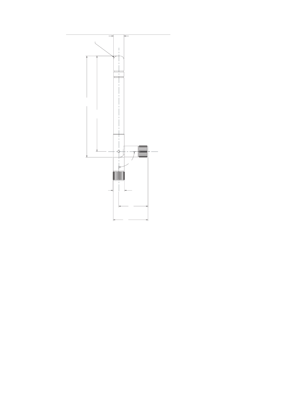
. . . . .
MODULE SPECIFICATIONS
Antenna specifications — 2 dBi Dipole
www.digiembedded.com 79
Antenna strength
(radiation
pattern) diagram
This diagram shows the strength of the signal received by the whip antenna on both
a horizontal and vertical plane. The diagram shows the magnetic field when the
antenna is in a vertical position. The red solid line represents the horizontal plane
and the green dotted line represents the vertical plane. You can see in the
illustration that at 90 degrees, the signal strength is 0 (as expected).
bOBITRON
SCALE 3.000
UNITS: mm
90.0˚
(9.1)
.360
(88.9)
3.500
(30.5)
1.200
(25.4)
1.010
(83.8)
3.300
(10.1)
.399
R
(3.2)
.125
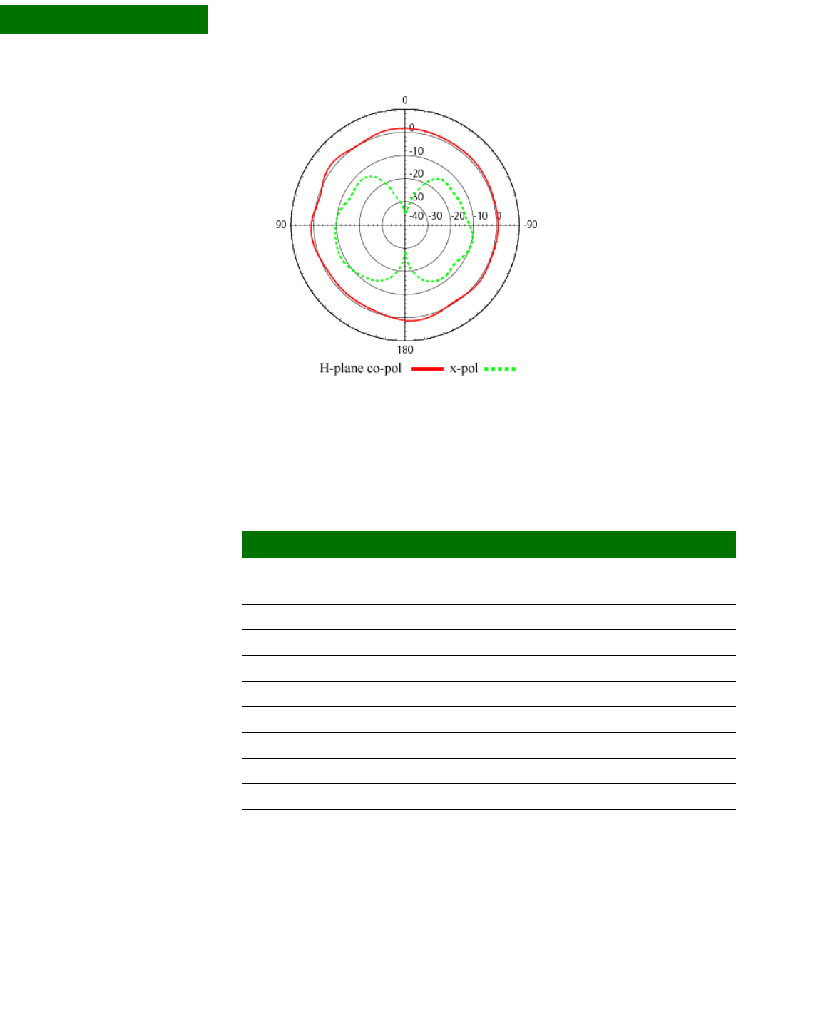
MODULE SPECIFICATIONS
Antenna specifications — 5 dBi Dipole
80 ConnectCore 9C/Wi-9C Hardware Reference, Rev. B 01/2007
A
. . . . . . . . . . . . . . . . . . . . . . . . . . . . . . . . . . . . . . . . . . . . . . . . . . . . . . . . . . . . . . . . . . . . . . . . . . . . . . . . . .
Antenna specifications — 5 dBi Dipole
Attributes
Dimensions (in
mm)
Note:
Dimensions are provided for reference purposes only. The actual antenna
might vary.
Antenna Attribute Band 1 Band 2
Frequency 2.4 ~ 2.5GHz 5.15~5.35 GHz
5.725~5.85 GHz
Power output 1W
DB gain 5 dBi (typ)
VSWR 2.0 max
Dimension See the measurements in the drawing after the table
Weight
Connector RP-SMA
Temperature rating -50 – +80C
Part number DG-ANT-55DP-AG
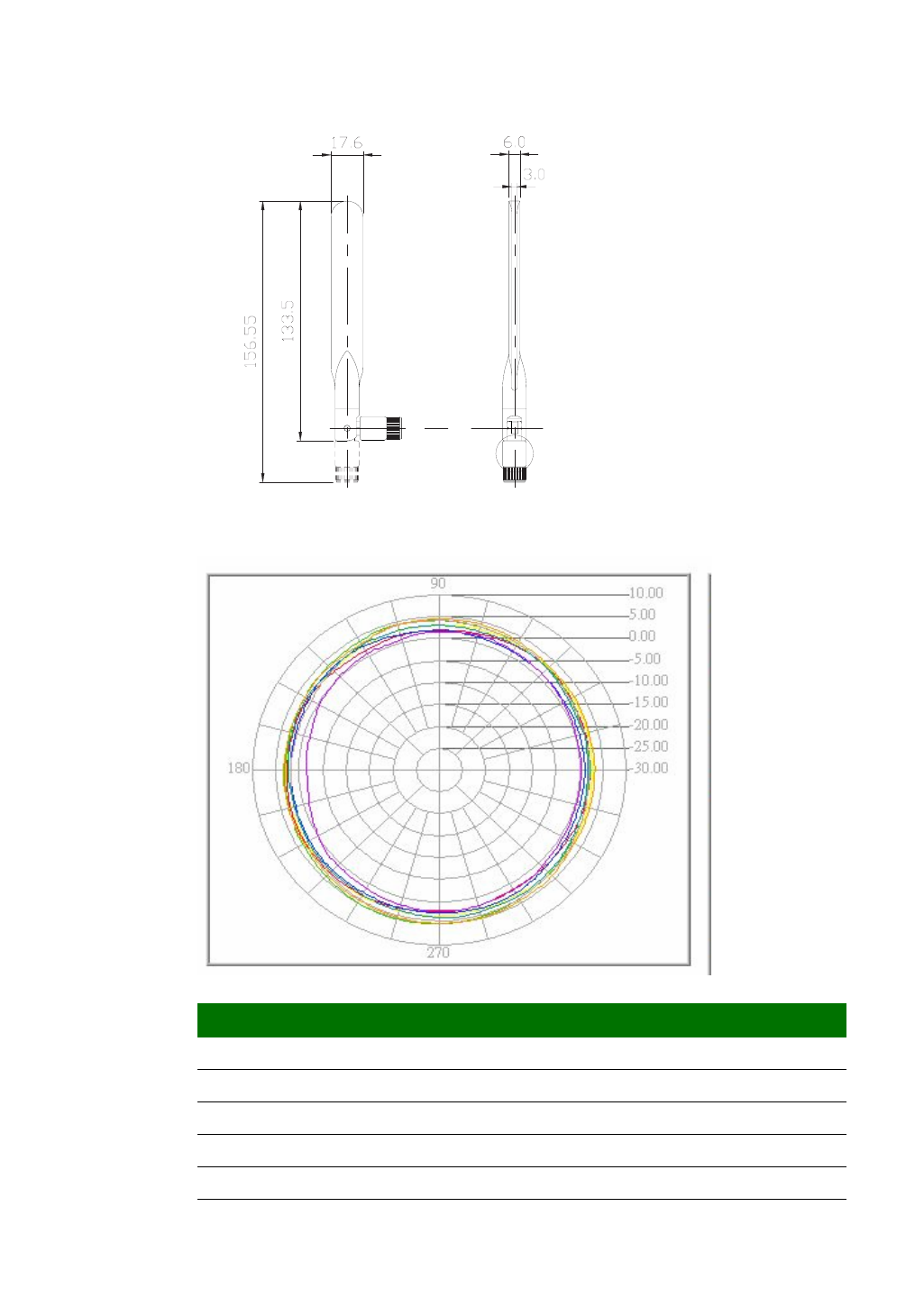
. . . . .
MODULE SPECIFICATIONS
Antenna specifications — 5 dBi Dipole
www.digiembedded.com 81
Radiation
pattern: H-Plane
(2.0 and 5.0 GHz)
Color Freq (MHz) Peak (dBi) Angle (o) Avg (dBi)
Yellow 2400.0 3.39 257.68 2.98
Red 2450.00 3.17 214.74 2.37
Blue 2500.00 2.79 288.0 1.96
Purple 5150.00 2.25 280.42 0.82
Green 5200.00 5.23 252.63 2.71
Light brown 5250.00 4.51 272.84 3.16
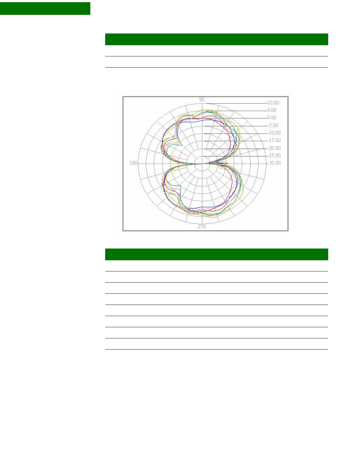
MODULE SPECIFICATIONS
Antenna specifications — 2 dBi PCB mount
82 ConnectCore 9C/Wi-9C Hardware Reference, Rev. B 01/2007
A
Radiation
pattern: E-plane
(2.0 and 5.0 GHz)
. . . . . . . . . . . . . . . . . . . . . . . . . . . . . . . . . . . . . . . . . . . . . . . . . . . . . . . . . . . . . . . . . . . . . . . . . . . . . . . . . .
Antenna specifications — 2 dBi PCB mount
The 2dBi PCB antenna is a surface-mount dual-band antenna.
Orange 5750.00 5.03 267.79 3.88
Aqua 5850.00 3.83 276.63 2.74
Color Freq (MHz) Peak (dBi) Angle (o) Avg (dBi)
Color Freq (MHz) Peak (dBi) Angle (o) Avg (dBi)
Yellow 2400.0 2.60 283.22 -1.10
Red 2450.00 2.57 240.42 -1.36
Blue 2500.00 1.92 237.27 -1.78
Purple 5150.00 2.37 78.67 -1.91
Green 5200.00 4.80 79.30 0.32
Light brown 5250.00 4.49 79.93 -0.01
Orange 5750.00 6.34 283.85 1.08
Aqua 5850.00 4.67 283.22 -0.46
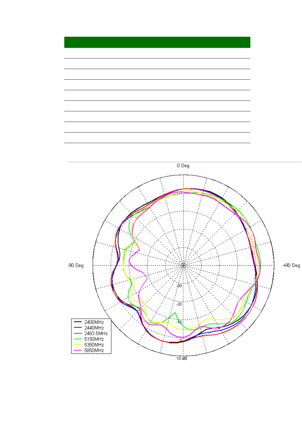
. . . . .
MODULE SPECIFICATIONS
Antenna specifications — 2 dBi PCB mount
www.digiembedded.com 83
Attributes
Radiation
patterns
Antenna Attribute Band 1 Band 2
Frequency 2.4 ~ 2.5GHz 4.9 ~ 5.9GHz
Power output 10W
DB gain >2 dBi
VSWR <2.5
Dimension 24.13 x 10.67 mm
Weight <1g
Connector U.FL
Temperature rating -40 – +85C
Part number DG-ANT-20CG-AG

MODULE SPECIFICATIONS
FCC RF radiation exposure statement
84 ConnectCore 9C/Wi-9C Hardware Reference, Rev. B 01/2007
A
. . . . . . . . . . . . . . . . . . . . . . . . . . . . . . . . . . . . . . . . . . . . . . . . . . . . . . . . . . . . . . . . . . . . . . . . . . . . . . . . . .
FCC RF radiation exposure statement
This equipment complies with FCC radiation exposure limits set forth for an
uncontrolled environment. The antenna(s) used for this transmitter must be
installed to provide a separation distance of at least 20 cm from all persons and
must not be co-located or operating in conjunction with any other antenna or
transmitter. End users must follow the specific operating instructions for satisfying
RF exposure compliance. This transmitter must not be co-located or operating in
conjunction with any other antenna or transmitter.
. . . . . . . . . . . . . . . . . . . . . . . . . . . . . . . . . . . . . . . . . . . . . . . . . . . . . . . . . . . . . . . . . . . . . . . . . . . . . . . . . .
Safety statements
To avoid contact with electrical current:
Never install electrical wiring during an electrical storm.
Never install an Ethernet connection in wet locations unless that connector is
specifically designed for wet locations.
Use caution when installing or modifying Ethernet lines.
Use a screwdriver and other tools with insulated handles.
You and those around you should wear safety glasses or goggles.
Do not place Ethernet wiring or connections in any conduit, outlet or junction
box containing electrical wiring.
Installation of inside wiring may bring you close to electrical wire, conduit,
terminals and other electrical facilities. Extreme caution must be used to avoid
electrical shock from such facilities. You must avoid contact with all such
facilities.
Color Frequency Mean gain Peak gain
Black 2400 0.70 3.49
Blue 2440 0.73 3.99
Red 2484 1.04 4.76
Green 5150 -1.51 3.03
Yellow 5350 -2.29 2.47
Pink 5850 -2.23 2.51
n/a Average -0.85 2.02

. . . . .
MODULE SPECIFICATIONS
Safety statements
www.digiembedded.com 85
Ethernet wiring must be at least 6 feet from bare power wiring or lightning
rods and associated wires, and at least 6 inches from other wire (antenna
wires, doorbell wires, wires from transformers to neon signs), steam or hot
water pipes, and heating ducts.
Do not place an Ethernet connection where it would allow a person to use an
Ethernet device while in a bathtub, shower, swimming pool, or similar
hazardous location.
Protectors and grounding wire placed by the service provider must not be
connected to, removed, or modified by the customer.
Do not touch uninsulated Ethernet wiring if lightning is likely!
Do not touch or move the antenna(s) while the unit is transmitting or receiving.
Do not hold any component containing a radio such that the antenna is very
close to or touching any exposed parts of the body, especially the face or eyes,
while transmitting.
Do not operate a portable transmitter near unshielded blasting caps or in an
explosive environment unless it is a type especially qualified for such use.
Any external communications wiring you may install needs to be constructed to all
relevant electrical codes. In the United States this is the National Electrical Code
Article 800. Contact a licensed electrician for details.


87
Dimensions and PCB Layouts
APPENDIX B
This appendix shows the dimensions of each module, as well as PCB (printed
circuit board) layouts of each.
Module
dimensions The next figures show the dimensions of the ConnectCore 9C/Wi-9C module.
Dimensions are in inches and millimeters (millimeter size is in brackets [ ]).
These are the tolerances for the drawings shown in this section:
Measure Tolerance
.XX ± .02
.XXX ± .010
Angles ± 2 degrees
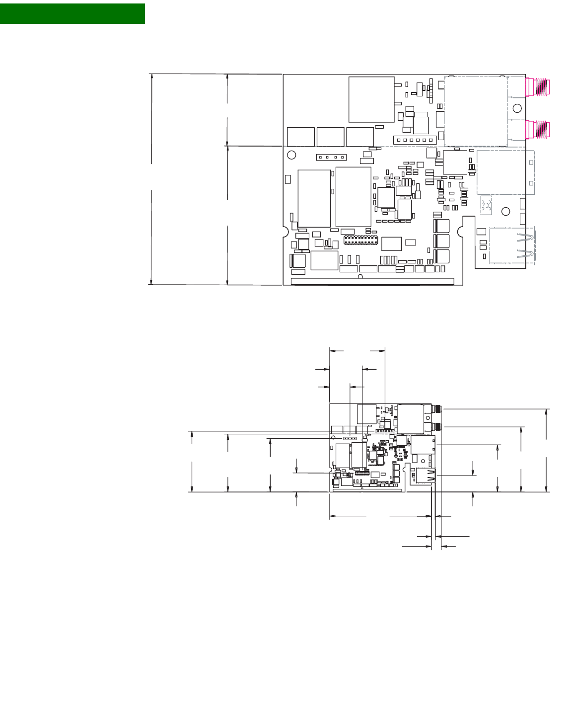
DIMENSIONS AND PCB LAYOUTS
88 ConnectCore 9C/Wi-9C Hardware Reference, Rev. B 01/2007
B
Overall view
Detailed views:
Top
#/..%#4#/2%#
"/!2$"/5.$!29
;=
;=
#/..%#4#/2% 7i-9C
"/!2$"/5.$!29
;=
3#!,%
;=
;=
;=
;=
;=
;=
;=
;=
; =
;=
;=
;=
;=
;=
#/..%#4#/2%#
"/!2$"/5.$!29
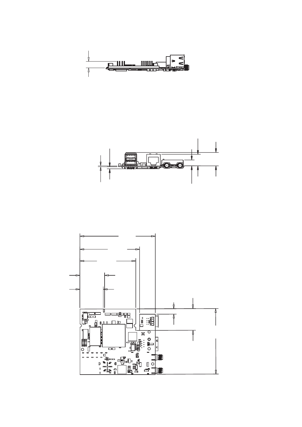
. . . . .
DIMENSIONS AND PCB LAYOUTS
www.digiembedded.com 89
Detailed views:
Side
Detailed views:
End
Detailed views:
Bottom
; =
;=
;=
;=
; =
;=
;
;
=
=
;
;
=
=
;
;
=
=
;
;
=
=
;
;
=
=
;
;
=
=
;
;
=
=
;
;
=
=
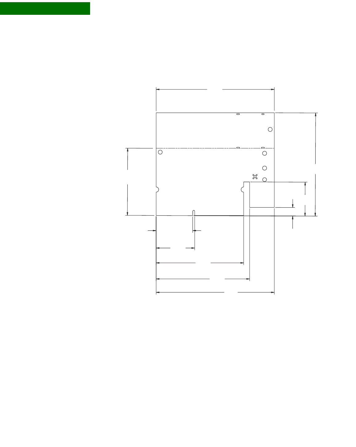
DIMENSIONS AND PCB LAYOUTS
PCB layout
90 ConnectCore 9C/Wi-9C Hardware Reference, Rev. B 01/2007
B
. . . . . . . . . . . . . . . . . . . . . . . . . . . . . . . . . . . . . . . . . . . . . . . . . . . . . . . . . . . . . . . . . . . . . . . . . . . . . . . . . .
PCB layout
The next figures show the PCB layout of the ConnectCore 9C/Wi-9C module.
Overall view
View with detail This figure shows the view with detail for the areas marked Detail A and Detail B.
;=
;=
;=
;=
;=
;=
;=
;=
;=
#/..%#4#/2%#
"/!2$"/5.$!29
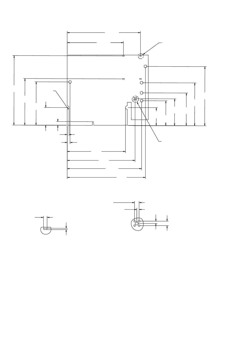
. . . . .
DIMENSIONS AND PCB LAYOUTS
PCB layout
www.digiembedded.com 91
3#!,%
3%%$%4!),!
3%%$%4!),"
$%4!),!
; =
;=
8
;=
;=
;=
;=
;=
;=
;=
;=
;=
;=
;=
;=
;=
8
;=
8
;=
8
;=
8
;=
;=
;=
2
;=
$%4!),"
;=
;=
;=
;=


93
Certifications
APPENDIX C
The ConnectCore 9C and ConnectCore Wi-9C products comply with the standards
cited in this section.
. . . . . . . . . . . . . . . . . . . . . . . . . . . . . . . . . . . . . . . . . . . . . . . . . . . . . . . . . . . . . . . . . . . . . . . . . . . . . . . . . .
FCC Part 15 Class B
Radio Frequency Interface (RFI) (FCC 15.105)
The ConnectCore 9C and ConnectCore Wi-9C embedded modules have been tested
and found to comply with the limits for Class B digital devices pursuant to Part 15
Subpart B, of the FCC rules. These limits are designed to provide reasonable
protection against harmful interference in a residential environment. This
equipment generates, uses, and can radiate radio frequency energy, and if not
installed and used in accordance with the instruction manual, may cause harmful
interference to radio communications. However, there is no guarantee that
interference will not occur in a particular installation. If this equipment does cause
harmful interference to radio or television reception, which can be determined by
turning the equipment off and on, the user is encouraged to try and correct the
interference by one or more of the following measures:
Reorient or relocate the receiving antenna.
Increase the separation between the equipment and receiver.
Connect the equipment into an outlet on a circuit different from that to which
the receiver is connected.
Consult the dealer or an experienced radio/TV technician for help.

CERTIFICATIONS
FCC Part 15 Class B
94 ConnectCore 9C/Wi-9C Hardware Reference, Rev. B 01/2007
C
Labeling Requirements (FCC 15.19)
This device complies with Part 15 of FCC rules. Operation is subject to the following
two conditions: (1) this device may not cause harmful interference, and (2) this
device must accept any interference received, including interference that may
cause undesired operation.
If the FCC ID is not visible when installed inside another device, then the outside of
the device into which the module is installed must also display a label referring to
the enclosed module FCC ID. THis exterior label can use wording such as the
following: “Contains Transmitter Module FCC ID: MCQ-50M1355/ IC: 1846A-
50M1355”.
Modifications (FCC 15.21)
Changes or modifications to this equipment not expressly approved by Digi may void
the user’s authority to operate this equipment.
Industry Canada
This digital apparatus does not exceed the Class B limits for radio noise emissions
from digital apparatus set out in the Radio Interference Regulations of the Canadian
Department of Communications.
Le present appareil numerique n’emet pas de bruits radioelectriques depassant les
limites applicables aux appareils numeriques de la class B prescrites dans le
Reglement sur le brouillage radioelectrique edicte par le ministere des
Communications du Canada.

. . . . .
CERTIFICATIONS
FCC Part 15 Class B
www.digiembedded.com 95
Declaration of Conformity
(In accordance with FCC Dockets 96-208 and 95-19)
Digi International declares, that the product:
to which this declaration relates, meets the requirements specified by the Federal
Communications Commission as detailed in the following specifications:
Part 15, Subpart B, for Class B equipment
FCC Docket 96-208 as it applies to Class B personal
Personal computers and peripherals
The product listed above has been tested at an External Test Laboratory certified
per FCC rules and has been found to meet the FCC, Part 15, Class B, Emission
Limits. Documentation is on file and available from the Digi International
Homologation Department.
Manufacturer’s Name: Digi International
Corporate Headquarters: 11001 Bren Road East
Minnetonka MN 55343
Manufacturing Headquarters: 10000 West 76th Street
Eden Prairie MN 55344
Product Name: ConnectCore 9C
Model Numbers: 50001327-xx
Product Name ConnectCore Wi-9C
Model Numbers: 50001355-xx

CERTIFICATIONS
FCC Part 15 Class B
96 ConnectCore 9C/Wi-9C Hardware Reference, Rev. B 01/2007
C
International EMC Standards
The ConnectCore 9C and ConnectCore Wi-9C meet the following standards:
Standards ConnectCore 9C ConnectCore Wi-9C
Emissions AS/NZS 3548 AS/NZS 3548 CISPR 22
FCC Part 15 Subpart C
(FCC ID: MCQ-50M1355)
IC RSS 210 (IC:1846A-50M1355)
FCC Part 15 Subpart B
ICES-003
EN 55022
EN 61000-4-2
EN 61000-4-3
EN 61000-4-6
EN 301 489-3
EN 300 328
VCC1
EN 55024
UL 60950-1
CSA C22.2, No. 60950-1
EN60950
Immunity
Safety

Index-1
Index
. . . . . . . . . . . . . . . . . . . . . . . . . . . . . . . . . . . . . . . . . . . . . . . . . . . . . . . . . . . . . . . . . . . . . . . . . . . . . . .
Numerics
802.3af Power over Ethernet (PoE) connector,
P20. See Power over Ethernet (PoE)
connector, P20 (dev board)
802.3af Power over Ethernet (PoE) pass-through
connector, P5. See Power over Ethernet
(PoE) pass-through connector, P5
(module).
9-30VDC power input 30
A
absolute maximum ratings 75
antenna connectors 26
-
27
antenna information 77
-
84
antenna specifications
2 dBi Dipole 78
2 dBi PCB mount 82
5 dBi Dipole 80
application-specific expansion connectors 29,
43
B
board and module mounting holes 30
buttons and switches 31
C
certifications 93
CMO. See current measurement option.
colors and gray shades (LCD) 60
configurations
ConnectCore 9C 5
ConnectCore Wi-9C 7
ConnectCore 9C
about 1
-
9
configurations 5
environmental information 66
features 1
mechanical dimensions 65
power requirements 67
ConnectCore Wi-9C
about 1
-
9
antenna connectors 26
-
27
configurations 7
environmental information 66
features 1
mechanical dimensions 65
power requirements 67
RP-SMA connectors 27
security standards 2
U.FL connectors 27
WLAN 3
WLAN interface 2
ConnectCore Wi-9C antenna options 2
control and data pins (LCD) 59
CR1 14
CR2 14
CR3 and CR5, power LEDs 54
CR6 and CR7, user LEDs 54
current measurement option (CMO) 30, 55
D
daughter cards 43
DC electrical characteristics 76
development board 29
-
58
9-30VDC power input 30
application-specific expansion
connectors 29
board and module mounting holes 30

Index-2ConnectCore 9C/Wi-9C Hardware Reference, Rev B 01/2007
Index
current measurement option 30, 55
description 30
digital I/O connector, P19 49
digital I/Os VGA interface 29
external LCD clock, G1 40
features 29
hardware reset switch, SW6 32
I2C header connector, P8 33
I2C interface 29
LCD connectors 29
LEDs 29, 54
-
55
P16, peripheral board header 43, 44
P17, platform application header 43, 45
P18, LCD application header 46
P30, PoE connector 51
P31, PoE connector 51
P32, USB Device application header 48
power jack, P12 57
power on/off switch 30
Power over Ethernet(PoE) connector,
P20 51
power switch, SW5 32
pushbuttons, SW3 and SW4 29, 32
serial port A connector, P13 35
serial port B connector, P9 36
serial port C connector, P10 37
serial port connectors 35
-
38
serial port D connector, P11 37
serial ports 29
SO-DIMM connector, P15 40
-
42
SPI header connector, P7 34
SPI interface 29
SW1, Serial Port A switch 31
SW2, Serial Port B switch 32
SW7, VGA (enable) switch 32
test points 29, 57
through-hole prototyping (wrap-field) area,
P3 and P4 52
VGA connector, P6 39
VGA interface 29
digital I/O connector, P19 49
E
edge connector, P3 18
electrical characteristics 75
environmental information
ConnectCore 9C module 66
ConnectCore Wi-9C 66
Ethernet connector 12
-
13
connector pins 12
LEDs 12
Ethernet interface 2
Ethernet with LEDs 12
external LCD clock, G1 40
external memory bus 4
F
factory default interface configuration 58
G
G1, external LCD clock 40
H
hardware reset switch, SW6 32
I
I2C header connector 33
I2C interface 4, 29
I2C signals 67
interfaces
Ethernet 2
external memory bus 4
I2C 4, 29
LCD controller 4
serial port 4, 35
-
38
SPI 29
USB Host/Device 3
VGA 29
WLAN 3
J
JTAG 20-pin header connector, P2 15

. . . . .
www.digiembedded.com Index-3
JTAG adapter 16
assembly 17
L
LCD application header, P18 46
LCD connectors 29
LCD controller
interface 4
number of colors 60
LCD displays 59
-
62
LCD refresh frequency 61
LCD resolution 61
LEDs 12
development board 54
-
55
power 54
serial 54
user 54
LEDs (user) 29
M
mechanical dimensions
ConnectCore 9C module 65
ConnectCore Wi-9C 65
memory 2
memory clocks 2
module 13
antenna connectors 26
-
27
edge connector, P3 18
Ethernet connector 12
-
13
JTAG header connector, P2 15
LEDs, CR1 and CR2 14
USB Host connector, P6 18
module dimensions 87
-
89
module layout 11
module LEDs, CR1 and CR2 14
module reset 69
module specifications 65
-
85
N
network interface
Ethernet 66
WLAN 66
P
P10, serial port C connector 37
P11, serial port D connector 37
P12, power jack 57
P13, serial port A connector 35
P15, SO-DIMM connector (development
board) 40
-
42
P16, peripheral board header 43, 44
P17, platform application header 43, 45
P18, LCD application header 46
P19, digital I/O connector 49
P2, JTAG 20-pin header connector 15
P20, Power over Ethernet (PoE) connector (dev
board) 51
P3 and P4, through-hole prototyping (wrap-
field) area (dev board) 52
P3, edge connector (module) 18
P30, PoE connector 51
P31, PoE connector 51
P32, USB Device application header 48
P5, Power over Ethernet (PoE) pass-through
connector (module) 13
P6, USB Host connector (module) 18
P6, VGA connector (dev board) 39
P7, SPI header connector 34
P8, I2C header connector 33
P9, serial port B connector 36
PCB layouts 90
-
91
peripheral board header, P16 43, 44
platform application header, P17 43, 45
PoE connector, P30 51
PoE connector, P31 51
PoE support 13
power dissipation 76
power jack, P12 57
power LEDs 54
power on/off switch 30
Power over Ethernet (PoE) connector, P20 51
Power over Ethernet (PoE) pass-through
connector, P5 13
Power over Ethernett (PoE) connectors 50
power requirements

Index-4ConnectCore 9C/Wi-9C Hardware Reference, Rev B 01/2007
Index
ConnectCore 9C 67
ConnectCore Wi-9C 67
power switch, SW5 32
power up 67
pushbuttons (user) 29
R
real-time clock 67
recommended operating conditions 75
RF exposure statement 84
RP-SMA connectors 27
primary, P10 27
secondary, P8 27
S
safety statements 84
sample applications (LCD) 61
serial LEDs 54
serial port A (EIA-232/422/485) interface 35
serial port A connector 35
Serial Port A switch, SW1 31
serial port B (EIA-232) interface 36
serial port B connector 36
Serial Port B switch, SW2 32
serial port C connector 37
serial port C interface 37
serial port connectors 35
-
38
serial port D connector 37
serial port D interface 37
serial port interface 4
serial ports 29
SO-DIMM connector, P15 40
-
42
inserting 41
pin assignment 42
pin orientation 43
SPI header connector 34
SPI interface 29
SW1, Serial Port A switch 31
SW2, Serial Port B switch 32
SW3, USER_PUSH_BUTTON_1 32
SW4, USER_PUSH_BUTTON_2 32
SW5, power switch 32
SW6, hardware reset switch 32
SW7, VGA (enable) switch 32
switches
SW1, Serial Port A 31
SW2, Serial Port B 32
SW3 and SW4, user-programmable
pushbuttons 32
SW5, power 32
SW6, hardware reset 32
SW7, VGA (enable) 32
switches and buttons 31
system clocks 2
T
test points 29, 57
through-hole prototyping (wrap-field) area, P3
and P4 52
through-hole signal rail, P3 52
U
U.FL connectors 27
primary, P11 27
secondary, P9 27
USB configuration 63
USB Device application header, P32 48
USB Host and Device interface 3
USB Host connector, P6 (module) 18
USB interface 68
-
69
no USB on module 68
USB Device only 69
USB Host with hub on module 68
USB Host/Device 68
USB internal PHY DC electrical
characteristics 77
user LEDs 54
user pushbuttons 32
V
VGA (enable) switch, SW7 32
VGA connector, P6 (dev board) 39
VGA interface 29

