Digi 50M1538 WLAN Module User Manual
Digi International Inc WLAN Module
UserManual.wiki
>
Digi
>
50M1538 User Manual
User manual
Navigation menu
Upload a User Manual
Namespaces
Wiki Guide
HTML
PDF
Info
Views
User Manual
Discussion / Help
Navigation
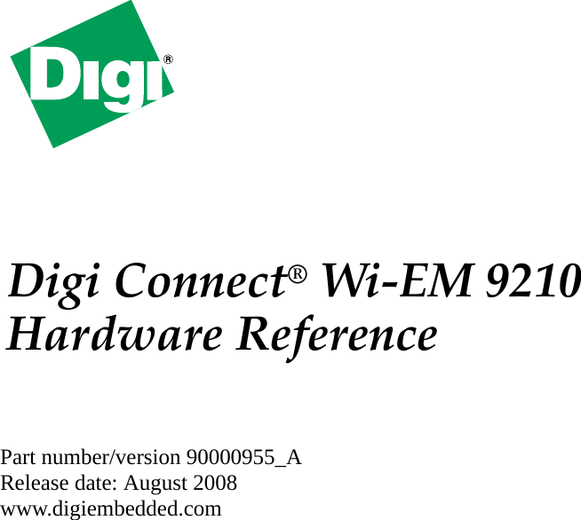
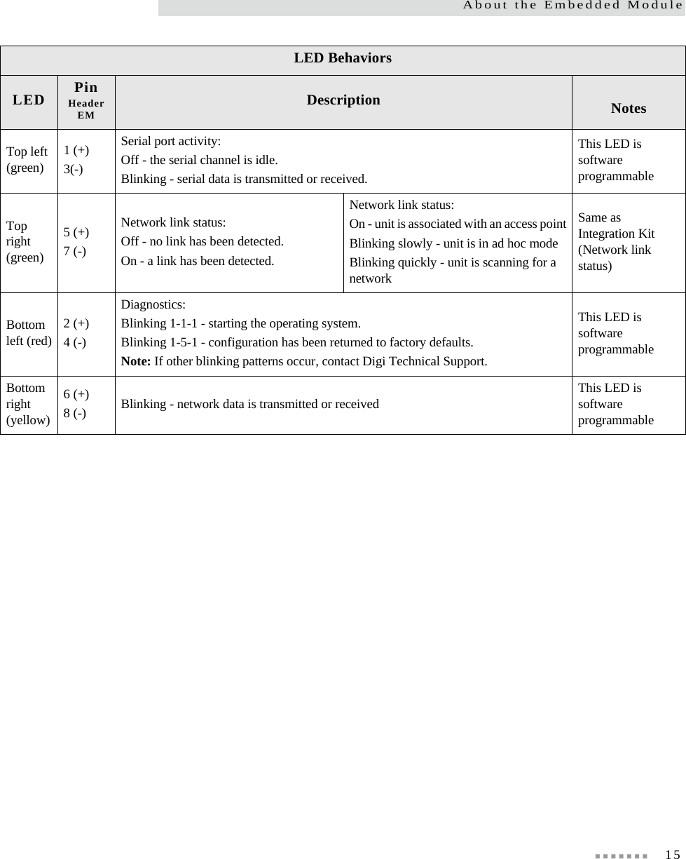
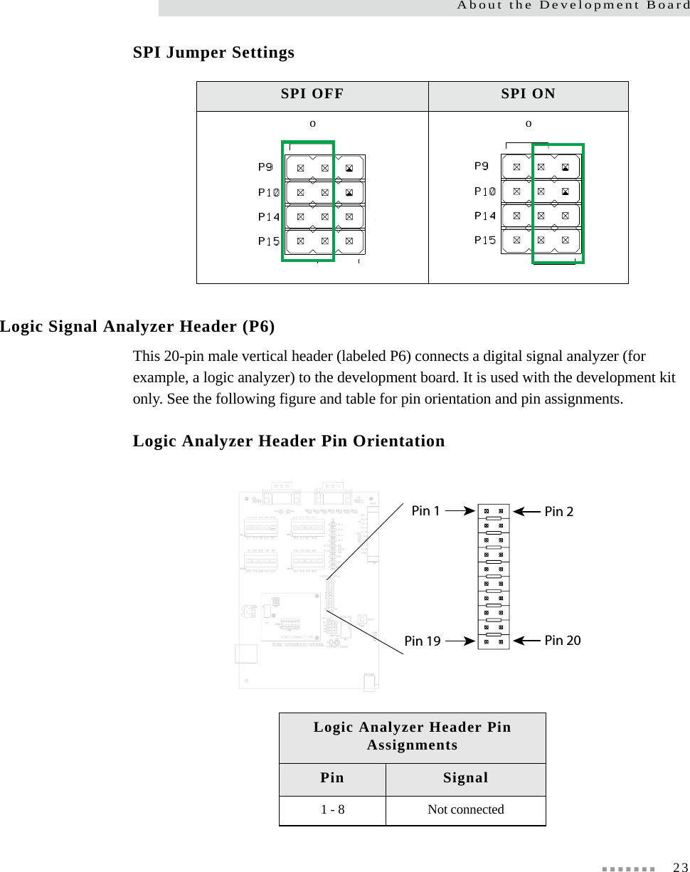
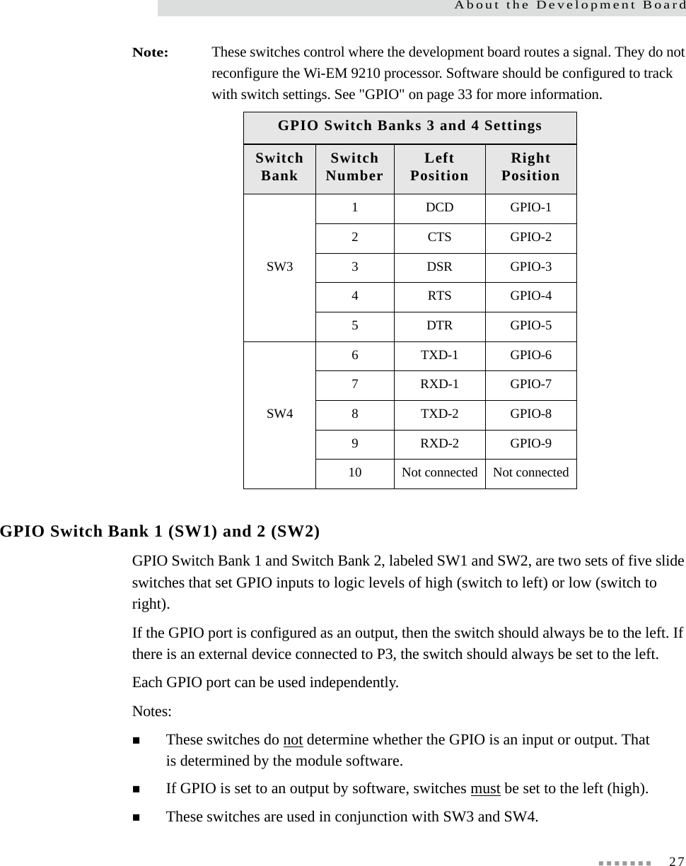

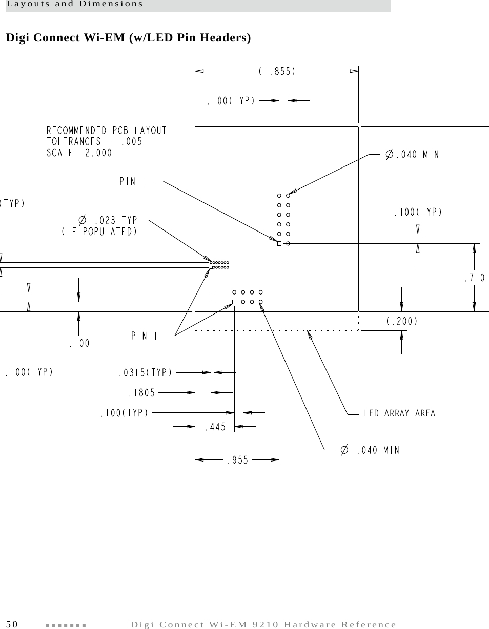
![GPIO34 Digi Connect Wi-EM 9210 Hardware ReferenceGPIO RegistersSix registers govern the 16 GPIO pins. There are four configuration registers. Each has eight bits dedicated to the configuration of each GPIO.. Each GPIO configuration section is set up the same way. The following table shows the settings using bits D07:00; the same settings apply to the corresponding bits in D31:24, D23:D16, and D15:08.GPIO pin configuration registersRegister D31:24 D23:D16D15:08 D07:00A090 2000, config 0 GPIO [15] GPIO [14] GPIO [13] GPIO [12]A090 2004, config 1 GPIO [11] GPIO [10] GPIO [9] GPIO [8]A090 2008, config 2 GPIO [7] GPIO [6] GPIO [5] GPIO [4]A090 200C, config 3 GPIO [3] GPIO [2] GPIO [1] GPIO [0]GPIO ConfigurationSetings using bits D07:00D07:06 Reserved N/AD05:03 FUNCUse these bits to select the function you want to use. For a detailed description of each function see the NS 9210 HRM in the Pinout chapter under "General purpose I/O (GPIO)" and the "GPIO pin use" table in this manual.000 Function #0001 Function #1010 Function #2RESET_DONE - default for GPIO[12]011 Function #3GPIO - default, except for GPIO[12]100 Function #4](https://usermanual.wiki/Digi/50M1538/User-Guide-1009467-Page-34.png)
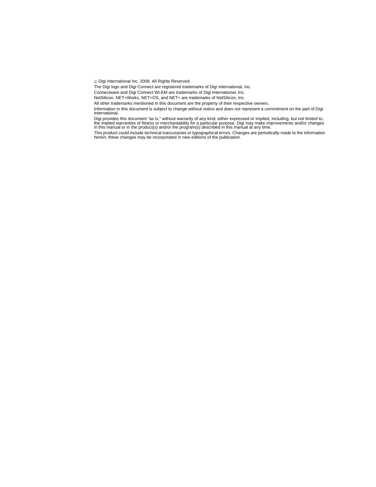
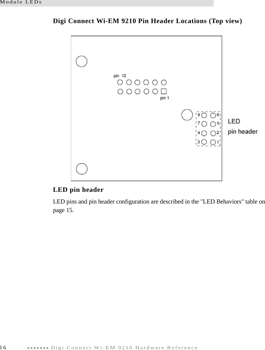
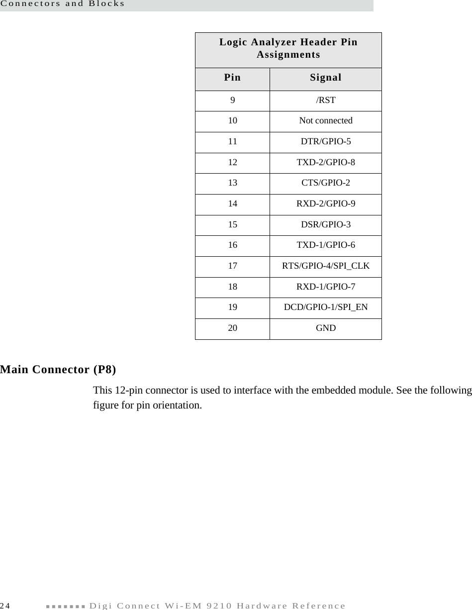
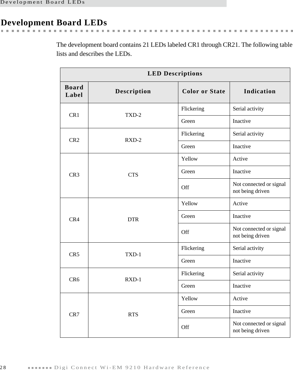
![ 35Programming ConsiderationsD02 DIRControls the pin direction when the FUNC field is configured for GPIO mode, function #3.0 Input1 OutputAll GPIO pins reset to the input state.Note: The pin direction is controlled by the selected function in modes #0 through #2.D01 INVControls the inversion function of the GPIO pin.0 Disables the inversion function1 Enables the inversion functionThis bit applies to all functional modes.D00 PUDIS Controls the GPIO pin pullup resistor operation.0 Enables the pullup1 Disables the pullupNote: The pullup cannot be disabled on GPIO[9], GPIO[12]GPIO ConfigurationSetings using bits D07:00](https://usermanual.wiki/Digi/50M1538/User-Guide-1009467-Page-35.png)
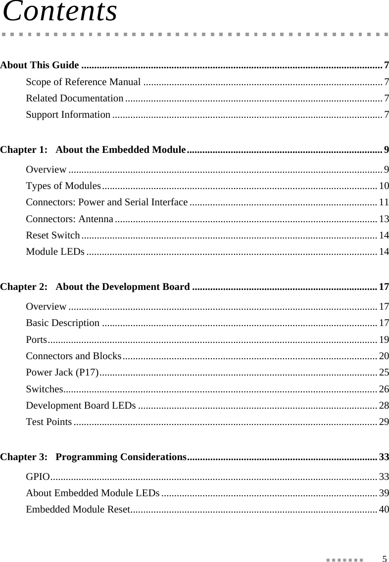
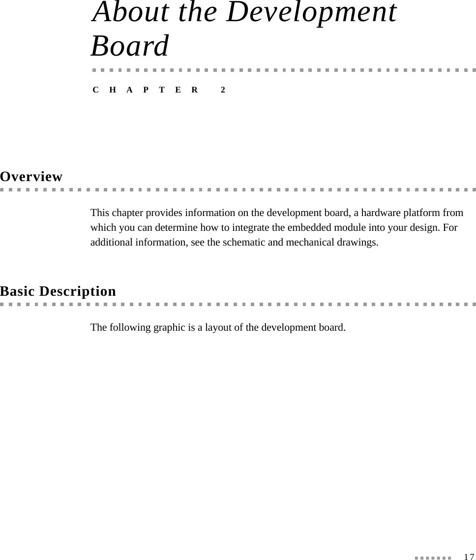
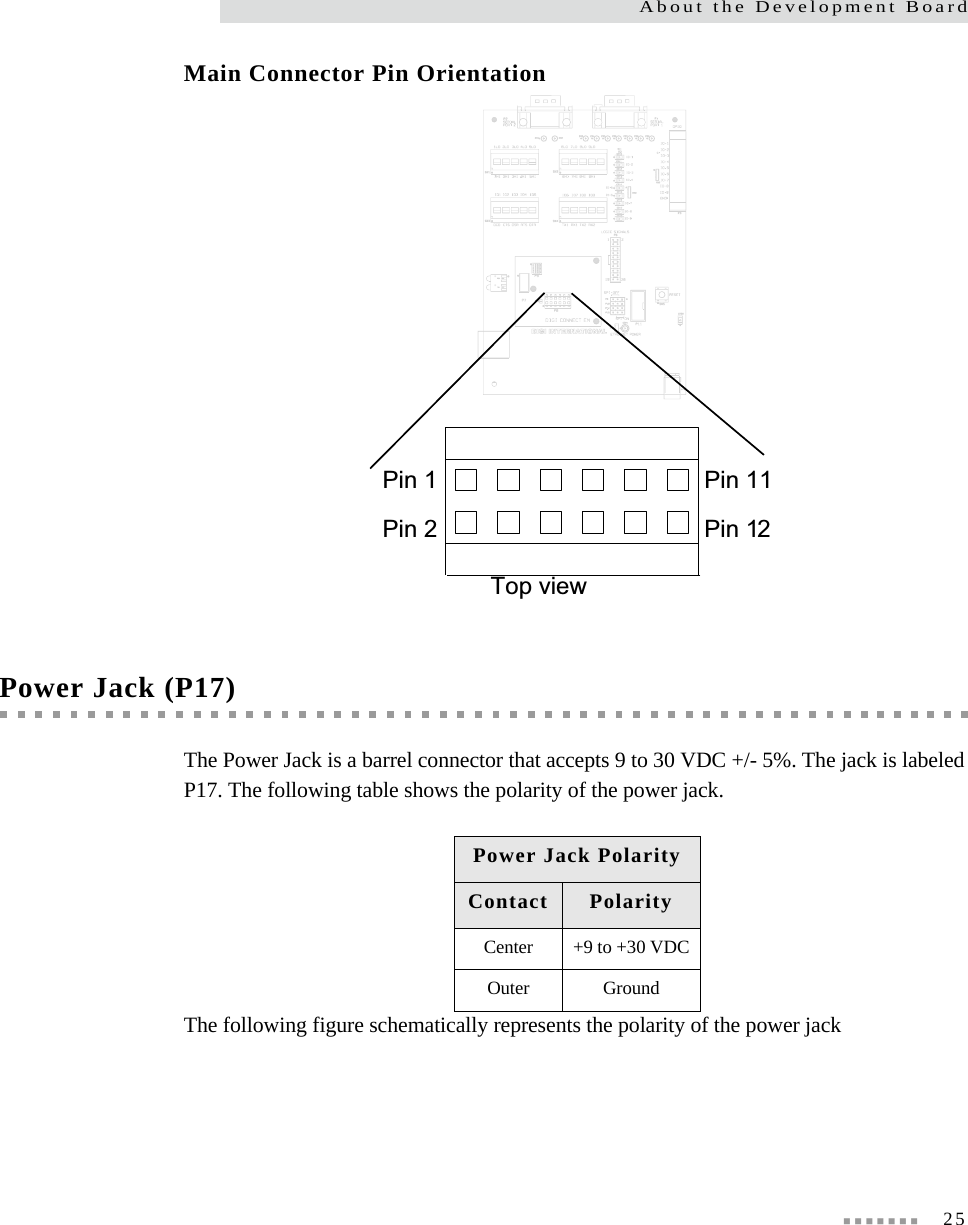
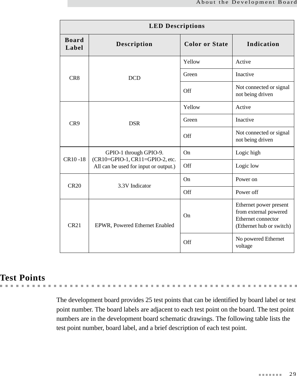
![GPIO36 Digi Connect Wi-EM 9210 Hardware ReferenceGPIO [15:0] Control Register There is one GPIO control Register that governs all 16 GPIO pins. When a GPIO pin is configured as a GPIO output, the corresponding bit in the GPIO Control Register is driven out the GPIO pin. In all configurations, the CPU has read/write access to these registers. Register bits D31:16 are unused GPIO pins. These pins are being used as memory data bits 15:00. It is safest to read all 32 bits, modify the bit(s) corresponding to the GPIO(s) of interest, and then write back the full 32 bits. In this way the behavior of the other GPIO lines will be preserved.GPIO [15:0] Status RegisterThere is one GPIO Status Register. This register contains the status information for each of the 16 GPIO pins. Bits D31:16 are used as memory data therefore their status will not be meaningful. In all configurations, the value on the GPIO input pin is brought to the status register and the CPU has read-only access to this register.Register D31:24 D23:D16 D15:08 D07:00A090 206C GPIO [31:24] not used] GPIO [23:16] not used GPIO [15:8] GPIO [7:0]Register D31:24 D23:D16 D15:08 D07:00A090 207C GPIO [31:24] not used] GPIO [23:16] not used GPIO [15:8] GPIO [7:0]](https://usermanual.wiki/Digi/50M1538/User-Guide-1009467-Page-36.png)
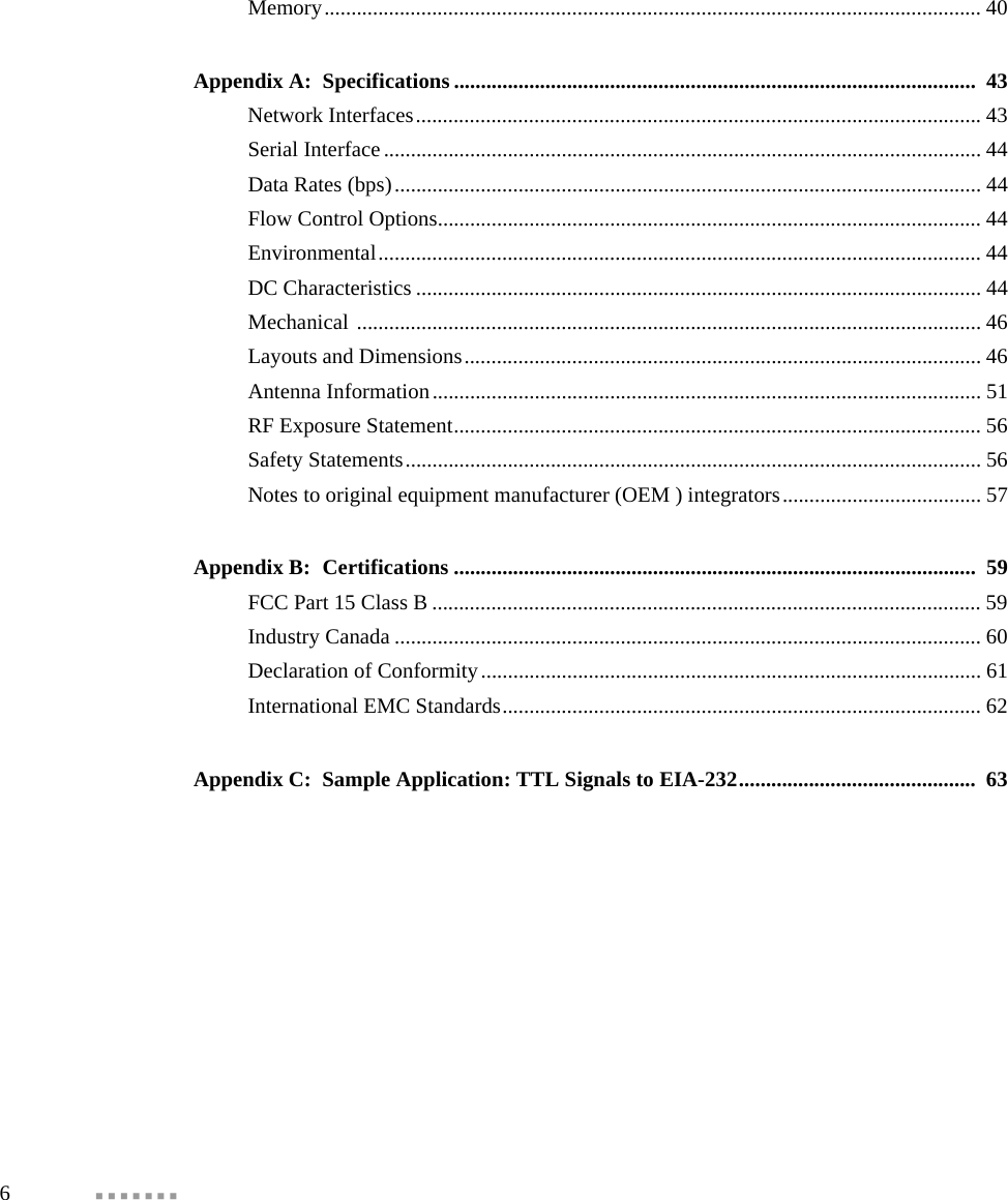
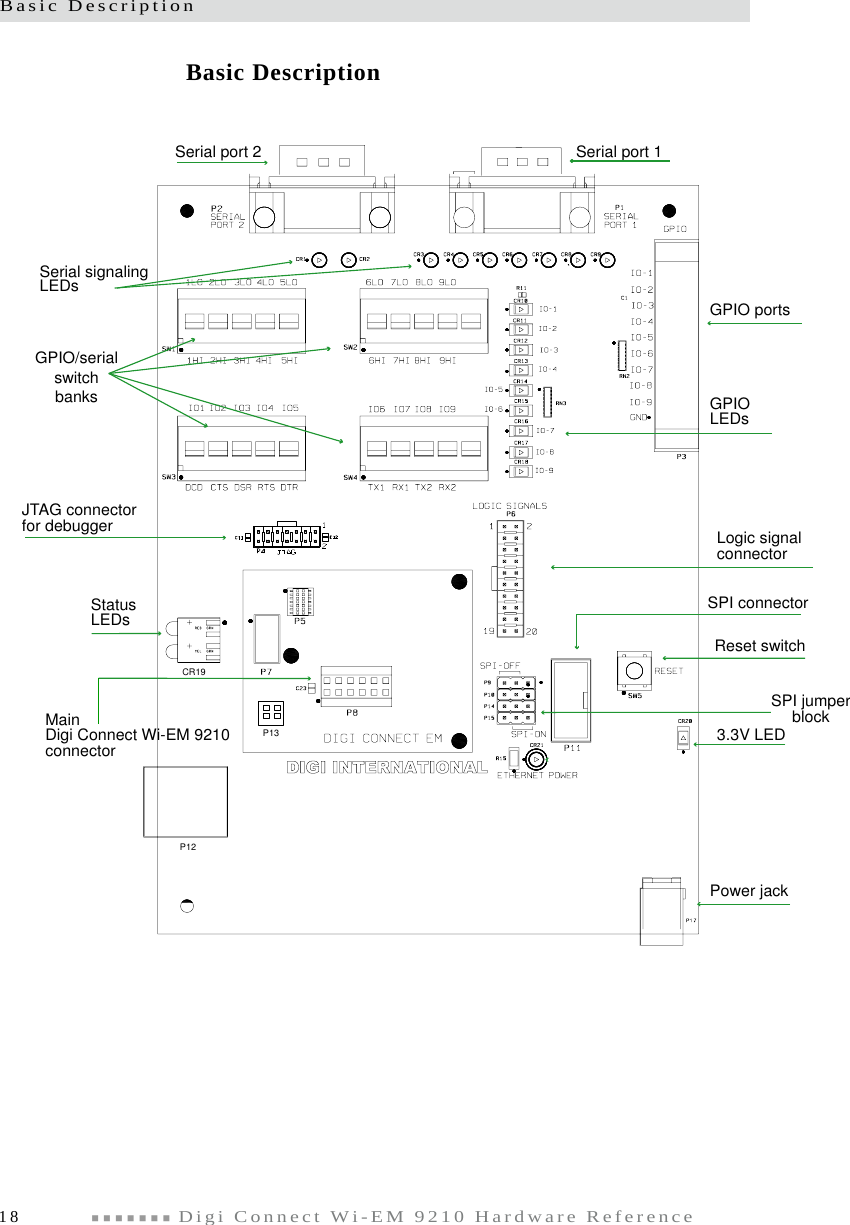
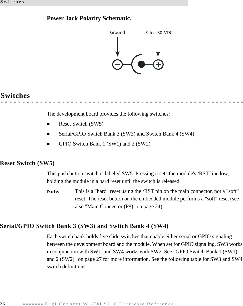
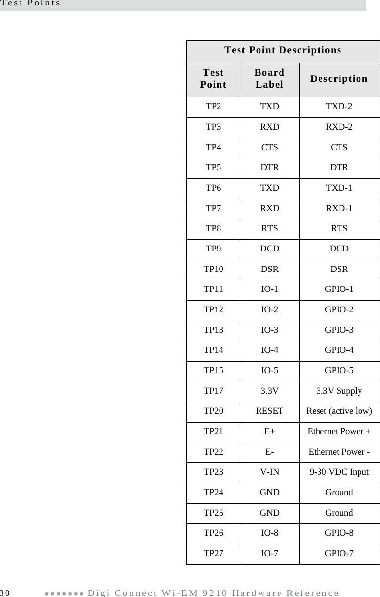
![ 37Programming ConsiderationsGPIO pin use tableGPIO Pin UseName RegisterBit Category ExternalInterface DescriptionTXSD/SPI_TX/GPIO-6 GPIO[7] Allocated Pin 4 on the main header Used for the serial TXD or SPI_TX, but could be reassigned as a GPIO, timer out 7 or in 8. If used with the development board, this pin maps to GPIO-6.DTR/GPIO-5GPIO[6] Allocated Pin 6 on the main header Usedc for the serial DTR but could be reassigned as a GPIO, or timer in 7. If used with the development board, this pin maps to GPIO-5.RTS/SPI_CLK/GPIO-4 (See description)GPIO[5]or GPIO[4] Allocated Pin 5 on the main headerSince these two processor pins map to the same header pin, one must be configured as an input to avoid contention.UART: GPIO[5] is confiured for RTS and GPIO[4] for GPIO input.SPI: GPIO[5] for GPIO input and GPIO[4] for SPI_CLK.Other: GPIO[5] supports IRQ3 and timer out 6.GPIO[4] supports IRQ2 and timer in 6. If used with the development board, header pin 5 maps to GPIO-4.RXD/SPI_RX/GPIO-7 GPIO[3] Allocated Pin 3 on the main headerUsed for the serial RXD or SPI_RX, but could be reassigned as a GPIO or PICO-3. If used with the development board, this pin maps to GPIO-7.DSR/GPIO-3GPIO[2] Allocated Pin 9 on the main headerUsed for the serial DSR, but could be reassigned as a GPIO or PICO-2. If used with the development board, this pin maps to GPIO-3.](https://usermanual.wiki/Digi/50M1538/User-Guide-1009467-Page-37.png)
![GPIO38 Digi Connect Wi-EM 9210 Hardware ReferenceCTS/GPIO-2GPIO[1] Allocated Pin 7 on the main headerUsed for the serial CTS, but could be reassigned as a GPIO, IRQ0 or PICO-1. If used with the development board, this pin maps to GPIO-2.DCD//SPI_EN/GPIO-1 GPIO[0] Allocated Pin 8 on the main headerUsed for the serial DCD or SPI_EN, but could be reassugned as a GPIO or PICO-0. If used with the development board, this pin maps to GPIO-1.TXD2/GPIO-8 GPIO[15] Allocated Pin 12 on the main headerUsed for the serial2 TXD, but could be reassigned as a GPIOor timer in 9. If used with the development board, this pin maps to GPIO-8.Network link Green LED GPIO[14] ReservedConnected to the Green LED above the Yellow LEDNetwork link status:On - unit is associated with an access point Blinking slowly - unit is in ad hoc modeBlinking quickly - unit is scanning for a network/INIT GPIO[13] Available Connected to the button on the module Should be configured as a GPIO input.Serial Port activity LED/MFGO GPIO [12] AllocatedConnected to the green LED above the red LEDUsed as the NET+OS green LED, but can be reassigned as a general purpose LED. It must remain a GPIO output for the LED to operate correctly. The LED is lit when the signal is low.RXD2/GPIO-9 GPIO[11] Allocated Pin 11 on the main headerUsed for the serial2 RXD, but could be reassigned as a GPIO or IRQ2. If used with the development board, this pin maps to GPIO-9.IRQ1 GPIO[10] Reserved N/A N/AGPIO Pin UseName RegisterBit Category ExternalInterface Description](https://usermanual.wiki/Digi/50M1538/User-Guide-1009467-Page-38.png)
![ 39Programming ConsiderationsNote: The Wi-EM 9210 signals PIC0-[0:3] provided by the programmable FIMs(DRPIC) are only applicable when running NET+OS.About Embedded Module LEDsMFGI GPIO[9] Reserved N/A N/ARed LED GPIO[8] Allocated Connected to the Red LED Used for diagnostics and power on indication.GPIO Pin UseName RegisterBit Category ExternalInterface DescriptionEmbedded Module LED DescriptionLED DescriptionGreen (above yellow LED) This LED is wired to the network hardware and provides an indication of link status.Green(the one above the red LED)This LED is software programmable and is wired to processor GPIO register bit GPIO[12] and wired to be lit when low. Use for serial port activity.Yellow This LED is wired to the network hardware and provides an indication of network activity.Red This LED is software programmable, wired to processor GPIO register bit GPIO[8], and wired to be lit when low. LED ON indicates power on and is in addition used for diagnostics.](https://usermanual.wiki/Digi/50M1538/User-Guide-1009467-Page-39.png)
![Embedded Module Reset40 Digi Connect Wi-EM 9210 Hardware ReferenceEmbedded Module Reset Hard ResetThe embedded modules support a hardware reset on pin 10 of the 12-pin header. The unit will be forced into a hard reset if this pin is pulled low. When used with the development board, this pin is wired to reset button SW5, which means it acts as a hard reset button.The JTAG version of the Wi-EM 9210 EM module has a 3-pin jumper (JP1) to allow two modes of operation.Shorted 1-2: The CPU and other registers are reset. The PLL, GPIOs, and memory are not. Debugger connection is maintained. This is the same as SRST# from the debugger.Shorted 2-3: The entire module is reset. Debugger connection will need to be re-established.Soft ResetNET+OS provides an internal facility to enact a soft reset, but it is the responsibility of a specific implementation to choose a reasonable trigger to invoke it. One choice is to use a GPIO pin as a signal to trigger a soft reset. The embedded modules have one GPIO pin GPIO[13] which is not normally assigned to any other task named "/INIT." It is an ideal candidate for use as a signal for soft reset. The signal is wired to the push button on the module (next to the LEDs), and is pulled high unless the button is pushed. The "naresetapp" sample application demonstrates a simple mechanism for monitoring a GPIO pin and then initiating a soft reset when the pin achieves a particular value.MemoryFlashThe Wi-EM 9210 module has 4 MB of flash memory, which is controlled by chip select 2 (default = st_cs1) located at 0x50000000.](https://usermanual.wiki/Digi/50M1538/User-Guide-1009467-Page-40.png)